JP2013507665A - 共同パッケージ化された半導体光学装置 - Google Patents
共同パッケージ化された半導体光学装置 Download PDFInfo
- Publication number
- JP2013507665A JP2013507665A JP2012533704A JP2012533704A JP2013507665A JP 2013507665 A JP2013507665 A JP 2013507665A JP 2012533704 A JP2012533704 A JP 2012533704A JP 2012533704 A JP2012533704 A JP 2012533704A JP 2013507665 A JP2013507665 A JP 2013507665A
- Authority
- JP
- Japan
- Prior art keywords
- optical
- ferrule
- semiconductor
- optical fibers
- semiconductor optical
- Prior art date
- Legal status (The legal status is an assumption and is not a legal conclusion. Google has not performed a legal analysis and makes no representation as to the accuracy of the status listed.)
- Pending
Links
- 230000003287 optical effect Effects 0.000 title claims abstract description 153
- 239000004065 semiconductor Substances 0.000 title claims abstract description 125
- 239000013307 optical fiber Substances 0.000 claims abstract description 106
- 239000003822 epoxy resin Substances 0.000 claims description 10
- 239000011521 glass Substances 0.000 claims description 10
- 229920000647 polyepoxide Polymers 0.000 claims description 10
- 238000002844 melting Methods 0.000 claims description 9
- 229910000679 solder Inorganic materials 0.000 claims description 9
- 230000008018 melting Effects 0.000 claims description 8
- 238000001069 Raman spectroscopy Methods 0.000 claims description 7
- 230000008878 coupling Effects 0.000 claims description 4
- 238000010168 coupling process Methods 0.000 claims description 4
- 238000005859 coupling reaction Methods 0.000 claims description 4
- 238000004519 manufacturing process Methods 0.000 claims description 3
- 238000000034 method Methods 0.000 claims 6
- 230000003321 amplification Effects 0.000 abstract description 2
- 238000003199 nucleic acid amplification method Methods 0.000 abstract description 2
- 239000000835 fiber Substances 0.000 description 22
- 238000005476 soldering Methods 0.000 description 4
- 230000008901 benefit Effects 0.000 description 3
- 230000010287 polarization Effects 0.000 description 3
- 239000000758 substrate Substances 0.000 description 3
- 238000005452 bending Methods 0.000 description 2
- 238000003780 insertion Methods 0.000 description 2
- 230000037431 insertion Effects 0.000 description 2
- 238000007789 sealing Methods 0.000 description 2
- 229910052691 Erbium Inorganic materials 0.000 description 1
- 230000000712 assembly Effects 0.000 description 1
- 238000000429 assembly Methods 0.000 description 1
- 238000013461 design Methods 0.000 description 1
- 230000000694 effects Effects 0.000 description 1
- UYAHIZSMUZPPFV-UHFFFAOYSA-N erbium Chemical compound [Er] UYAHIZSMUZPPFV-UHFFFAOYSA-N 0.000 description 1
- 239000000463 material Substances 0.000 description 1
- 238000012986 modification Methods 0.000 description 1
- 230000004048 modification Effects 0.000 description 1
- 238000012544 monitoring process Methods 0.000 description 1
- 238000004806 packaging method and process Methods 0.000 description 1
- 230000005855 radiation Effects 0.000 description 1
- 230000009467 reduction Effects 0.000 description 1
Images


Classifications
-
- G—PHYSICS
- G02—OPTICS
- G02B—OPTICAL ELEMENTS, SYSTEMS OR APPARATUS
- G02B6/00—Light guides; Structural details of arrangements comprising light guides and other optical elements, e.g. couplings
- G02B6/24—Coupling light guides
- G02B6/42—Coupling light guides with opto-electronic elements
- G02B6/4201—Packages, e.g. shape, construction, internal or external details
- G02B6/4202—Packages, e.g. shape, construction, internal or external details for coupling an active element with fibres without intermediate optical elements, e.g. fibres with plane ends, fibres with shaped ends, bundles
-
- G—PHYSICS
- G02—OPTICS
- G02B—OPTICAL ELEMENTS, SYSTEMS OR APPARATUS
- G02B6/00—Light guides; Structural details of arrangements comprising light guides and other optical elements, e.g. couplings
- G02B6/24—Coupling light guides
- G02B6/42—Coupling light guides with opto-electronic elements
- G02B6/4201—Packages, e.g. shape, construction, internal or external details
- G02B6/4248—Feed-through connections for the hermetical passage of fibres through a package wall
-
- H—ELECTRICITY
- H01—ELECTRIC ELEMENTS
- H01S—DEVICES USING THE PROCESS OF LIGHT AMPLIFICATION BY STIMULATED EMISSION OF RADIATION [LASER] TO AMPLIFY OR GENERATE LIGHT; DEVICES USING STIMULATED EMISSION OF ELECTROMAGNETIC RADIATION IN WAVE RANGES OTHER THAN OPTICAL
- H01S3/00—Lasers, i.e. devices using stimulated emission of electromagnetic radiation in the infrared, visible or ultraviolet wave range
- H01S3/09—Processes or apparatus for excitation, e.g. pumping
- H01S3/091—Processes or apparatus for excitation, e.g. pumping using optical pumping
- H01S3/094—Processes or apparatus for excitation, e.g. pumping using optical pumping by coherent light
- H01S3/094049—Guiding of the pump light
- H01S3/094053—Fibre coupled pump, e.g. delivering pump light using a fibre or a fibre bundle
-
- H—ELECTRICITY
- H01—ELECTRIC ELEMENTS
- H01S—DEVICES USING THE PROCESS OF LIGHT AMPLIFICATION BY STIMULATED EMISSION OF RADIATION [LASER] TO AMPLIFY OR GENERATE LIGHT; DEVICES USING STIMULATED EMISSION OF ELECTROMAGNETIC RADIATION IN WAVE RANGES OTHER THAN OPTICAL
- H01S5/00—Semiconductor lasers
- H01S5/02—Structural details or components not essential to laser action
- H01S5/022—Mountings; Housings
- H01S5/0225—Out-coupling of light
- H01S5/02251—Out-coupling of light using optical fibres
-
- H—ELECTRICITY
- H01—ELECTRIC ELEMENTS
- H01S—DEVICES USING THE PROCESS OF LIGHT AMPLIFICATION BY STIMULATED EMISSION OF RADIATION [LASER] TO AMPLIFY OR GENERATE LIGHT; DEVICES USING STIMULATED EMISSION OF ELECTROMAGNETIC RADIATION IN WAVE RANGES OTHER THAN OPTICAL
- H01S5/00—Semiconductor lasers
- H01S5/02—Structural details or components not essential to laser action
- H01S5/024—Arrangements for thermal management
- H01S5/02407—Active cooling, e.g. the laser temperature is controlled by a thermo-electric cooler or water cooling
- H01S5/02415—Active cooling, e.g. the laser temperature is controlled by a thermo-electric cooler or water cooling by using a thermo-electric cooler [TEC], e.g. Peltier element
-
- H—ELECTRICITY
- H01—ELECTRIC ELEMENTS
- H01S—DEVICES USING THE PROCESS OF LIGHT AMPLIFICATION BY STIMULATED EMISSION OF RADIATION [LASER] TO AMPLIFY OR GENERATE LIGHT; DEVICES USING STIMULATED EMISSION OF ELECTROMAGNETIC RADIATION IN WAVE RANGES OTHER THAN OPTICAL
- H01S5/00—Semiconductor lasers
- H01S5/40—Arrangement of two or more semiconductor lasers, not provided for in groups H01S5/02 - H01S5/30
- H01S5/4025—Array arrangements, e.g. constituted by discrete laser diodes or laser bar
- H01S5/4031—Edge-emitting structures
-
- Y—GENERAL TAGGING OF NEW TECHNOLOGICAL DEVELOPMENTS; GENERAL TAGGING OF CROSS-SECTIONAL TECHNOLOGIES SPANNING OVER SEVERAL SECTIONS OF THE IPC; TECHNICAL SUBJECTS COVERED BY FORMER USPC CROSS-REFERENCE ART COLLECTIONS [XRACs] AND DIGESTS
- Y10—TECHNICAL SUBJECTS COVERED BY FORMER USPC
- Y10T—TECHNICAL SUBJECTS COVERED BY FORMER US CLASSIFICATION
- Y10T29/00—Metal working
- Y10T29/49—Method of mechanical manufacture
- Y10T29/49826—Assembling or joining
Landscapes
- Physics & Mathematics (AREA)
- General Physics & Mathematics (AREA)
- Optics & Photonics (AREA)
- Optical Couplings Of Light Guides (AREA)
Abstract
Description
Claims (21)
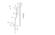
- ハウジング内に配置された複数の半導体光学装置と、
前記ハウジングの壁に配置されたポート部と、
光学的出口である該ポート部に固定して配置されたフェルールと、
該フェルールを通過するとともに該フェルールに固定して取り付けられた複数の光ファイバであって、前記複数の半導体光学装置にそれぞれ光学的に連結された複数の光ファイバと、
を含む、半導体光学装置パッケージ。 - 前記複数の光ファイバの光軸は、互いに対し回転する方向に位置決めされている、請求項1に記載の半導体光学装置パッケージ。
- 前記複数の光ファイバの前記光軸間の前記回転する方向における位置決めの公差は、約−4°から+4°である、請求項2に記載の半導体光学装置パッケージ。
- 前記複数の光ファイバの光軸は、互いに対し側方に位置決めされている、請求項1から3のいずれか1項に記載の半導体光学装置パッケージ。
- 前記複数の光ファイバの前記光軸間の前記側方における位置決めの公差は、約2μm未満である、請求項4に記載の半導体光学装置パッケージ。
- 前記複数の光ファイバは、低融点ガラス、はんだ、及びエポキシ樹脂の少なくとも1つを用いて前記フェルールに固定して取り付けられている、請求項1から5のいずれか1項に記載の半導体光学装置パッケージ。
- 前記複数の光ファイバは、前記複数の半導体光学装置をEDFA増幅器及びラマン増幅器の少なくとも1つに光学的に連結させている、請求項1から6のいずれか1項に記載の半導体光学装置パッケージ。
- 前記半導体光学装置は、半導体レーザ、半導体光ダイオード、少なくとも1つの半導体レーザ、及び少なくとも1つの半導体光ダイオードの少なくとも1つである、請求項1から7のいずれか1項に記載の半導体光学装置パッケージ。
- 前記半導体光学装置の少なくとも1つは、約980nm及び約1480nmの少なくとも1つの波長で発光する、請求項1から8のいずれか1項に記載の半導体光学装置パッケージ。
- 半導体光学装置パッケージの光学出口であるポート部に固定して配置されたフェルールであって、
複数の光ファイバが通過するとともに、該複数の光ファイバが前記フェルールに固定して取り付けられた穴
を含む、フェルール。 - 前記複数の光ファイバの光軸は、互いに対し回転する方向に位置決めされている、請求項10に記載のフェルール。
- 前記複数の光ファイバの前記光軸間の前記回転する方向における位置決めの公差は、約−4°から+4°である、請求項11に記載のフェルール。
- 前記複数の光ファイバの光軸は、互いに対し側方に位置決めされている、請求項10から12のいずれか1項に記載のフェルール。
- 前記複数の光ファイバの前記光軸間の前記側方における位置決めの公差は、約2μm未満である、請求項13に記載のフェルール。
- 前記複数の光ファイバは、低融点ガラス、はんだ、及びエポキシ樹脂の少なくとも1つを用いて前記フェルールに固定して取り付けられている、請求項10から14のいずれか1項に記載のフェルール。
- フェルール、及びフェルールを通過し、該フェルールに固定して取り付けられた複数の光ファイバをハウジングの壁に配置されたポート部を通して挿入するステップと、
前記ハウジング内に配置された複数の半導体光学装置に前記複数の光ファイバを光学的に連結させるステップと、
前記ハウジングの前記壁に前記フェルールを固定して取り付けるステップと、
を含む、半導体光学装置パッケージの製造方法。 - 前記フェルール及び前記複数の光ファイバを前記ポート部を通して挿入する前記ステップ以前に、前記複数の光ファイバを、前記フェルールを通過させて該フェルールに固定して取り付ける、請求項16に記載の方法。
- 前記フェルールに固定して取り付ける前記ステップ以前に、前記複数の光ファイバの光軸を互いに対し回転する方向に位置決めする、請求項17に記載の方法。
- 前記フェルールに固定して取り付ける前記ステップ以前に、前記複数の光ファイバの光軸を互いに対し側方に位置決めする、請求項17に記載の方法。
- 前記複数の光ファイバは、前記複数の半導体光学装置をEDFA増幅器及びラマン増幅器の少なくとも1つに光学的に連結させる、請求項16から19のいずれか1項に記載の方法。
- 前記半導体光学装置は、半導体レーザ、半導体光ダイオード、少なくとも1つの半導体レーザ、及び少なくとも1つの半導体光ダイオードの少なくとも1つである、請求項16から20のいずれか1項に記載の方法。
Applications Claiming Priority (3)
| Application Number | Priority Date | Filing Date | Title |
|---|---|---|---|
| US25067709P | 2009-10-12 | 2009-10-12 | |
| US61/250,677 | 2009-10-12 | ||
| PCT/IB2010/001909 WO2011045633A1 (en) | 2009-10-12 | 2010-08-02 | Co-packaged semiconductor optical devices |
Publications (2)
| Publication Number | Publication Date |
|---|---|
| JP2013507665A true JP2013507665A (ja) | 2013-03-04 |
| JP2013507665A5 JP2013507665A5 (ja) | 2014-02-27 |
Family
ID=43384564
Family Applications (1)
| Application Number | Title | Priority Date | Filing Date |
|---|---|---|---|
| JP2012533704A Pending JP2013507665A (ja) | 2009-10-12 | 2010-08-02 | 共同パッケージ化された半導体光学装置 |
Country Status (5)
| Country | Link |
|---|---|
| US (1) | US20120213480A1 (ja) |
| EP (1) | EP2488906A1 (ja) |
| JP (1) | JP2013507665A (ja) |
| CN (2) | CN201974549U (ja) |
| WO (1) | WO2011045633A1 (ja) |
Families Citing this family (4)
| Publication number | Priority date | Publication date | Assignee | Title |
|---|---|---|---|---|
| WO2011045633A1 (en) * | 2009-10-12 | 2011-04-21 | Oclaro Technology Limited | Co-packaged semiconductor optical devices |
| GB2488849A (en) * | 2011-02-25 | 2012-09-12 | Oclaro Technology Ltd | Optical path switching with Raman amplification |
| US9503181B2 (en) | 2015-01-06 | 2016-11-22 | Ii-Vi Incorporated | Rare earth-doped fiber amplifier with integral optical metrology functionality |
| CN107735705A (zh) | 2015-06-18 | 2018-02-23 | 康宁股份有限公司 | 用于使激光二极管与光纤光学耦合的光学耦合系统 |
Citations (7)
| Publication number | Priority date | Publication date | Assignee | Title |
|---|---|---|---|---|
| JPH11258453A (ja) * | 1998-03-12 | 1999-09-24 | Fujitsu Ltd | 偏光合成装置および偏光分離装置ならびに励起光出力装置 |
| JP2001021750A (ja) * | 1999-07-12 | 2001-01-26 | Furukawa Electric Co Ltd:The | 光合分波モジュール |
| JP2001100066A (ja) * | 1999-07-23 | 2001-04-13 | Furukawa Electric Co Ltd:The | 光部品およびその製造方法 |
| US20020096498A1 (en) * | 2001-01-25 | 2002-07-25 | Murdza Randal A. | System and process for magnetic fixturing of optical components on bench for solder attach |
| JP2002258076A (ja) * | 2001-03-01 | 2002-09-11 | Hitachi Cable Ltd | 導波路型光合分波器 |
| JP2004252423A (ja) * | 2003-01-31 | 2004-09-09 | Fuji Photo Film Co Ltd | ファイバモジュールおよびその製造方法 |
| JP2008032835A (ja) * | 2006-07-26 | 2008-02-14 | Fujitsu Ltd | 光デバイスおよびその製造方法 |
Family Cites Families (11)
| Publication number | Priority date | Publication date | Assignee | Title |
|---|---|---|---|---|
| JPH0677564A (ja) * | 1992-08-24 | 1994-03-18 | Hitachi Cable Ltd | 光源モジュール |
| JPH0792342A (ja) * | 1993-07-29 | 1995-04-07 | Sumitomo Electric Ind Ltd | 光導波路モジュール |
| US6540411B1 (en) * | 1999-06-15 | 2003-04-01 | Jds Uniphase Inc. | Optical coupling |
| US6513991B1 (en) * | 2000-01-28 | 2003-02-04 | Agere Systems, Inc. | Semiconductor optical device package |
| US20020110328A1 (en) * | 2001-02-14 | 2002-08-15 | Bischel William K. | Multi-channel laser pump source for optical amplifiers |
| US6782146B2 (en) * | 2001-09-28 | 2004-08-24 | Corning Incorporated | Multiple polarization combiner-splitter-isolator and method of manufacturing the same |
| US7039271B2 (en) * | 2002-11-27 | 2006-05-02 | Oplink Communications, Inc. | Reduced element optical add-drop multiplexer |
| US20040184753A1 (en) * | 2003-01-31 | 2004-09-23 | Fuji Photo Film Co., Ltd. | Fiber module in which optical fiber coated with metal or inorganic material is fixed to sealable package so that an end of the optical fiber appears inside the package |
| JP4008421B2 (ja) * | 2004-02-24 | 2007-11-14 | 株式会社デンソー | 光ファイバ接続構造 |
| US7128476B1 (en) * | 2004-08-20 | 2006-10-31 | The United States Of America As Represented By The National Security Agency | Photonic integrated circuit and method of fabricating same |
| WO2011045633A1 (en) * | 2009-10-12 | 2011-04-21 | Oclaro Technology Limited | Co-packaged semiconductor optical devices |
-
2010
- 2010-08-02 WO PCT/IB2010/001909 patent/WO2011045633A1/en not_active Ceased
- 2010-08-02 JP JP2012533704A patent/JP2013507665A/ja active Pending
- 2010-08-02 US US13/501,359 patent/US20120213480A1/en not_active Abandoned
- 2010-08-02 EP EP10754988A patent/EP2488906A1/en not_active Withdrawn
- 2010-09-19 CN CN2010205361732U patent/CN201974549U/zh not_active Expired - Lifetime
- 2010-09-19 CN CN2010102881833A patent/CN102043210A/zh active Pending
Patent Citations (7)
| Publication number | Priority date | Publication date | Assignee | Title |
|---|---|---|---|---|
| JPH11258453A (ja) * | 1998-03-12 | 1999-09-24 | Fujitsu Ltd | 偏光合成装置および偏光分離装置ならびに励起光出力装置 |
| JP2001021750A (ja) * | 1999-07-12 | 2001-01-26 | Furukawa Electric Co Ltd:The | 光合分波モジュール |
| JP2001100066A (ja) * | 1999-07-23 | 2001-04-13 | Furukawa Electric Co Ltd:The | 光部品およびその製造方法 |
| US20020096498A1 (en) * | 2001-01-25 | 2002-07-25 | Murdza Randal A. | System and process for magnetic fixturing of optical components on bench for solder attach |
| JP2002258076A (ja) * | 2001-03-01 | 2002-09-11 | Hitachi Cable Ltd | 導波路型光合分波器 |
| JP2004252423A (ja) * | 2003-01-31 | 2004-09-09 | Fuji Photo Film Co Ltd | ファイバモジュールおよびその製造方法 |
| JP2008032835A (ja) * | 2006-07-26 | 2008-02-14 | Fujitsu Ltd | 光デバイスおよびその製造方法 |
Also Published As
| Publication number | Publication date |
|---|---|
| WO2011045633A1 (en) | 2011-04-21 |
| EP2488906A1 (en) | 2012-08-22 |
| US20120213480A1 (en) | 2012-08-23 |
| CN201974549U (zh) | 2011-09-14 |
| CN102043210A (zh) | 2011-05-04 |
Similar Documents
| Publication | Publication Date | Title |
|---|---|---|
| US6765935B2 (en) | Semiconductor laser module, manufacturing method thereof and optical amplifier | |
| CN109716599B (zh) | 具有波分复用器、隔离器、抽头滤波器和光电探测器的光纤耦合激光源泵 | |
| JP6857127B2 (ja) | 光増幅器モジュール | |
| US6782028B2 (en) | Semiconductor laser device for use in a semiconductor laser module and an optical amplifier | |
| US8588267B1 (en) | Rectangular core optical fiber and rectangular core optical fiber arrays | |
| KR101896697B1 (ko) | 다채널 광 모듈 및 그의 제조 방법 | |
| US6310717B1 (en) | Optical amplifier and fiber module for optical amplification | |
| JP2012238781A (ja) | Yb添加ガラスファイバを用いるファイバレーザ発振器およびファイバレーザ増幅器 | |
| JP2013507665A (ja) | 共同パッケージ化された半導体光学装置 | |
| CN103197383A (zh) | 阵列定向光耦合装置 | |
| JP2013507665A5 (ja) | ||
| CN104678517B (zh) | 一种集成的半导体光学器件 | |
| US20150146757A1 (en) | Semiconductor laser module | |
| JP5028503B2 (ja) | 光モジュール | |
| US6381066B1 (en) | Integrated semiconductor optical amplifier system | |
| CN118295086B (zh) | 具有波分复用器的光纤耦合激光源泵浦 | |
| EP3679425A1 (en) | Micro-optical bench architecture for master oscillator power amplifier (mopa) | |
| US20020105984A1 (en) | Integrated laser beam synthesizing module for use in a semiconductor laser module and an optical amplifier | |
| WO2018097241A1 (ja) | レーザ装置及び光源装置 | |
| CN204556906U (zh) | 基于可调光衰减器集成的半导体光学器件 | |
| CN204613454U (zh) | 基于半导体激光器集成的半导体光学器件 | |
| TWI667506B (zh) | 具有高輸出功率的光源裝置 | |
| US20020094590A1 (en) | Method for manufacturing semiconductor laser module, semiconductor laser module and Raman amplifier | |
| KR20140086033A (ko) | 광원 모듈의 광섬유 고정 장치 및 방법 | |
| KR101909159B1 (ko) | 광섬유 결합형 다중 광원 광 모듈 및 이의 제조 방법 |
Legal Events
| Date | Code | Title | Description |
|---|---|---|---|
| A977 | Report on retrieval |
Free format text: JAPANESE INTERMEDIATE CODE: A971007 Effective date: 20130628 |
|
| A131 | Notification of reasons for refusal |
Free format text: JAPANESE INTERMEDIATE CODE: A131 Effective date: 20130702 |
|
| A601 | Written request for extension of time |
Free format text: JAPANESE INTERMEDIATE CODE: A601 Effective date: 20131001 |
|
| A602 | Written permission of extension of time |
Free format text: JAPANESE INTERMEDIATE CODE: A602 Effective date: 20131008 |
|
| A524 | Written submission of copy of amendment under article 19 pct |
Free format text: JAPANESE INTERMEDIATE CODE: A524 Effective date: 20140106 |
|
| A131 | Notification of reasons for refusal |
Free format text: JAPANESE INTERMEDIATE CODE: A131 Effective date: 20140708 |
|
| A02 | Decision of refusal |
Free format text: JAPANESE INTERMEDIATE CODE: A02 Effective date: 20141202 |