JP2014016830A - Power estimation support program, power estimation support device, and power estimation support method - Google Patents
Power estimation support program, power estimation support device, and power estimation support method Download PDFInfo
- Publication number
- JP2014016830A JP2014016830A JP2012154068A JP2012154068A JP2014016830A JP 2014016830 A JP2014016830 A JP 2014016830A JP 2012154068 A JP2012154068 A JP 2012154068A JP 2012154068 A JP2012154068 A JP 2012154068A JP 2014016830 A JP2014016830 A JP 2014016830A
- Authority
- JP
- Japan
- Prior art keywords
- signal
- cell
- information
- data
- circuit
- Prior art date
- Legal status (The legal status is an assumption and is not a legal conclusion. Google has not performed a legal analysis and makes no representation as to the accuracy of the status listed.)
- Granted
Links
Images










Abstract
【課題】レジスタ転送レベルの検証環境における電力パラメータの抽出を可能にすることにより、回路の消費電力の見積もりを支援すること。
【解決手段】電力見積支援装置100は、マッピング情報101を参照して、ネットリストNL上の観測信号を出力する第1のセルを起点として前段のセルを順次辿ることにより、RTL設計データRDの信号と対応関係を有するネットリストNLの信号が入力される第2のセルを検出する。電力見積支援装置100は、検出した第2のセルから第1のセルまでの部分回路をネットリストNLの中から抽出することにより、RTL設計データRDとネットリストNLとの差分を表す差分回路情報を作成する。電力見積支援装置100は、第2のセルに入力されるネットリストNLの信号と対応関係を有するRTL設計データRDの信号の信号名と、第2のセルとを対応付けて表す信号情報を作成する。
【選択図】図1An object of the present invention is to support estimation of power consumption of a circuit by enabling extraction of power parameters in a verification environment of a register transfer level.
A power estimation support apparatus (100) refers to mapping information (101) and sequentially traces cells in the previous stage starting from a first cell that outputs an observation signal on a netlist (NL), thereby generating RTL design data (RD). A second cell to which a signal of a netlist NL having a correspondence relationship with the signal is input is detected. The power estimation support apparatus 100 extracts difference circuit information representing the difference between the RTL design data RD and the netlist NL by extracting the partial circuits from the detected second cell to the first cell from the netlist NL. Create The power estimation support apparatus 100 creates signal information in which the signal name of the signal of the RTL design data RD having a correspondence relationship with the signal of the netlist NL input to the second cell is associated with the second cell. To do.
[Selection] Figure 1
Description
本発明は、電力見積支援プログラム、電力見積支援装置および電力見積支援方法に関する。 The present invention relates to a power estimation support program, a power estimation support apparatus, and a power estimation support method.
従来、ゲートレベルを対象として被評価回路の消費電力を見積もる場合、例えば、消費電力の見積りに必要となる電力パラメータを抽出するために、論理合成後のネットリストやレイアウト後のネットリストを用いた機能検証が行われる。 Conventionally, when estimating the power consumption of a circuit to be evaluated for the gate level, for example, a netlist after logic synthesis or a netlist after layout has been used to extract a power parameter necessary for estimating the power consumption. Functional verification is performed.
関連する先行技術としては、例えば、エミュレータやFPGA(Field Programmable Gate Array)ボードを用いて、電力用の観測ポイントのデータを抽出するものがある。また、対象回路内の観測対象の信号をグルーピングして、複数の観測対象の動作回数を算出する計測回路を採用する技術がある。 As a related prior art, for example, there is a technique of extracting observation point data for power using an emulator or an FPGA (Field Programmable Gate Array) board. In addition, there is a technology that employs a measurement circuit that groups signals to be observed in a target circuit and calculates the number of operations of a plurality of observation targets.
しかしながら、従来技術では、消費電力の見積りに必要となる電力パラメータを抽出するために、被評価回路のネットリストを用いた機能検証を行う場合、RTL(Register Transfer Level)の検証環境では正常に動作しない場合がある。また、被評価回路のゲートレベルでの機能検証を行うための検証環境を新たに構築する場合は検証者の作業負荷が増大するという問題がある。 However, in the prior art, when function verification using the net list of the circuit to be evaluated is performed in order to extract a power parameter necessary for estimating power consumption, it operates normally in an RTL (Register Transfer Level) verification environment. May not. Further, when a new verification environment for performing functional verification at the gate level of the circuit to be evaluated is constructed, there is a problem that the workload of the verifier increases.
本発明は、上述した従来技術による問題点を解消するため、レジスタ転送レベルの検証環境における電力パラメータの抽出を可能にすることにより、回路の消費電力の見積もりを支援することができる電力見積支援プログラム、電力見積支援装置および電力見積支援方法を提供することを目的とする。 The present invention eliminates the problems caused by the prior art described above, and enables the estimation of power consumption of a circuit by enabling extraction of power parameters in a register transfer level verification environment. An object of the present invention is to provide a power estimation support apparatus and a power estimation support method.
上述した課題を解決し、目的を達成するため、本発明の一側面によれば、消費電力の見積対象となる対象回路のネットリストの信号名とレジスタ転送レベルで記述された前記対象回路の設計情報の信号名との対応関係を表すマッピング情報を取得し、前記ネットリストの中から信号値の変化の観測対象となる観測信号を選択し、取得した前記マッピング情報を参照して、前記ネットリスト上の選択した前記観測信号を出力する第1のセルを起点として前段のセルを順次辿ることにより、前記設計情報の信号と対応関係を有する前記ネットリストの信号が入力される第2のセルを検出し、検出した前記第2のセルから前記第1のセルまでの部分回路を前記ネットリストの中から抽出することにより、前記設計情報と前記ネットリストとの差分を表す差分回路情報を作成し、前記第2のセルに入力される前記ネットリストの信号と対応関係を有する前記設計情報の信号の信号名と、前記第2のセルとを対応付けて表す信号情報を作成し、作成した前記差分回路情報と前記信号情報とを関連付けて出力する電力見積支援プログラム、電力見積支援装置および電力見積支援方法が提案される。 In order to solve the above-described problems and achieve the object, according to one aspect of the present invention, the design of the target circuit described by the netlist signal name and the register transfer level of the target circuit whose power consumption is to be estimated Obtaining mapping information representing a correspondence relationship with signal names of information, selecting an observation signal to be observed for a change in signal value from the net list, referring to the obtained mapping information, and The second cell to which the netlist signal having the correspondence with the design information signal is input by sequentially tracing the preceding cell starting from the first cell that outputs the observed signal selected above. And detecting a difference between the design information and the netlist by extracting a partial circuit from the second cell to the first cell detected from the netlist. Signal information that creates difference circuit information and associates the signal name of the design information signal that has a corresponding relationship with the netlist signal input to the second cell and the second cell. A power estimation support program, a power estimation support device, and a power estimation support method are proposed in which the generated difference circuit information and the signal information are output in association with each other.
本発明の一側面によれば、レジスタ転送レベルの検証環境における電力パラメータの抽出を可能にすることにより、回路の消費電力の見積もりを支援することができるという効果を奏する。 According to one aspect of the present invention, it is possible to support estimation of power consumption of a circuit by enabling extraction of power parameters in a register transfer level verification environment.
以下に添付図面を参照して、この発明にかかる電力見積支援プログラム、電力見積支援装置および電力見積支援方法の実施の形態を詳細に説明する。 Exemplary embodiments of a power estimation support program, a power estimation support apparatus, and a power estimation support method according to the present invention will be described below in detail with reference to the accompanying drawings.
(電力見積支援方法の一実施例)
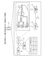
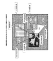
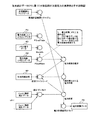
図1は、実施の形態にかかる電力見積支援方法の一実施例を示す説明図である。図1において、電力見積支援装置100は、対象回路の消費電力の見積もりを支援するコンピュータである。
(One example of power estimation support method)
FIG. 1 is an explanatory diagram of an example of a power estimation support method according to the embodiment. In FIG. 1, a power
対象回路は、消費電力の見積もり対象となる回路であり、例えば、LSI(Large Scale Integrated circuit)である。対象回路の回路情報は、RTL設計データ、論理合成後のネットリスト、レイアウト後のネットリストと設計が進むにつれて詳細度が上がる傾向にある。また、対象回路の回路情報は、対象回路に新たな機能が追加されるなどして変化する場合がある。 The target circuit is a circuit whose power consumption is to be estimated, and is, for example, an LSI (Large Scale Integrated circuit). The circuit information of the target circuit tends to increase in detail as the design proceeds with RTL design data, a netlist after logic synthesis, and a netlist after layout. The circuit information of the target circuit may change due to a new function added to the target circuit.
ここで、RTL設計データ(以下、「RTL設計データRD」という)は、RTLで記述された対象回路の回路情報である。エミュレーションやHDL(Hardware Description Language)ソフトウェアシミュレータでは、例えば、論理合成可能なデータの集合を用いてシミュレーションする。すなわち、RTL設計データRDは、エミュレーションまたはHDLシミュレーションが可能かつ論理合成が可能な回路情報である。 Here, the RTL design data (hereinafter referred to as “RTL design data RD”) is circuit information of a target circuit described in RTL. In an emulation or HDL (Hardware Description Language) software simulator, for example, simulation is performed using a set of data that can be logically synthesized. That is, the RTL design data RD is circuit information that can be emulated or HDL simulated and can be logically synthesized.
また、ネットリストは、対象回路内のセル間の接続関係を表す情報である。セルは、例えば、NOTゲート、ANDゲート、配線、バッファ、INV(インバータ)、FF(フリップフロップ)などの回路素子である。具体的には、例えば、ネットリストは、RTL設計データRDを論理合成して変換した変換後の設計データ、あるいは、変換後の設計データをレイアウト工程において加工した設計データである。以下の説明では、「ネットリストNL」と表記した場合、対象回路のレイアウト後のネットリストを表すものとする。 The net list is information representing the connection relationship between cells in the target circuit. The cell is, for example, a circuit element such as a NOT gate, an AND gate, a wiring, a buffer, INV (inverter), and FF (flip-flop). Specifically, for example, the netlist is converted design data obtained by logically synthesizing and converting RTL design data RD, or design data obtained by processing the converted design data in a layout process. In the following description, the notation “net list NL” represents the net list after the layout of the target circuit.
RTL設計データRDの信号の波形データは、エミュレーションでの被検証データとなる。一方、対象回路の消費電力の見積もりを高精度に行う場合、消費電力の見積りに用いる波形データは、論理合成後のネットリストやレイアウト後のネットリストの信号の波形データであることが望ましい。 The waveform data of the signal of the RTL design data RD becomes data to be verified in emulation. On the other hand, when the power consumption of the target circuit is estimated with high accuracy, the waveform data used for the power consumption estimation is desirably the waveform data of the netlist after logic synthesis or the netlist signal after layout.
また、シミュレーションまたはエミュレーションのいずれであっても、検証環境を作成するのはRTLに限られることが多い。このため、電力見積もりのためのゲートレベルのシミュレーションを行う場合、ゲートレベルの検証環境の構築が電力見積もりのための追加工数となってしまう。 Further, in either simulation or emulation, the creation of the verification environment is often limited to the RTL. For this reason, when performing a gate level simulation for power estimation, the construction of a gate level verification environment is an additional man-hour for power estimation.
そこで、本実施の形態では、電力見積支援装置100は、RTL設計データRD上の信号に対応するネットリストNL上の信号が入力されるセルから、観測対象となる信号を出力するセルまでのパスをRTLとの差分回路として抽出する。これにより、RTL用の検証環境での電力見積に必要な電力パラメータの抽出を可能にする。以下、電力見積支援装置100の電力見積支援処理の処理手順の一例について説明する。
Therefore, in the present embodiment, power
(1)電力見積支援装置100は、対象回路のRTL設計データRDとネットリストNLとを取得する。具体的には、例えば、電力見積支援装置100は、ユーザの操作入力により、対象回路のRTL設計データRDとネットリストNLとを取得することにしてもよい。
(1) The power
(2)電力見積支援装置100は、取得したRTL設計データRDとネットリストNLとに基づいて、マッピング情報101を作成する。マッピング情報101は、ネットリストNLの信号名とRTL設計データRDの信号名との対応関係を表す情報である。具体的には、例えば、マッピング情報101は、RTL設計データRDとネットリストNLとの間で同一の信号線を指す信号の対応関係を表すものである。
(2) The power
図1の例では、マッピング情報101には、ネットリストNLの信号名「A」とRTL設計データRDの信号名「a」との対応関係が表されている。また、ネットリストNLの信号名「B」とRTL設計データRDの信号名「b」との対応関係が表されている。ネットリストNLの信号名「C」とRTL設計データRDの信号名「c」との対応関係が表されている。
In the example of FIG. 1, the
(3)電力見積支援装置100は、ネットリストNLの中から信号値の変化の観測対象となる観測信号を選択する。観測信号は、例えば、対象回路の消費電力の要因となるセルから出力されるクロック信号やデータ信号である。具体的には、例えば、観測信号は、CGIC(クロックゲーティングインテグレイティッドセル)から出力される信号やトグルレートが変化するセルから出力される信号などである。
(3) The power
CGICは、供給先へのクロック信号の供給を一時的に停止するセルである。CGICによれば、例えば、クロック信号の供給先となるFFの入力が変化しない場合に、そのFFへのクロック信号の供給を一時的に停止することにより、対象回路の消費電力を削減することができる。また、トグルレートは、信号の信号値が変化した単位時間当たりの回数を表すものである。 The CGIC is a cell that temporarily stops the supply of the clock signal to the supply destination. According to CGIC, for example, when the input of the FF that is the supply destination of the clock signal does not change, the power consumption of the target circuit can be reduced by temporarily stopping the supply of the clock signal to the FF. it can. The toggle rate represents the number of times per unit time that the signal value of the signal has changed.
すなわち、CGICから出力される信号やトグルレートが変化するセルから出力される信号の波形データは、対象回路の消費電力を見積もる際の重要な指標となる。このため、電力見積支援装置100は、CGICから出力される信号やトグルレートが変化するセルから出力される信号を観測信号として選択することにしてもよい。
That is, the waveform data of the signal output from the CGIC and the signal output from the cell whose toggle rate changes is an important index when estimating the power consumption of the target circuit. For this reason, the power
図1の例では、ネットリストNLに基づく対象回路に含まれるセルC1〜C6が表示されている。そして、対象回路内のセルC6から出力される信号sigが観測信号として選択されている。ただし、図面では、対象回路の一部を抜粋して表示している。 In the example of FIG. 1, cells C1 to C6 included in the target circuit based on the netlist NL are displayed. Then, the signal sig output from the cell C6 in the target circuit is selected as the observation signal. However, in the drawing, a part of the target circuit is extracted and displayed.
(4)電力見積支援装置100は、作成したマッピング情報101を参照して、ネットリストNL上の選択した観測信号を出力する第1のセルを起点として前段のセルを順次辿る。これにより、電力見積支援装置100は、RTL設計データRDの信号と対応関係を有するネットリストNLの信号が入力される第2のセルを検出する。
(4) The power
図1の例では、ネットリストNLのセルC1に入力される信号の信号名「A」とRTL設計データRDの信号名「a」とが対応している。また、ネットリストNLのセルC2に入力される信号の信号名「B」とRTL設計データRDの信号名「b」とが対応している。ネットリストNLのセルC3に入力される信号の信号名「C」とRTL設計データRDの信号名「c」とが対応している。また、セルC6から出力される信号sigが観測信号として選択されているため、セルC6が第1のセルとなる。このため、セルC6を起点として前段のセルを順次辿ることにより、セルC1、セルC2およびセルC3が第2のセルとして検出される。 In the example of FIG. 1, the signal name “A” of the signal input to the cell C1 of the netlist NL corresponds to the signal name “a” of the RTL design data RD. The signal name “B” of the signal input to the cell C2 of the netlist NL corresponds to the signal name “b” of the RTL design data RD. The signal name “C” of the signal input to the cell C3 of the netlist NL corresponds to the signal name “c” of the RTL design data RD. In addition, since the signal sig output from the cell C6 is selected as the observation signal, the cell C6 becomes the first cell. For this reason, the cell C1, the cell C2, and the cell C3 are detected as the second cell by sequentially tracing the preceding cells starting from the cell C6.
(5)電力見積支援装置100は、検出した第2のセルから第1のセルまでの部分回路をネットリストNLの中から抽出することにより、RTL設計データRDとネットリストNLとの差分を表す差分回路情報を作成する。図1の例では、セルC1〜C6を含む部分回路102を表す差分回路情報103が作成される。
(5) The power
(6)電力見積支援装置100は、第2のセルに入力されるネットリストNLの信号と対応関係を有するRTL設計データRDの信号の信号名と、第2のセルとを対応付けて表す信号情報を作成する。具体的には、例えば、信号情報は、RTL設計データRDとネットリストNLとの差分を表す部分回路の入力端子と、該入力端子に入力される信号と対応関係を有するRTL設計データRDの信号の信号名とを対応付けて表す情報である。図1の例では、信号情報104が作成されている。
(6) The power
ここで、セルC1に入力されるネットリストNLの信号(信号名「A」)と対応関係を有するRTL設計データRDの信号の信号名は「a」である。また、セルC2に入力されるネットリストNLの信号(信号名「B」)と対応関係を有するRTL設計データRDの信号の信号名は「b」である。また、セルC3に入力されるネットリストNLの信号(信号名「C」)と対応関係を有するRTL設計データRDの信号の信号名は「c」である。 Here, the signal name of the signal of the RTL design data RD having a correspondence relationship with the signal (signal name “A”) of the netlist NL input to the cell C1 is “a”. Further, the signal name of the signal of the RTL design data RD having a correspondence relation with the signal (signal name “B”) of the netlist NL input to the cell C2 is “b”. Further, the signal name of the signal of the RTL design data RD that has a corresponding relationship with the signal (signal name “C”) of the netlist NL input to the cell C3 is “c”.
このため、信号情報104は、RTL設計データRDの信号の信号名「a」とセルC1とを対応付けて表す信号情報を含む。また、信号情報104は、RTL設計データRDの信号の信号名「b」とセルC2とを対応付けて表す信号情報を含む。また、信号情報104は、RTL設計データRDの信号の信号名「c」とセルC3とを対応付けて表す信号情報を含む。
For this reason, the
(7)電力見積支援装置100は、作成した差分回路情報と信号情報とを関連付けて出力する。図1の例では、差分回路情報103と信号情報104とが関連付けて出力されることになる。
(7) The power
以上説明した、本実施の形態にかかる電力見積支援装置100によれば、RTL設計データRDとネットリストNLとの差分を表す差分回路情報を作成することができる。また、電力見積支援装置100によれば、第2のセルに入力されるネットリストNLの信号と対応関係を有するRTL設計データRDの信号の信号名と、第2のセルとを対応付けて表す信号情報を作成することができる。
According to the power
これにより、例えば、部分回路102の各入力端子に入力される信号と対応関係を有するRTL設計データRDの信号の信号名「a,b,c」を特定することができる。このため、RTL用のテストベンチにおいて、RTL設計データRDと部分回路102とを適切に接続することができるようになる。
Thereby, for example, the signal name “a, b, c” of the signal of the RTL design data RD having a correspondence relationship with the signal input to each input terminal of the
すなわち、RTL設計データRDと差分回路情報103とをRTL用のテストベンチに与えることにより、対象回路の論理シミュレーションの実行が可能となる。この結果、対象回路の消費電力を見積もる際の重要な指標となる信号、例えば、RTL設計データRDからは推測が難しい信号の波形データを取得可能となり、対象回路の電力見積もりを支援することができる。
That is, by giving the RTL design data RD and the
以下の説明では、図1に示した電力見積支援装置100を、対象回路の消費電力を見積もる電力見積装置200に適用した場合について説明する。
In the following description, the case where the power
(電力見積装置200のハードウェア構成例)
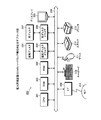
図2は、電力見積装置200のハードウェア構成例を示すブロック図である。図2において、電力見積装置200は、CPU(Central Processing Unit)201と、ROM(Read‐Only Memory)202と、RAM(Random Access Memory)203と、磁気ディスクドライブ204と、磁気ディスク205と、光ディスクドライブ206と、光ディスク207と、ディスプレイ208と、I/F(Interface)209と、キーボード210と、マウス211と、スキャナ212と、プリンタ213と、を有している。また、各構成部はバス200によってそれぞれ接続されている。
(Hardware configuration example of power estimation apparatus 200)
FIG. 2 is a block diagram illustrating a hardware configuration example of the
ここで、CPU201は、電力見積装置200の全体の制御を司る。ROM202は、ブートプログラムなどのプログラムを記憶している。RAM203は、CPU201のワークエリアとして使用される。磁気ディスクドライブ204は、CPU201の制御にしたがって磁気ディスク205に対するデータのリード/ライトを制御する。磁気ディスク205は、磁気ディスクドライブ204の制御で書き込まれたデータを記憶する。
Here, the
光ディスクドライブ206は、CPU201の制御にしたがって光ディスク207に対するデータのリード/ライトを制御する。光ディスク207は、光ディスクドライブ206の制御で書き込まれたデータを記憶したり、光ディスク207に記憶されたデータをコンピュータに読み取らせたりする。
The
ディスプレイ208は、カーソル、アイコンあるいはツールボックスをはじめ、文書、画像、機能情報などのデータを表示する。このディスプレイ208は、例えば、CRT、TFT液晶ディスプレイ、プラズマディスプレイなどを採用することができる。 The display 208 displays data such as a document, an image, and function information as well as a cursor, an icon, or a tool box. As the display 208, for example, a CRT, a TFT liquid crystal display, a plasma display, or the like can be adopted.
I/F209は、通信回線を通じてLAN(Local Area Network)、WAN(Wide Area Network)、インターネットなどのネットワーク214に接続され、このネットワーク214を介して他の装置に接続される。そして、I/F209は、ネットワーク214と内部のインターフェースを司り、外部装置からのデータの入出力を制御する。I/F209には、例えば、モデムやLANアダプタなどを採用することができる。
The I /
キーボード210は、文字、数字、各種指示などの入力のためのキーを備え、データの入力を行う。また、タッチパネル式の入力パッドやテンキーなどであってもよい。マウス211は、カーソルの移動や範囲選択、あるいはウィンドウの移動やサイズの変更などを行う。ポインティングデバイスとして同様に機能を備えるものであれば、トラックボールやジョイスティックなどであってもよい。
The
スキャナ212は、画像を光学的に読み取り、電力見積装置200内に画像データを取り込む。なお、スキャナ212は、OCR(Optical Character Reader)機能を持たせてもよい。また、プリンタ213は、画像データや文書データを印刷する。プリンタ213には、例えば、レーザプリンタやインクジェットプリンタを採用することができる。
The
なお、電力見積装置200は、上述した構成部のうち、例えば、光ディスクドライブ206、光ディスク207、スキャナ212、プリンタ213等を有していなくてもよい。
Note that the
(電力見積装置200の機能的構成例)
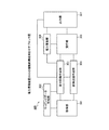
つぎに、電力見積装置200の機能的構成例について説明する。図3は、電力見積装置200の機能的構成例を示すブロック図である。図3において、電力見積装置200は、取得部301と、マッピングデータ作成部302と、差分回路作成部303と、計測回路作成部304と、実行部305と、電力算出部306と、出力部307と、を含む構成である。取得部301〜出力部307は制御部となる機能であり、具体的には、例えば、図2に示したROM202、RAM203、磁気ディスク205、光ディスク207などの記憶装置に記憶されたプログラムをCPU201に実行させることにより、または、I/F209により、その機能を実現する。また、各機能部の処理結果は、例えば、RAM203、磁気ディスク205、光ディスク207などの記憶装置に記憶される。
(Functional configuration example of power estimation apparatus 200)
Next, a functional configuration example of the
取得部301は、対象回路のRTL設計データRDを取得する機能を有する。また、取得部301は、対象回路のネットリストNLを取得する機能を有する。具体的には、例えば、取得部301は、図2に示したキーボード210やマウス211を用いたユーザの操作入力により、RTL設計データRDおよびネットリストNLを取得する。
The
また、取得部301は、例えば、ネットワーク214を介して、外部のコンピュータからRTL設計データRDおよびネットリストNLを取得することにしてもよい。なお、取得部301は、例えば、取得したRTL設計データRDを論理合成することにより、ネットリストNLを取得することにしてもよい。ただし、この場合、ネットリストNLは、レイアウト前のネットリストとなる。
The
マッピングデータ作成部302は、対象回路のRTL設計データRDとネットリストNLとの間で同一の信号線を指す信号の対応関係を表すマッピングデータMDを作成する機能を有する。具体的には、例えば、マッピングデータ作成部302は、RTL設計データRDとネットリストNTを等価性検証ツールに与えて、ネットリストNLの信号名に一致するRTL設計データRDの信号名を検出することによりマッピングデータMDを作成する。なお、マッピングデータMDは、図1に示したマッピング情報101に相当する。
The mapping
また、マッピングデータ作成部302は、論理合成ツールおよびユーザ定義による設計ルールにより、マッピングデータMDを作成することにしてもよい。例えば、RTL設計データRDのFFになる信号線名とネットリストNLの中の信号線名「+_reg」というFFの出力端子が対応するというルールがあれば、この対応関係を表す情報が作成される。ここで、マッピングデータMDの具体例について説明する。
Further, the mapping
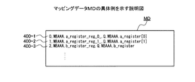
図4は、マッピングデータMDの具体例を示す説明図である。図4において、マッピングデータMDは、対象回路のRTL設計データRDとネットリストNLとの間で同一の信号線を指す信号の対応関係を表す対応情報(例えば、対応情報400−1〜400−3)を有している。各対応情報には、CSV(Comma Separated Values)形式により、ネットリストNLの信号名に対応するRTL設計データRDの信号名が記述されている。 FIG. 4 is an explanatory diagram showing a specific example of the mapping data MD. In FIG. 4, the mapping data MD is correspondence information (for example, correspondence information 400-1 to 400-3) indicating a correspondence relationship between signals indicating the same signal line between the RTL design data RD of the target circuit and the netlist NL. )have. In each correspondence information, the signal name of the RTL design data RD corresponding to the signal name of the netlist NL is described in CSV (Comma Separated Values) format.
例えば、対応情報400−1によれば、対象回路のネットリストNLの信号名「MBAAA.a_register_req_0_.Q」とRTL設計データRDの信号名「MBAAA.a_register[0]」との対応関係を特定することができる。 For example, according to the correspondence information 400-1, the correspondence between the signal name “MBAAA.a_register_req_0_.Q” of the netlist NL of the target circuit and the signal name “MBAAAA.a_register [0]” of the RTL design data RD is specified. be able to.
図3の説明に戻り、差分回路作成部303は、ネットリストNLとマッピングデータMDとに基づいて、差分回路を作成する機能を有する。ここで、差分回路とは、RTL設計データRDとネットリストNLとの差分を表す部分回路である。
Returning to the description of FIG. 3, the difference
具体的には、例えば、差分回路作成部303は、対象回路の基礎データを作成する。ここで、基礎データとは、対象回路の論理シミュレーションや電力見積もりに用いられる情報である。基礎データは、例えば、後述するコンフィギュレーションデータCGと差分回路データDFとを含む。
Specifically, for example, the difference
コンフィギュレーションデータCGは、クロック起点データCKDと、計算範囲IDマップデータEDと、クロック起点親子関係データFDと、メモリ端子データMDと、非クロックツリー観測ポイントデータODと、電力係数(ユニットセル)データPUと、電力係数(メモリ)データPMと、差分回路コンフィギュレーションデータDCGと、を含むファイル群である。基礎データの作成例については、図5〜図21を用いて後述する。 The configuration data CG includes clock start data CKD, calculation range ID map data ED, clock start parent-child relationship data FD, memory terminal data MD, non-clock tree observation point data OD, and power coefficient (unit cell) data. A file group including a PU, power coefficient (memory) data PM, and difference circuit configuration data DCG. An example of creating basic data will be described later with reference to FIGS.
計測回路作成部304は、観測信号の信号値の変化を計測する計測回路を作成する機能を有する。ここで、観測信号は、上述したように、対象回路の消費電力の要因となるセルから出力される信号である。計測回路は、例えば、観測信号の信号値が変化した回数を計測する回路である。すなわち、計測回路は、観測信号のトグルレートを計測するための回路である。
The measurement
具体的には、例えば、計測回路作成部304は、計測回路計画MPに基づいて、計測回路を作成する。計測回路計画MPは、どのような計測回路を作成するのかを決める情報である。計測回路の作成例については、図22〜図28を用いて後述する。
Specifically, for example, the measurement
実行部305は、RTL設計データRDに基づいて、対象回路の論理シミュレーションを実行する機能を有する。具体的には、例えば、実行部305は、後述の図19に示すようなRTL用のテストベンチに差分回路と計測回路とが実装された結果、RTL設計データRDに基づく対象回路の論理シミュレーションを実行する。
The
論理シミュレーションの実行結果には、観測信号の波形データに関する情報が含まれている。具体的には、例えば、論理シミュレーションの実行結果には、観測信号の信号値が変化した単位時間当たりの回数を表すトグルレートが含まれている。論理シミュレーションの実行結果を表す動的統計データERについては、図29を用いて後述する。 The execution result of the logic simulation includes information regarding the waveform data of the observation signal. Specifically, for example, the execution result of the logic simulation includes a toggle rate representing the number of times per unit time that the signal value of the observation signal has changed. The dynamic statistical data ER representing the execution result of the logic simulation will be described later with reference to FIG.
なお、論理シミュレーションは、エミュレータを用いて実行することにしてもよく、また、ソフトウェアの論理シミュレータを用いて実行することにしてもよい。エミュレータとは、FPGAやプロセッサなどを使ったシミュレーション専用のハードウェアである。 The logic simulation may be executed using an emulator, or may be executed using a software logic simulator. An emulator is hardware dedicated to simulation using an FPGA or a processor.
電力算出部306は、対象回路の消費電力を算出する機能を有する。具体的には、例えば、電力算出部306は、論理シミュレーションの実行結果を表す動的統計データERに基づいて、対象回路の消費電力を見積もる。動的統計データERに基づく対象回路の消費電力の見積例については、図30を用いて後述する。
The
出力部307は、算出された対象回路の消費電力を出力する機能を有する。具体的には、例えば、出力部307は、図31〜図33に示すような電力見積データPEを出力することにしてもよい。出力形式としては、例えば、ディスプレイ208への表示、プリンタ213への印刷出力、I/F209による外部装置への送信、RAM203、磁気ディスク205、光ディスク207などの記憶装置への記憶がある。
The
また、出力部307は、作成された差分回路(例えば、差分回路データDF、差分回路コンフィギュレーションデータDCG等)を出力することにしてもよい。また、出力部307は、作成された計測回路(例えば、計測回路計画MP、計測回路インスタンスデータMI、計測回路データKD等)を出力することにしてもよい。これにより、RTL設計データRDと差分回路データDFとに基づく論理シミュレーションを任意のタイミングで行うことができる。
The
(基礎データの作成例)
つぎに、図5〜図21を用いて基礎データの作成例について説明する。まず、電力見積用の設定を行うためのスクリプトについて説明する。
(Example of basic data creation)
Next, an example of creating basic data will be described with reference to FIGS. First, a script for performing power estimation settings will be described.
図5は、電力見積設定データSTの具体例を示す説明図である。図5において、電力見積設定データSTは、対象回路の消費電力を見積もる電力見積用の設定を行うスクリプトである。電力見積設定データSTは、例えば、ROM202、RAM203、磁気ディスク205、光ディスク207などの記憶装置に記憶されている。
FIG. 5 is an explanatory diagram showing a specific example of the power estimation setting data ST. In FIG. 5, power estimation setting data ST is a script for performing settings for power estimation for estimating the power consumption of the target circuit. The power estimation setting data ST is stored in a storage device such as the
まず、電力見積装置200は、例えば、電力見積設定データSTの処理スクリプト(2行目)を読み込む。つぎに、電力見積装置200は、電力見積もり対象となる対象回路のトップモジュール名を設定して、ネットリストNLと対応したテクノロジーライブラリTLBを読み込む。
First, the
ここで、テクノロジーライブラリTLBは、例えば、セルごとの電力特性に関する情報やワイヤロードモデルなどを有する情報である。セルの電力特性に関する情報には、例えば、セルの内部で1回のトグルで消費する電力量などが含まれている。テクノロジーライブラリTLBは、例えば、RAM203、磁気ディスク205、光ディスク207などの記憶装置に記憶されている。
Here, the technology library TLB is, for example, information including information on power characteristics for each cell, a wire load model, and the like. The information on the power characteristics of the cell includes, for example, the amount of power consumed by one toggle inside the cell. The technology library TLB is stored in a storage device such as the
そして、電力見積装置200は、ネットリストNLを読み込み、クロックソース起点データCSを読み込み、配線容量データWDを読み込んで信号線に容量値を書きこむ。ここで、クロックソース起点データCSは、対象回路内のクロックソースの起点を示すSDC(Synopsys Design Constraint)ファイルである。
Then, the
また、配線容量データWDは、レイアウト後の対象回路内の各セル間の配線の容量値を示す情報である。これにより、対象回路の消費電力を見積もる電力見積処理に必要なデータがメモリ(例えば、RAM203)上に展開され、電力見積処理を実行できる状態になる。電力見積装置200は、例えば、ユーザの操作入力により、クロックソース起点データCSおよび配線容量データWDを取得する。
The wiring capacitance data WD is information indicating the capacitance value of the wiring between cells in the target circuit after layout. As a result, data necessary for the power estimation process for estimating the power consumption of the target circuit is developed on the memory (for example, the RAM 203), and the power estimation process can be executed. The
なお、各配線の容量値は、例えば、ワイヤロードモデルと呼ばれる面積とファンアウトから算出されてもよく、また、PLE(Physical Layout Estimator)技術を用いて算出されることにしてもよい。ワイヤロードモデルは、例えば、テクノロジーライブラリTLBに記述されている。 Note that the capacitance value of each wiring may be calculated from, for example, an area called a wire load model and fanout, or may be calculated using a PLE (Physical Layout Estimator) technique. The wire load model is described in, for example, the technology library TLB.
つぎに、電力見積装置200は、インスタンス名および深さを指定する(fpa2::calc_inst::setup)。これは、指定したインスタンス名から指定した深さまでにあるインスタンスで指定値以上の面積があるインスタンスを計算範囲とする処理である。これにより、消費電力を見積もる粒度を指定することができる。インスタンスは、例えば、対象回路内のセルやマクロである。
Next, the
また、電力見積装置200は、差分回路の作成が必要な場合は「setup_mapping_data」をコールしてマッピングデータMDを読み込む。そして、電力見積装置200は、「fpa2::std::run」を実行する。これにより、基礎データを作成する基礎データ作成処理が実行されて基礎データが作成されることになる。
Further, when it is necessary to create a difference circuit, the
以下、基礎データ作成処理の具体的な処理内容について説明する。 Hereinafter, specific processing contents of the basic data creation processing will be described.
まず、電力見積装置200は、対象回路のDBにデータフィールドを追加する。これにより、対象回路のセルや入出力端子等に各種情報を設定することができる。また、セルや入出力端子等に数値を設定する場合、予めデフォルト値(例えば、「−1」)を設定することができる。
First, the
つぎに、電力見積装置200は、ネットリストNLおよびクロックソース起点データCSに基づいて、対象回路のクロックツリー解析を行うことにより、クロック起点データCKDを作成する。ここで、クロックツリーとは、対象回路のクロックソースから辿ることができる出力端子を有するセルの集合である。クロックツリー解析により、対象回路内の出力端子群を、クロックソースから辿ることができる出力端子群と、該出力端子群とは異なる残余の出力端子群とに分類することができる。
Next, the
また、クロック起点データCKDとは、部分クロックツリーと信号名とを対応付けて表す情報である。部分クロックツリーは、クロックツリーのうちトグルレートが同じであることが保証されているセル群を含む部分である。クロック起点親子関係データFDは、対象回路内の部分クロックツリーの親子関係に関するファイルである。 The clock starting point data CKD is information that represents a partial clock tree and a signal name in association with each other. The partial clock tree is a portion including a group of cells that are guaranteed to have the same toggle rate in the clock tree. The clock origin parent-child relationship data FD is a file related to the parent-child relationship of the partial clock tree in the target circuit.
具体的には、例えば、電力見積装置200は、クロックソース起点データCSで指定されるクロックソースの起点からセルを順次辿っていき、セルの端子にID番号を付与する。より具体的には、例えば、電力見積装置200は、クロックソースの起点から順にセルを辿っていき、インバータとバッファ以外のセルを検出したらID番号を変更して、変更後のID番号をセルの出力端子に付与する。
Specifically, for example, the
また、電力見積装置200は、セルがFF、CGIC、RAM/ROMの場合は、セルの入力端子にも同じID番号を付与する。なお、電力見積装置200は、セルがCGICか否かの判断は、例えば、セルにCGIC特有のデータフィールドがあるか否かによって判断することができる。
In addition, when the cell is an FF, CGIC, or RAM / ROM, the
これにより、トグルレートが同じになるクロックツリー上のセルの出力端子と、FF、CGIC、RAM/ROMの入力端子に同じID番号を付与することができる。なお、クロックツリーとは異なる部分、すなわち、非クロックツリーのセルの端子には、例えば、ID番号「−1」が付与される。 Thereby, the same ID number can be assigned to the output terminal of the cell on the clock tree having the same toggle rate and the input terminal of the FF, CGIC, and RAM / ROM. For example, an ID number “−1” is assigned to a portion different from the clock tree, that is, a cell terminal of the non-clock tree.
以下の説明では、部分クロックツリーの識別子を「部分クロックツリーID」または「クロックエリアID」と表記する場合がある。 In the following description, the identifier of the partial clock tree may be expressed as “partial clock tree ID” or “clock area ID”.
つぎに、電力見積装置200は、インスタンスのクロックエリアIDを、セルの各端子に付与したID番号を参照して設定する。具体的には、例えば、電力見積装置200は、出力端子にID番号が付与されている端子の一覧を取り出して、インスタンスに付与し、更に入力端子にID番号が付与されている場合にはその番号をインスタンスに付与する。ここで、クロック起点データCKDおよびクロック起点親子関係データFDの具体例について説明する。
Next, the
図6は、クロック起点データCKDの具体例を示す説明図である。図6において、クロック起点データCKDは、CSV形式により、部分クロックツリーIDと信号名とをカンマ区切りで対応付けて表すクロック起点情報(例えば、クロック起点情報600−1〜600−10)を有している。 FIG. 6 is an explanatory diagram showing a specific example of the clock starting point data CKD. In FIG. 6, the clock starting point data CKD has clock starting point information (for example, clock starting point information 600-1 to 600-10) in which the partial clock tree IDs and the signal names are associated with each other in a comma-separated format in CSV format. ing.
ここで、信号名は、部分クロックツリーに含まれる信号のうちの代表信号の信号名である。代表信号は、例えば、ID番号が変更されるセルの出力端子から出力される信号、すなわち、トグルレートが変わるセルの出力端子名である。例えば、クロック起点情報600−1によれば、部分クロックツリーID「0」と信号名「MB8AC0120QU8L・・・」との対応関係を特定することができる。 Here, the signal name is a signal name of a representative signal among signals included in the partial clock tree. The representative signal is, for example, a signal output from the output terminal of the cell whose ID number is changed, that is, the output terminal name of the cell whose toggle rate is changed. For example, according to the clock start point information 600-1, the correspondence between the partial clock tree ID “0” and the signal name “MB8AC0120QU8L...” Can be specified.
図7は、クロック起点親子関係データFDの具体例を示す説明図である。図7において、クロック起点親子関係データFDは、CSV形式により、親となる部分クロックツリーIDと、子となる部分クロックツリーIDとを対応付けて表す親子関係情報(例えば、親子関係情報700−1)を有している。 FIG. 7 is an explanatory diagram showing a specific example of the clock start parent-child relationship data FD. In FIG. 7, the clock starting parent-child relationship data FD includes parent-child relationship information (for example, parent-child relationship information 700-1) in which a partial clock tree ID serving as a parent and a partial clock tree ID serving as a child are associated in a CSV format. )have.
図7の例では、子となる部分クロックツリーIDの区切り文字は空白である。例えば、親子関係情報700−1によれば、部分クロックツリーID「0」の子となる部分クロックツリーID「1,2,3,…,81」を特定することができる。 In the example of FIG. 7, the delimiter of the partial clock tree ID that is a child is blank. For example, according to the parent-child relationship information 700-1, the partial clock tree ID “1, 2, 3,... 81” that is a child of the partial clock tree ID “0” can be specified.
基礎データ作成処理の説明に戻り、電力見積装置200は、対象回路上の計算範囲を指定する。計算範囲は、対象回路上の領域のうち電力見積もり対象となる領域である。具体的には、例えば、電力見積装置200は、キーボード210やマウス211を用いたユーザの操作入力により、対象回路上の計算範囲を指定して計算範囲IDを付与する。
Returning to the description of the basic data creation process, the
より具体的には、例えば、電力見積装置200は、ユーザの操作入力により、電力見積もり対象となるインスタンスへのパスを指定する。そして、電力見積装置200は、深さが「0」より大きい場合には指定されたインスタンスからみて、その深さまでで所定値よりも面積が大きいインスタンスを計算範囲として指定して計算範囲IDを付与する。
More specifically, for example, the
これにより、計算範囲IDとインスタンス名とを対応付けて表す計算範囲IDマップデータEDが作成される。ここで、計算範囲IDマップデータの具体例について説明する。 As a result, calculation range ID map data ED representing the calculation range ID and the instance name in association with each other is created. Here, a specific example of the calculation range ID map data will be described.
図8は、計算範囲IDマップデータEDの具体例を示す説明図である。図8において、計算範囲IDマップデータEDは、CSV形式により、計算範囲IDとインスタンス名とデバッグ用データ(2個)とをカンマ区切りで対応付けて表す計算範囲情報(例えば、計算範囲情報800−1〜800−8)を有している。 FIG. 8 is an explanatory diagram showing a specific example of the calculation range ID map data ED. In FIG. 8, calculation range ID map data ED is calculated range information (for example, calculation range information 800-) in which the calculation range ID, the instance name, and the debugging data (two pieces) are associated with each other by commas in CSV format. 1 to 800-8).
インスタンス名は、例えば、セルやマクロのインスタンス名や階層インスタンスのインスタンス名である。例えば、計算範囲情報800−1によれば、計算範囲ID「0」とインスタンス名「MB8AC0120QU8L」とデバッグ用データ「726159993.0」および「482320392.0」との対応関係を特定することができる。ここで、計算範囲IDと部分クロックツリーIDの付与例について説明する。 The instance name is, for example, an instance name of a cell or macro or an instance name of a hierarchical instance. For example, according to the calculation range information 800-1, the correspondence relationship between the calculation range ID “0”, the instance name “MB8AC0120QU8L”, the debug data “7261599993.0”, and “48223392.0” can be specified. Here, an example of assigning the calculation range ID and the partial clock tree ID will be described.
図9は、計算範囲IDと部分クロックツリーIDの付与例を示す説明図である。図9において、太線の四角の囲み枠は、計算範囲に対応するインスタンスを表している。図9の例では、0番から3番の計算範囲が指定されている。細線の四角の囲み枠は、FFを表している。 FIG. 9 is an explanatory diagram showing an example of assigning a calculation range ID and a partial clock tree ID. In FIG. 9, a thick square box represents an instance corresponding to the calculation range. In the example of FIG. 9, the calculation range from No. 0 to No. 3 is designated. A thin framed box represents a FF.
丸は、クロック起点を表している。図9の例では、1番から4番のクロック起点が示されている。丸からつながる三角は、部分クロックツリーを表している。図9中、(N,M)という表記は、(計算範囲ID,部分クロックツリーID)を表している。 Circles represent clock starting points. In the example of FIG. 9, the first to fourth clock starting points are shown. A triangle connected from a circle represents a partial clock tree. In FIG. 9, the notation (N, M) represents (calculation range ID, partial clock tree ID).
基礎データ作成処理の説明に戻り、電力見積装置200は、対象回路からのRAM/ROMの抽出を行う。そして、電力見積装置200は、RAM/ROMへのアクセス回数がわかる信号のセットを指定する。この結果、メモリ端子データMDが作成される。メモリ端子データMDは、対象回路内のメモリのインスタンス名と各ポートのアクセス回数をカウントする式が記述されたファイルである。ここで、メモリ端子データMDの具体例について説明する。
Returning to the description of the basic data creation processing, the
図10は、メモリ端子データMDの具体例を示す説明図である。図10において、メモリ端子データMDは、XML(Extensible Markup Language)形式により、対象回路内の各メモリのメモリ情報(例えば、メモリ情報1000−1,1000−2)を有している。 FIG. 10 is an explanatory diagram showing a specific example of the memory terminal data MD. In FIG. 10, the memory terminal data MD has memory information (for example, memory information 1000-1 and 1000-2) of each memory in the target circuit in an XML (Extensible Markup Language) format.
また、各メモリ情報は、一つのインスタンスに関する情報の集まりを示している。ここで、memIDは、メモリのIDである。calcInstIdは、インスタンスが属する計算範囲IDである。nameは、インスタンスの名称である。 Each memory information indicates a collection of information related to one instance. Here, memID is the ID of the memory. calcInstId is a calculation range ID to which the instance belongs. name is the name of the instance.
また、各メモリ情報は、各メモリのポート情報(例えば、ポート情報1000−1−1,1000−1−2)を有している。ここで、memIDは、メモリのIDである。calcInstIdは、インスタンスが属する計算範囲IDである。signalは、ポートへのアクセス回数がわかる信号である。メモリ端子データMDによれば、対象回路内のメモリの各ポートのアクセス回数をカウントする式を特定することができる。 Each memory information has port information (for example, port information 1000-1-1 and 1000-1-2) of each memory. Here, memID is the ID of the memory. calcInstId is a calculation range ID to which the instance belongs. signal is a signal indicating the number of accesses to the port. According to the memory terminal data MD, an expression for counting the number of accesses of each port of the memory in the target circuit can be specified.
基礎データ作成処理の説明に戻り、電力見積装置200は、対象回路から非クロックツリーの観測信号を抽出する。具体的には、例えば、電力見積装置200は、ネットリストNLを参照して、非クロックツリーの信号のうち比率rの信号をランダムに選択することにより、非クロックツリーの観測信号を抽出する。
Returning to the description of the basic data creation process, the
具体的には、例えば、電力見積装置200は、非クロックツリーの中からいずれかの出力端子をランダムに選択する。この出力端子は、クロックソースから辿ることができない出力端子である。そして、電力見積装置200は、非クロックツリーの中から選択した出力端子の個数が閾値未満か否かを判断する。
Specifically, for example, the
閾値は、例えば、非クロックツリーに含まれる出力端子の総数、すなわち、クロックソースから辿ることができない出力端子の総数に比率rを掛けることにより得られる値である。ここで、選択した出力端子の個数が閾値未満の場合、電力見積装置200は、非クロックツリーの中から未選択の出力端子をランダムに選択する。これにより、非クロックツリーに含まれる信号のうちの比率rの信号をランダムに選択することができ、非クロックツリーの信号を間引くことができる。
The threshold is, for example, a value obtained by multiplying the total number of output terminals included in the non-clock tree, that is, the total number of output terminals that cannot be traced from the clock source by the ratio r. Here, when the number of selected output terminals is less than the threshold value, the
比率rは、予め設定されてROM202、RAM203、磁気ディスク205、光ディスク207などの記憶装置に記憶されている。比率rは、例えば、2[%]である。なお、電力見積装置200は、対象回路内の指定された計算範囲ごとに、非クロックツリーの信号のうち比率rの信号をランダムに選択することにしてもよい。
The ratio r is set in advance and stored in a storage device such as the
この結果、非クロックツリー観測ポイントデータODが作成される。非クロックツリー観測ポイントデータODは、各々の計算範囲で観測すべき信号をリスト化したファイルである。ここで、非クロックツリー観測ポイントデータODの具体例について説明する。 As a result, non-clock tree observation point data OD is created. The non-clock tree observation point data OD is a file that lists signals to be observed in each calculation range. Here, a specific example of the non-clock tree observation point data OD will be described.
図11は、非クロックツリー観測ポイントデータODの具体例を示す説明図である。図11において、非クロックツリー観測ポイントデータODは、CSV形式により、計算範囲IDと観測すべき信号名とを対応付けて表す観測ポイント情報(例えば、観測ポイント情報1100−1〜1100−10)を有している。 FIG. 11 is an explanatory diagram showing a specific example of the non-clock tree observation point data OD. In FIG. 11, the non-clock tree observation point data OD includes observation point information (for example, observation point information 1100-1 to 1100-10) that represents a calculation range ID and a signal name to be observed in a CSV format. Have.
例えば、観測ポイント情報1100−1によれば、計算範囲ID「0」の計算範囲において観測すべき観測信号の信号名「MB8AC0120QU8L・・・」を特定することができる。 For example, according to the observation point information 1100-1, the signal name “MB8AC0120QUA8L...” Of the observation signal to be observed in the calculation range of the calculation range ID “0” can be specified.
基礎データ作成処理の説明に戻り、電力見積装置200は、対象回路内のユニットセルおよびメモリの電力係数を算出する。ここで、ユニットセルとは、ANDゲート、FFなどのセルである。具体的には、例えば、電力見積装置200は、クロックツリー系のトグルレートと非クロックツリー系のトグルレートにそれぞれ固定値を与えて電力値を求めることにより、ユニットセルおよびメモリの電力係数を算出することにしてもよい。例えば、クロックツリー系のトグルレートの固定値は、「0.2」であり、非クロックツリー系のトグルレートの固定値は「0.1」である。
Returning to the description of the basic data creation processing, the
この結果、電力係数(ユニットセル)データPUおよび電力係数(メモリ)データPMが作成される。電力係数(ユニットセル)データPUは、対象回路内のユニットセルの電力係数の値が記述されたファイルである。電力係数(メモリ)データPMは、対象回路内のメモリの電力係数の値が記述されたファイルである。ここで、電力係数(ユニットセル)データPUおよび電力係数(メモリ)データPMの具体例について説明する。 As a result, power coefficient (unit cell) data PU and power coefficient (memory) data PM are created. The power coefficient (unit cell) data PU is a file in which the value of the power coefficient of the unit cell in the target circuit is described. The power coefficient (memory) data PM is a file in which the value of the power coefficient of the memory in the target circuit is described. Here, specific examples of the power coefficient (unit cell) data PU and the power coefficient (memory) data PM will be described.
図12は、電力係数(ユニットセル)データPUの具体例を示す説明図である。図12において、電力係数(ユニットセル)データPUは、CSV形式により、回路範囲と電力係数値と補足情報とを対応付けて表す電力係数情報(例えば、電力係数情報1200−1〜1200−10)を有している。 FIG. 12 is an explanatory diagram showing a specific example of the power coefficient (unit cell) data PU. In FIG. 12, power coefficient (unit cell) data PU is power coefficient information (for example, power coefficient information 1200-1 to 1200-10) that represents a circuit range, a power coefficient value, and supplementary information in a CSV format. have.
電力係数情報のうち、カンマで区切られた1番目と2番目の情報が回路範囲を表している。具体的には、1番目の情報が計算範囲IDを表し、2番目の情報が部分クロックツリーIDを表している。また、電力係数情報のうち、カンマで区切られた3番目〜6番目の情報が電力係数値である。 Of the power coefficient information, the first and second information separated by a comma represents a circuit range. Specifically, the first information represents the calculation range ID, and the second information represents the partial clock tree ID. In addition, among the power coefficient information, the third to sixth information separated by commas are power coefficient values.
具体的には、3番目の情報がクロックツリーに含まれるセル群のうちのFFではないセルの電力係数値である。4番目の情報が非クロックツリーに含まれるセル群のうちのFFではないセルの電力係数値である。5番目の情報が非クロックツリーに含まれるセル群のうちのFFの電力係数値である。6番目の情報が非クロックツリーに含まれるセル群のうちのFFの電力係数値である。また、電力係数情報のうち、カンマで区切られた7番目〜11番目の情報がデバッグ用の補足情報である。 Specifically, the third information is a power coefficient value of a cell that is not an FF in the cell group included in the clock tree. The fourth information is a power coefficient value of a cell that is not an FF in the cell group included in the non-clock tree. The fifth information is the power coefficient value of the FF in the cell group included in the non-clock tree. The sixth information is the power coefficient value of the FF in the cell group included in the non-clock tree. Further, among the power coefficient information, the seventh to eleventh information separated by commas is supplementary information for debugging.
例えば、電力係数情報1200−1によれば、計算範囲ID「0」および部分クロックツリーID「−1」から特定される回路範囲の各種セルの電力係数値を特定することができる。なお、部分クロックツリーID「−1」は、非クロックツリー系を表している。 For example, according to the power coefficient information 1200-1, the power coefficient values of various cells in the circuit range specified from the calculation range ID “0” and the partial clock tree ID “−1” can be specified. The partial clock tree ID “−1” represents a non-clock tree system.
図13は、電力係数(メモリ)データPMの具体例を示す説明図である。図13において、電力係数(メモリ)データPMは、CSV形式により、メモリ名(例えば、RAM名)と電力係数値とを対応付けて表す電力係数情報(例えば、電力係数情報1300−1〜1300−10)を有している。 FIG. 13 is an explanatory diagram showing a specific example of the power coefficient (memory) data PM. In FIG. 13, power coefficient (memory) data PM is expressed in CSV format in correspondence with power coefficient information (for example, power coefficient information 1300-1 to 1300-) in which memory names (for example, RAM names) are associated with power coefficient values. 10).
電力係数値は、例えば、1ポート当たりの電力値であり、リードとライトの平均値である。例えば、電力係数情報1300−1によれば、RAM名「MB8AC0120QU8L/・・・」の電力係数値「2294333.000000」を特定することができる。 The power coefficient value is a power value per port, for example, and is an average value of read and write. For example, according to the power coefficient information 1300-1, the power coefficient value “2294333.000000” of the RAM name “MB8AC0120QUA8L /...” Can be specified.
基礎データ作成処理の説明に戻り、電力見積装置200は、RTL設計データRDとネットリストNLとの差分回路を表す差分回路データDFを作成する。ここで、図14〜図18を用いて、差分回路データDFの作成例について説明する。
Returning to the description of the basic data creation processing, the
図14〜図16は、差分回路データDFの作成例を示す説明図である。図14の(i)において、ネットリストNLに基づく、対象回路内のセルC1〜C11と、セル間の接続関係を表す配線w1〜w10と、各セルC1〜C11の出力端子p1〜p11とが示されている。なお、図面では、対象回路の一部を抜粋して表示している。 14 to 16 are explanatory diagrams showing examples of creating the difference circuit data DF. In (i) of FIG. 14, cells C1 to C11 in the target circuit based on the netlist NL, wirings w1 to w10 representing connection relationships between the cells, and output terminals p1 to p11 of the cells C1 to C11 are provided. It is shown. In the drawing, a part of the target circuit is extracted and displayed.
図14の(ii)において、電力見積装置200は、各セルC1〜C11の出力端子p1〜p11にワイヤID(図中、「wire_id」)を付与する。ワイヤIDは、セル間の配線を識別する識別子である。図14の(ii)の例では、各セルC1〜C11の出力端子p1〜p11にワイヤIDのデフォルト値「−1」が付与されている。
In (ii) of FIG. 14, the
図15の(iii)において、電力見積装置200は、マッピングデータMDを参照して、ネットリストNL上の信号の信号名うち、RTL設計データRD上の信号の信号名に対応する信号の信号名を特定する。そして、電力見積装置200は、特定した信号名の信号を出力する出力端子を端点とするネットリストNL上の配線に、対応するRTL設計データRDの信号名を付与する。
In (iii) of FIG. 15, the
図15の(iii)の例では、配線w1にRTL設計データRDの信号名「A[0]」が付与され、配線w2にRTL設計データRDの信号名「A[1]」が付与されている。また、配線w3にRTL設計データRDの信号名「B[0]」が付与され、配線w4にRTL設計データRDの信号名「B[1]」が付与され、配線w5にRTL設計データRDの信号名「B[2]」が付与されている。 In the example of (iii) of FIG. 15, the signal name “A [0]” of the RTL design data RD is assigned to the wiring w1, and the signal name “A [1]” of the RTL design data RD is assigned to the wiring w2. Yes. Further, the signal name “B [0]” of the RTL design data RD is assigned to the wiring w3, the signal name “B [1]” of the RTL design data RD is assigned to the wiring w4, and the RTL design data RD of the wiring w5 is assigned. The signal name “B [2]” is assigned.
図15の(iv)において、電力見積装置200は、クロック起点データCKDおよび非クロックツリー観測ポイントデータODを参照して、観測対象となる観測信号を選択する。観測信号は、例えば、部分クロックツリーに含まれる信号のうちの代表信号および非クロックツリーの中からランダムに選択された信号である。
In (iv) of FIG. 15, the
図15の(iv)の例では、セルC9の出力端子p9から出力される観測信号s1が選択されている(図15(iv)中、太線)。この場合、電力見積装置200は、例えば、観測信号s1を出力する出力端子p9(または、配線w9)をドライブして、出力端子p9のワイヤIDにID番号を付与する。図15の(iv)の例では、出力端子p9のワイヤIDにID番号「0」が付与されている。
In the example of (iv) of FIG. 15, the observation signal s1 output from the output terminal p9 of the cell C9 is selected (thick line in FIG. 15 (iv)). In this case, for example, the
図16の(v)において、電力見積装置200は、ネットリストNL上の観測信号を出力するセルから後段のセルを順次辿ることにより、RTL設計データRD上の信号の信号名に対応する信号名の信号を出力するセルを検出する。
In FIG. 16 (v), the
具体的には、例えば、電力見積装置200は、ネットリストNLを参照して、ドライブした出力端子p9(または、配線w9)から深さ「1」のファンインの端子一覧を特定する。つぎに、電力見積装置200は、特定した端子一覧の中から出力端子を選択して、選択した出力端子のワイヤIDにID番号を付与する。
Specifically, for example, the
そして、電力見積装置200は、選択した出力端子を端点とする配線にRTL設計データRDの信号名が付与されているか否かを判断する。電力見積装置200は、例えば、RTL設計データRDの信号名が付与された配線が検出されるまで、選択した出力端子を起点とする深さ「1」のファンインの端子一覧の特定および出力端子のワイヤIDへのID番号の付与を繰り返す。
Then, the
図16の(v)の例では、出力端子p6のワイヤIDにID番号「1」が付与されている。また、出力端子p7のワイヤIDにID番号「2」が付与されている。この時点では、RTL設計データRDの信号名が付与された配線は未検出である。 In the example of (v) in FIG. 16, the ID number “1” is assigned to the wire ID of the output terminal p6. The ID number “2” is assigned to the wire ID of the output terminal p7. At this time, the wiring to which the signal name of the RTL design data RD is assigned is not detected.
図16の(vi)の例では、出力端子p1のワイヤIDにID番号「3」が付与されている。また、出力端子p2のワイヤIDにID番号「4」が付与されている。また、出力端子p3のワイヤIDにID番号「5」が付与されている。また、RTL設計データRDの信号名が付与された配線w1,w2,w3が検出されている。 In the example of (vi) of FIG. 16, the ID number “3” is assigned to the wire ID of the output terminal p1. The ID number “4” is assigned to the wire ID of the output terminal p2. The ID number “5” is assigned to the wire ID of the output terminal p3. In addition, the wirings w1, w2, and w3 to which the signal names of the RTL design data RD are assigned are detected.
そして、電力見積装置200は、選択した観測信号に対応する、RTL設計データRDとネットリストNLとの差分回路を表す差分回路データDFを作成する。具体的には、例えば、まず、電力見積装置200は、対象回路の中からワイヤIDにID番号(デフォルト値以外のID番号)が付与された出力端子を抽出する。より具体的には、例えば、電力見積装置200は、対象回路の中からワイヤIDが非負数の出力端子を抽出する。図16の(iv)の例では、出力端子p1,p2,p3,p6,p7,p9が抽出される。
Then, the
ここで、観測信号s1は、RTL設計データRDに含まれていない信号名の信号である。また、出力端子p1,p2,p3は、RTL設計データRDの信号名が付与された配線w1,w2,w3の端点である。このため、観測信号s1に対応する差分回路は、出力端子p6,p7,p9を有するセルC6,C7,C9を含む部分回路となる。 Here, the observation signal s1 is a signal having a signal name that is not included in the RTL design data RD. The output terminals p1, p2, and p3 are end points of the wirings w1, w2, and w3 to which the signal names of the RTL design data RD are assigned. Therefore, the difference circuit corresponding to the observation signal s1 is a partial circuit including cells C6, C7, and C9 having output terminals p6, p7, and p9.
ここで、差分回路データDFの具体例について説明する。差分回路データDFは、差分回路の回路記述とインスタンス記述とを含む。 Here, a specific example of the difference circuit data DF will be described. The difference circuit data DF includes a circuit description and an instance description of the difference circuit.
図17は、差分回路の回路記述の具体例を示す説明図である。図17において、回路記述1700は、RTL設計データRDとネットリストNLとの差分回路を表すロジックコーンを含む。ロジックコーンは、例えば、図16の(vi)に示した観測信号s1が選択された場合の例では、セルC6,C7,C9を含む部分回路となる。
FIG. 17 is an explanatory diagram of a specific example of the circuit description of the difference circuit. In FIG. 17, a
具体的には、例えば、回路記述1700は、差分回路の出力端子に接続されている配線のワイヤIDを表す記述を含む。図16の(vi)に示した例では、差分回路の出力端子p9に接続されている配線のワイヤID「0」を表す記述が含まれる。また、回路記述1700は、差分回路の各々の入力端子に接続されている各々の配線のワイヤIDを表す記述を含む。図16の(vi)に示した例では、差分回路の各々の入力端子に接続されている各々の配線のワイヤID「3」、「4」および「5」を表す記述が含まれる。
Specifically, for example, the
また、回路記述1700は、差分回路に含まれる各セルに接続されている配線のワイヤIDを表す記述を含む。図16の(vi)に示した例では、差分回路に含まれるセルC9に接続されている配線のワイヤID「0」、「1」および「2」を表す記述が含まれる。また、差分回路に含まれるセルC6に接続されている配線のワイヤID「1」および「3」を表す記述が含まれる。また、差分回路に含まれるセルC7に接続されている配線のワイヤID「2」、「4」および「5」を表す記述が含まれる。
The
例えば、図16の場合、差分回路の入力ポート数は3、出力ポート数は1なので、入出力の端子はinput[2:0]in_data,output[0:0]out_dataとなる。また、wire_idは0〜5までの合計6個あるので、これらに対応するワイヤを宣言する。例えば、wire[0:5] internal_wire;とする。in_dataのインデックス0,1,2に対応するポートp1,p2,p3とした場合、assign internal_wire[3]=in_data[0];assign internal_wire[4]=in_data[1];assign internal_wire[5]=in_data[2];という記述を記載する。同様に、出力についてはassign out_data[0]=internal_wire[0];という記述を記載する。
For example, in the case of FIG. 16, since the number of input ports of the difference circuit is 3 and the number of output ports is 1, input / output terminals are input [2: 0] in_data, output [0: 0] out_data. Further, since there are a total of six wire_ids from 0 to 5, wires corresponding to these are declared. For example, wire [0: 5] internal_wire; When ports p1, p2, and p3 corresponding to
セルのインスタンスはもとの記述において、例えば、C3についてはBUF U3(.A(w1),.Y(w6))というように記載されている。従って、インスタンス名の一意名を生成して、C3に対応する記述として、BUF inst_0000(.A(.internal_wire[3]),.Y(internal_wire_[1]))と生成する。他のインスタンスについても同様である。このようにすることで、平坦化した回路を生成でき、ロジックコーン部分の切り出しが行えて、切り出した記述が1700の切り出したロジックコーンの記述の生成が行える。 The instance of the cell is described in the original description as, for example, BUF U3 (.A (w1), .Y (w6)) for C3. Therefore, a unique name of the instance name is generated and generated as BUF inst — 0000 (.A (.internal_wire [3]), .Y (internal_wire_ [1])) as a description corresponding to C3. The same applies to other instances. In this way, a flattened circuit can be generated, a logic cone portion can be cut out, and a cut out logic cone description of 1700 can be generated.
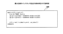
図18は、差分回路のインスタンス記述の具体例を示す説明図である。図18において、インスタンス記述1800は、差分回路がインスタンスされているコードを表している。具体的には、例えば、インスタンス記述1800には、差分回路をインスタンスしたモジュールに与えるインスタンス名が絶対パスで与えられる。
FIG. 18 is an explanatory diagram of a specific example of the instance description of the difference circuit. In FIG. 18, an
例えば、RTLのテストベンチに「diff_circuit」という名前で差分回路を置く場合、シミュレーション環境における被評価回路(対象回路)のトップのモジュールへの絶対パス(例えば、testbench.target)が指定される。この際、シミュレーション環境で階層参照可能な信号に書き換えることにより、インスタンス記述1800が作成される。
For example, when a difference circuit is placed under the name “diff_circuit” on an RTL test bench, an absolute path (for example, testbench.target) to the top module of the circuit to be evaluated (target circuit) in the simulation environment is specified. At this time, the
回路記述1700およびインスタンス記述1800によれば、差分回路の出力(例えば、out_data)に差分回路の出力信号が出力されることになる。ここで、RTLのテストベンチの記述例について説明する。なお、RTLのテストベンチは、例えば、RAM203、磁気ディスク205、光ディスク207などの記憶装置に記憶されている。
According to the
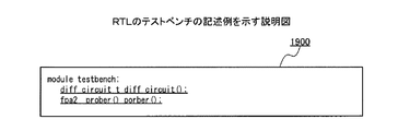
図19は、RTLのテストベンチの記述例を示す説明図である。図19において、記述1900は、RTLのテストベンチに含まれる記述であり、RTLのテストベンチ中に、後述する計測回路および差分回路をインスタンスするためのものである。図面では、RTLのテストベンチの一部を抜粋して表示している。なお、差分回路がない場合は計測回路のみに関する記述があればよい。
FIG. 19 is an explanatory diagram of a description example of an RTL test bench. In FIG. 19, a
電力見積装置200は、例えば、クロック起点データCKDおよび非クロックツリー観測ポイントデータODの中から選択されていない未選択の観測信号がなくなるまで、観測信号を選択して差分回路を作成する処理を繰り返し行う。この際、電力見積装置200は、観測信号ごとの差分回路データDFを作成してもよい。ただし、選択された観測信号の信号名に対応する信号名がRTL設計データRDに含まれる場合、差分回路データDFの作成は行われない。
For example, the
また、電力見積装置200は、クロック起点データCKDおよび非クロックツリー観測ポイントデータODの中から選択されていない未選択の観測信号がなくなるまで、図15および図16に示したような処理を行った後、差分回路データDFを作成してもよい。この場合、対象回路に対して一つの差分回路データDFが作成される。これにより、観測信号ごとの差分回路データDFを作成する場合に比べて、差分回路間の重複部分を排除することができ、差分回路の回路量を削減することができる。
In addition, the
また、電力見積装置200は、作成した差分回路データDFに対応する差分回路コンフィギュレーションデータDCGを作成する。ここで、差分回路コンフィギュレーションデータDCGは、クロックツリー観測信号/ポート番号関係表CPと、非クロックツリー観測信号/ポート番号関係表NCPと、RTL参照信号/ポート番号関係表RPとを含む。
In addition, the
ここでは、差分回路を1モジュールとし、クロックツリー観測信号/ポート番号関係表CPと、非クロックツリー観測信号/ポート番号関係表NCPとを区別しない場合を例に挙げて説明する。具体的には、クロックツリーまたは非クロックツリーのいずれかの観測信号とポート番号とが関係付けられた関係表を「観測信号/ポート番号関係表SP」とする。なお、クロックツリーの観測信号は、上述したように、部分クロックツリーに含まれる信号のうちの代表信号である。 Here, a case where the difference circuit is one module and the clock tree observation signal / port number relation table CP and the non-clock tree observation signal / port number relation table NCP are not distinguished will be described as an example. Specifically, a relation table in which observation signals of either a clock tree or a non-clock tree and port numbers are associated is referred to as an “observation signal / port number relation table SP”. Note that the observation signal of the clock tree is a representative signal among the signals included in the partial clock tree as described above.
具体的には、例えば、電力見積装置200は、RTL設計データRDの信号名が付与されている配線の端点となる入力端子と、RTL設計データRDの信号名と対応付けて表すRTL参照信号/ポート番号関係表RPを作成する。ここで、RTL参照信号/ポート番号関係表RPの具体例について説明する。
Specifically, for example, the
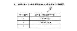
図20は、RTL参照信号/ポート番号関係表RPの具体例を示す説明図である。図20において、RTL参照信号/ポート番号関係表RPは、差分回路の入力端子のポート番号と、RTL設計データRD上の信号の信号名との関係を示す情報である。なお、RTL参照信号/ポート番号関係表RPは、図1に示した信号情報104に相当する。
FIG. 20 is an explanatory diagram showing a specific example of the RTL reference signal / port number relation table RP. In FIG. 20, the RTL reference signal / port number relationship table RP is information indicating the relationship between the port number of the input terminal of the difference circuit and the signal name of the signal on the RTL design data RD. The RTL reference signal / port number relationship table RP corresponds to the
RTL参照信号/ポート番号関係表RPによれば、差分回路の入力端子のポート番号「0」と、RTL設計データRD上の信号の信号名「TOP.A.B.C[0]」との関係を特定することができる。また、差分回路の入力端子のポート番号「1」と、RTL設計データRD上の信号の信号名「TOP.A.B.EN_A」との関係を特定することができる。 According to the RTL reference signal / port number relationship table RP, the port number “0” of the input terminal of the difference circuit and the signal name “TOP.AB.C [0]” of the signal on the RTL design data RD. Relationships can be identified. Further, the relationship between the port number “1” of the input terminal of the difference circuit and the signal name “TOP.A.B.EN_A” of the signal on the RTL design data RD can be specified.
また、電力見積装置200は、選択した観測信号と、観測信号を出力する出力端子とを対応付けて表す観測信号/ポート番号関係表SPを作成する。ここで、観測信号/ポート番号関係表SPの具体例について説明する。
In addition, the
図21は、観測信号/ポート番号関係表SPの具体例を示す説明図である。図21において、観測信号/ポート番号関係表SPは、差分回路の出力端子のポート番号と、ネットリストNL上の観測信号の信号名との関係を示す情報である。 FIG. 21 is an explanatory diagram of a specific example of the observation signal / port number relation table SP. In FIG. 21, the observation signal / port number relationship table SP is information indicating the relationship between the port number of the output terminal of the difference circuit and the signal name of the observation signal on the netlist NL.
観測信号/ポート番号関係表SPによれば、差分回路の出力端子のポート番号「0」と、観測信号の信号名「TOP.A.B.s0」との関係を特定することができる。また、差分回路の出力端子のポート番号「1」と、観測信号の信号名「TOP.A.B.s10」との関係を特定することができる。 According to the observation signal / port number relationship table SP, the relationship between the port number “0” of the output terminal of the difference circuit and the signal name “TOP.AB.s0” of the observation signal can be specified. Further, the relationship between the port number “1” of the output terminal of the difference circuit and the signal name “TOP.A.B.s10” of the observation signal can be specified.
すなわち、観測信号/ポート番号関係表SPおよびRTL参照信号/ポート番号関係表RPによれば、差分回路のどのポート番号と、どの信号がつながれるべきかを特定することができる。 That is, according to the observation signal / port number relationship table SP and the RTL reference signal / port number relationship table RP, it is possible to specify which port number of the difference circuit and which signal should be connected.
(計測回路の作成例)
つぎに、計測回路の作成例について説明する。まず、計測回路作成部304は、計測回路の計測回路計画MPを作成する。具体的には、例えば、計測回路作成部304は、計算範囲IDマップデータEDとクロック起点データCKDと非クロックツリー観測ポイントデータODとメモリ端子データMDと電力係数(ユニットセル)データPUとに基づいて、計測回路計画MPを作成する。
(Example of creating a measurement circuit)
Next, an example of creating a measurement circuit will be described. First, the measurement
図22は、計測回路計画MPの具体例を示す説明図である。図22において、計測回路計画MPは、どのような計測回路を作成するのかを決める情報である。計測回路計画MPには、例えば、コアエレメント1個当たりに接続してよい信号数の上限やコアにいれてよいコアエレメントの上限値やグルーピングの条件が記述されている。 FIG. 22 is an explanatory diagram of a specific example of the measurement circuit plan MP. In FIG. 22, the measurement circuit plan MP is information that determines what measurement circuit is to be created. In the measurement circuit plan MP, for example, an upper limit of the number of signals that can be connected per core element, an upper limit value of core elements that can be included in the core, and grouping conditions are described.
グルーピングの条件は、例えば、クロックツリーに含まれる観測信号をグルーピング対象とする条件である。また、グルーピング対象となる信号が代表信号となる部分クロックツリーが1つの計算範囲IDを持ち、全クロックツリーの電力係数の合計値に対して、その部分クロックツリーの電力係数がbound_ratio以下となる条件である。また、同一のコアに含まれるセルには宣言された順にアドレスが振られるものとし、先頭を0とする条件である。これにより、アドレスマップも同時に決めることができる。 The grouping condition is, for example, a condition in which an observation signal included in the clock tree is a grouping target. In addition, a partial clock tree in which a signal to be grouped is a representative signal has one calculation range ID, and the power coefficient of the partial clock tree is less than bound_ratio with respect to the total value of the power coefficients of all clock trees. It is. In addition, it is a condition that addresses are assigned to cells included in the same core in the order of declaration and the head is 0. As a result, the address map can be determined at the same time.
つぎに、計測回路作成部304は、計測回路の計測回路データKDを作成する。ここで、計測回路データKDのデータ構造について説明する。
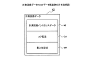
Next, the measurement
図23は、計測回路データKDのデータ構造例を示す説明図である。図23において、計測回路データKDは、計測回路インスタンスデータMIと、コア記述CAと、最上位記述MHと、を含む。最上位記述MHは、例えば、シミュレーション環境に計測回路をインスタンスするための記述である。 FIG. 23 is an explanatory diagram showing an example of the data structure of the measurement circuit data KD. In FIG. 23, the measurement circuit data KD includes measurement circuit instance data MI, a core description CA, and a top-level description MH. The top-level description MH is, for example, a description for instantiating a measurement circuit in a simulation environment.
計測回路インスタンスデータMIは、例えば、シミュレーション環境に計測回路に含まれるコアをインスタンスするための記述である。計測回路インスタンスデータMIでは、階層参照する信号の解決を行う。コア記述CAは、計測回路に含まれるコアに関する記述である。ここで、計測回路インスタンスデータMIおよび最上位記述MHの具体例について説明する。 The measurement circuit instance data MI is, for example, a description for instantiating a core included in the measurement circuit in the simulation environment. In the measurement circuit instance data MI, the signal of hierarchical reference is resolved. The core description CA is a description related to the core included in the measurement circuit. Here, specific examples of the measurement circuit instance data MI and the top-level description MH will be described.
図24は、計測回路インスタンスデータMIの具体例を示す説明図である。図24において、計測回路インスタンスデータMIには、例えば、サンプリングする区間の最大値やサンプリング期間の指定で許容すべきサイクル数が記述されている。また、計測回路計画MPで決まった計測ポイントの信号名の先頭のモジュール名をトップモジュールへのパスに置き換え、設定値にあった値を計測部品にアサインする記述が含まれている。 FIG. 24 is an explanatory diagram of a specific example of the measurement circuit instance data MI. In FIG. 24, the measurement circuit instance data MI describes, for example, the maximum value of the section to be sampled and the number of cycles that should be allowed by specifying the sampling period. Also included is a description in which the module name at the head of the signal name of the measurement point determined by the measurement circuit plan MP is replaced with a path to the top module, and a value corresponding to the set value is assigned to the measurement component.
図25は、最上位記述MHの具体例を示す説明図である。図25において、最上位記述MHは、RTLのテストベンチによってインスタンスされ、計測回路をインスタンスするための記述である。 FIG. 25 is an explanatory diagram of a specific example of the top-level description MH. In FIG. 25, a top-level description MH is a description for instantiating a measurement circuit that is instantiated by an RTL test bench.
このように、計測回路計画MPに基づいて、セルのインスタンスと階層参照との結線を行い、設定値でbundle_posedge_counter,RAM,BUS,コントローラのパラメータ値を決めている。 Thus, based on the measurement circuit plan MP, the connection between the cell instance and the hierarchy reference is performed, and the parameter values of the bundle_position_counter, RAM, BUS, and controller are determined by the set values.
また、計測回路作成部304は、差分回路が作成された場合、クロックツリー観測信号/ポート番号関係表CPと非クロックツリー観測信号/ポート番号関係表NCPとに基づいて、作成された差分回路に合わせて計測回路データKDを修正する。
In addition, when the difference circuit is created, the measurement
例えば、計測回路データKDの参照先は、電力見積用のネットリストNLの信号になっている。このため、計測回路作成部304は、例えば、「TOP.A.B.s0」を「testbench.target.A.B.s0」に変換して、計測回路データKD中の「testbench.target.A.B.s0」の記述を「testbench.diff_circuit.inst.out_data[0]」に置き換える。
For example, the reference destination of the measurement circuit data KD is a signal of the net list NL for power estimation. Therefore, for example, the measurement
同様に、計測回路作成部304は、「TOP.A.B.s10」から置換文字列である「testbench.target.A.B.s10」を得て、計測回路データKD中の「testbench.target.A.B.s10」の記述を「testbench.diff_circuit.inst.out_data[1]」に置き換える。これにより、差分回路に合わせて計測回路データKDを修正することができる。
Similarly, the measurement
最後に、計測回路作成部304は、計測回路計画MPに計測回路の情報を付加することにより、計測回路計画MPを更新する。ここで、計測回路計画MPの更新例について説明する。
Finally, the measurement
図26は、計測回路計画MPの更新例を示す説明図である。図26において、計測回路計画MPは、計測回路の情報(図26中、下線部分)が付加された更新後の計測回路計画MPである。図面では、計測回路計画MPの一部を抜粋して表示している。 FIG. 26 is an explanatory diagram of an example of updating the measurement circuit plan MP. In FIG. 26, the measurement circuit plan MP is the updated measurement circuit plan MP to which information on the measurement circuit (the underlined portion in FIG. 26) is added. In the drawing, a part of the measurement circuit plan MP is extracted and displayed.
なお、計測回路の作成については、例えば、特開2007−102337号公報を参照することができる。また、論理シミュレーションをソフトウェアシミュレータで実行する場合には、計測回路中のバスやRAMは不要である。また、計測回路作成部304は、グルーピング回路を用いることにより、計測回路の回路量を削減することにしてもよい。なお、グルーピング回路を用いた計測回路量の削減については、例えば、特開2009−053747号公報を参照することができる。ここで、計測回路の具体例について説明する。
For the creation of the measurement circuit, for example, JP-A-2007-102337 can be referred to. Further, when the logic simulation is executed by the software simulator, the bus and the RAM in the measurement circuit are not necessary. In addition, the measurement
図27および図28は、計測回路の回路構成例を示す説明図である。図27において、計測回路2701は、RTL設計データRDとネットリストNLとの差分回路が作成されなかった場合の観測信号の信号値が変化した回数を計測する回路である。被評価回路2702は、消費電力の見積もり対象となる対象回路を表している。
27 and 28 are explanatory diagrams illustrating circuit configuration examples of the measurement circuit. In FIG. 27, a
計測回路2701には、各コアを制御する共通のコントローラがあり、各コアにはデータを保持するためのRAMと、RAMにデータを書き込むためのバスが1つずつある。Counterは、0からバスに接続可能な計測数のMax値−1のアドレスとその時を送る。これにより、bundle_posedge_counterの中でバスに書き込むべきデータを保持するレジスタの値の転送が行われる。
The
なお、計測回路計画MPにおけるコア、コアエレメントは、計測回路2701中のbundle_posedge_counterにつながれる信号の集まりを指している。
The core and the core element in the measurement circuit plan MP indicate a collection of signals connected to the bundle_position_counter in the
また、図28において、計測回路2801は、RTL設計データRDとネットリストNLとの差分回路が作成された場合の観測信号の信号値が変化した回数を計測する回路である。差分回路インスタンス回路2802は、差分回路がインスタンスされた回路である。被評価回路2803は、消費電力の見積もり対象となる対象回路を表している。
In FIG. 28, a
(動的統計データERの具体例)
図29は、動的統計データERの具体例を示す説明図である。図29において、動的統計データERは、論理シミュレーションの実行結果を表す、あるコアのダンプデータである。コアエレメント(CE)の最大数を「1024」にした場合、メモリアドレスは、0x400(=1024)ずつ統計データが格納される。
(Specific examples of dynamic statistical data ER)
FIG. 29 is an explanatory diagram of a specific example of the dynamic statistical data ER. In FIG. 29, the dynamic statistical data ER is dump data of a certain core that represents the execution result of the logic simulation. When the maximum number of core elements (CE) is set to “1024”, statistical data is stored for each memory address by 0 × 400 (= 1024).
addressには、(address>>10)回目の(address&(1024−1))番目のCEの結果が格納される。また、0x0〜0x399は、CEが計算中に初期値が書き込まれるため無効データである。このようにして、任意のサンプリングの任意のCEの出力値を取り出すことができる。 In the address, the result of the (address & (1024-1)) th CE is stored (address >> 10). In addition, 0x0 to 0x399 are invalid data because the initial value is written while the CE is calculating. In this way, the output value of any CE with any sampling can be extracted.
(消費電力の見積例)
図30は、動的統計データERに基づく対象回路の消費電力の見積例を示す説明図である。電力算出部306は、電力係数(ユニットセル)データPUと、メモリ端子データMDと、電力係数(メモリ)データPMとを読み込んでコンピュータ処理可能なデータ構造に変換する。
(Estimated power consumption)
FIG. 30 is an explanatory diagram illustrating an example of estimating the power consumption of the target circuit based on the dynamic statistical data ER. The
つぎに、電力算出部306は、電力係数(ユニットセル)データPUと、メモリ端子データMDと、電力係数(メモリ)データPMとに基づいて、電力係数を縮退する。ここで、縮退とは、計測回路内の各セルの電力係数の合計値を用いて、計測回路の計測範囲に応じた電力を算出するための電力係数を求める処理である。具体的には、例えば、電力算出部306は、クロックツリー向けの電力係数、非クロックツリー向けの電力係数およびメモリ向けの電力係数を縮退する。
Next, the
つぎに、電力算出部306は、計算範囲IDマップデータEDと、計測回路計画MPと、現計算における電力係数と、動的統計データERとに基づいて、対象回路の消費電力を算出する。現計算における電力係数とは、縮退後の電力係数、例えば、クロックツリー向けの電力係数、非クロックツリー向けの電力係数およびメモリ向けの電力係数である。
Next, the
そして、電力算出部306は、電力計算結果出力I/Fを介してデータをダンプする。この際、電力算出部306は、計算範囲で排他的に集計した結果と計算範囲で積算的に集計した結果の2種類を計算範囲IDごとにファイルに落とす。これにより、計測対象の削減に合わせた電力計算が可能となるとともに計算回数を削減することができる。
Then, the
(電力見積データPEの出力例)
つぎに、図31〜図33を用いて、電力見積データPEの出力例について説明する。
(Example of output of power estimation data PE)
Next, an output example of the power estimation data PE will be described with reference to FIGS. 31 to 33.
図31は、電力見積データPEの出力例を示す説明図(その1)である。図31において、電力見積データPEは、対象回路内の各計算範囲について、各計算範囲の電力値と、各計算範囲の電力値および該計算範囲の子孫となる計算範囲の電力値を合算した合算電力値とを示す情報である。 FIG. 31 is an explanatory diagram (part 1) of an output example of the power estimation data PE. In FIG. 31, for each calculation range in the target circuit, the power estimation data PE is the sum of the power value of each calculation range, the power value of each calculation range, and the power value of the calculation range that is a descendant of the calculation range. This is information indicating the power value.
具体的には、電力見積データPEにおいてカンマで区切られた数値のうち、1番目の数値は、クロックツリーを構成する組み合わせセルやCGICなどの電力値を表している。2番目の数値は、組み合わせセルなどの非フリップフロップの電力値を表している。3番目の数値は、クロック端子にクロックツリーがつながっているフリップフロップのクロック端子成分の電力値を表している。 Specifically, the first numerical value among the numerical values separated by commas in the power estimation data PE represents a power value of a combination cell, a CGIC, or the like constituting the clock tree. The second numerical value represents the power value of a non-flip-flop such as a combination cell. The third numerical value represents the power value of the clock terminal component of the flip-flop whose clock tree is connected to the clock terminal.
4番目の数値は、クロック端子にクロックツリーがつながっているフリップフロップの非クロック端子成分の電力値を表している。5番目の数値は、クロック端子にクロックツリーがつながっていないフリップフロップの電力値を表している。6番目の数値は、RAM/ROMの電力値を表している。 The fourth numerical value represents the power value of the non-clock terminal component of the flip-flop whose clock tree is connected to the clock terminal. The fifth numerical value represents the power value of the flip-flop whose clock tree is not connected to the clock terminal. The sixth numerical value represents the power value of the RAM / ROM.
図32は、電力見積データPEの出力例を示す説明図(その2)である。図32において、波形グラフWGは、図31に示した電力見積データPEをグラフ化したものである。図32中、縦軸は電力値、横軸はサンプルIDを表している。サンプルIDは、例えば、所定間隔(例えば、10[μs])ごとの結果の識別子である。波形グラフWGは、下から上に向かって電力見積データPEの1番目〜6番目の数値が順にスタックされたグラフである。 FIG. 32 is an explanatory diagram (part 2) of an output example of the power estimation data PE. In FIG. 32, a waveform graph WG is a graph of the power estimation data PE shown in FIG. In FIG. 32, the vertical axis represents the power value, and the horizontal axis represents the sample ID. The sample ID is, for example, an identifier of a result at a predetermined interval (for example, 10 [μs]). The waveform graph WG is a graph in which the first to sixth numerical values of the power estimation data PE are stacked in order from the bottom to the top.
図33は、電力見積データPEの出力例を示す説明図(その3)である。図33において、見積結果リストLTは、ゲートレベルの消費電力を見積もる市販のツールA,B,C,Dの電力見積結果を示す表である。また、図33において、波形グラフWGは、図32に示した波形グラフWGのうち見積結果リストLTの波形データによる電力見積(9.26[μs])に近いと思われる付近を拡大したものである。 FIG. 33 is an explanatory diagram (part 3) of an output example of the power estimation data PE. In FIG. 33, an estimation result list LT is a table showing power estimation results of commercially available tools A, B, C, and D that estimate gate-level power consumption. In FIG. 33, the waveform graph WG is an enlarged view of the vicinity of the waveform graph WG shown in FIG. 32 that is considered to be close to the power estimation (9.26 [μs]) based on the waveform data of the estimation result list LT. is there.
波形グラフWGによれば、クロックツリー電力、フリップフロップ電力のクロックツリー部分電力は、他のツールの電力見積結果と比較的よくあっていることが分かる。また、RAM/ROMについては、計算を端折るため精度が落ちるような計算をしているものの他のツールと5[%]程度の誤差しかないことがわかる。また、非クロックツリー部分については、平均が、非フリップフロップが68[mW]、フリップフロップの非クロックツリー部分が23.5[mW]であり、合計92[mW]程度になり、他のツールと近い値となっている。 According to the waveform graph WG, it can be seen that the clock tree power and the clock tree partial power of the flip-flop power are relatively in good agreement with the power estimation results of other tools. It can also be seen that the RAM / ROM has an error of about 5 [%] with other tools that perform calculations that reduce the accuracy because the calculation is broken. In addition, regarding the non-clock tree part, the average is 68 [mW] for the non-flip flop and 23.5 [mW] for the non-flip flop, which is about 92 [mW] in total. It is close to the value.
(電力見積装置200の電力見積処理手順)
つぎに、電力見積装置200の電力見積処理手順について説明する。
(Power estimation processing procedure of power estimation apparatus 200)
Next, the power estimation processing procedure of the
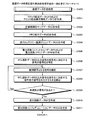
図34は、電力見積装置200の電力見積処理手順の一例を示すフローチャートである。図34のフローチャートにおいて、まず、電力見積装置200は、対象回路のRTL設計データRDおよびネットリストNLを取得したか否かを判断する(ステップS3401)。
FIG. 34 is a flowchart illustrating an example of a power estimation processing procedure of the
ここで、電力見積装置200は、RTL設計データRDおよびネットリストNLを取得するのを待つ(ステップS3401:No)。そして、電力見積装置200は、RTL設計データRDおよびネットリストNLを取得した場合(ステップS3401:Yes)、RTL設計データRDとネットリストNLとの間で同一の信号線を指す信号の対応関係を表すマッピングデータMDを作成する(ステップS3402)。
Here, the
つぎに、電力見積装置200は、マッピングデータMDと電力見積設定データSTとテクノロジーライブラリTLBとクロックソース起点データCSと配線容量データWDとに基づいて、基礎データを作成する基礎データ作成処理を実行する(ステップS3403)。基礎データ作成処理の具体的な処理手順については、図35を用いて後述する。
Next, the
そして、電力見積装置200は、計測回路計画MPに基づいて、観測信号の信号値が変化した回数を計測する計測回路を作成する(ステップS3404)。つぎに、電力見積装置200は、作成した差分回路と計測回路とをRTL用のテストベンチに実装して、RTL設計データRDに基づく対象回路の論理シミュレーションを実行する(ステップS3405)。これにより、対象回路の消費電力の見積もりに必要となる電力パラメータを抽出することができる。
Then, the
つぎに、電力見積装置200は、観測信号の信号値の変化を計測した計測結果を含む論理シミュレーションの実行結果を表す動的統計データERに基づいて、対象回路の消費電力を算出する(ステップS3406)。そして、電力見積装置200は、算出した対象回路の消費電力の算出結果を表す電力見積データPEを出力して(ステップS3407)、本フローチャートによる一連の処理を終了する。これにより、対象回路の消費電力を見積もることができる。
Next, the
つぎに、図34に示したステップS3403の基礎データ作成処理の具体的な処理手順について説明する。 Next, a specific processing procedure of the basic data creation processing in step S3403 shown in FIG. 34 will be described.
図35は、基礎データ作成処理の具体的処理手順の一例を示すフローチャートである。図35のフローチャートにおいて、まず、電力見積装置200は、ネットリストNLおよびクロックソース起点データCSに基づいてクロックツリー解析を行うことにより、クロック起点データCKDおよびクロック起点親子関係データFDを作成する(ステップS3501)。
FIG. 35 is a flowchart illustrating an example of a specific processing procedure of basic data creation processing. In the flowchart of FIG. 35, first, the
つぎに、電力見積装置200は、対象回路上の計算範囲を指定することにより、計算範囲IDマップデータEDを作成する(ステップS3502)。そして、電力見積装置200は、ネットリストNLの中からRAM/ROMを抽出することにより、メモリ端子データMDを作成する(ステップS3503)。
Next, the
つぎに、電力見積装置200は、ネットリストNLの中から非クロックツリーの信号のうちの比率rの信号をランダムに選択することにより、非クロックツリー観測ポイントデータODを作成する(ステップS3504)。そして、電力見積装置200は、対象回路内のユニットセルおよびメモリの電力係数を算出することにより、電力係数(ユニットセル)データPUおよび電力係数(メモリ)データPMを作成する(ステップS3505)。
Next, the
つぎに、電力見積装置200は、マッピングデータMDを参照して、ネットリストNL上の信号の信号名のうち、RTL設計データRD上の信号の信号名に対応する信号の信号名を特定する(ステップS3506)。そして、電力見積装置200は、クロック起点データCKDまたは非クロックツリー観測ポイントデータODの中から観測信号となる信号を選択する(ステップS3507)。
Next, the
つぎに、電力見積装置200は、ネットリストNL上の観測信号を出力するセルから後段のセルを順次辿ることにより、RTL設計データRD上の信号の信号名に対応する信号名の信号を出力するセルを検出する(ステップS3508)。そして、電力見積装置200は、クロック起点データCKDまたは非クロックツリー観測ポイントデータODの中から選択されていない未選択の信号があるか否かを判断する(ステップS3509)。
Next, the
ここで、未選択の信号がある場合(ステップS3509:Yes)、電力見積装置200は、ステップS3507に戻って、クロック起点データCKDまたは非クロックツリー観測ポイントデータODの中から観測信号となる未選択の信号を選択する(ステップS3507)。
Here, when there is an unselected signal (step S3509: Yes), the
一方、未選択の信号がない場合(ステップS3509:No)、電力見積装置200は、RTL設計データRDとネットリストNLとの差分回路を表す差分回路データDFを作成する(ステップS3510)。そして、電力見積装置200は、作成した差分回路データDFに対応する差分回路コンフィギュレーションデータDCGを作成して(ステップS3511)、図34に示したステップS3404に移行する。
On the other hand, when there is no unselected signal (step S3509: No), the
これにより、対象回路の消費電力の見積もりに必要となる電力パラメータを抽出するための差分回路を作成することができる。 Thereby, it is possible to create a differential circuit for extracting a power parameter necessary for estimating the power consumption of the target circuit.
なお、上述した説明では、クロック起点データCKDまたは非クロックツリー観測ポイントデータODの中から観測信号となる信号を選択することにしたが、これに限らない。例えば、電力見積装置200は、ユーザの操作入力により指定された信号を観測信号として選択することにしてもよい。
In the above description, the signal to be the observation signal is selected from the clock start point data CKD or the non-clock tree observation point data OD. However, the present invention is not limited to this. For example, the
以上説明したように、実施の形態にかかる電力見積装置200によれば、ネットリストNL上の観測信号を出力する第1のセルから前段のセルを順次辿ることにより、RTL設計データRDの信号と対応関係を有する信号が入力される第2のセルを検出できる。また、電力見積装置200によれば、第2のセルから第1のセルまでの部分回路をネットリストNLの中から抽出することにより、RTL設計データRDとネットリストNLとの差分回路を表す差分回路データDFを作成できる。
As described above, according to the
これにより、論理合成やレイアウト工程を経て詳細化された対象回路内のセルから出力される観測信号の波形データ、すなわち、対象回路の消費電力の見積もりに必要となる電力パラメータを抽出するための差分回路を作成することができる。 As a result, the waveform data of the observation signal output from the cells in the target circuit that have been detailed through logic synthesis and layout processes, that is, the difference for extracting the power parameters necessary for estimating the power consumption of the target circuit A circuit can be created.
また、電力見積装置200によれば、第2のセルに入力されるネットリストNLの信号と対応関係を有するRTL設計データRDの信号の信号名と、第2のセルとを対応付けて表すRTL参照信号/ポート番号関係表RPを作成することができる。これにより、差分回路の入力端子のポート番号と、RTL設計データRD上の信号の信号名との対応関係を特定することができる。
Further, according to the
また、電力見積装置200によれば、選択された観測信号の信号名と、観測信号を出力する第1のセルとを対応付けて表す観測信号/ポート番号関係表SPを作成することができる。これにより、差分回路の出力端子のポート番号と、ネットリストNL上の観測信号の信号名との対応関係を特定することができる。
Further, according to the
また、電力見積装置200によれば、ネットリストNLの中から、供給先へのクロック信号の供給を一時的に停止するセルから出力される信号を観測信号として選択することができる。これにより、論理合成時などに自動挿入されるCGICから出力される信号の波形データを抽出するための差分回路を作成することができる。
Further, according to the
また、電力見積装置200によれば、対象回路のクロックソースから辿ることができる出力端子群のうち、出力される信号の信号値が変化する単位時間当たりの回数が互いに異なる値となる出力端子から出力される信号を観測信号として選択することができる。これにより、消費電力の見積もりに必要となるトグルレートの変化点の信号の波形データを抽出するための差分回路を作成することができる。
Also, according to the
また、電力見積装置200によれば、対象回路のクロックソースから辿ることができない出力端子群のうちのいずれかの出力端子から出力される信号を観測信号として選択することができる。具体的には、例えば、電力見積装置200によれば、非クロックツリーの信号のうち比率rの信号をランダムに選択することができる。これにより、非クロックツリーの信号を間引くことができ、差分回路の回路量を抑えることができる。
Further, according to the
また、電力見積装置200によれば、RTL設計データRDと差分回路データDFと計測回路データKDとを、RTL用のテストベンチに与えて対象回路の論理シミュレーションを実行することができる。例えば、電力見積装置200は、RTL参照信号/ポート番号関係表RPと観測信号/ポート番号関係表SPとに基づいて、RTL設計データRDと差分回路データDFと計測回路データKDとをテストベンチに実装して論理シミュレーションを実行する。そして、電力見積装置200は、観測信号の信号値の変化を計測した計測結果を含む論理シミュレーションの実行結果を取得することができる。
Further, according to the
これにより、RTL設計データRDとネットリストNLとの差分回路から出力される観測信号の波形データ、すなわち、対象回路の消費電力の見積もりに必要となる電力パラメータを抽出することができる。 Thereby, the waveform data of the observation signal output from the difference circuit between the RTL design data RD and the netlist NL, that is, the power parameter necessary for estimating the power consumption of the target circuit can be extracted.
また、電力見積装置200によれば、観測信号の信号値の変化を計測した計測結果を含む論理シミュレーションの実行結果に基づいて、対象回路の消費電力を見積もることができる。これにより、従来のRTL設計データからは推測が難しかった論理合成やレイアウト工程において追加されたセルから出力される信号の波形データを用いて対象回路の消費電力の見積もることができ見積精度を向上させることができる。
Moreover, according to the
このように、電力見積装置200によれば、RTLの検証環境を使ってゲートレベルと同等の精度で消費電力を見積もることができる。また、電力見積装置200によれば、対象回路の機能検証を行うためのゲートレベルの検証環境の構築が不要となり、検証者の作業負荷を軽減することができるとともに検証期間の短縮化を図ることができる。
Thus, according to the
なお、本実施の形態で説明した電力見積支援方法は、予め用意されたプログラムをパーソナル・コンピュータやワークステーション等のコンピュータで実行することにより実現することができる。本電力見積支援方法プログラムは、ハードディスク、フレキシブルディスク、CD−ROM、MO、DVD等のコンピュータで読み取り可能な記録媒体に記録され、コンピュータによって記録媒体から読み出されることによって実行される。また、本電力見積支援方法プログラムは、インターネット等のネットワークを介して配布してもよい。 The power estimation support method described in this embodiment can be realized by executing a program prepared in advance on a computer such as a personal computer or a workstation. The power estimation support method program is recorded on a computer-readable recording medium such as a hard disk, a flexible disk, a CD-ROM, an MO, and a DVD, and is executed by being read from the recording medium by the computer. The power estimation support method program may be distributed via a network such as the Internet.
上述した実施の形態に関し、さらに以下の付記を開示する。 The following additional notes are disclosed with respect to the embodiment described above.
(付記1)コンピュータに、
消費電力の見積対象となる対象回路のネットリストの信号名とレジスタ転送レベルで記述された前記対象回路の設計情報の信号名との対応関係を表すマッピング情報を取得し、
前記ネットリストの中から信号値の変化の観測対象となる観測信号を選択し、
取得した前記マッピング情報を参照して、前記ネットリスト上の選択した前記観測信号を出力する第1のセルを起点として前段のセルを順次辿ることにより、前記設計情報の信号と対応関係を有する前記ネットリストの信号が入力される第2のセルを検出し、
検出した前記第2のセルから前記第1のセルまでの部分回路を前記ネットリストの中から抽出することにより、前記設計情報と前記ネットリストとの差分を表す差分回路情報を作成し、
前記第2のセルに入力される前記ネットリストの信号と対応関係を有する前記設計情報の信号の信号名と、前記第2のセルとを対応付けて表す信号情報を作成し、
作成した前記差分回路情報と前記信号情報とを関連付けて出力する、
処理を実行させることを特徴とする電力見積支援プログラム。
(Supplementary note 1)
Obtain mapping information indicating the correspondence between the signal name of the net list of the target circuit to be estimated for power consumption and the signal name of the design information of the target circuit described in the register transfer level,
From the netlist, select an observation signal to be observed for signal value changes,
With reference to the acquired mapping information, the first cell that outputs the selected observation signal on the netlist is sequentially traced to the preceding cell as a starting point, thereby having a correspondence with the design information signal. Detect the second cell to which the netlist signal is input,
By extracting a partial circuit from the detected second cell to the first cell from the net list, difference circuit information representing a difference between the design information and the net list is created,
Creating signal information in which the signal name of the design information signal having a correspondence relationship with the signal of the net list input to the second cell is associated with the second cell;
The generated difference circuit information and the signal information are output in association with each other.
A power estimation support program characterized by causing processing to be executed.
(付記2)前記コンピュータに、
前記観測信号の信号名と、前記観測信号を出力する前記第1のセルとを対応付けて表す観測信号情報を作成する処理を実行させ、
前記出力する処理は、
作成した前記観測信号情報と前記差分回路情報と前記信号情報とを関連付けて出力することを特徴とする付記1に記載の電力見積支援プログラム。
(Supplementary note 2)
Executing a process of creating observation signal information representing the signal name of the observation signal and the first cell that outputs the observation signal in association with each other;
The output process is as follows:
The power estimation support program according to
(付記3)前記選択する処理は、
前記ネットリストの中から、供給先へのクロック信号の供給を一時的に停止するセルから出力される信号を前記観測信号として選択することを特徴とする付記2に記載の電力見積支援プログラム。
(Supplementary note 3) The process to be selected is
The power estimation support program according to
(付記4)前記コンピュータに、
前記ネットリスト内の出力端子群の中から、前記対象回路のクロックソースから辿ることができる出力端子群を抽出する処理を実行させ、
前記選択する処理は、
抽出した前記出力端子群のうち、出力される信号の信号値が変化する単位時間当たりの回数が互いに異なる値となる出力端子から出力される信号を前記観測信号として選択することを特徴とする付記2または3に記載の電力見積支援プログラム。
(Supplementary note 4)
From the output terminal group in the netlist, to execute the process of extracting the output terminal group that can be traced from the clock source of the target circuit,
The process to select is
Note that, among the extracted output terminal groups, signals output from output terminals whose values per unit time at which the signal value of the output signal changes are different from each other are selected as the observation signals. The power estimation support program according to 2 or 3.
(付記5)前記選択する処理は、
前記ネットリスト内の出力端子群のうち、抽出した前記出力端子群を除く残余の出力端子群のいずれかの出力端子から出力される信号を前記観測信号として選択することを特徴とする付記4に記載の電力見積支援プログラム。
(Supplementary Note 5) The process to select is
(Supplementary note 4) wherein a signal output from any one of the remaining output terminal groups excluding the extracted output terminal group is selected as the observation signal among the output terminal groups in the netlist. The power estimation support program described.
(付記6)前記コンピュータに、
前記観測信号として選択した前記残余の出力端子群のいずれかの出力端子から出力される信号の信号数が閾値未満か否かを判定し、
前記信号数が前記閾値未満と判定した場合に、前記残余の出力端子群のいずれかの出力端子から出力される信号を前記観測信号として選択する、
処理を実行させることを特徴とする付記5に記載の電力見積支援プログラム。
(Appendix 6)
Determining whether the number of signals output from any output terminal of the remaining output terminal group selected as the observation signal is less than a threshold;
When the number of signals is determined to be less than the threshold, a signal output from any output terminal of the remaining output terminal group is selected as the observation signal.
The power estimation support program according to
(付記7)前記コンピュータに、
前記信号情報と前記観測信号情報とに基づいて、前記設計情報と、前記差分回路情報とを、テストベンチに与えて前記対象回路の論理シミュレーションを実行することにより、前記観測信号の信号値の変化を計測した計測結果を含む前記論理シミュレーションの実行結果を取得し、
取得した前記実行結果を出力する、
処理を実行させることを特徴とする付記2〜6のいずれか一つに記載の電力見積支援プログラム。
(Appendix 7)
Based on the signal information and the observed signal information, the design information and the difference circuit information are given to a test bench to perform a logic simulation of the target circuit, thereby changing the signal value of the observed signal. The execution result of the logic simulation including the measurement result obtained by measuring
Outputting the obtained execution result;
The power estimation support program according to any one of
(付記8)消費電力の見積対象となる対象回路のネットリストの信号名とレジスタ転送レベルで記述された前記対象回路の設計情報の信号名との対応関係を表すマッピング情報を取得する取得部と、
前記ネットリストの中から信号値の変化の観測対象となる観測信号を選択する選択部と、
前記取得部によって取得された前記マッピング情報を参照して、前記ネットリスト上の選択した前記観測信号を出力する第1のセルを起点として前段のセルを順次辿ることにより、前記設計情報の信号と対応関係を有する前記ネットリストの信号が入力される第2のセルを検出する検出部と、
前記検出部によって検出された前記第2のセルから前記第1のセルまでの部分回路を前記ネットリストの中から抽出することにより、前記設計情報と前記ネットリストとの差分を表す差分回路情報を作成する第1の作成部と、
前記第2のセルに入力される前記ネットリストの信号と対応関係を有する前記設計情報の信号の信号名と、前記第2のセルとを対応付けて表す信号情報を作成する第2の作成部と、
前記第1の作成部によって作成された前記差分回路情報と前記第2の作成部によって作成された前記信号情報とを関連付けて出力する出力部と、
を有することを特徴とする電力見積支援装置。
(Supplementary Note 8) An acquisition unit that acquires mapping information indicating a correspondence relationship between a signal name of a net list of a target circuit to be estimated for power consumption and a signal name of design information of the target circuit described in a register transfer level; ,
A selection unit for selecting an observation signal to be observed for a change in signal value from the netlist;
With reference to the mapping information acquired by the acquisition unit, by sequentially tracing the preceding cell starting from the first cell that outputs the selected observation signal on the netlist, the design information signal and A detection unit for detecting a second cell to which a signal of the netlist having a correspondence relationship is input;
By extracting a partial circuit from the second cell to the first cell detected by the detection unit from the net list, difference circuit information representing a difference between the design information and the net list is obtained. A first creation unit to be created;
A second creation unit that creates signal information in which the signal name of the design information signal having a correspondence relationship with the signal of the net list input to the second cell is associated with the second cell. When,
An output unit that associates and outputs the difference circuit information created by the first creation unit and the signal information created by the second creation unit;
A power estimation support apparatus comprising:
(付記9)コンピュータが、
消費電力の見積対象となる対象回路のネットリストの信号名とレジスタ転送レベルで記述された前記対象回路の設計情報の信号名との対応関係を表すマッピング情報を取得し、
前記ネットリストの中から信号値の変化の観測対象となる観測信号を選択し、
取得した前記マッピング情報を参照して、前記ネットリスト上の選択した前記観測信号を出力する第1のセルを起点として前段のセルを順次辿ることにより、前記設計情報の信号と対応関係を有する前記ネットリストの信号が入力される第2のセルを検出し、
検出した前記第2のセルから前記第1のセルまでの部分回路を前記ネットリストの中から抽出することにより、前記設計情報と前記ネットリストとの差分を表す差分回路情報を作成し、
前記第2のセルに入力される前記ネットリストの信号と対応関係を有する前記設計情報の信号の信号名と、前記第2のセルとを対応付けて表す信号情報を作成し、
作成した前記差分回路情報と前記信号情報とを関連付けて出力する、
処理を実行することを特徴とする電力見積支援方法。
(Supplementary note 9)
Obtain mapping information indicating the correspondence between the signal name of the net list of the target circuit to be estimated for power consumption and the signal name of the design information of the target circuit described in the register transfer level,
From the netlist, select an observation signal to be observed for signal value changes,
With reference to the acquired mapping information, the first cell that outputs the selected observation signal on the netlist is sequentially traced to the preceding cell as a starting point, thereby having a correspondence with the design information signal. Detect the second cell to which the netlist signal is input,
By extracting a partial circuit from the detected second cell to the first cell from the net list, difference circuit information representing a difference between the design information and the net list is created,
Creating signal information in which the signal name of the design information signal having a correspondence relationship with the signal of the net list input to the second cell is associated with the second cell;
The generated difference circuit information and the signal information are output in association with each other.
A power estimation support method characterized by executing processing.
100 電力見積支援装置
200 電力見積装置
301 取得部
302 マッピングデータ作成部
303 差分回路作成部
304 計測回路作成部
305 実行部
306 電力算出部
307 出力部
DESCRIPTION OF
Claims (8)
消費電力の見積対象となる対象回路のネットリストの信号名とレジスタ転送レベルで記述された前記対象回路の設計情報の信号名との対応関係を表すマッピング情報を取得し、
前記ネットリストの中から信号値の変化の観測対象となる観測信号を選択し、
取得した前記マッピング情報を参照して、前記ネットリスト上の選択した前記観測信号を出力する第1のセルを起点として前段のセルを順次辿ることにより、前記設計情報の信号と対応関係を有する前記ネットリストの信号が入力される第2のセルを検出し、
検出した前記第2のセルから前記第1のセルまでの部分回路を前記ネットリストの中から抽出することにより、前記設計情報と前記ネットリストとの差分を表す差分回路情報を作成し、
前記第2のセルに入力される前記ネットリストの信号と対応関係を有する前記設計情報の信号の信号名と、前記第2のセルとを対応付けて表す信号情報を作成し、
作成した前記差分回路情報と前記信号情報とを関連付けて出力する、
処理を実行させることを特徴とする電力見積支援プログラム。 On the computer,
Obtain mapping information indicating the correspondence between the signal name of the net list of the target circuit to be estimated for power consumption and the signal name of the design information of the target circuit described in the register transfer level,
From the netlist, select an observation signal to be observed for signal value changes,
With reference to the acquired mapping information, the first cell that outputs the selected observation signal on the netlist is sequentially traced to the preceding cell as a starting point, thereby having a correspondence with the design information signal. Detect the second cell to which the netlist signal is input,
By extracting a partial circuit from the detected second cell to the first cell from the net list, difference circuit information representing a difference between the design information and the net list is created,
Creating signal information in which the signal name of the design information signal having a correspondence relationship with the signal of the net list input to the second cell is associated with the second cell;
The generated difference circuit information and the signal information are output in association with each other.
A power estimation support program characterized by causing processing to be executed.
前記観測信号の信号名と、前記観測信号を出力する前記第1のセルとを対応付けて表す観測信号情報を作成する処理を実行させ、
前記出力する処理は、
作成した前記観測信号情報と前記差分回路情報と前記信号情報とを関連付けて出力することを特徴とする請求項1に記載の電力見積支援プログラム。 In the computer,
Executing a process of creating observation signal information representing the signal name of the observation signal and the first cell that outputs the observation signal in association with each other;
The output process is as follows:
The power estimation support program according to claim 1, wherein the generated observation signal information, the difference circuit information, and the signal information are output in association with each other.
前記ネットリストの中から、供給先へのクロック信号の供給を一時的に停止するセルから出力される信号を前記観測信号として選択することを特徴とする請求項2に記載の電力見積支援プログラム。 The process to select is
The power estimation support program according to claim 2, wherein a signal output from a cell that temporarily stops supply of a clock signal to a supply destination is selected from the netlist as the observation signal.
前記ネットリスト内の出力端子群の中から、前記対象回路のクロックソースから辿ることができる出力端子群を抽出する処理を実行させ、
前記選択する処理は、
抽出した前記出力端子群のうち、出力される信号の信号値が変化する単位時間当たりの回数が互いに異なる値となる出力端子から出力される信号を前記観測信号として選択することを特徴とする請求項2または3に記載の電力見積支援プログラム。 In the computer,
From the output terminal group in the netlist, to execute the process of extracting the output terminal group that can be traced from the clock source of the target circuit,
The process to select is
The signal output from the output terminal having a different number of times per unit time at which the signal value of the output signal changes is selected as the observation signal from the extracted output terminal group. Item 4. The power estimation support program according to Item 2 or 3.
前記ネットリスト内の出力端子群のうち、抽出した前記出力端子群を除く残余の出力端子群のいずれかの出力端子から出力される信号を前記観測信号として選択することを特徴とする請求項4に記載の電力見積支援プログラム。 The process to select is
5. The signal output from any one of the remaining output terminal groups excluding the extracted output terminal group among the output terminal groups in the netlist is selected as the observation signal. Power estimation support program described in 1.
前記信号情報と前記観測信号情報とに基づいて、前記設計情報と、前記差分回路情報とを、テストベンチに与えて前記対象回路の論理シミュレーションを実行することにより、前記観測信号の信号値の変化を計測した計測結果を含む前記論理シミュレーションの実行結果を取得し、
取得した前記実行結果を出力する、
処理を実行させることを特徴とする請求項2〜5のいずれか一つに記載の電力見積支援プログラム。 In the computer,
Based on the signal information and the observed signal information, the design information and the difference circuit information are given to a test bench to perform a logic simulation of the target circuit, thereby changing the signal value of the observed signal. The execution result of the logic simulation including the measurement result obtained by measuring
Outputting the obtained execution result;
The power estimation support program according to any one of claims 2 to 5, wherein a process is executed.
前記ネットリストの中から信号値の変化の観測対象となる観測信号を選択する選択部と、
前記取得部によって取得された前記マッピング情報を参照して、前記ネットリスト上の選択した前記観測信号を出力する第1のセルを起点として前段のセルを順次辿ることにより、前記設計情報の信号と対応関係を有する前記ネットリストの信号が入力される第2のセルを検出する検出部と、
前記検出部によって検出された前記第2のセルから前記第1のセルまでの部分回路を前記ネットリストの中から抽出することにより、前記設計情報と前記ネットリストとの差分を表す差分回路情報を作成する第1の作成部と、
前記第2のセルに入力される前記ネットリストの信号と対応関係を有する前記設計情報の信号の信号名と、前記第2のセルとを対応付けて表す信号情報を作成する第2の作成部と、
前記第1の作成部によって作成された前記差分回路情報と前記第2の作成部によって作成された前記信号情報とを関連付けて出力する出力部と、
を有することを特徴とする電力見積支援装置。 An acquisition unit for acquiring mapping information representing a correspondence relationship between a signal name of a net list of a target circuit to be estimated for power consumption and a signal name of design information of the target circuit described in a register transfer level;
A selection unit for selecting an observation signal to be observed for a change in signal value from the netlist;
With reference to the mapping information acquired by the acquisition unit, by sequentially tracing the preceding cell starting from the first cell that outputs the selected observation signal on the netlist, the design information signal and A detection unit for detecting a second cell to which a signal of the netlist having a correspondence relationship is input;
By extracting a partial circuit from the second cell to the first cell detected by the detection unit from the net list, difference circuit information representing a difference between the design information and the net list is obtained. A first creation unit to be created;
A second creation unit that creates signal information in which the signal name of the design information signal having a correspondence relationship with the signal of the net list input to the second cell is associated with the second cell. When,
An output unit that associates and outputs the difference circuit information created by the first creation unit and the signal information created by the second creation unit;
A power estimation support apparatus comprising:
消費電力の見積対象となる対象回路のネットリストの信号名とレジスタ転送レベルで記述された前記対象回路の設計情報の信号名との対応関係を表すマッピング情報を取得し、
前記ネットリストの中から信号値の変化の観測対象となる観測信号を選択し、
取得した前記マッピング情報を参照して、前記ネットリスト上の選択した前記観測信号を出力する第1のセルを起点として前段のセルを順次辿ることにより、前記設計情報の信号と対応関係を有する前記ネットリストの信号が入力される第2のセルを検出し、
検出した前記第2のセルから前記第1のセルまでの部分回路を前記ネットリストの中から抽出することにより、前記設計情報と前記ネットリストとの差分を表す差分回路情報を作成し、
前記第2のセルに入力される前記ネットリストの信号と対応関係を有する前記設計情報の信号の信号名と、前記第2のセルとを対応付けて表す信号情報を作成し、
作成した前記差分回路情報と前記信号情報とを関連付けて出力する、
処理を実行することを特徴とする電力見積支援方法。 Computer
Obtain mapping information indicating the correspondence between the signal name of the net list of the target circuit to be estimated for power consumption and the signal name of the design information of the target circuit described in the register transfer level,
From the netlist, select an observation signal to be observed for signal value changes,
With reference to the acquired mapping information, the first cell that outputs the selected observation signal on the netlist is sequentially traced to the preceding cell as a starting point, thereby having a correspondence with the design information signal. Detect the second cell to which the netlist signal is input,
By extracting a partial circuit from the detected second cell to the first cell from the net list, difference circuit information representing a difference between the design information and the net list is created,
Creating signal information in which the signal name of the design information signal having a correspondence relationship with the signal of the net list input to the second cell is associated with the second cell;
The generated difference circuit information and the signal information are output in association with each other.
A power estimation support method characterized by executing processing.
Priority Applications (1)
| Application Number | Priority Date | Filing Date | Title |
|---|---|---|---|
| JP2012154068A JP6051629B2 (en) | 2012-07-09 | 2012-07-09 | Power estimation support program, power estimation support device, and power estimation support method |
Applications Claiming Priority (1)
| Application Number | Priority Date | Filing Date | Title |
|---|---|---|---|
| JP2012154068A JP6051629B2 (en) | 2012-07-09 | 2012-07-09 | Power estimation support program, power estimation support device, and power estimation support method |
Publications (2)
| Publication Number | Publication Date |
|---|---|
| JP2014016830A true JP2014016830A (en) | 2014-01-30 |
| JP6051629B2 JP6051629B2 (en) | 2016-12-27 |
Family
ID=50111442
Family Applications (1)
| Application Number | Title | Priority Date | Filing Date |
|---|---|---|---|
| JP2012154068A Expired - Fee Related JP6051629B2 (en) | 2012-07-09 | 2012-07-09 | Power estimation support program, power estimation support device, and power estimation support method |
Country Status (1)
| Country | Link |
|---|---|
| JP (1) | JP6051629B2 (en) |
Cited By (4)
| Publication number | Priority date | Publication date | Assignee | Title |
|---|---|---|---|---|
| JP2017537374A (en) * | 2014-10-06 | 2017-12-14 | シノプシス, インコーポレイテッドSyn0Psys, Inc. | Efficient power analysis |
| CN111832737A (en) * | 2019-04-18 | 2020-10-27 | 中科寒武纪科技股份有限公司 | A data processing method and related products |
| US11847554B2 (en) | 2019-04-18 | 2023-12-19 | Cambricon Technologies Corporation Limited | Data processing method and related products |
| CN118313337A (en) * | 2024-06-11 | 2024-07-09 | 沐曦科技(成都)有限公司 | Differential circuit layout generation method and device, electronic equipment and storage medium |
Citations (4)
| Publication number | Priority date | Publication date | Assignee | Title |
|---|---|---|---|---|
| JP2008234080A (en) * | 2007-03-16 | 2008-10-02 | Ricoh Co Ltd | Semiconductor integrated circuit design support apparatus, semiconductor integrated circuit design support method, semiconductor integrated circuit design support program, semiconductor integrated circuit, and method for manufacturing semiconductor integrated circuit |
| JP2009003618A (en) * | 2007-06-20 | 2009-01-08 | Toshiba Corp | Power consumption analysis apparatus and power consumption analysis method |
| JP2009140222A (en) * | 2007-12-06 | 2009-06-25 | Fujitsu Ltd | LSI power estimation method and apparatus |
| JP2009271653A (en) * | 2008-05-02 | 2009-11-19 | Fujitsu Ltd | Power consumption estimation method, circuit design support device and program |
-
2012
- 2012-07-09 JP JP2012154068A patent/JP6051629B2/en not_active Expired - Fee Related
Patent Citations (4)
| Publication number | Priority date | Publication date | Assignee | Title |
|---|---|---|---|---|
| JP2008234080A (en) * | 2007-03-16 | 2008-10-02 | Ricoh Co Ltd | Semiconductor integrated circuit design support apparatus, semiconductor integrated circuit design support method, semiconductor integrated circuit design support program, semiconductor integrated circuit, and method for manufacturing semiconductor integrated circuit |
| JP2009003618A (en) * | 2007-06-20 | 2009-01-08 | Toshiba Corp | Power consumption analysis apparatus and power consumption analysis method |
| JP2009140222A (en) * | 2007-12-06 | 2009-06-25 | Fujitsu Ltd | LSI power estimation method and apparatus |
| JP2009271653A (en) * | 2008-05-02 | 2009-11-19 | Fujitsu Ltd | Power consumption estimation method, circuit design support device and program |
Cited By (10)
| Publication number | Priority date | Publication date | Assignee | Title |
|---|---|---|---|---|
| JP2017537374A (en) * | 2014-10-06 | 2017-12-14 | シノプシス, インコーポレイテッドSyn0Psys, Inc. | Efficient power analysis |
| US10599794B2 (en) | 2014-10-06 | 2020-03-24 | Synopsys, Inc. | Efficient power analysis |
| CN111832737A (en) * | 2019-04-18 | 2020-10-27 | 中科寒武纪科技股份有限公司 | A data processing method and related products |
| JP2021182176A (en) * | 2019-04-18 | 2021-11-25 | カンブリコン テクノロジーズ コーポレーション リミテッドCambricon Technologies Corporation Limited | Data processing methods and related products |
| JP7045357B2 (en) | 2019-04-18 | 2022-03-31 | カンブリコン テクノロジーズ コーポレーション リミテッド | Data processing methods and related products |
| US11762690B2 (en) | 2019-04-18 | 2023-09-19 | Cambricon Technologies Corporation Limited | Data processing method and related products |
| US11847554B2 (en) | 2019-04-18 | 2023-12-19 | Cambricon Technologies Corporation Limited | Data processing method and related products |
| CN111832737B (en) * | 2019-04-18 | 2024-01-09 | 中科寒武纪科技股份有限公司 | A data processing method and related products |
| US11934940B2 (en) | 2019-04-18 | 2024-03-19 | Cambricon Technologies Corporation Limited | AI processor simulation |
| CN118313337A (en) * | 2024-06-11 | 2024-07-09 | 沐曦科技(成都)有限公司 | Differential circuit layout generation method and device, electronic equipment and storage medium |
Also Published As
| Publication number | Publication date |
|---|---|
| JP6051629B2 (en) | 2016-12-27 |
Similar Documents
| Publication | Publication Date | Title |
|---|---|---|
| US6470482B1 (en) | Method and system for creating, deriving and validating structural description of electronic system from higher level, behavior-oriented description, including interactive schematic design and simulation | |
| CN115315702B (en) | Predictions based on machine learning metrics in early-stage circuit design | |
| CN103853863B (en) | Implementation method for PDK (process design kit) automatic test interface | |
| US5880971A (en) | Methodology for deriving executable low-level structural descriptions and valid physical implementations of circuits and systems from semantic specifications and descriptions thereof | |
| US5555201A (en) | Method and system for creating and validating low level description of electronic design from higher level, behavior-oriented description, including interactive system for hierarchical display of control and dataflow information | |
| US8234617B2 (en) | Method and system for re-using digital assertions in a mixed signal design | |
| US20110035203A1 (en) | system level power evaluation method | |
| US10997332B1 (en) | System and method for computing electrical over-stress of devices associated with an electronic design | |
| US6895524B2 (en) | Circuit reduction technique for improving clock net analysis performance | |
| US8938703B1 (en) | Method and apparatus for comprehension of common path pessimism during timing model extraction | |
| JP4994393B2 (en) | System and method for generating multiple models at different levels of abstraction from a single master model | |
| JP6051629B2 (en) | Power estimation support program, power estimation support device, and power estimation support method | |
| JP2012104091A (en) | Power estimation device, power estimation method and program | |
| JP2011238137A (en) | Performance estimation device | |
| US7984398B1 (en) | Automated multiple voltage/power state design process and chip description system | |
| CN120832858A (en) | Chip post-simulation verification acceleration method, system, device and storage medium | |
| US11200127B2 (en) | Automated self-check of a closed loop emulation replay | |
| JP4924130B2 (en) | Power consumption analysis support program, recording medium storing the program, and power consumption analysis support device | |
| CN118261110A (en) | Method for processing CDF parameters in PDK, method for determining difference of CDF parameters in PDK, method for iterating PDK versions, and electronic device | |
| CN101183400A (en) | Method and system for debugging and verifying graphic hardware design | |
| JP6146224B2 (en) | Determination method, determination program, and determination apparatus | |
| CN106650138A (en) | Method for automatically realizing static and dynamic temporal analysis and comparison | |
| US20210333320A1 (en) | Slew-Load Characterization | |
| US12307179B2 (en) | Detecting simulation, emulation and prototyping issues using static analysis tools | |
| CN100452062C (en) | Method for testing hardware circuit block written by hardware description language |
Legal Events
| Date | Code | Title | Description |
|---|---|---|---|
| A621 | Written request for application examination |
Free format text: JAPANESE INTERMEDIATE CODE: A621 Effective date: 20150406 |
|
| A977 | Report on retrieval |
Free format text: JAPANESE INTERMEDIATE CODE: A971007 Effective date: 20160407 |
|
| A131 | Notification of reasons for refusal |
Free format text: JAPANESE INTERMEDIATE CODE: A131 Effective date: 20160419 |
|
| A521 | Written amendment |
Free format text: JAPANESE INTERMEDIATE CODE: A523 Effective date: 20160620 |
|
| TRDD | Decision of grant or rejection written | ||
| A01 | Written decision to grant a patent or to grant a registration (utility model) |
Free format text: JAPANESE INTERMEDIATE CODE: A01 Effective date: 20161101 |
|
| A61 | First payment of annual fees (during grant procedure) |
Free format text: JAPANESE INTERMEDIATE CODE: A61 Effective date: 20161114 |
|
| R150 | Certificate of patent or registration of utility model |
Ref document number: 6051629 Country of ref document: JP Free format text: JAPANESE INTERMEDIATE CODE: R150 |
|
| LAPS | Cancellation because of no payment of annual fees |