JP2014055352A - Laser induced deposition for seed layer - Google Patents
Laser induced deposition for seed layer Download PDFInfo
- Publication number
- JP2014055352A JP2014055352A JP2013167170A JP2013167170A JP2014055352A JP 2014055352 A JP2014055352 A JP 2014055352A JP 2013167170 A JP2013167170 A JP 2013167170A JP 2013167170 A JP2013167170 A JP 2013167170A JP 2014055352 A JP2014055352 A JP 2014055352A
- Authority
- JP
- Japan
- Prior art keywords
- deposit material
- seed layer
- substrate surface
- layer
- seed
- Prior art date
- Legal status (The legal status is an assumption and is not a legal conclusion. Google has not performed a legal analysis and makes no representation as to the accuracy of the status listed.)
- Pending
Links
- 230000008021 deposition Effects 0.000 title claims abstract description 29
- 239000000463 material Substances 0.000 claims abstract description 103
- 239000000758 substrate Substances 0.000 claims abstract description 86
- 238000000034 method Methods 0.000 claims abstract description 75
- 239000002243 precursor Substances 0.000 claims abstract description 65
- 239000002245 particle Substances 0.000 claims abstract description 38
- 239000000126 substance Substances 0.000 claims abstract description 27
- 238000000151 deposition Methods 0.000 claims description 29
- 239000003054 catalyst Substances 0.000 claims description 24
- BASFCYQUMIYNBI-UHFFFAOYSA-N platinum Chemical compound [Pt] BASFCYQUMIYNBI-UHFFFAOYSA-N 0.000 claims description 22
- 229910052751 metal Inorganic materials 0.000 claims description 14
- 239000002184 metal Substances 0.000 claims description 14
- 229910052697 platinum Inorganic materials 0.000 claims description 11
- 230000003197 catalytic effect Effects 0.000 claims description 10
- 239000004065 semiconductor Substances 0.000 claims description 6
- DODHYCGLWKOXCD-UHFFFAOYSA-N C[Pt](C1(C=CC=C1)C)(C)C Chemical group C[Pt](C1(C=CC=C1)C)(C)C DODHYCGLWKOXCD-UHFFFAOYSA-N 0.000 claims description 5
- 229910052710 silicon Inorganic materials 0.000 claims description 5
- 239000010703 silicon Substances 0.000 claims description 5
- 238000010894 electron beam technology Methods 0.000 claims description 3
- 238000010884 ion-beam technique Methods 0.000 claims description 3
- 230000008569 process Effects 0.000 description 12
- 239000007789 gas Substances 0.000 description 8
- 230000008901 benefit Effects 0.000 description 6
- 238000005137 deposition process Methods 0.000 description 5
- 238000010494 dissociation reaction Methods 0.000 description 5
- 230000005593 dissociations Effects 0.000 description 5
- 238000004519 manufacturing process Methods 0.000 description 5
- 238000000231 atomic layer deposition Methods 0.000 description 4
- 238000001888 ion beam-induced deposition Methods 0.000 description 4
- OKTJSMMVPCPJKN-UHFFFAOYSA-N Carbon Chemical group [C] OKTJSMMVPCPJKN-UHFFFAOYSA-N 0.000 description 3
- XUIMIQQOPSSXEZ-UHFFFAOYSA-N Silicon Chemical compound [Si] XUIMIQQOPSSXEZ-UHFFFAOYSA-N 0.000 description 3
- 230000004913 activation Effects 0.000 description 3
- 230000004888 barrier function Effects 0.000 description 3
- 230000015572 biosynthetic process Effects 0.000 description 3
- 229910052799 carbon Inorganic materials 0.000 description 3
- 238000000313 electron-beam-induced deposition Methods 0.000 description 3
- 230000031700 light absorption Effects 0.000 description 3
- 239000000203 mixture Substances 0.000 description 3
- 238000001179 sorption measurement Methods 0.000 description 3
- 239000013077 target material Substances 0.000 description 3
- ATJFFYVFTNAWJD-UHFFFAOYSA-N Tin Chemical compound [Sn] ATJFFYVFTNAWJD-UHFFFAOYSA-N 0.000 description 2
- 239000000853 adhesive Substances 0.000 description 2
- 230000001070 adhesive effect Effects 0.000 description 2
- 239000006227 byproduct Substances 0.000 description 2
- 238000011109 contamination Methods 0.000 description 2
- 238000010438 heat treatment Methods 0.000 description 2
- 238000002347 injection Methods 0.000 description 2
- 239000007924 injection Substances 0.000 description 2
- 230000001678 irradiating effect Effects 0.000 description 2
- 230000007246 mechanism Effects 0.000 description 2
- 150000002739 metals Chemical class 0.000 description 2
- 238000012545 processing Methods 0.000 description 2
- 238000004549 pulsed laser deposition Methods 0.000 description 2
- 239000007787 solid Substances 0.000 description 2
- 229910004298 SiO 2 Inorganic materials 0.000 description 1
- 238000002679 ablation Methods 0.000 description 1
- 239000002156 adsorbate Substances 0.000 description 1
- 125000004429 atom Chemical group 0.000 description 1
- 125000004432 carbon atom Chemical group C* 0.000 description 1
- 239000007833 carbon precursor Substances 0.000 description 1
- 230000008859 change Effects 0.000 description 1
- 238000006243 chemical reaction Methods 0.000 description 1
- 229910017052 cobalt Inorganic materials 0.000 description 1
- 239000010941 cobalt Substances 0.000 description 1
- GUTLYIVDDKVIGB-UHFFFAOYSA-N cobalt atom Chemical compound [Co] GUTLYIVDDKVIGB-UHFFFAOYSA-N 0.000 description 1
- 238000010276 construction Methods 0.000 description 1
- 239000000356 contaminant Substances 0.000 description 1
- 125000004122 cyclic group Chemical group 0.000 description 1
- 230000001066 destructive effect Effects 0.000 description 1
- 238000011161 development Methods 0.000 description 1
- 230000018109 developmental process Effects 0.000 description 1
- MQIKJSYMMJWAMP-UHFFFAOYSA-N dicobalt octacarbonyl Chemical group [Co+2].[Co+2].[O+]#[C-].[O+]#[C-].[O+]#[C-].[O+]#[C-].[O+]#[C-].[O+]#[C-].[O+]#[C-].[O+]#[C-] MQIKJSYMMJWAMP-UHFFFAOYSA-N 0.000 description 1
- 239000003989 dielectric material Substances 0.000 description 1
- 230000005684 electric field Effects 0.000 description 1
- 239000012535 impurity Substances 0.000 description 1
- 238000011065 in-situ storage Methods 0.000 description 1
- 238000010849 ion bombardment Methods 0.000 description 1
- 239000003446 ligand Substances 0.000 description 1
- 238000012986 modification Methods 0.000 description 1
- 230000004048 modification Effects 0.000 description 1
- 238000012805 post-processing Methods 0.000 description 1
- 238000005086 pumping Methods 0.000 description 1
- 230000004044 response Effects 0.000 description 1
- 239000007790 solid phase Substances 0.000 description 1
- 230000002269 spontaneous effect Effects 0.000 description 1
- 238000006467 substitution reaction Methods 0.000 description 1
- 238000012546 transfer Methods 0.000 description 1
- 239000012808 vapor phase Substances 0.000 description 1
Images


Classifications
-
- C—CHEMISTRY; METALLURGY
- C23—COATING METALLIC MATERIAL; COATING MATERIAL WITH METALLIC MATERIAL; CHEMICAL SURFACE TREATMENT; DIFFUSION TREATMENT OF METALLIC MATERIAL; COATING BY VACUUM EVAPORATION, BY SPUTTERING, BY ION IMPLANTATION OR BY CHEMICAL VAPOUR DEPOSITION, IN GENERAL; INHIBITING CORROSION OF METALLIC MATERIAL OR INCRUSTATION IN GENERAL
- C23C—COATING METALLIC MATERIAL; COATING MATERIAL WITH METALLIC MATERIAL; SURFACE TREATMENT OF METALLIC MATERIAL BY DIFFUSION INTO THE SURFACE, BY CHEMICAL CONVERSION OR SUBSTITUTION; COATING BY VACUUM EVAPORATION, BY SPUTTERING, BY ION IMPLANTATION OR BY CHEMICAL VAPOUR DEPOSITION, IN GENERAL
- C23C16/00—Chemical coating by decomposition of gaseous compounds, without leaving reaction products of surface material in the coating, i.e. chemical vapour deposition [CVD] processes
- C23C16/02—Pretreatment of the material to be coated
- C23C16/0272—Deposition of sub-layers, e.g. to promote the adhesion of the main coating
- C23C16/0281—Deposition of sub-layers, e.g. to promote the adhesion of the main coating of metallic sub-layers
-
- C—CHEMISTRY; METALLURGY
- C23—COATING METALLIC MATERIAL; COATING MATERIAL WITH METALLIC MATERIAL; CHEMICAL SURFACE TREATMENT; DIFFUSION TREATMENT OF METALLIC MATERIAL; COATING BY VACUUM EVAPORATION, BY SPUTTERING, BY ION IMPLANTATION OR BY CHEMICAL VAPOUR DEPOSITION, IN GENERAL; INHIBITING CORROSION OF METALLIC MATERIAL OR INCRUSTATION IN GENERAL
- C23C—COATING METALLIC MATERIAL; COATING MATERIAL WITH METALLIC MATERIAL; SURFACE TREATMENT OF METALLIC MATERIAL BY DIFFUSION INTO THE SURFACE, BY CHEMICAL CONVERSION OR SUBSTITUTION; COATING BY VACUUM EVAPORATION, BY SPUTTERING, BY ION IMPLANTATION OR BY CHEMICAL VAPOUR DEPOSITION, IN GENERAL
- C23C16/00—Chemical coating by decomposition of gaseous compounds, without leaving reaction products of surface material in the coating, i.e. chemical vapour deposition [CVD] processes
- C23C16/04—Coating on selected surface areas, e.g. using masks
- C23C16/047—Coating on selected surface areas, e.g. using masks using irradiation by energy or particles
-
- C—CHEMISTRY; METALLURGY
- C23—COATING METALLIC MATERIAL; COATING MATERIAL WITH METALLIC MATERIAL; CHEMICAL SURFACE TREATMENT; DIFFUSION TREATMENT OF METALLIC MATERIAL; COATING BY VACUUM EVAPORATION, BY SPUTTERING, BY ION IMPLANTATION OR BY CHEMICAL VAPOUR DEPOSITION, IN GENERAL; INHIBITING CORROSION OF METALLIC MATERIAL OR INCRUSTATION IN GENERAL
- C23C—COATING METALLIC MATERIAL; COATING MATERIAL WITH METALLIC MATERIAL; SURFACE TREATMENT OF METALLIC MATERIAL BY DIFFUSION INTO THE SURFACE, BY CHEMICAL CONVERSION OR SUBSTITUTION; COATING BY VACUUM EVAPORATION, BY SPUTTERING, BY ION IMPLANTATION OR BY CHEMICAL VAPOUR DEPOSITION, IN GENERAL
- C23C16/00—Chemical coating by decomposition of gaseous compounds, without leaving reaction products of surface material in the coating, i.e. chemical vapour deposition [CVD] processes
- C23C16/06—Chemical coating by decomposition of gaseous compounds, without leaving reaction products of surface material in the coating, i.e. chemical vapour deposition [CVD] processes characterised by the deposition of metallic material
- C23C16/18—Chemical coating by decomposition of gaseous compounds, without leaving reaction products of surface material in the coating, i.e. chemical vapour deposition [CVD] processes characterised by the deposition of metallic material from metallo-organic compounds
Landscapes
- Chemical & Material Sciences (AREA)
- Metallurgy (AREA)
- Chemical Kinetics & Catalysis (AREA)
- Engineering & Computer Science (AREA)
- Materials Engineering (AREA)
- Mechanical Engineering (AREA)
- General Chemical & Material Sciences (AREA)
- Organic Chemistry (AREA)
- Health & Medical Sciences (AREA)
- Toxicology (AREA)
- Physical Vapour Deposition (AREA)
- Chemical Vapour Deposition (AREA)
- Catalysts (AREA)
- Electrodes Of Semiconductors (AREA)
Abstract
Description
本発明は、基板の表面に材料を付着させる方法に関する。 The present invention relates to a method for depositing a material on a surface of a substrate.
電子ビーム誘起付着(electron beam induced deposition)(EBID)、イオン・ビーム誘起付着(ion beam induced deposition)(IBID)などの荷電粒子ビーム誘起付着プロセスは、表面に吸着させた前駆体分子を、電子衝撃またはイオン衝撃によって解離させることを含む。一般的な実施では、高真空システム内に位置する基板の表面から数ミリメートルのところに配置された中空針によって気相前駆体を送達する。基板表面に吸着層を形成した後、吸着物で覆われた基板表面に荷電粒子ビームを照射する。基板−真空界面を横切るときに、荷電粒子は、非弾性散乱によって、そのエネルギーの一部を、基板表面に吸着させた前駆体分子に伝達する。伝達されるエネルギーが十分な場合には、分子の結合が破壊され、前駆体は、安定な固相成分と揮発性の副生物とに「解離」する。固体成分は、基板表面に接着して付着物を形成し、それによってナノメートルからマイクロメートル・サイズの特徴部分の直接書込みを可能にする。このプロセスは一般に付着と呼ばれる。この解離過程によって生成した揮発性副生物は、続いて基板から脱離し、ポンピング・システムによって除去される。 Charged particle beam induced deposition processes such as electron beam induced deposition (EBID) and ion beam induced deposition (IBID) are used to bombard precursor molecules adsorbed on the surface with electron bombardment. Or dissociation by ion bombardment is included. In a typical implementation, the vapor phase precursor is delivered by a hollow needle located a few millimeters from the surface of the substrate located in the high vacuum system. After the adsorption layer is formed on the substrate surface, the charged particle beam is irradiated onto the substrate surface covered with the adsorbate. When traversing the substrate-vacuum interface, the charged particles transfer some of their energy to the precursor molecules adsorbed on the substrate surface by inelastic scattering. If the energy transferred is sufficient, the molecular bonds are broken and the precursor “dissociates” into stable solid phase components and volatile by-products. The solid component adheres to the substrate surface to form a deposit, thereby allowing direct writing of nanometer to micrometer sized features. This process is commonly referred to as deposition. Volatile by-products generated by this dissociation process are subsequently desorbed from the substrate and removed by a pumping system.
電子ビームおよびイオン・ビームを、伝統的な光学系で達成可能なスポット・サイズよりも小さなスポット・サイズに集束させることができることはよく知られている。その結果、荷電粒子ビーム誘起付着プロセスによって形成される特徴部分を、パルス・レーザ付着(pulsed laser deposition)(PLD)、直接書込みレーザ支援付着(direct−write laser−assisted deposition)などのレーザ誘起プロセスによって形成される特徴部分よりも小さくすることができる。しかしながら、E/IBIDは比較的に低速のプロセスであるため、それらの技法を使用して付着物を厚くまたは大面積に付着させると、処理時間が長くなる。それに加えて、荷電粒子ビーム技法を用いて付着させた付着物の純度はしばしば低い。理想的な導電性を有する付着物(例えば白金)では、純度が低い(例えば炭素汚染がある)と、導電率が、理想的な導電率よりも低くなる。一般に、汚染物質が含まれると、付着させる目的の材料の所望の特性は悪化する。 It is well known that electron and ion beams can be focused to a spot size smaller than that achievable with traditional optics. As a result, the features formed by the charged particle beam induced deposition process can be transformed by laser induced processes such as pulsed laser deposition (PLD), direct write laser assisted deposition (Direct-write laser-assisted deposition). It can be made smaller than the feature formed. However, because E / IBID is a relatively slow process, using these techniques to deposit deposits thick or large areas increases processing time. In addition, the purity of deposits deposited using charged particle beam techniques is often low. For deposits having ideal conductivity (for example, platinum), the conductivity is lower than the ideal conductivity if the purity is low (for example, there is carbon contamination). In general, the inclusion of contaminants degrades the desired properties of the intended material to be deposited.
新規の処理、後処理または新規の前駆体選択によって純度および/または材料特性を向上させることを目指すビーム・ケミストリに関係した文献が存在する。そのような1つの文献は、高純度、低抵抗率のスズ材料をIBIDによって付着させる目的に使用することができる新規の前駆体、ヘキサメチル二スズを記載している。別の文献には、EBIDシードを使用して、循環的な自発反応による原子層付着を介した成長を誘導するビーム・シード(beam−seeded)原子層付着(atomic layer deposition)(ALD)技法が記載されている。この技法の結果は、触媒位置だけに局在した純粋な付着物である。しかしながら、どちらの技法にも欠点がある。スズの付着は、高度のガス閉じ込めが存在するバイアおよび表面下の特徴部分でしか達成されない傾向がある。ALDプロセスはやや低速で再現不可能であることがあり、真空汚染が問題になる。光分解機構と熱分解機構の両方を含む連続波レーザ誘起付着およびナノ秒パルス・レーザ誘起付着に関する多くの文献がある。しかしながら、これらの機構は基板を加熱する傾向があり、基板の加熱は望ましくないことがある。 There is literature related to beam chemistry that aims to improve purity and / or material properties by new processing, post-processing or selection of new precursors. One such document describes a novel precursor, hexamethyldistin, that can be used for the purpose of depositing high purity, low resistivity tin materials by IBID. Another document includes a beam-seeded atomic layer deposition (ALD) technique that uses EBID seeds to induce growth through atomic layer deposition by cyclic spontaneous reactions. Have been described. The result of this technique is a pure deposit localized only at the catalyst location. However, both techniques have drawbacks. Tin deposition tends to be achieved only in vias and subsurface features where a high degree of gas confinement exists. The ALD process is somewhat slow and not reproducible, and vacuum contamination becomes a problem. There is a lot of literature on continuous wave laser induced deposition and nanosecond pulsed laser induced deposition, including both photolytic and pyrolytic mechanisms. However, these mechanisms tend to heat the substrate, which can be undesirable.
したがって、新規の高純度付着プロセス、特に、純金属、誘電体および半導体の大面積付着と小面積付着の両方を可能にする方法が依然として求められている。 Accordingly, there remains a need for new high purity deposition processes, particularly methods that allow both large and small area deposition of pure metals, dielectrics and semiconductors.
本発明の目的は、基板の表面に、任意のパターンの材料を付着させることである。 An object of the present invention is to deposit an arbitrary pattern of material on the surface of a substrate.
独立した第1の態様では、本発明は、基板表面に目的の付着物材料の層を形成する方法である。この方法は、基板表面を真空中に置き、この基板表面を、前駆体分子を含む第1の化学蒸気にさらすことから始まり、この前駆体分子は、荷電粒子ビームを照射すると、荷電粒子を照射した領域にだけ、付着したシード層を形成する。この最初の局所的な荷電粒子誘起付着の目的は、この付着した材料が、光吸収特性を変化させ、目的の付着物材料前駆体ガスの付着係数(sticking coefficient)/滞留時間を変化させ、および/または解離に対する活性化障壁を低くすることによって、後続の目的の付着物材料の付着を促進することである。このシード層の付着の結果、続いて前駆体分子の層で覆うことができる新たな固体表面が形成される。次いで、このシード層を、(最初の前駆体と同じまたは異なる)目的の付着物材料前駆体分子を含む第2の化学蒸気にさらす。この目的の付着物材料前駆体分子はシード層の表面に吸着する。最後に、基板にレーザ・ビームを当てる。シード層とレーザ・ビームが当たったエリアとの交線および交線の周囲に、目的の付着物材料層が形成される。この目的の付着物材料層の形成は例えば、上述の活性化障壁、光吸収特性および/または蒸気吸着特性の変化によって起こる。好ましい一実施形態では、基板を荷電粒子ビームで走査して、パターン形成されたシード層を形成する。好ましい他の実施形態では、荷電粒子ビームを移動させない。 In a first independent aspect, the present invention is a method of forming a layer of a target deposit material on a substrate surface. The method begins by placing the substrate surface in a vacuum and exposing the substrate surface to a first chemical vapor containing precursor molecules that, when irradiated with a charged particle beam, irradiate charged particles. A deposited seed layer is formed only in the areas that have been exposed. The purpose of this first localized charged particle induced deposition is that the deposited material changes the light absorption properties, changes the sticking coefficient / dwell time of the target deposit material precursor gas, and To promote the subsequent deposition of the target deposit material by lowering the activation barrier against dissociation. This seed layer deposition results in the formation of a new solid surface that can subsequently be covered with a layer of precursor molecules. This seed layer is then exposed to a second chemical vapor containing the desired deposit material precursor molecules (same or different from the first precursor). The target deposit material precursor molecules adsorb on the surface of the seed layer. Finally, a laser beam is applied to the substrate. A target deposit material layer is formed at and around the intersection of the seed layer and the area hit by the laser beam. The formation of the deposit material layer for this purpose occurs, for example, by a change in the activation barrier, light absorption properties and / or vapor adsorption properties described above. In a preferred embodiment, the substrate is scanned with a charged particle beam to form a patterned seed layer. In another preferred embodiment, the charged particle beam is not moved.
独立した第2の態様では、本発明は、目的の付着物材料の層を、この目的の付着物材料のレーザ誘起付着を容易にするシード層を有する基板表面に付着させる方法の形をとる。この方法は、基板表面エリアを真空中に置き、この基板表面エリアを、その目的の付着物材料用の前駆体分子を含む化学蒸気にさらすことから始まる。次いで、このエリアにレーザ・ビームを当てる。レーザ・ビームがシード層に当たったところに目的の付着物材料層が形成される。 In a second independent aspect, the present invention takes the form of a method of depositing a layer of target deposit material on a substrate surface having a seed layer that facilitates laser-induced deposition of the target deposit material. The method begins by placing the substrate surface area in a vacuum and exposing the substrate surface area to a chemical vapor containing precursor molecules for the intended deposit material. A laser beam is then applied to this area. The target deposit material layer is formed where the laser beam strikes the seed layer.
以上では、以下の本発明の詳細な説明をより十分に理解できるように、本発明の特徴および技術上の利点をかなり広く概説した。以下では、本発明の追加の特徴および利点を説明する。開示される着想および特定の実施形態を、本発明の同じ目的を達成するために他の構造を変更しまたは設計するベースとして容易に利用することができることを当業者は理解すべきである。さらに、このような等価の構造は、添付の特許請求の範囲に記載された本発明の趣旨および範囲を逸脱しないことを当業者は理解すべきである。 The foregoing has outlined rather broadly the features and technical advantages of the present invention in order that the detailed description of the invention that follows may be better understood. The following describes additional features and advantages of the present invention. It should be understood by those of ordinary skill in the art that the disclosed concepts and specific embodiments can be readily utilized as a basis for modifying or designing other structures to accomplish the same objectives of the present invention. Moreover, those skilled in the art should appreciate that such equivalent constructions do not depart from the spirit and scope of the invention as set forth in the appended claims.
次に、本発明および本発明の利点のより完全な理解のため、添付図面に関して書かれた以下の説明を参照する。 For a more complete understanding of the present invention and its advantages, reference is now made to the following description, taken in conjunction with the accompanying drawings.
本発明の実施形態は、基板表面に材料を付着させる方法を対象とする。 Embodiments of the present invention are directed to a method of depositing material on a substrate surface.
定義:超短パルス・レーザ(ultrashort pulsed laser)は、持続時間が10ピコ秒未満の光パルスを発射するレーザである。関数的には、超短レジームには、材料応答の強度依存性が電場の2乗(またはより高次の累乗)によって支配されているときに入る。超短パルス・レーザ・ビームは、超短パルス・レーザによって発射されたビームである。 Definition: An ultrashort pulsed laser is a laser that emits light pulses having a duration of less than 10 picoseconds. Functionally, the ultrashort regime is entered when the strength dependence of the material response is dominated by the square (or higher order power) of the electric field. An ultrashort pulse laser beam is a beam emitted by an ultrashort pulse laser.
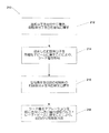
図1および5を参照すると、本発明の工程を実施する好ましい方法210(図5)を実現するための構成110は、真空中に基板112を含み、この基板112を、ガス注入源116によって蒸気114にさらす(ステップ212)。源116は一般に、基板112の表面の上方1mm未満のところに配置された針である(ただしそうでなければならないというわけではない)。蒸気114は、シード付着物材料用の前駆体分子を含み、この前駆体分子は、基板112の表面に吸着して吸着分子115の層(図3)を形成する。
With reference to FIGS. 1 and 5, a
吸着した前駆体分子115に荷電粒子ビーム118を照射すると(ステップ214)、シード付着物材料の前駆体分子115は解離し、シード付着物材料のシード層120が付着する。好ましい一実施形態では、シード層120が、白金などの触媒金属である。この場合、白金層120は不純物を含む。これは明らかに、前駆体分子の完全な解離を達成するのに荷電粒子ビームのパワー密度が不十分であり、そのため、炭素原子および/またはその他の原子が白金と一緒に付着するためである。触媒金属シード層は、目的の付着物材料の前駆体分子の解離に対する活性化障壁を低くすることにより目的の付着物材料の付着を促進する。好ましい他の実施形態では、シード付着物材料が、目的の付着物材料の付着係数/滞留時間または基板の光吸収特性を変化させる。
When the
シード層120を形成した後、荷電粒子ビーム118を停止し、シード層120を、目的の材料の前駆体分子を含む第2の蒸気122にさらす(ステップ216)。この前駆体分子も基板表面に吸着して、第2の吸着前駆体分子エリア124(図4)を形成する。同時に、エリア124を、超短パルス・レーザ126で処理する(ステップ218)。その結果、触媒シード層120とほぼ一致するが、触媒シード層120よりもわずかに広がった、目的の付着物材料の高純度付着物128が形成される。付着物128が白金である場合、付着物128の純度は、触媒シード層120の純度よりもはるかに高い。
After the
好ましい一実施形態では目的の材料が白金だが、別の材料をシード層の表面および周囲に付着させる他の好ましい実施形態も多く存在する。好ましい代替実施形態では、目的の付着物材料が炭素であり、炭素前駆体分子を使用して、シード層120の表面に炭素付着物128を付着させる。
In one preferred embodiment, the target material is platinum, but there are many other preferred embodiments in which another material is deposited on and around the seed layer. In a preferred alternative embodiment, the target deposit material is carbon, and carbon precursor molecules are used to deposit the
好ましい一実施形態では、ターゲット表面における荷電粒子ビームのスポット・サイズが10nm以上である。2次荷電粒子および1次荷電粒子が広がるため、触媒シード層120の幅は一般にこのスポット・サイズよりも大きい。触媒シード層120の線幅は100から150nmの間であることが好ましく、50から100nmの間であるとより好ましく、10から50nmの間であると最も好ましい。レーザ誘起付着物の線幅は110から160nmの間であることが好ましく、60から110nmの間であるとより好ましく、15から60nmの間であると最も好ましい。この線幅は、現在使用可能な技法の結果得られる線幅と比較して勝り、微小回路の製造において有利に使用することができる。
In a preferred embodiment, the spot size of the charged particle beam at the target surface is 10 nm or more. Due to the spread of secondary and primary charged particles, the width of the
好ましい他の方法では、より幅の広い荷電粒子ビーム118を使用することによって、またはあるエリアをビーム118で走査することによって、より幅の広い触媒シード層を形成する。このより幅の広い触媒シード層は、長方形などの閉じた幾何学的形状を有することができる。純粋な材料層を形成する他の技法も知られているが、本発明の方法の利点は、幅に関する制限がないときに、形成中に基板または層120を潜在的に破壊的な熱にさらすことなく、純粋な目的の材料の層120を形成することができることである。上記の技法は、約20°C(ほぼ室温)を含む広範囲の温度で実行することができる。
In another preferred method, a wider catalyst seed layer is formed by using a wider charged
上述のとおり、好ましい一実施形態では、レーザ・ビーム124が超短パルス・レーザ・ビームである。このビームは、フルエンス(fluence)が小さく、そのため基板のアブレーション(ablation)または加熱をあまり引き起こさないという利点を有する。しかしながら状況によっては基板の加熱が許容される。したがって、好ましい代替実施形態では、ピコ秒レーザ、ナノ秒レーザまたは連続波レーザを含む別のタイプのレーザが使用される。
As mentioned above, in a preferred embodiment, the
好ましい一実施形態では、蒸気114が、白金前駆体であるトリメチル(メチルシクロペンタジエニル)白金の分子を含む。好ましい他の実施形態では、蒸気114が、コバルト前駆体であるジコバルトオクタカルボニルの分子を含む。当業者は、触媒層に対して適当な他の前駆体ガスおよび所望の金属層に対して適当な他の前駆体ガスを容易に決定することができる。触媒層120に対して適当な前駆体ガスおよび目的の材料付着物層128に対して適当な前駆体ガスは以下の特性を有する:高い蒸気圧、荷電粒子ビームによって解離させるには十分に低いが、自発的に解離するほど低くはない付着物材料−配位子間の結合エネルギー、高い付着係数および長い滞留時間。好ましい一実施形態では、基板112がシリコン基板などの半導体基板であり、好ましい他の実施形態では、基板がSiO2などの酸化物である。一般に、広範囲の基板を使用することができる。
In one preferred embodiment, the
シード層の付着速度はビーム電流に依存するが、一般的な付着速度は0.4μm3/分である。目的の材料(例えば純金属)のレーザ誘起付着は一般に0.8から1.2μm3/分の間、より好ましくは1.0から1.5μm3/分の間の速度で起こる。レーザ誘起付着の純度は一般に40%よりも高く、60%よりも高いとより好ましく、80%よりも高いと最も好ましい。 The deposition rate of the seed layer depends on the beam current, but a typical deposition rate is 0.4 μm 3 / min. Laser induced deposition of the material of interest (eg, pure metal) generally occurs at a rate between 0.8 and 1.2 μm 3 / min, more preferably between 1.0 and 1.5 μm 3 / min. The purity of laser induced deposition is generally higher than 40%, more preferably higher than 60%, and most preferably higher than 80%.
本発明のいくつかの実施形態によれば、目的の付着物材料の層を形成する方法は、前記基板表面を真空中に置き、前記基板表面を、シード付着物材料用の前駆体分子を含む第1の化学蒸気にさらし、それにより、前記シード付着物材料用の前記前駆体分子が吸着した第1の基板表面エリアを形成するステップと、前記第1の基板表面エリアに荷電粒子ビームを当て、それにより、前記荷電粒子ビームと前記第1の基板表面との交点および交点の周囲に、シード層を形成するステップと、前記シード層を、目的の付着物材料前駆体分子を含む第2の化学蒸気にさらし、それにより、目的の付着物材料前駆体分子を、前記触媒シード層の表面および周囲に吸着させるステップと、前記シード層にレーザ・ビームを当て、それにより、前記レーザ・ビームが当たった前記触媒シード層の上および周囲に目的の付着物材料層を形成するステップとを含む。 According to some embodiments of the present invention, a method of forming a layer of a target deposit material includes placing the substrate surface in a vacuum and including the precursor molecules for seed deposit material. Exposing to a first chemical vapor, thereby forming a first substrate surface area on which the precursor molecules for the seed deposit material are adsorbed; and applying a charged particle beam to the first substrate surface area Thereby forming a seed layer at and around the intersection of the charged particle beam and the first substrate surface; and the seed layer comprising a target deposit material precursor molecule Exposure to chemical vapor, thereby adsorbing the desired deposit material precursor molecules on and around the surface of the catalyst seed layer, and applying a laser beam to the seed layer, whereby the laser On and around the catalyst seed layer over beam hits and forming a deposit material layer of interest.
いくつかの実施形態では、前記シード付着物材料が触媒金属である。いくつかの実施形態では、前記触媒金属が白金である。いくつかの実施形態では、前記前駆体分子がトリメチル(メチルシクロペンタジエニル)白金である。いくつかの実施形態では、前記目的の付着物材料が前記シード付着物材料と同じである。いくつかの実施形態では、前記第1の化学蒸気と前記第2の化学蒸気とが同じである。 In some embodiments, the seed deposit material is a catalytic metal. In some embodiments, the catalytic metal is platinum. In some embodiments, the precursor molecule is trimethyl (methylcyclopentadienyl) platinum. In some embodiments, the target deposit material is the same as the seed deposit material. In some embodiments, the first chemical vapor and the second chemical vapor are the same.
いくつかの実施形態では、前記荷電粒子ビームが電子ビームである。いくつかの実施形態では、前記荷電粒子ビームがイオン・ビームである。いくつかの実施形態では、前記レーザ・ビームが超短パルス・レーザ・ビームである。 In some embodiments, the charged particle beam is an electron beam. In some embodiments, the charged particle beam is an ion beam. In some embodiments, the laser beam is an ultrashort pulse laser beam.
いくつかの実施形態では、前記基板が半導体材料でできている。いくつかの実施形態では、前記基板がシリコンでできている。いくつかの実施形態では、前記基板が酸化物でできている。いくつかの実施形態では、前記目的の付着物材料層がパターンの特徴部分を有するパターンを形成し、100nm未満の幅を有する少なくとも1つのパターンの特徴部分を含む。いくつかの実施形態では、前記パターンが、30nm未満の幅を有する少なくとも1つのパターンの特徴部分を含む。 In some embodiments, the substrate is made of a semiconductor material. In some embodiments, the substrate is made of silicon. In some embodiments, the substrate is made of an oxide. In some embodiments, the target deposit material layer forms a pattern having pattern features and includes at least one pattern feature having a width of less than 100 nm. In some embodiments, the pattern includes at least one pattern feature having a width of less than 30 nm.
いくつかの実施形態では、前記パターンが閉じた幾何学的形状である。いくつかの実施形態では、前記閉じた幾何学的形状が長方形である。いくつかの実施形態では、前記閉じた幾何学的形状の面積が1,000平方ミクロンよりも大きい。いくつかの実施形態では、前記レーザ・ビームが超短パルス・レーザ・ビームである。 In some embodiments, the pattern is a closed geometric shape. In some embodiments, the closed geometric shape is rectangular. In some embodiments, the area of the closed geometry is greater than 1,000 square microns. In some embodiments, the laser beam is an ultrashort pulse laser beam.
いくつかの実施形態では、この方法が、前記基板表面を、別のシード付着物材料用の前駆体分子を含む別のシード層化学蒸気にさらし、それにより、前記別のシード付着物材料用の前記前駆体分子が吸着した別の基板表面エリアを形成するステップと、前記別の基板表面エリアに荷電粒子ビームを当て、それにより、前記荷電粒子ビームと前記第1の基板表面との交点および交点の周囲に、シード層を形成するステップと、前記シード層を、別の目的の付着物材料前駆体分子を含む別の目的の付着物材料化学蒸気にさらし、それにより、目的の付着物材料前駆体分子を、前記触媒シード層の表面および周囲に吸着させるステップと、前記シード層にレーザ・ビームを当て、それにより、前記レーザ・ビームが当たった前記触媒シード層の上および周囲に目的の付着物材料層を形成するステップとをさらに含む。いくつかの実施形態では、前記基板表面を別のシード層化学蒸気にさらす前記ステップ、前記別の基板表面エリアに荷電粒子ビームを当てる前記ステップ、前記シード層を別の目的の付着物材料化学蒸気にさらす前記ステップ、および前記シード層にレーザ・ビームを当てる前記ステップを、所定の特性を有する積層された付着物が形成されるまで繰り返し実行する。 In some embodiments, the method exposes the substrate surface to another seed layer chemical vapor that includes precursor molecules for another seed deposit material, thereby providing for the other seed deposit material. Forming another substrate surface area on which the precursor molecules have been adsorbed, and applying a charged particle beam to the other substrate surface area, whereby intersections and intersections of the charged particle beam and the first substrate surface Forming a seed layer around the substrate, and exposing the seed layer to another target deposit material chemical vapor comprising another target deposit material precursor molecule, thereby forming the target deposit material precursor Body molecules are adsorbed on and around the surface of the catalyst seed layer, and a laser beam is applied to the seed layer, whereby an upper surface of the catalyst seed layer hit by the laser beam is applied. Fine ambient further comprises a step of forming a deposit material layer of interest. In some embodiments, the step of exposing the substrate surface to another seed layer chemical vapor, the step of applying a charged particle beam to the other substrate surface area, the seed layer being another target deposit material chemical vapor. The step of exposing to light and the step of irradiating the seed layer with a laser beam are repeated until a stacked deposit having predetermined characteristics is formed.
本発明のいくつかの実施形態によれば、目的の付着物材料の層を、前記目的の付着物材料の付着を容易にするシード層を有する基板表面に付着させる方法は、前記基板表面を真空中に置き、前記基板表面を、前記目的の付着物材料用の前駆体分子を含む化学蒸気にさらすステップと、前記エリアにレーザ・ビームを当て、それにより、前記触媒シード層の上および周囲に目的の付着物材料層を形成するステップとを含む。 According to some embodiments of the present invention, a method of depositing a layer of target deposit material on a substrate surface having a seed layer that facilitates deposition of the target deposit material includes: vacuuming the substrate surface. Placing the substrate surface in a chemical vapor containing precursor molecules for the target deposit material, and applying a laser beam to the area, thereby over and around the catalyst seed layer Forming a target deposit material layer.
いくつかの実施形態では、前記レーザ・ビームが超短パルス・レーザ・ビームである。いくつかの実施形態では、前記シード層が触媒金属でできている。いくつかの実施形態では、前記触媒金属が白金である。いくつかの実施形態では、前記前駆体分子がトリメチル(メチルシクロペンタジエニル)白金である。 In some embodiments, the laser beam is an ultrashort pulse laser beam. In some embodiments, the seed layer is made of a catalytic metal. In some embodiments, the catalytic metal is platinum. In some embodiments, the precursor molecule is trimethyl (methylcyclopentadienyl) platinum.
いくつかの実施形態では、前記基板が半導体材料でできている。いくつかの実施形態では、前記基板がシリコンでできている。いくつかの実施形態では、前記基板が酸化物でできている。いくつかの実施形態では、前記目的の付着物材料層がパターンの特徴部分を有するパターンを形成し、100nm未満の幅を有する少なくとも1つのパターンの特徴部分を含む。いくつかの実施形態では、前記パターンが、30nm未満の幅を有するパターンの特徴部分を有する。 In some embodiments, the substrate is made of a semiconductor material. In some embodiments, the substrate is made of silicon. In some embodiments, the substrate is made of an oxide. In some embodiments, the target deposit material layer forms a pattern having pattern features and includes at least one pattern feature having a width of less than 100 nm. In some embodiments, the pattern has pattern features having a width of less than 30 nm.
いくつかの実施形態では、前記目的のパターンが閉じた幾何学的形状である。いくつかの実施形態では、前記閉じた幾何学的形状が長方形である。いくつかの実施形態では、前記閉じた幾何学的形状の面積が1,000平方ミクロンよりも大きい。 In some embodiments, the pattern of interest is a closed geometric shape. In some embodiments, the closed geometric shape is rectangular. In some embodiments, the area of the closed geometry is greater than 1,000 square microns.
いくつかの実施形態では、この方法が、前記基板表面を、別のシード付着物材料用の前駆体分子を含む別のシード層化学蒸気にさらし、それにより、前記別のシード付着物材料用の前記前駆体分子が吸着した別の基板表面エリアを形成するステップと、前記別の基板表面エリアに荷電粒子ビームを当て、それにより、前記荷電粒子ビームと前記第1の基板表面との交点および交点の周囲に、シード層を形成するステップと、前記別のシード層を、別の目的の付着物材料前駆体分子を含む別の目的の付着物材料化学蒸気にさらし、それにより、別の目的の付着物材料前駆体分子を、前記触媒シード層の表面および周囲に吸着させるステップと、前記別のシード層にレーザ・ビームを当て、それにより、前記レーザ・ビームが当たった前記触媒シード層の上および周囲に目的の付着物材料層を形成するステップとをさらに含む。いくつかの実施形態では、前記基板表面を別のシード層化学蒸気にさらす前記ステップ、前記別の基板表面エリアに荷電粒子ビームを当てる前記ステップ、前記シード層を別の目的の付着物材料化学蒸気にさらす前記ステップ、および前記シード層にレーザ・ビームを当てる前記ステップを、所定の特性を有する積層付着物が形成されるまで繰り返し実行する。 In some embodiments, the method exposes the substrate surface to another seed layer chemical vapor that includes precursor molecules for another seed deposit material, thereby providing for the other seed deposit material. Forming another substrate surface area on which the precursor molecules have been adsorbed, and applying a charged particle beam to the other substrate surface area, whereby intersections and intersections of the charged particle beam and the first substrate surface Forming a seed layer around, and subjecting said another seed layer to another target deposit material chemical vapor comprising another target deposit material precursor molecule, thereby providing another target layer Adhesive material precursor molecules are adsorbed on and around the surface of the catalyst seed layer, and a laser beam is applied to the other seed layer, thereby causing the catalyst seed to be struck by the laser beam. On and around de layer further comprises a step of forming a deposit material layer of interest. In some embodiments, the step of exposing the substrate surface to another seed layer chemical vapor, the step of applying a charged particle beam to the other substrate surface area, the seed layer being another target deposit material chemical vapor. The step of exposing to light and the step of irradiating the seed layer with a laser beam are repeatedly performed until a laminate deposit having predetermined characteristics is formed.
本発明および本発明の利点を詳細に説明したが、添付の特許請求の範囲によって定義された本発明の趣旨および範囲から逸脱することなく、本明細書に、さまざまな変更、置換および改変を加えることができることを理解すべきである。さらに、本出願の範囲が、本明細書に記載されたプロセス、機械、製造、組成物、手段、方法およびステップの特定の実施形態に限定されることは意図されていない。当業者なら本発明の開示から容易に理解するように、本明細書に記載された対応する実施形態と実質的に同じ機能を実行し、または実質的に同じ結果を達成する既存のまたは今後開発されるプロセス、機械、製造、組成物、手段、方法またはステップを、本発明に従って利用することができる。したがって、添付の特許請求の範囲は、その範囲内に、このようなプロセス、機械、製造、組成物、手段、方法またはステップを含むことが意図されている。 Having described the invention and the advantages of the invention in detail, various changes, substitutions and modifications can be made to the specification without departing from the spirit and scope of the invention as defined by the appended claims. It should be understood that it can. Furthermore, it is not intended that the scope of the application be limited to the specific embodiments of the processes, machines, manufacture, compositions, means, methods, and steps described herein. Those skilled in the art will readily understand from the present disclosure that existing or future developments that perform substantially the same function or achieve substantially the same results as the corresponding embodiments described herein. Any process, machine, manufacture, composition, means, method or step that can be utilized can be utilized in accordance with the present invention. Accordingly, the appended claims are intended to include within their scope such processes, machines, manufacture, compositions of matter, means, methods, or steps.
好ましい追加の実施形態では、上述のとおりに最初のシード層を付着させ、レーザ誘起付着プロセスを実行する。しかしながら、その後、追加のシード層を付着させ、続いて別の目的の付着物材料のレーザ付着を再び実行する。この2層付着プロセスを、所望の厚さに達するまで繰り返し実行する。このプロセスを使用して、他の方法で可能な付着物よりも所望の形状および内部構造により近い積層付着物を循環的に付着させることができる。好ましい一実施形態では、この別の目的の付着物材料層に対する前駆体分子を付着サイクルごとに変更して、交互に配置された材料スタックを形成する。この実施形態では、多数の目的の付着物材料層に対して最適化するために、荷電粒子ビーム付着シード層に対する前駆体分子も変更することができる。一例として、発光ダイオード、ダイオード・レーザ、量子井戸構造体または他の発光デバイスの製造を可能にするために、いくつかの異なる前駆体を使用して、発光材料と金属とからなるスタックをその場で形成することができる。 In a preferred additional embodiment, an initial seed layer is deposited as described above and a laser induced deposition process is performed. However, an additional seed layer is then deposited, followed by another laser deposition of another target deposit material. This bilayer deposition process is repeated until the desired thickness is reached. This process can be used to cyclically deposit laminate deposits that are closer to the desired shape and internal structure than otherwise possible deposits. In a preferred embodiment, the precursor molecules for this other target deposit material layer are changed from deposition cycle to deposition cycle to form an alternating material stack. In this embodiment, the precursor molecules for the charged particle beam deposition seed layer can also be modified to optimize for multiple target deposit material layers. As an example, a stack of luminescent materials and metals is used in situ using several different precursors to enable the manufacture of light emitting diodes, diode lasers, quantum well structures or other light emitting devices. Can be formed.
以下の表は、上で説明した方法で使用することができる前駆体分子の一覧である。この表は、包括的なリストではなく、単に例を示したものである。 The following table is a list of precursor molecules that can be used in the method described above. This table is not an exhaustive list but merely an example.

112 基板
114 蒸気
116 ガス注入源
118 荷電粒子ビーム
120 シード付着物材料のシード層
112
Claims (34)
基板表面を真空中に置き、前記基板表面を、シード付着物材料用の前駆体分子を含む第1の化学蒸気にさらし、それにより、前記シード付着物材料用の前記前駆体分子が吸着した第1の基板表面エリアを形成するステップと、
前記第1の基板表面エリアに荷電粒子ビームを当て、それにより、前記荷電粒子ビームと前記第1の基板表面エリアとの交点および交点の周囲に、シード層を形成するステップと、
前記シード層を、目的の付着物材料前駆体分子を含む第2の化学蒸気にさらし、それにより、目的の付着物材料前駆体分子を、前記触媒シード層の表面および周囲に吸着させるステップと、
前記シード層にレーザ・ビームを当て、それにより、前記レーザ・ビームが当たった前記触媒シード層の上および周囲に目的の付着物材料層を形成するステップと
を含む方法。 A method for forming a layer of a target deposit material comprising:
A substrate surface is placed in a vacuum, and the substrate surface is exposed to a first chemical vapor that includes precursor molecules for seed deposit material, thereby adsorbing the precursor molecules for the seed deposit material. Forming a substrate surface area of 1;
Applying a charged particle beam to the first substrate surface area, thereby forming a seed layer at and around the intersection of the charged particle beam and the first substrate surface area;
Exposing the seed layer to a second chemical vapor comprising a target deposit material precursor molecule, thereby adsorbing the target deposit material precursor molecule on and around the catalyst seed layer;
Applying a laser beam to the seed layer, thereby forming a target deposit material layer on and around the catalyst seed layer struck by the laser beam.
(b)前記別の基板表面エリアに荷電粒子ビームを当て、それにより、前記荷電粒子ビームと前記第1の基板表面との交点および交点の周囲に、シード層を形成するステップと、
(c)前記シード層を、別の目的の付着物材料前駆体分子を含む別の目的の付着物材料化学蒸気にさらし、それにより、目的の付着物材料前駆体分子を、前記触媒シード層の表面および周囲に吸着させるステップと、
(d)前記シード層にレーザ・ビームを当て、それにより、前記レーザ・ビームが当たった前記触媒シード層の上および周囲に目的の付着物材料層を形成するステップと
をさらに含む、請求項1から17のいずれか一項に記載の方法。 (A) subjecting the substrate surface to another seed layer chemical vapor containing precursor molecules for another seed deposit material, thereby adsorbing the precursor molecules for the other seed deposit material; Forming a substrate surface area of
(B) applying a charged particle beam to said another substrate surface area, thereby forming a seed layer at and around the intersection of said charged particle beam and said first substrate surface;
(C) subjecting the seed layer to another target deposit material chemical vapor comprising another target deposit material precursor molecule, whereby the target deposit material precursor molecule is exposed to the catalyst seed layer; Adsorbing to the surface and surroundings;
And (d) applying a laser beam to the seed layer, thereby forming a target deposit material layer on and around the catalyst seed layer struck by the laser beam. 18. The method according to any one of 1 to 17.
前記基板表面を真空中に置き、前記基板表面を、前記目的の付着物材料用の前駆体分子を含む化学蒸気にさらすステップと、
前記エリアにレーザ・ビームを当て、それにより、前記触媒シード層の上および周囲に目的の付着物材料層を形成するステップと
を含む方法。 A method of depositing a layer of target deposit material on a substrate surface having a seed layer that facilitates deposition of the target deposit material,
Placing the substrate surface in a vacuum and exposing the substrate surface to chemical vapor comprising precursor molecules for the target deposit material;
Applying a laser beam to the area, thereby forming a target deposit material layer on and around the catalyst seed layer.
(b)前記別の基板表面エリアに荷電粒子ビームを当て、それにより、前記荷電粒子ビームと前記第1の基板表面との交点および交点の周囲に、シード層を形成するステップと、
(c)前記シード層を、別の目的の付着物材料前駆体分子を含む別の目的の付着物材料化学蒸気にさらし、それにより、目的の付着物材料前駆体分子を、前記触媒シード層の表面および周囲に吸着させるステップと、
(d)前記シード層にレーザ・ビームを当て、それにより、前記レーザ・ビームが当たった前記触媒シード層の上および周囲に目的の付着物材料層を形成するステップと
をさらに含む、請求項1から32のいずれか一項に記載の方法。 (A) subjecting the substrate surface to another seed layer chemical vapor containing precursor molecules for another seed deposit material, thereby adsorbing the precursor molecules for the other seed deposit material; Forming a substrate surface area of
(B) applying a charged particle beam to said another substrate surface area, thereby forming a seed layer at and around the intersection of said charged particle beam and said first substrate surface;
(C) subjecting the seed layer to another target deposit material chemical vapor comprising another target deposit material precursor molecule, whereby the target deposit material precursor molecule is exposed to the catalyst seed layer; Adsorbing to the surface and surroundings;
And (d) applying a laser beam to the seed layer, thereby forming a target deposit material layer on and around the catalyst seed layer struck by the laser beam. 33. A method according to any one of.
Applications Claiming Priority (2)
| Application Number | Priority Date | Filing Date | Title |
|---|---|---|---|
| US13/600,735 US10023955B2 (en) | 2012-08-31 | 2012-08-31 | Seed layer laser-induced deposition |
| US13/600,735 | 2012-08-31 |
Publications (1)
| Publication Number | Publication Date |
|---|---|
| JP2014055352A true JP2014055352A (en) | 2014-03-27 |
Family
ID=49117659
Family Applications (1)
| Application Number | Title | Priority Date | Filing Date |
|---|---|---|---|
| JP2013167170A Pending JP2014055352A (en) | 2012-08-31 | 2013-08-09 | Laser induced deposition for seed layer |
Country Status (4)
| Country | Link |
|---|---|
| US (2) | US10023955B2 (en) |
| EP (1) | EP2703520A1 (en) |
| JP (1) | JP2014055352A (en) |
| CN (1) | CN103668109B (en) |
Families Citing this family (9)
| Publication number | Priority date | Publication date | Assignee | Title |
|---|---|---|---|---|
| US20150225845A1 (en) * | 2014-02-12 | 2015-08-13 | Electronics And Telecommunications Research Institute | Method for forming metal oxide thin film and device for printing metal oxide thin film |
| US10538844B2 (en) | 2015-09-11 | 2020-01-21 | Fei Company | Nanofabrication using a new class of electron beam induced surface processing techniques |
| JP2019514207A (en) * | 2016-03-31 | 2019-05-30 | エレクトロ サイエンティフィック インダストリーズ インコーポレーテッド | Laser seeding for conductive plating |
| US10501851B2 (en) | 2016-05-12 | 2019-12-10 | Fei Company | Attachment of nano-objects to beam-deposited structures |
| US10544039B2 (en) * | 2017-09-08 | 2020-01-28 | Texas Instruments Incorporated | Methods for depositing a measured amount of a species in a sealed cavity |
| US11355330B2 (en) * | 2017-11-14 | 2022-06-07 | Max-Planck-Gesellschaft Zur Förderung Der Wissenschaf 1 En E.V. | Uses of isobaric tags in mass spectrometry |
| CN112146967A (en) * | 2019-06-28 | 2020-12-29 | Fei 公司 | System and method for preparing and delivering biological samples for charged particle analysis |
| CA3150485A1 (en) * | 2019-08-09 | 2021-12-18 | William Marsh Rice University | Laser-induced graphene filters and methods of making and using same |
| JP7345787B2 (en) * | 2020-04-30 | 2023-09-19 | 東京エレクトロン株式会社 | Selective film formation method |
Family Cites Families (18)
| Publication number | Priority date | Publication date | Assignee | Title |
|---|---|---|---|---|
| US5104684A (en) * | 1990-05-25 | 1992-04-14 | Massachusetts Institute Of Technology | Ion beam induced deposition of metals |
| US5174826A (en) | 1991-12-06 | 1992-12-29 | General Electric Company | Laser-assisted chemical vapor deposition |
| JP4031704B2 (en) * | 2002-12-18 | 2008-01-09 | 東京エレクトロン株式会社 | Deposition method |
| US7504136B2 (en) * | 2003-12-15 | 2009-03-17 | California Institute Of Technology | Method and system for forming a film of material using plasmon assisted chemical reactions |
| US20090110848A1 (en) | 2007-10-25 | 2009-04-30 | Los Alamos National Security, Llc | Method and apparatus for high-pressure atomic-beam laser induced deposition/etching |
| US20090246413A1 (en) | 2008-03-27 | 2009-10-01 | Imra America, Inc. | Method for fabricating thin films |
| EP2313230A4 (en) | 2008-07-09 | 2017-03-08 | FEI Company | Method and apparatus for laser machining |
| EP2199434A1 (en) | 2008-12-19 | 2010-06-23 | FEI Company | Method for forming microscopic structures on a substrate |
| US8778804B2 (en) | 2009-01-30 | 2014-07-15 | Fei Company | High selectivity, low damage electron-beam delineation etch |
| EP2239628A1 (en) * | 2009-04-02 | 2010-10-13 | Fei Company | Method for forming microscopic 3D structures |
| EP2261395A1 (en) * | 2009-06-12 | 2010-12-15 | Fei Company | Au-containing layer obtainable by charged particle beam processing |
| US8524139B2 (en) | 2009-08-10 | 2013-09-03 | FEI Compay | Gas-assisted laser ablation |
| US8617668B2 (en) | 2009-09-23 | 2013-12-31 | Fei Company | Method of using nitrogen based compounds to reduce contamination in beam-induced thin film deposition |
| EP2402475A1 (en) | 2010-06-30 | 2012-01-04 | Fei Company | Beam-induced deposition at cryogenic temperatures |
| US20120207944A1 (en) * | 2010-08-17 | 2012-08-16 | Dudley Sean Finch | Fabrication and selective patterning of thin films using ion beam-enhanced atomic and molecular layer deposition |
| US8853078B2 (en) | 2011-01-30 | 2014-10-07 | Fei Company | Method of depositing material |
| US9090973B2 (en) | 2011-01-31 | 2015-07-28 | Fei Company | Beam-induced deposition of low-resistivity material |
| US9443697B2 (en) | 2012-01-31 | 2016-09-13 | Fei Company | Low energy ion beam etch |
-
2012
- 2012-08-31 US US13/600,735 patent/US10023955B2/en active Active
-
2013
- 2013-08-09 JP JP2013167170A patent/JP2014055352A/en active Pending
- 2013-08-29 EP EP13182113.4A patent/EP2703520A1/en not_active Withdrawn
- 2013-08-30 CN CN201310385527.6A patent/CN103668109B/en active Active
-
2018
- 2018-06-20 US US16/013,347 patent/US20180298490A1/en not_active Abandoned
Also Published As
| Publication number | Publication date |
|---|---|
| US10023955B2 (en) | 2018-07-17 |
| CN103668109B (en) | 2018-06-12 |
| US20180298490A1 (en) | 2018-10-18 |
| US20140065319A1 (en) | 2014-03-06 |
| EP2703520A1 (en) | 2014-03-05 |
| CN103668109A (en) | 2014-03-26 |
Similar Documents
| Publication | Publication Date | Title |
|---|---|---|
| US20180298490A1 (en) | Seed layer laser-induced deposition | |
| US7452477B2 (en) | Procedure for etching of materials at the surface with focussed electron beam induced chemical reaction at said surface | |
| Botman et al. | Creating pure nanostructures from electron-beam-induced deposition using purification techniques: a technology perspective | |
| JP4481592B2 (en) | Method of etching material surface using chemical reaction induced by focused electron beam | |
| Utke et al. | Gas-assisted focused electron beam and ion beam processing and fabrication | |
| JP4528302B2 (en) | How to classify carbon nanotubes | |
| JP4534215B2 (en) | Carbon nanotube growth substrate | |
| JP6440850B2 (en) | Graphene manufacturing method, graphene manufacturing apparatus, and electronic device manufacturing method | |
| JPH02504444A (en) | Selected Area Nuclei and Growth Method for Metal Chemical Deposition Using Focused Ion Beams | |
| TW202104637A (en) | Method and apparatus for forming a patterned layer of material | |
| TW200847422A (en) | Method of cleaning a patterning device, method of depositing a layer system on a substrate, system for cleaning a patterning device, and coating system for depositing a layer system on a substrate | |
| JP2007503009A (en) | Method for processing thin layers with high resolution using electron beams | |
| CN103492107A (en) | Method for preparing metal particles | |
| Perez-Roldan et al. | Oxygen-assisted purification of platinum structures deposited by ion and electron beam induced processes | |
| Han et al. | Electron-and photon-stimulated modification of GaAs (110), Si (100), and Si (111) | |
| CN109862684B (en) | Single-size strong-current cluster pulse beam generation method | |
| Gavagnin et al. | Focused Electron Beam‐Induced CVD of Iron: a Practical Guide for Direct Writing | |
| Schirmer et al. | Electron-beam-induced deposition and post-treatment processes to locally generate clean titanium oxide nanostructures on Si (100) | |
| JP2004263245A (en) | Reaction method and reactor | |
| JP2019102483A (en) | Etching method and etching apparatus | |
| KR101322799B1 (en) | Deposition apparatus and deposition method using electron beam | |
| JP5163046B2 (en) | Radiator with bonding film, bonding method between adherend and radiator, and display device | |
| US20250299936A1 (en) | Remote plasma ultraviolet enhanced deposition | |
| JP2005105381A (en) | Electron beam application equipment | |
| TWI433611B (en) | A plasma source, an ion manufacturing method, a plasma manufacturing method, and a method of manufacturing the inner package carbon cluster |