JP2014106529A - データビット深度検出方法と表示装置 - Google Patents
データビット深度検出方法と表示装置 Download PDFInfo
- Publication number
- JP2014106529A JP2014106529A JP2013169383A JP2013169383A JP2014106529A JP 2014106529 A JP2014106529 A JP 2014106529A JP 2013169383 A JP2013169383 A JP 2013169383A JP 2013169383 A JP2013169383 A JP 2013169383A JP 2014106529 A JP2014106529 A JP 2014106529A
- Authority
- JP
- Japan
- Prior art keywords
- data
- interface
- receiving end
- training pattern
- pattern signal
- Prior art date
- Legal status (The legal status is an assumption and is not a legal conclusion. Google has not performed a legal analysis and makes no representation as to the accuracy of the status listed.)
- Granted
Links
Images


Classifications
-
- G—PHYSICS
- G09—EDUCATION; CRYPTOGRAPHY; DISPLAY; ADVERTISING; SEALS
- G09G—ARRANGEMENTS OR CIRCUITS FOR CONTROL OF INDICATING DEVICES USING STATIC MEANS TO PRESENT VARIABLE INFORMATION
- G09G5/00—Control arrangements or circuits for visual indicators common to cathode-ray tube indicators and other visual indicators
-
- G—PHYSICS
- G09—EDUCATION; CRYPTOGRAPHY; DISPLAY; ADVERTISING; SEALS
- G09G—ARRANGEMENTS OR CIRCUITS FOR CONTROL OF INDICATING DEVICES USING STATIC MEANS TO PRESENT VARIABLE INFORMATION
- G09G3/00—Control arrangements or circuits, of interest only in connection with visual indicators other than cathode-ray tubes
- G09G3/20—Control arrangements or circuits, of interest only in connection with visual indicators other than cathode-ray tubes for presentation of an assembly of a number of characters, e.g. a page, by composing the assembly by combination of individual elements arranged in a matrix no fixed position being assigned to or needed to be assigned to the individual characters or partial characters
- G09G3/2092—Details of a display terminals using a flat panel, the details relating to the control arrangement of the display terminal and to the interfaces thereto
- G09G3/2096—Details of the interface to the display terminal specific for a flat panel
-
- G—PHYSICS
- G09—EDUCATION; CRYPTOGRAPHY; DISPLAY; ADVERTISING; SEALS
- G09G—ARRANGEMENTS OR CIRCUITS FOR CONTROL OF INDICATING DEVICES USING STATIC MEANS TO PRESENT VARIABLE INFORMATION
- G09G3/00—Control arrangements or circuits, of interest only in connection with visual indicators other than cathode-ray tubes
- G09G3/20—Control arrangements or circuits, of interest only in connection with visual indicators other than cathode-ray tubes for presentation of an assembly of a number of characters, e.g. a page, by composing the assembly by combination of individual elements arranged in a matrix no fixed position being assigned to or needed to be assigned to the individual characters or partial characters
- G09G3/34—Control arrangements or circuits, of interest only in connection with visual indicators other than cathode-ray tubes for presentation of an assembly of a number of characters, e.g. a page, by composing the assembly by combination of individual elements arranged in a matrix no fixed position being assigned to or needed to be assigned to the individual characters or partial characters by control of light from an independent source
- G09G3/36—Control arrangements or circuits, of interest only in connection with visual indicators other than cathode-ray tubes for presentation of an assembly of a number of characters, e.g. a page, by composing the assembly by combination of individual elements arranged in a matrix no fixed position being assigned to or needed to be assigned to the individual characters or partial characters by control of light from an independent source using liquid crystals
-
- G—PHYSICS
- G09—EDUCATION; CRYPTOGRAPHY; DISPLAY; ADVERTISING; SEALS
- G09G—ARRANGEMENTS OR CIRCUITS FOR CONTROL OF INDICATING DEVICES USING STATIC MEANS TO PRESENT VARIABLE INFORMATION
- G09G5/00—Control arrangements or circuits for visual indicators common to cathode-ray tube indicators and other visual indicators
- G09G5/003—Details of a display terminal, the details relating to the control arrangement of the display terminal and to the interfaces thereto
- G09G5/006—Details of the interface to the display terminal
-
- G—PHYSICS
- G09—EDUCATION; CRYPTOGRAPHY; DISPLAY; ADVERTISING; SEALS
- G09G—ARRANGEMENTS OR CIRCUITS FOR CONTROL OF INDICATING DEVICES USING STATIC MEANS TO PRESENT VARIABLE INFORMATION
- G09G5/00—Control arrangements or circuits for visual indicators common to cathode-ray tube indicators and other visual indicators
- G09G5/003—Details of a display terminal, the details relating to the control arrangement of the display terminal and to the interfaces thereto
- G09G5/006—Details of the interface to the display terminal
- G09G5/008—Clock recovery
-
- G—PHYSICS
- G09—EDUCATION; CRYPTOGRAPHY; DISPLAY; ADVERTISING; SEALS
- G09G—ARRANGEMENTS OR CIRCUITS FOR CONTROL OF INDICATING DEVICES USING STATIC MEANS TO PRESENT VARIABLE INFORMATION
- G09G2320/00—Control of display operating conditions
- G09G2320/06—Adjustment of display parameters
- G09G2320/0693—Calibration of display systems
-
- G—PHYSICS
- G09—EDUCATION; CRYPTOGRAPHY; DISPLAY; ADVERTISING; SEALS
- G09G—ARRANGEMENTS OR CIRCUITS FOR CONTROL OF INDICATING DEVICES USING STATIC MEANS TO PRESENT VARIABLE INFORMATION
- G09G2340/00—Aspects of display data processing
- G09G2340/04—Changes in size, position or resolution of an image
- G09G2340/0407—Resolution change, inclusive of the use of different resolutions for different screen areas
- G09G2340/0428—Gradation resolution change
-
- G—PHYSICS
- G09—EDUCATION; CRYPTOGRAPHY; DISPLAY; ADVERTISING; SEALS
- G09G—ARRANGEMENTS OR CIRCUITS FOR CONTROL OF INDICATING DEVICES USING STATIC MEANS TO PRESENT VARIABLE INFORMATION
- G09G2370/00—Aspects of data communication
- G09G2370/14—Use of low voltage differential signaling [LVDS] for display data communication
Landscapes
- Engineering & Computer Science (AREA)
- Physics & Mathematics (AREA)
- Computer Hardware Design (AREA)
- General Physics & Mathematics (AREA)
- Theoretical Computer Science (AREA)
- Crystallography & Structural Chemistry (AREA)
- Chemical & Material Sciences (AREA)
- Control Of Indicators Other Than Cathode Ray Tubes (AREA)
- Digital Computer Display Output (AREA)
- Information Transfer Systems (AREA)
- Controls And Circuits For Display Device (AREA)
- Liquid Crystal Display Device Control (AREA)
- Transforming Electric Information Into Light Information (AREA)
- Control Of El Displays (AREA)
- Synchronisation In Digital Transmission Systems (AREA)
Abstract
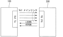
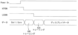
【解決手段】ホストシステムに内蔵されたインタフェース送信端と、タイミングコントローラに内蔵されたインタフェース受信端とを含み、前記インタフェース送信端は、前記送信端と受信端との間の物理的な接続が確認された後、CDR(Clock Data Recovery)トレーニングパターン信号、アライメントトレーニングパターン信号、及び表示データの順に入力データを前記インタフェース受信端に伝送し、前記インタフェース受信端は、前記CDRトレーニングパターン信号が入力される内蔵CDR回路を用いてクロックを発生し、前記アライメントトレーニングパターン信号に含まれるピクセルデータのビットまたは前記クロックをカウントし、その結果に基づいて入力データのデータビット深度を判断する。
【選択図】図4
Description
Claims (7)
- インタフェース送信端とインタフェース受信端との間の物理的な接続が確認された後、前記インタフェース送信端からCDR(Clock Data Recovery)トレーニングパターン信号が前記インタフェース受信端に伝送される段階と、
前記CDRトレーニングパターン信号を用いて前記インタフェース受信端のCDR回路からクロックが出力される段階と、
前記CDRトレーニングパターン信号に続いて、前記インタフェース送信端からアライメントトレーニングパターン信号が、前記受信端に受信される段階と、
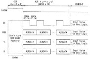
前記インタフェース受信端で前記アライメントトレーニングパターン信号に含まれるピクセルデータのビットまたは前記クロックをカウントし、その結果に基づいて入力データのデータビット深度を判断する段階と
を含むことを特徴とするデータビット深度検出方法。 - 前記インタフェース受信端で前記アライメントトレーニングパターン信号からデータイネーブル信号を分離する段階をさらに含み、
前記インタフェース受信端は、前記データイネーブル信号のハイ区間またはロー区間内で前記カウント結果として得られた累積カウント値に基づいて、前記データビット深度を判断することを特徴とする、請求項1記載のデータビット深度検出方法。 - 表示パネルと、データ駆動回路と、スキャン駆動回路と、タイミングコントローラとを含む表示装置において、
ホストシステムに内蔵されたインタフェース送信端と、
前記タイミングコントローラに内蔵されたインタフェース受信端とを含み、
前記インタフェース送信端は、前記送信端と前記受信端との間の物理的な接続が確認された後、CDR(Clock Data Recovery)トレーニングパターン信号、アライメントトレーニングパターン信号、及び表示データの順に入力データを前記インタフェース受信端に伝送し、
前記インタフェース受信端は、
前記CDRトレーニングパターン信号が入力される内蔵CDR回路を用いてクロックを発生し、前記アライメントトレーニングパターン信号に含まれるピクセルデータのビットまたは前記クロックをカウントし、その結果に基づいて入力データのデータビット深度を判断することを特徴とする表示装置。 - 前記インタフェース受信端は、
前記アライメントトレーニングパターン信号からデータイネーブル信号を分離し、
前記データイネーブル信号のハイ区間またはロー区間内で前記のカウント結果として得られた累積カウント値に基づいて、前記データビット深度を判断することを特徴とする、請求項3記載の表示装置。 - 前記インタフェース受信端は、前記データイネーブル信号のハイ区間またはロー区間内で累積カウント値が900〜1050の場合、3バイトモードと判断する一方、1200〜1400の場合、4バイトであると判断することを特徴とする、請求項4記載の表示装置。
- 前記インタフェース受信端は、所定の基準値と前記累積カウント値とを比較し、その結果に基づいて前記データビット深度を判断することを特徴とする、請求項4記載の表示装置。
- 前記インタフェース受信端は、前記データイネーブル信号のハイ区間またはロー区間内で前記の累積カウント値が1100以下の場合、3バイトモードと判断する一方、1100より大きい場合は4バイトであると判断することを特徴とする、請求項5記載の表示装置。
Applications Claiming Priority (2)
| Application Number | Priority Date | Filing Date | Title |
|---|---|---|---|
| KR1020120136118A KR102011953B1 (ko) | 2012-11-28 | 2012-11-28 | 데이터 비트 뎁쓰 검출 방법과 이를 이용한 표시장치의 인터페이스 장치 |
| KR10-2012-0136118 | 2012-11-28 |
Publications (2)
| Publication Number | Publication Date |
|---|---|
| JP2014106529A true JP2014106529A (ja) | 2014-06-09 |
| JP5763724B2 JP5763724B2 (ja) | 2015-08-12 |
Family
ID=50679128
Family Applications (1)
| Application Number | Title | Priority Date | Filing Date |
|---|---|---|---|
| JP2013169383A Active JP5763724B2 (ja) | 2012-11-28 | 2013-08-19 | データビット深度検出方法と表示装置 |
Country Status (5)
| Country | Link |
|---|---|
| US (1) | US9361825B2 (ja) |
| JP (1) | JP5763724B2 (ja) |
| KR (1) | KR102011953B1 (ja) |
| CN (1) | CN103854617B (ja) |
| DE (1) | DE102013105559B4 (ja) |
Cited By (2)
| Publication number | Priority date | Publication date | Assignee | Title |
|---|---|---|---|---|
| JP2016180853A (ja) * | 2015-03-24 | 2016-10-13 | 株式会社メガチップス | 受信装置及び画像伝送システム |
| JP2019216888A (ja) * | 2018-06-19 | 2019-12-26 | 株式会社三共 | 遊技機 |
Families Citing this family (15)
| Publication number | Priority date | Publication date | Assignee | Title |
|---|---|---|---|---|
| US6455820B2 (en) | 1999-07-27 | 2002-09-24 | Kenneth A. Bradenbaugh | Method and apparatus for detecting a dry fire condition in a water heater |
| KR102237140B1 (ko) * | 2014-11-21 | 2021-04-08 | 엘지디스플레이 주식회사 | 표시장치 및 이의 구동방법 |
| CN105719587B (zh) | 2016-04-19 | 2019-03-12 | 深圳市华星光电技术有限公司 | 液晶面板检测系统及方法 |
| KR102692880B1 (ko) | 2016-12-21 | 2024-08-08 | 주식회사 엘엑스세미콘 | 디스플레이 장치의 클럭 복원 회로 |
| CN107071568B (zh) * | 2017-04-10 | 2019-12-17 | 青岛海信电器股份有限公司 | 发送器及状态控制方法 |
| CN107483851A (zh) * | 2017-09-19 | 2017-12-15 | 龙迅半导体(合肥)股份有限公司 | 一种信号分配方法及系统 |
| CN107483862A (zh) * | 2017-09-19 | 2017-12-15 | 龙迅半导体(合肥)股份有限公司 | 一种信号切换方法及系统 |
| KR102371823B1 (ko) * | 2017-12-04 | 2022-03-07 | 주식회사 엘엑스세미콘 | 디스플레이 장치에서의 데이터송수신방법 및 디스플레이 패널구동장치 |
| KR102463789B1 (ko) * | 2017-12-21 | 2022-11-07 | 주식회사 엘엑스세미콘 | 디스플레이 패널구동장치 및 디스플레이 장치에서의 영상데이터송수신방법 |
| KR102555144B1 (ko) * | 2017-12-29 | 2023-07-12 | 엘지디스플레이 주식회사 | 디스플레이 장치 |
| KR102507862B1 (ko) * | 2018-07-09 | 2023-03-08 | 주식회사 엘엑스세미콘 | 인터페이스신호에서 임베디드클럭을 복원하는 클럭복원장치 및 소스드라이버 |
| US11233518B2 (en) | 2019-12-13 | 2022-01-25 | Samsung Electronics Co., Ltd. | Clock recovery circuit, clock data recovery circuit, and apparatus including the same |
| CN112637656B (zh) * | 2020-12-15 | 2023-02-17 | 海宁奕斯伟集成电路设计有限公司 | 通道配置方法、装置、电子设备以及可读存储介质 |
| KR20240046188A (ko) * | 2021-07-28 | 2024-04-08 | 엘지전자 주식회사 | 영상표시장치 |
| CN113870748A (zh) * | 2021-09-27 | 2021-12-31 | Tcl华星光电技术有限公司 | 显示画面测试方法及测试装置 |
Citations (3)
| Publication number | Priority date | Publication date | Assignee | Title |
|---|---|---|---|---|
| JP2005321771A (ja) * | 2004-05-06 | 2005-11-17 | Samsung Electronics Co Ltd | コラムドライバ及びこれを有する平板表示装置 |
| JP2009135801A (ja) * | 2007-11-30 | 2009-06-18 | Thine Electronics Inc | 映像信号送信装置、映像信号受信装置及び映像信号伝送システム |
| JP2010096951A (ja) * | 2008-10-16 | 2010-04-30 | Sharp Corp | 映像データ伝送システムおよび映像データ伝送方法 |
Family Cites Families (12)
| Publication number | Priority date | Publication date | Assignee | Title |
|---|---|---|---|---|
| US6380990B1 (en) * | 1997-10-06 | 2002-04-30 | Sony Corporation | Method and apparatus for command and control of television receiver for video conferencing applications |
| US6295010B1 (en) * | 1998-07-02 | 2001-09-25 | Seagate Technology, Llc | 8B/10B encoder system and method |
| US7379121B2 (en) * | 2000-07-21 | 2008-05-27 | Matsushita Electric Industrial Co., Ltd. | Signal transmitting device and signal receiving device |
| US7956857B2 (en) | 2002-02-27 | 2011-06-07 | Intel Corporation | Light modulator having pixel memory decoupled from pixel display |
| WO2003105165A1 (ja) | 2002-06-11 | 2003-12-18 | 株式会社エス・エッチ・ティ | 空芯コイル及びその製造方法 |
| US7668271B2 (en) | 2003-09-30 | 2010-02-23 | Rambus Inc. | Clock-data recovery (“CDR”) circuit, apparatus and method for variable frequency data |
| US7693088B2 (en) | 2007-03-14 | 2010-04-06 | Agere Systems Inc. | Method and apparatus for data rate detection using a data eye monitor |
| US8422518B2 (en) * | 2008-08-19 | 2013-04-16 | Integrated Device Technology, Inc. | Managing transmit jitter for multi-format digital audio transmission |
| CN101919228B (zh) * | 2008-11-05 | 2013-02-27 | 哉英电子股份有限公司 | 发送装置、接收装置以及通信系统 |
| KR101332484B1 (ko) | 2010-12-13 | 2013-11-26 | 엘지디스플레이 주식회사 | 타이밍 콘트롤러와 이를 이용한 표시장치, 및 그 타이밍 콘트롤러의 구동방법 |
| US8605846B2 (en) | 2010-12-17 | 2013-12-10 | Maxim Integrated Products, Inc. | Adaptive frequency synthesis for a serial data interface |
| KR101245353B1 (ko) | 2011-06-08 | 2013-03-19 | 금오공과대학교 산학협력단 | 그래핀 트랜지스터 및 그 제조 방법 |
-
2012
- 2012-11-28 KR KR1020120136118A patent/KR102011953B1/ko active Active
-
2013
- 2013-05-29 DE DE102013105559.1A patent/DE102013105559B4/de active Active
- 2013-06-17 CN CN201310239716.2A patent/CN103854617B/zh active Active
- 2013-08-19 JP JP2013169383A patent/JP5763724B2/ja active Active
- 2013-09-17 US US14/029,013 patent/US9361825B2/en active Active
Patent Citations (3)
| Publication number | Priority date | Publication date | Assignee | Title |
|---|---|---|---|---|
| JP2005321771A (ja) * | 2004-05-06 | 2005-11-17 | Samsung Electronics Co Ltd | コラムドライバ及びこれを有する平板表示装置 |
| JP2009135801A (ja) * | 2007-11-30 | 2009-06-18 | Thine Electronics Inc | 映像信号送信装置、映像信号受信装置及び映像信号伝送システム |
| JP2010096951A (ja) * | 2008-10-16 | 2010-04-30 | Sharp Corp | 映像データ伝送システムおよび映像データ伝送方法 |
Cited By (2)
| Publication number | Priority date | Publication date | Assignee | Title |
|---|---|---|---|---|
| JP2016180853A (ja) * | 2015-03-24 | 2016-10-13 | 株式会社メガチップス | 受信装置及び画像伝送システム |
| JP2019216888A (ja) * | 2018-06-19 | 2019-12-26 | 株式会社三共 | 遊技機 |
Also Published As
| Publication number | Publication date |
|---|---|
| DE102013105559A1 (de) | 2014-05-28 |
| JP5763724B2 (ja) | 2015-08-12 |
| CN103854617A (zh) | 2014-06-11 |
| KR20140068524A (ko) | 2014-06-09 |
| US9361825B2 (en) | 2016-06-07 |
| CN103854617B (zh) | 2016-02-24 |
| US20140146058A1 (en) | 2014-05-29 |
| KR102011953B1 (ko) | 2019-08-19 |
| DE102013105559B4 (de) | 2022-01-20 |
Similar Documents
| Publication | Publication Date | Title |
|---|---|---|
| JP5763724B2 (ja) | データビット深度検出方法と表示装置 | |
| KR102009440B1 (ko) | 데이터 인터페이스 제어 장치 및 방법 | |
| KR101399780B1 (ko) | 컴팩트 패킷 기반 멀티미디어 인터페이스 | |
| US8266335B2 (en) | Video display device, method of displaying connectors, transmission-line state detection device, transmission line-state detection method and semiconductor integrated circuit | |
| US7088741B2 (en) | Using an auxilary channel for video monitor training | |
| US6992987B2 (en) | Enumeration method for the link clock rate and the pixel/audio clock rate | |
| KR101483794B1 (ko) | 멀티미디어 인터페이스 | |
| US7177329B2 (en) | Method and apparatus for efficient transmission of multimedia data packets | |
| US7424558B2 (en) | Method of adaptively connecting a video source and a video display | |
| US7307644B2 (en) | Method and system for efficient interfacing to frame sequential display devices | |
| US20070200860A1 (en) | Integrated packet based video display interface and methods of use thereof | |
| US7321946B2 (en) | Link extender having equalization circuitry | |
| US20040218624A1 (en) | Packet based closed loop video display interface with periodic status checks | |
| US20090010253A1 (en) | Packet based video display interface | |
| WO2010083168A1 (en) | Multi-monitor display | |
| KR102576968B1 (ko) | 표시장치 | |
| CN101051452A (zh) | 屏幕显示系统及具有该系统的连接线 | |
| KR20080097140A (ko) | 패킷 기반 멀티미디어 인터페이스 추정 방법 | |
| CN101753269A (zh) | 信息处理装置和信号传输方法 | |
| KR102523382B1 (ko) | 표시장치와 그 구동 방법 | |
| CN117743019A (zh) | 显示装置及用于检查其图像数据的方法 | |
| KR102264272B1 (ko) | 표시 장치 및 그 표시 장치의 불량 검출 방법 | |
| CN118672823A (zh) | 显示驱动装置 | |
| WO2015118908A1 (ja) | 送信装置、受信装置、通信処理方法およびケーブル | |
| KR20180033386A (ko) | 인터페이스 보드 및 이를 이용한 표시장치 |
Legal Events
| Date | Code | Title | Description |
|---|---|---|---|
| A977 | Report on retrieval |
Free format text: JAPANESE INTERMEDIATE CODE: A971007 Effective date: 20140813 |
|
| A131 | Notification of reasons for refusal |
Free format text: JAPANESE INTERMEDIATE CODE: A131 Effective date: 20140924 |
|
| A521 | Request for written amendment filed |
Free format text: JAPANESE INTERMEDIATE CODE: A523 Effective date: 20141224 |
|
| TRDD | Decision of grant or rejection written | ||
| A01 | Written decision to grant a patent or to grant a registration (utility model) |
Free format text: JAPANESE INTERMEDIATE CODE: A01 Effective date: 20150602 |
|
| A61 | First payment of annual fees (during grant procedure) |
Free format text: JAPANESE INTERMEDIATE CODE: A61 Effective date: 20150611 |
|
| R150 | Certificate of patent or registration of utility model |
Ref document number: 5763724 Country of ref document: JP Free format text: JAPANESE INTERMEDIATE CODE: R150 |
|
| R250 | Receipt of annual fees |
Free format text: JAPANESE INTERMEDIATE CODE: R250 |
|
| R250 | Receipt of annual fees |
Free format text: JAPANESE INTERMEDIATE CODE: R250 |
|
| R250 | Receipt of annual fees |
Free format text: JAPANESE INTERMEDIATE CODE: R250 |
|
| R250 | Receipt of annual fees |
Free format text: JAPANESE INTERMEDIATE CODE: R250 |
|
| R250 | Receipt of annual fees |
Free format text: JAPANESE INTERMEDIATE CODE: R250 |
|
| R250 | Receipt of annual fees |
Free format text: JAPANESE INTERMEDIATE CODE: R250 |
|
| R250 | Receipt of annual fees |
Free format text: JAPANESE INTERMEDIATE CODE: R250 |
|
| R250 | Receipt of annual fees |
Free format text: JAPANESE INTERMEDIATE CODE: R250 |