JP2014123701A - Semiconductor device - Google Patents
Semiconductor device Download PDFInfo
- Publication number
- JP2014123701A JP2014123701A JP2013073507A JP2013073507A JP2014123701A JP 2014123701 A JP2014123701 A JP 2014123701A JP 2013073507 A JP2013073507 A JP 2013073507A JP 2013073507 A JP2013073507 A JP 2013073507A JP 2014123701 A JP2014123701 A JP 2014123701A
- Authority
- JP
- Japan
- Prior art keywords
- inner lead
- circuit board
- semiconductor device
- heat dissipation
- frame tab
- Prior art date
- Legal status (The legal status is an assumption and is not a legal conclusion. Google has not performed a legal analysis and makes no representation as to the accuracy of the status listed.)
- Pending
Links
Images
Classifications
-
- H—ELECTRICITY
- H10—SEMICONDUCTOR DEVICES; ELECTRIC SOLID-STATE DEVICES NOT OTHERWISE PROVIDED FOR
- H10W—GENERIC PACKAGES, INTERCONNECTIONS, CONNECTORS OR OTHER CONSTRUCTIONAL DETAILS OF DEVICES COVERED BY CLASS H10
- H10W72/00—Interconnections or connectors in packages
- H10W72/071—Connecting or disconnecting
- H10W72/075—Connecting or disconnecting of bond wires
- H10W72/07551—Connecting or disconnecting of bond wires characterised by changes in properties of the bond wires during the connecting
- H10W72/07552—Connecting or disconnecting of bond wires characterised by changes in properties of the bond wires during the connecting changes in structures or sizes
-
- H—ELECTRICITY
- H10—SEMICONDUCTOR DEVICES; ELECTRIC SOLID-STATE DEVICES NOT OTHERWISE PROVIDED FOR
- H10W—GENERIC PACKAGES, INTERCONNECTIONS, CONNECTORS OR OTHER CONSTRUCTIONAL DETAILS OF DEVICES COVERED BY CLASS H10
- H10W72/00—Interconnections or connectors in packages
- H10W72/50—Bond wires
- H10W72/521—Structures or relative sizes of bond wires
- H10W72/527—Multiple bond wires having different sizes
-
- H—ELECTRICITY
- H10—SEMICONDUCTOR DEVICES; ELECTRIC SOLID-STATE DEVICES NOT OTHERWISE PROVIDED FOR
- H10W—GENERIC PACKAGES, INTERCONNECTIONS, CONNECTORS OR OTHER CONSTRUCTIONAL DETAILS OF DEVICES COVERED BY CLASS H10
- H10W72/00—Interconnections or connectors in packages
- H10W72/50—Bond wires
- H10W72/531—Shapes of wire connectors
- H10W72/5363—Shapes of wire connectors the connected ends being wedge-shaped
-
- H—ELECTRICITY
- H10—SEMICONDUCTOR DEVICES; ELECTRIC SOLID-STATE DEVICES NOT OTHERWISE PROVIDED FOR
- H10W—GENERIC PACKAGES, INTERCONNECTIONS, CONNECTORS OR OTHER CONSTRUCTIONAL DETAILS OF DEVICES COVERED BY CLASS H10
- H10W72/00—Interconnections or connectors in packages
- H10W72/50—Bond wires
- H10W72/531—Shapes of wire connectors
- H10W72/5366—Shapes of wire connectors the bond wires having kinks
-
- H—ELECTRICITY
- H10—SEMICONDUCTOR DEVICES; ELECTRIC SOLID-STATE DEVICES NOT OTHERWISE PROVIDED FOR
- H10W—GENERIC PACKAGES, INTERCONNECTIONS, CONNECTORS OR OTHER CONSTRUCTIONAL DETAILS OF DEVICES COVERED BY CLASS H10
- H10W72/00—Interconnections or connectors in packages
- H10W72/50—Bond wires
- H10W72/551—Materials of bond wires
- H10W72/552—Materials of bond wires comprising metals or metalloids, e.g. silver
- H10W72/5522—Materials of bond wires comprising metals or metalloids, e.g. silver comprising gold [Au]
-
- H—ELECTRICITY
- H10—SEMICONDUCTOR DEVICES; ELECTRIC SOLID-STATE DEVICES NOT OTHERWISE PROVIDED FOR
- H10W—GENERIC PACKAGES, INTERCONNECTIONS, CONNECTORS OR OTHER CONSTRUCTIONAL DETAILS OF DEVICES COVERED BY CLASS H10
- H10W72/00—Interconnections or connectors in packages
- H10W72/50—Bond wires
- H10W72/551—Materials of bond wires
- H10W72/552—Materials of bond wires comprising metals or metalloids, e.g. silver
- H10W72/5524—Materials of bond wires comprising metals or metalloids, e.g. silver comprising aluminium [Al]
-
- H—ELECTRICITY
- H10—SEMICONDUCTOR DEVICES; ELECTRIC SOLID-STATE DEVICES NOT OTHERWISE PROVIDED FOR
- H10W—GENERIC PACKAGES, INTERCONNECTIONS, CONNECTORS OR OTHER CONSTRUCTIONAL DETAILS OF DEVICES COVERED BY CLASS H10
- H10W72/00—Interconnections or connectors in packages
- H10W72/50—Bond wires
- H10W72/551—Materials of bond wires
- H10W72/552—Materials of bond wires comprising metals or metalloids, e.g. silver
- H10W72/5525—Materials of bond wires comprising metals or metalloids, e.g. silver comprising copper [Cu]
-
- H—ELECTRICITY
- H10—SEMICONDUCTOR DEVICES; ELECTRIC SOLID-STATE DEVICES NOT OTHERWISE PROVIDED FOR
- H10W—GENERIC PACKAGES, INTERCONNECTIONS, CONNECTORS OR OTHER CONSTRUCTIONAL DETAILS OF DEVICES COVERED BY CLASS H10
- H10W90/00—Package configurations
- H10W90/701—Package configurations characterised by the relative positions of pads or connectors relative to package parts
- H10W90/751—Package configurations characterised by the relative positions of pads or connectors relative to package parts of bond wires
- H10W90/753—Package configurations characterised by the relative positions of pads or connectors relative to package parts of bond wires between laterally-adjacent chips
-
- H—ELECTRICITY
- H10—SEMICONDUCTOR DEVICES; ELECTRIC SOLID-STATE DEVICES NOT OTHERWISE PROVIDED FOR
- H10W—GENERIC PACKAGES, INTERCONNECTIONS, CONNECTORS OR OTHER CONSTRUCTIONAL DETAILS OF DEVICES COVERED BY CLASS H10
- H10W90/00—Package configurations
- H10W90/701—Package configurations characterised by the relative positions of pads or connectors relative to package parts
- H10W90/751—Package configurations characterised by the relative positions of pads or connectors relative to package parts of bond wires
- H10W90/756—Package configurations characterised by the relative positions of pads or connectors relative to package parts of bond wires between a chip and a stacked lead frame, conducting package substrate or heat sink
Landscapes
- Wire Bonding (AREA)
- Lead Frames For Integrated Circuits (AREA)
- Cooling Or The Like Of Semiconductors Or Solid State Devices (AREA)
Abstract
【課題】装置の小型化を図りつつインナーリードにワイヤボンディングを良好に行うことができる構成の半導体装置を提供することを課題とする。
【解決手段】半導体装置は、インナーリード26iを放熱回路基板20上に有する。インナーリード26iは、ワイヤボンディングされるワイヤW1の被接続部となるインナーリードポスト26p1、26p2を有している。インナーリードポスト26p1、26p2は、矩形状であって長手方向が放熱回路基板20の長手方向に沿っている。
【選択図】図1An object of the present invention is to provide a semiconductor device having a configuration capable of satisfactorily wire bonding an inner lead while reducing the size of the device.
A semiconductor device includes an inner lead (26i) on a heat dissipation circuit board (20). The inner lead 26i has inner lead posts 26p1 and 26p2 that are connected portions of the wire W1 to be wire-bonded. The inner lead posts 26p1 and 26p2 have a rectangular shape and the longitudinal direction is along the longitudinal direction of the heat dissipation circuit board 20.
[Selection] Figure 1
Description
本発明は、ワイヤボンディングを行った半導体装置に関する。 The present invention relates to a semiconductor device subjected to wire bonding.
近年、市場における電子機器の小型化要求はますます高まっている。その反面、相対的に発熱が多い半導体素子(発熱素子)を有する発熱回路を電源装置に組み込むことも要望されている(例えば、特許文献1参照)。 In recent years, there is an increasing demand for miniaturization of electronic devices in the market. On the other hand, it is also desired to incorporate a heat generation circuit having a semiconductor element (heat generation element) that generates a relatively large amount of heat into a power supply device (see, for example, Patent Document 1).
ところで、電子機器に搭載されている半導体素子などの電子部品には、アウターリードに連続しているインナーリードに、ワイヤをワイヤボンディングで接続していることが多い。この接続を行う際、通常、アウターリードの例えば両端部を押さえることで、ワイヤボンディング時にインナーリードの移動を抑止している。 By the way, in electronic parts such as semiconductor elements mounted on electronic devices, wires are often connected to inner leads that are continuous with outer leads by wire bonding. When this connection is made, the movement of the inner lead is usually suppressed during wire bonding by pressing, for example, both ends of the outer lead.
しかし、ワイヤボンディング時にアウターリードを充分に押さえることができず、この結果、インナーリードの移動を充分に抑止できないという不具合が発生することがあった。電子機器の小型化に伴ってアウターリードの幅を小さくすると、この問題は更に顕著となる。 However, the outer lead cannot be sufficiently pressed during wire bonding, and as a result, there is a problem that the movement of the inner lead cannot be sufficiently prevented. This problem becomes more prominent when the width of the outer lead is reduced as the electronic equipment is miniaturized.
本発明は上記課題に鑑みてなされたものであり、装置の小型化を図りつつインナーリードにワイヤボンディングを良好に行うことができる構成の半導体装置を提供することを課題とする。 The present invention has been made in view of the above problems, and an object of the present invention is to provide a semiconductor device having a configuration in which wire bonding can be satisfactorily performed on inner leads while downsizing the device.
上記課題を解決するために、本発明に係る半導体装置は、インナーリードを放熱回路基板上に有する半導体装置であって、前記インナーリードは、ボンディングワイヤの被接続部となるインナーリードポストを有しており、前記インナーリードポストは、矩形状であって長手方向が前記放熱回路基板の長手方向に沿っていることを特徴とする。 In order to solve the above-described problems, a semiconductor device according to the present invention is a semiconductor device having an inner lead on a heat dissipation circuit board, and the inner lead has an inner lead post serving as a connected portion of a bonding wire. The inner lead post is rectangular and has a longitudinal direction along the longitudinal direction of the heat dissipation circuit board.
本発明によれば、装置の小型化を図りつつインナーリードにワイヤボンディングを良好に行うことができる構成の半導体装置が実現される。 According to the present invention, a semiconductor device having a configuration capable of satisfactorily performing wire bonding to an inner lead while reducing the size of the device is realized.
以下、添付図面を参照して、本発明の実施の形態について説明する。以下の説明では、すでに説明したものと同一または類似の構成要素には同一または類似の符号を付し、その詳細な説明を適宜省略している。 Embodiments of the present invention will be described below with reference to the accompanying drawings. In the following description, the same or similar components as those already described are denoted by the same or similar reference numerals, and detailed description thereof is omitted as appropriate.
また、図面は模式的なものであり、寸法比などは現実のものとは異なることに留意すべきである。従って、具体的な寸法比などは以下の説明を参酌して判断すべきものである。又、図面相互間においても互いの寸法の関係や比率が異なる部分が含まれていることはもちろんである。 In addition, it should be noted that the drawings are schematic and the dimensional ratios and the like are different from actual ones. Therefore, specific dimensional ratios and the like should be determined in consideration of the following description. Moreover, it is a matter of course that portions having different dimensional relationships and ratios are included between the drawings.
また、以下に示す実施の形態は、この発明の技術的思想を具体化するための例示であって、この発明の実施の形態は、構成部品の材質、形状、構造、配置等を下記のものに特定するものではない。この発明の実施の形態は、要旨を逸脱しない範囲内で種々変更して実施できる。 The following embodiments are exemplifications for embodying the technical idea of the present invention, and the embodiments of the present invention are described below in terms of the material, shape, structure, arrangement, etc. of the components. It is not something specific. The embodiments of the present invention can be implemented with various modifications without departing from the scope of the invention.
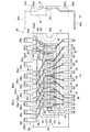
図1(a)および(b)は、それぞれ、本発明の一実施形態の半導体装置で、内部構造を説明する平面図および側面図である。図2〜図4は、何れも、本発明の一実施形態の半導体装置の変形例を示す部分拡大平面図である。 1A and 1B are a plan view and a side view, respectively, for explaining the internal structure of a semiconductor device according to an embodiment of the present invention. 2 to 4 are partially enlarged plan views showing modifications of the semiconductor device according to the embodiment of the present invention.
図1に示すように、半導体装置10は、放熱性の回路基板である放熱回路基板20と、放熱回路基板20に搭載された第1の発熱素子22、第2の発熱素子24、リードフレーム26および感温素子(例えばサーミスタ)28と、を備えている。
As shown in FIG. 1, the semiconductor device 10 includes a heat
第1の発熱素子22と第2の発熱素子24は、封止樹脂34の短手方向の略中央部に配置されている。また第1の発熱素子22は第2の発熱素子24よりも相対的に発熱が多い。
The first
半導体装置10は、放熱回路基板20の裏面が露出するように、これらを封止する封止樹脂34を備えている。
The semiconductor device 10 includes a
放熱回路基板(放熱板)20は、金属ベース回路基板やセラミックベース回路基板であることが多い。また、放熱回路基板20上の銅パターン部分(図示せず)と、第2の発熱素子24を搭載したリードフレーム26の裏面とが、導電性接着剤(例えばはんだ)を介して接着され、放熱回路基板20の裏面は、封止樹脂(封止体)34から露出している。
The heat dissipation circuit board (heat dissipation plate) 20 is often a metal base circuit board or a ceramic base circuit board. In addition, a copper pattern portion (not shown) on the heat
(フレームタブ)
リードフレーム26は複数のフレームタブを有している。すなわち、リードフレーム26は、第1の発熱素子22を搭載する第1フレームタブ40と、第1の発熱素子22および第2の発熱素子24を搭載する第2フレームタブ42と、第2の発熱素子24を搭載する第3フレームタブ43とを有する。そして第2フレームタブ42には、第1の発熱素子22と第2の発熱素子24との間のフレームタブ部分42mに、フレームタブ部分42mを貫通する透孔46が形成されている。また、隣り合う第2の発熱素子24同士の間にも透孔46が形成されている。
(Frame tab)
The
本実施形態では、リードフレーム26は銅製であり、均一な厚さの平条フレームである。従ってフレームタブ(第1フレームタブ40、第2フレームタブ42、および、第3フレームタブ43)は銅からなる。フレームタブが導電性接着剤(例えばはんだ)で付けられる放熱回路基板20上の銅パターン部分(図示せず)のサイズは、フレームタブと接する部分に比べ、同じか或いはやや小さくされている。
In the present embodiment, the
また、第1フレームタブ40における第1の発熱素子22の1つあたりの面積は、第2フレームタブ42における第2の発熱素子24の1つあたりの面積に比べて大きい。具体的には、第1フレームタブ40の熱抵抗が、第2フレームタブ42の熱抵抗よりも小さくなるように、第1フレームタブ40の第1の発熱素子1つあたりの面積を、第2フレームタブ42の第2の発熱素子1つあたりの面積に比べて例えば1.5倍以上大きくすることにより、第1の発熱素子22からの熱を効率良く放熱できる構造になっている。なお、第1の発熱素子22の熱抵抗は1.7W/℃、第2の発熱素子24の熱抵抗は3W/℃である。
In addition, the area of each
(インナーリード)
リードフレーム26を構成するインナーリード26iはアウターリード26eに連続している。インナーリード26iのうち、第2フレームタブ42に接続するインナーリード以外では、インナーリードポスト26p1、26p2のいずれかを有する。インナーリードポスト26p1、26p2は平面視矩形状であり、その長手方向が、放熱回路基板20の長手方向に沿うように配置されている。インナーリードポスト26p1の長手方向略中央部には、第2の発熱素子24と電気接続するためのワイヤ(ボンディングワイヤ)W1が接続されている。そして、インナーリードポスト26p2の長手方向略中央部には、第1の発熱素子22と電気接続するためのワイヤ(ボンディングワイヤ)W2、W3が接続されている。なお、ワイヤの材質には例えばアルミニウムまたはアルミニウム合金、あるいは金または金合金、あるいは銅または銅合金を用いる。
(Inner lead)
また、本実施形態では、第2フレームタブ42には1つの第1の発熱素子22と複数(図1では3つ)の第2の発熱素子24とが配置されており、第3フレームタブ43には1つの第2の発熱素子24が配置されている。このため、第2フレームタブ42に供給する電力は第3フレームタブに供給する電力に比べて大きい。本実施形態ではこれを考慮して、アウターリード26eと第2フレームタブ42とに接続するインナーリード本体26mの横幅が、インナーリードポスト26p1と第3フレームタブ43とに接続するインナーリード接続部26cnに比べて幅広にされている。
Further, in the present embodiment, one first
また、本実施形態では、図1から判るように、第3フレームタブ43に接続するインナーリード接続部26cnと、第2の発熱素子24に接続されるワイヤW1とは、平面視で互い違いに交差している。
In the present embodiment, as can be seen from FIG. 1, the inner
(封止樹脂)
本実施形態では、封止樹脂34は、放熱回路基板20と対向する側の長手方向、すなわち放熱回路基板20に接する側が放熱回路基板20に対して確実に凸形状となるように(すなわち封止樹脂34の表面側が凹形状となるように)、封止樹脂34の線膨張率、封止樹脂34の厚み、放熱回路基板20の厚みなどが考慮されている。
(Sealing resin)
In this embodiment, the
また、封止樹脂34の裏面に切欠部34dを形成することで沿面距離を確保しており、これにより、電気絶縁性が向上している。
Moreover, the creepage distance is ensured by forming the
また、封止樹脂34の長手方向両端部には、ビス止めのネジが入り込む切欠部34sが形成されている。そして、平面視の投影面上で、ビス止めのネジの頭部Hが、第1の発熱素子22、更にはリードフレーム26に重ならないように、切欠部34s、リードフレーム26などの寸法、位置が決められている。
Further,
(アウターリード)
また、本実施形態では、インナーリード26iに連続するアウターリード26eは、放熱回路基板20の外周から内側で曲げて、放熱回路基板20の裏面から離す必要があり、放熱回路基板20とは高さを異ならせている。
(Outer lead)
In the present embodiment, the
本実施形態では、アウターリード26eは放熱回路基板20に繋がる部位がデプレスされていることで、このようにアウターリード26eの端部(樹脂封止体側面から導出されたアウターリードの端面)と放熱回路基板20との高さが異なっている。
In the present embodiment, the
また、本実施形態では、デプレスの位置は、放熱回路基板20を中央にして、左右同じであるが、異なっていてもよい。
Further, in this embodiment, the position of pressing is the same on the left and right with the heat
なお、デプレスの形態としては、例えば図1(b)に示すように、高さ方向に対して側面視で直線状に傾斜する直線傾斜部26es、26etを形成してもよく、デプレスの形態は特に限定しない。 In addition, as a form of pressing, for example, as shown in FIG. 1 (b), linear inclined portions 26es and 26et that are linearly inclined in a side view with respect to the height direction may be formed. There is no particular limitation.
(感温素子)
感温素子28は半導体素子を有するものであり、過熱保護用に放熱回路基板20上に載置され、検知能力が向上している。すなわち、図1に示すように、感温素子28は、放熱回路基板20に形成されている電極21k、21jに接続され、放熱回路基板20上に直接に載置されているので、フレームタブを介して感温素子を配置した場合に比べ、放熱回路基板20の温度を高い検出精度で検出をすることができる構成になっている。
(Temperature sensor)
The
また感温素子28は、発熱素子と同様に封止樹脂34の短手方向の略中央部に配置され、また隣り合う第3フレームタブ43同士の間隔と同一の間隔で、第2の発熱素子24の横並びに配置されている。
Similarly to the heat generating element, the temperature
また、感温素子28は、長矩形の外形を有し、感温素子28の長手方向が半導体装置10の長手方向と垂直になるよう配置しており、歪による特性変動を防止している。
Further, the
また、本実施形態では、感温素子28に接続される放熱回路基板20の電極面積(一方の電極21jおよび他方の電極21kの合計の面積)が、感温素子28の平面視面積よりも広い。
In the present embodiment, the electrode area of the heat
(作用、効果)
以下、本実施形態の作用、効果について説明する。
(Function, effect)
Hereinafter, the operation and effect of the present embodiment will be described.
本実施形態では、感温素子28が放熱回路基板20上に直接に載置されている。従って、支持板などの介在物を経由して感温素子を配置した従来例に比べ、放熱回路基板20の温度を高い検出精度で温度検出をすることができ、充分な過熱対策保護を図ることができる。
In the present embodiment, the temperature
また、本実施形態では、感温素子28に接続される放熱回路基板20の電極面積(一方の電極21jおよび他方の電極21kの合計の面積)が、感温素子28の平面視面積は、従来に比べて遥かに広い。従って、放熱回路基板20の熱が感温素子28に伝わる速度は、従来に比べて遥かに速く、放熱回路基板20の温度をより迅速に正確に検出することができる。
In this embodiment, the electrode area of the heat
また感温素子28は、発熱素子と同様に封止樹脂34の短手方向の略中央部に配置されている。そして、感温素子28は、隣り合う第3フレームタブ43の間隔と同一の間隔で第2の発熱素子24の横並びの位置に配置されており、このように感温素子28が第2の発熱素子24に隣接することで、更に検出精度を向上させることができる構成になっている。
Further, the temperature-
また、感温素子28は、長矩形の外形を有し、感温素子28の長手方向が半導体装置10の長手方向と垂直になるよう配置しており、歪による特性変動を防止している。すなわち、温度変化などにより封止樹脂34に反りが生じた場合、仮に感温素子28の長手方向が半導体装置10の長手方向と平行であると、感温素子28に生じる反りが最大となるが、本実施形態では、封止樹脂34の反りによって感温素子28に生じる反りが最小となるように感温素子28の向きが設定されている。
Further, the
また、インナーリードポスト26p1と第2の発熱素子24が載置される第3フレームタブ43とに連続するインナーリード接続部26cnと、インナーリードポスト26p1と第2の発熱素子24とに接続するワイヤ(ボンディングワイヤ)W1とは、平面視で交差した、いわゆるクロス配線となっており、しかも、互い違いにクロスしている。これにより、接続に必要な領域を狭くすることができ、半導体装置10の小型化に大きく役立っている。また、小型化のために、アウターリードのピッチが狭い場合でも、接続に必要な領域を狭くすることができ、狭ピッチに対応することが可能である。
In addition, the inner lead connection portion 26cn continuous to the inner lead post 26p1 and the
また、インナーリード接続部26cnの幅を広くすることにより、放熱性の向上が期待できる。 Further, by increasing the width of the inner lead connection portion 26cn, it is possible to expect improvement in heat dissipation.
また、インナーリード接続部26cnの厚さを厚くして放熱性の向上が期待できる。 Further, the heat dissipation can be improved by increasing the thickness of the inner lead connection portion 26cn.
また、インナーリード接続部26cnの幅を広くしたり、あるいは厚さを厚くしたりすることでインナーリード接続部26cnの機械的強度が向上し、変形を防止する効果が期待できる。 Further, by increasing the width of the inner lead connection portion 26cn or increasing the thickness, the mechanical strength of the inner lead connection portion 26cn is improved, and an effect of preventing deformation can be expected.
また、インナーリード26iに形成されたインナーリードポスト26p1、26p2は、平面視矩形状であって、その長手方向が、放熱回路基板20の長手方向と平行方向となるように配置されている。インナーリードポスト26p1には第2の発熱素子24と電気接続するためのワイヤ(ボンディング)W1が接続されている。従って、ワイヤボンディングする際にインナーリードポスト26p1の両端部を押さえて確実にワイヤボンディングすることができる。しかも、半導体装置10の小型化を図るために第1の発熱素子22を密集させた配置にしても、上記のクロス配線の領域を確保することができ、半導体装置10の小型化を充分に図り易い。インナーリードポスト26p2についても同様である。
The inner lead posts 26p1 and 26p2 formed on the
また、ワイヤの材質は、通電のために電気抵抗の低い金属が好ましく、例えばアルミニウムまたはアルミニウム合金、あるいは金または金合金、あるいは銅または銅合金が好ましい。 Further, the material of the wire is preferably a metal having a low electric resistance for energization, and for example, aluminum or aluminum alloy, gold or gold alloy, or copper or copper alloy is preferable.
また、ワイヤの太さについては、大電流を流すワイヤは電気抵抗を小さくするために相対的に太く、それ以外のワイヤは細くしてもよい。 Further, regarding the thickness of the wire, the wire through which a large current flows may be relatively thick in order to reduce the electric resistance, and the other wires may be thin.
また、リボンワイヤあるいは、ストラップリードを用いることによって、高い通電性と放熱性の向上を期待することができる。 Further, by using a ribbon wire or a strap lead, it is possible to expect an improvement in high electrical conductivity and heat dissipation.
また、リードフレーム26は複数のフレームタブ(第1フレームタブ40および第2フレームタブ42)を有しており、第1フレームタブ40における第1の発熱素子22の1つあたりの面積は、第2フレームタブ42における第2の発熱素子24の1つあたりの面積に比べて大きい。従って、第1フレームタブ40では第2フレームタブ42よりも放熱し易いので、第1の発熱素子22で発生した熱を放熱し易い。
Further, the
また、第2フレームタブ42には、1つの第1の発熱素子22と複数の第2の発熱素子24とが配置されており、第2フレームタブ42に供給する電力は他のフレームタブに比べて相対的に大きい。アウターリード26eと第2フレームタブ42とに接続するインナーリード本体26mの横幅を幅広にすることで伝熱効果を高め放熱性を向上させることができる。
The
また、第2フレームタブ42の透孔46は、第2フレームタブ42の横方向の熱伝導を妨げることにより、発熱素子間の熱の影響を防止することには有効であるが、第2フレームタブ42の中央付近に熱がこもり易くなることを防ぐため、幅広なインナーリード本体26mを第2フレームタブ42の略中央に接続することにより、第2フレームタブ42の放熱性を向上させることができる。
Further, the through
また、第1の発熱素子22と第2の発熱素子24との間のフレームタブ部分42mに、フレームタブ部分42mを貫通する透孔46が形成されている。
Further, a through
透孔46により、フレームタブ部分42mを通過する横方向の伝熱を防止でき、第1の発熱素子22で発生した熱が、第2の発熱素子24に伝わることを防止できる。
The through holes 46 can prevent lateral heat transfer through the
また、透孔46内には第2フレームタブ40を放熱回路基板に接着する際に、樹脂を主剤とした導電性接着剤が入り込んでもよい。この場合、はんだが入り込んだ場合よりも熱の遮断性効果が高くなる。
In addition, when the
また、封止樹脂34にて封止した際に封止樹脂34が入り込んでも熱の遮断性効果が高くなる。この際、透孔46内にボイド等の空気が入り込んでも熱の遮断性効果が高くなる。
Moreover, even if the sealing
なお、導電性接着剤として、はんだを入り込ませてもよい。この場合、熱の遮断性は劣るが、接着時にはんだ中のボイドが透孔46内に抜けるため、はんだの厚みを均一化しやすいという効果が得られる。
Note that solder may be inserted as the conductive adhesive. In this case, the heat shielding property is inferior, but since the voids in the solder come out into the through-
また透孔46の形状、大きさは本実施形態に限定するものでは無く、第2フレームタブの強度が維持される大きさであればよい。
The shape and size of the through
例えば、透孔46の幅は、フレームタブ部分42mの幅と略等しい幅まで可能である。
For example, the width of the through
また、フレームタブの厚みが均一な平条フレームとしたが、フレームタブが厚い異形条フレームとすることで熱容量が増加し、放熱効果を向上させることができる。 Further, although the flat strip frame has a uniform thickness of the frame tab, the heat capacity can be increased and the heat dissipation effect can be improved by using a deformed strip frame having a thick frame tab.
フレームタブが導電性接着剤(例えばはんだ)で付けられる放熱回路基板20上の銅パターン部分(図示せず)のサイズは、フレームタブと接する部分に比べ、同じか或いはやや小さくされており、これにより、導電性接着剤(例えばはんだ)のはみ出しが抑えられている。
The size of the copper pattern portion (not shown) on the heat
なお、リードフレーム26の表面にはめっき(例えばニッケルめっき)を施してもよい。
Note that the surface of the
放熱回路基板20は、放熱性を重視する場合は金属ベース回路基板とし、そうでない場合は、安価なセラミックベース回路基板することができる。
The heat dissipating
また、放熱回路基板20は、放熱回路基板20上の銅パターン部分に、第2の発熱素子24を搭載したリードフレーム26の裏面を導電性接着剤(例えばはんだ)を介して接着しており、発熱素子からの熱を封止樹脂34から露出した放熱回路基板20の裏面から放熱する効果が期待できる。
Further, the heat
また、銅パターン部分のサイズは、フレームタブと接する部分に比べ、同じか或いはやや小さくされており、これにより、導電性接着剤のはみ出しが抑えられている。 Further, the size of the copper pattern portion is the same as or slightly smaller than that of the portion in contact with the frame tab, thereby preventing the conductive adhesive from protruding.
また、封止樹脂34は、放熱回路基板20と対向する側の長手方向、すなわち放熱回路基板20に接する側が放熱回路基板20に対して確実に凸形状となっている。これにより、外部の放熱フィンにビス止めすることで、放熱回路基板20の中央部が封止樹脂34から浮き上がることを確実に防止し、密着性を向上させることができる。このことは、封止樹脂34が薄厚であるときに特に顕著な効果を奏する。
Further, the sealing
また、封止樹脂34の裏面に切欠部34dを形成することで沿面距離を確保しており、これにより、電気絶縁性が向上している。
Moreover, the creepage distance is ensured by forming the
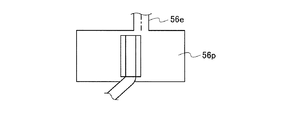
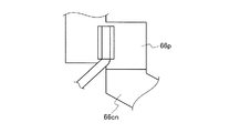
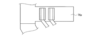
なお、インナーリードポスト26p1、26p2とアウターリード26eやインナーリード接続部26cnとの接続形態や、インナーリードポスト26p1、26p2の寸法などは特に限定するものではない。例えば、図1に示したアウターリード26eよりも幅細のアウターリード56e(図2参照)が接続されたインナーリードポスト56pであってもよいし、図1に示したインナーリード接続部26cnに比べ、平面視で逆方向(紙面左下方向)に延び出すインナーリード接続部66cn(図3参照)が接続されたインナーリードポスト66pであってもよい。また、図1に示したインナーリードポスト26p2に比べ、平面視での縦横比が更に大きいインナーリードポスト76p(図4参照)であってもよい。
The connection form between the inner lead posts 26p1 and 26p2 and the outer leads 26e and the inner lead connection portion 26cn, the dimensions of the inner lead posts 26p1 and 26p2, and the like are not particularly limited. For example, the inner
また、本実施形態では、感温素子28の長手方向が半導体装置10の長手方向と垂直になるよう配置された例で説明したが、厳密に垂直ではなくて、例えば垂直方向に対して±5°程度に傾いていても、封止樹脂34の反りによって感温素子28に生じる反りを小さくすることができる。
Further, in the present embodiment, the example in which the longitudinal direction of the
また、本実施形態では、インナーリードポスト26p1、26p2の長手方向が、放熱回路基板20の長手方向と平行方向となるように配置された例で説明したが、厳密に平行ではなくて、例えば平行方向に対して±5°程度に傾いていても、ワイヤボンディングする際にインナーリードポスト26p1の両端部を押さえて確実にワイヤボンディングすることができ、また、第1の発熱素子22を密集させた配置にしても、上記のクロス配線の領域を確保して半導体装置10の小型化を充分に図ることができる。
In the present embodiment, the example in which the inner lead posts 26p1 and 26p2 are arranged so that the longitudinal direction thereof is parallel to the longitudinal direction of the heat
感温素子28は、温度検知精度に応じた電子部品や抵抗で構成することもできる。
The
第1の発熱素子22と第2の発熱素子24は、従来のシリコン(Si)半導体素子に比べて高温状態での動作が可能であり、スイッチング速度が速く、低損失である化合物半導体、例えばシリコンカーバイド(SiC)やガリウムナイトライド(GaN)等の化合物半導体で構成することもできる。
The first
以上のように、本発明に係る半導体装置は、インナーリードは、ボンディングワイヤの被接続部となるインナーリードポストを有しており、インナーリードポストは、矩形状であって長手方向が放熱回路基板の長手方向に沿っているので、装置の小型化を図りつつインナーリードにワイヤボンディングを良好に行うことができる構成の半導体装置として用いるのに好適である。 As described above, in the semiconductor device according to the present invention, the inner lead has the inner lead post that becomes the connected portion of the bonding wire, and the inner lead post is rectangular and the longitudinal direction is the heat dissipation circuit board. Therefore, it is suitable for use as a semiconductor device having a configuration in which wire bonding can be satisfactorily performed on the inner lead while reducing the size of the device.
10 半導体装置
20 放熱回路基板
22 発熱素子
24 発熱素子
26 リードフレーム
26cn インナーリード接続部
26m インナーリード本体
26p1 インナーリードポスト
26p2 インナーリードポスト
40 第1フレームタブ(単数素子搭載フレームタブ)
42 第2フレームタブ(複数素子搭載フレームタブ)
43 第3フレームタブ(単数素子搭載フレームタブ)
W1 ワイヤ(ボンディングワイヤ)
W2 ワイヤ(ボンディングワイヤ)
W3 ワイヤ(ボンディングワイヤ)
DESCRIPTION OF SYMBOLS 10
42 2nd frame tab (multi-element mounting frame tab)
43 3rd Frame Tab (Single Element Mounted Frame Tab)
W1 wire (bonding wire)
W2 wire (bonding wire)
W3 wire (bonding wire)
Claims (4)
前記インナーリードは、ボンディングワイヤの被接続部となるインナーリードポストを有しており、
前記インナーリードポストは、矩形状であって長手方向が前記放熱回路基板の長手方向に沿っていることを特徴とする半導体装置。 A semiconductor device having an inner lead on a heat dissipation circuit board,
The inner lead has an inner lead post that becomes a connected portion of a bonding wire,
The semiconductor device according to claim 1, wherein the inner lead post has a rectangular shape and a longitudinal direction thereof is along a longitudinal direction of the heat dissipation circuit board.
前記インナーリードポストと前記フレームタブとに連続するインナーリード接続部と、前記インナーリードポストと前記フレームタブ上に載置された前記発熱素子とに接続するボンディングワイヤとは、平面視で交差していることを特徴とする請求項1または2記載の半導体装置。 The lead frame having the inner lead includes a frame tab on which the heating element is placed,
An inner lead connecting portion continuous to the inner lead post and the frame tab, and a bonding wire connected to the inner lead post and the heating element placed on the frame tab intersect in plan view. The semiconductor device according to claim 1, wherein the semiconductor device is a semiconductor device.
前記複数素子搭載フレームタブに接続する前記インナーリード接続部またはインナーリード本体は、前記単数素子搭載フレームタブに接続する前記インナーリード接続部に比べて幅広であることを特徴とする請求項3記載の半導体装置。 As the frame tab, a single element mounting frame tab on which one heating element is mounted, and a multiple element mounting frame tab on which a plurality of heating elements are mounted, are provided.
The inner lead connecting portion or the inner lead main body connected to the multi-element mounting frame tab is wider than the inner lead connecting portion connected to the single element mounting frame tab. Semiconductor device.
Priority Applications (1)
| Application Number | Priority Date | Filing Date | Title |
|---|---|---|---|
| JP2013073507A JP2014123701A (en) | 2012-11-20 | 2013-03-29 | Semiconductor device |
Applications Claiming Priority (3)
| Application Number | Priority Date | Filing Date | Title |
|---|---|---|---|
| JP2012254552 | 2012-11-20 | ||
| JP2012254552 | 2012-11-20 | ||
| JP2013073507A JP2014123701A (en) | 2012-11-20 | 2013-03-29 | Semiconductor device |
Publications (1)
| Publication Number | Publication Date |
|---|---|
| JP2014123701A true JP2014123701A (en) | 2014-07-03 |
Family
ID=51403948
Family Applications (2)
| Application Number | Title | Priority Date | Filing Date |
|---|---|---|---|
| JP2013073507A Pending JP2014123701A (en) | 2012-11-20 | 2013-03-29 | Semiconductor device |
| JP2013073495A Pending JP2014123700A (en) | 2012-11-20 | 2013-03-29 | Semiconductor device |
Family Applications After (1)
| Application Number | Title | Priority Date | Filing Date |
|---|---|---|---|
| JP2013073495A Pending JP2014123700A (en) | 2012-11-20 | 2013-03-29 | Semiconductor device |
Country Status (1)
| Country | Link |
|---|---|
| JP (2) | JP2014123701A (en) |
Families Citing this family (2)
| Publication number | Priority date | Publication date | Assignee | Title |
|---|---|---|---|---|
| WO2021251126A1 (en) * | 2020-06-08 | 2021-12-16 | ローム株式会社 | Semiconductor device |
| CN114035643A (en) * | 2022-01-10 | 2022-02-11 | 上海奥简微电子科技有限公司 | Temperature control protection circuit |
-
2013
- 2013-03-29 JP JP2013073507A patent/JP2014123701A/en active Pending
- 2013-03-29 JP JP2013073495A patent/JP2014123700A/en active Pending
Also Published As
| Publication number | Publication date |
|---|---|
| JP2014123700A (en) | 2014-07-03 |
Similar Documents
| Publication | Publication Date | Title |
|---|---|---|
| US7755179B2 (en) | Semiconductor package structure having enhanced thermal dissipation characteristics | |
| JP7150461B2 (en) | semiconductor equipment | |
| JP6164364B2 (en) | Semiconductor device | |
| KR101477378B1 (en) | Housing and power module having the same | |
| CN112514066B (en) | Semiconductor devices | |
| JP6448418B2 (en) | Power semiconductor device | |
| JP7238353B2 (en) | Semiconductor module and semiconductor device using the same | |
| JP7121188B2 (en) | Element substrate, light-emitting element module, and light-emitting device | |
| WO2014034411A1 (en) | Electric power semiconductor device | |
| JP2015115471A (en) | Power semiconductor device | |
| JP7379886B2 (en) | semiconductor equipment | |
| JP6048238B2 (en) | Electronic equipment | |
| US20130147027A1 (en) | Semiconductor package | |
| JP6540587B2 (en) | Power module | |
| JP4702279B2 (en) | Semiconductor device and manufacturing method thereof | |
| JP4046623B2 (en) | Power semiconductor module and fixing method thereof | |
| JP5429413B2 (en) | Semiconductor device | |
| JP2014123701A (en) | Semiconductor device | |
| JP5177174B2 (en) | Semiconductor device | |
| JP2013113638A (en) | Semiconductor device | |
| JP2008091432A (en) | Electronic components | |
| JP2015149363A (en) | Semiconductor module | |
| JP2014103270A (en) | Semiconductor module | |
| JP6060053B2 (en) | Power semiconductor device | |
| KR101897304B1 (en) | Power module |