JP2014123736A - Semiconductor package - Google Patents
Semiconductor package Download PDFInfo
- Publication number
- JP2014123736A JP2014123736A JP2013263323A JP2013263323A JP2014123736A JP 2014123736 A JP2014123736 A JP 2014123736A JP 2013263323 A JP2013263323 A JP 2013263323A JP 2013263323 A JP2013263323 A JP 2013263323A JP 2014123736 A JP2014123736 A JP 2014123736A
- Authority
- JP
- Japan
- Prior art keywords
- semiconductor chip
- bonding pad
- semiconductor
- disposed
- package
- Prior art date
- Legal status (The legal status is an assumption and is not a legal conclusion. Google has not performed a legal analysis and makes no representation as to the accuracy of the status listed.)
- Withdrawn
Links
Images

Classifications
-
- H—ELECTRICITY
- H10—SEMICONDUCTOR DEVICES; ELECTRIC SOLID-STATE DEVICES NOT OTHERWISE PROVIDED FOR
- H10W—GENERIC PACKAGES, INTERCONNECTIONS, CONNECTORS OR OTHER CONSTRUCTIONAL DETAILS OF DEVICES COVERED BY CLASS H10
- H10W90/00—Package configurations
-
- H—ELECTRICITY
- H10—SEMICONDUCTOR DEVICES; ELECTRIC SOLID-STATE DEVICES NOT OTHERWISE PROVIDED FOR
- H10W—GENERIC PACKAGES, INTERCONNECTIONS, CONNECTORS OR OTHER CONSTRUCTIONAL DETAILS OF DEVICES COVERED BY CLASS H10
- H10W72/00—Interconnections or connectors in packages
-
- H—ELECTRICITY
- H10—SEMICONDUCTOR DEVICES; ELECTRIC SOLID-STATE DEVICES NOT OTHERWISE PROVIDED FOR
- H10W—GENERIC PACKAGES, INTERCONNECTIONS, CONNECTORS OR OTHER CONSTRUCTIONAL DETAILS OF DEVICES COVERED BY CLASS H10
- H10W70/00—Package substrates; Interposers; Redistribution layers [RDL]
- H10W70/60—Insulating or insulated package substrates; Interposers; Redistribution layers
- H10W70/62—Insulating or insulated package substrates; Interposers; Redistribution layers characterised by their interconnections
- H10W70/63—Vias, e.g. via plugs
-
- H—ELECTRICITY
- H10—SEMICONDUCTOR DEVICES; ELECTRIC SOLID-STATE DEVICES NOT OTHERWISE PROVIDED FOR
- H10W—GENERIC PACKAGES, INTERCONNECTIONS, CONNECTORS OR OTHER CONSTRUCTIONAL DETAILS OF DEVICES COVERED BY CLASS H10
- H10W70/00—Package substrates; Interposers; Redistribution layers [RDL]
- H10W70/60—Insulating or insulated package substrates; Interposers; Redistribution layers
- H10W70/62—Insulating or insulated package substrates; Interposers; Redistribution layers characterised by their interconnections
- H10W70/65—Shapes or dispositions of interconnections
-
- H—ELECTRICITY
- H10—SEMICONDUCTOR DEVICES; ELECTRIC SOLID-STATE DEVICES NOT OTHERWISE PROVIDED FOR
- H10W—GENERIC PACKAGES, INTERCONNECTIONS, CONNECTORS OR OTHER CONSTRUCTIONAL DETAILS OF DEVICES COVERED BY CLASS H10
- H10W72/00—Interconnections or connectors in packages
- H10W72/20—Bump connectors, e.g. solder bumps or copper pillars; Dummy bumps; Thermal bumps
- H10W72/241—Dispositions, e.g. layouts
- H10W72/247—Dispositions of multiple bumps
- H10W72/248—Top-view layouts, e.g. mirror arrays
-
- H—ELECTRICITY
- H10—SEMICONDUCTOR DEVICES; ELECTRIC SOLID-STATE DEVICES NOT OTHERWISE PROVIDED FOR
- H10W—GENERIC PACKAGES, INTERCONNECTIONS, CONNECTORS OR OTHER CONSTRUCTIONAL DETAILS OF DEVICES COVERED BY CLASS H10
- H10W72/00—Interconnections or connectors in packages
- H10W72/20—Bump connectors, e.g. solder bumps or copper pillars; Dummy bumps; Thermal bumps
- H10W72/261—Functions other than electrical connecting
- H10W72/263—Providing mechanical bonding or support, e.g. dummy bumps
-
- H—ELECTRICITY
- H10—SEMICONDUCTOR DEVICES; ELECTRIC SOLID-STATE DEVICES NOT OTHERWISE PROVIDED FOR
- H10W—GENERIC PACKAGES, INTERCONNECTIONS, CONNECTORS OR OTHER CONSTRUCTIONAL DETAILS OF DEVICES COVERED BY CLASS H10
- H10W72/00—Interconnections or connectors in packages
- H10W72/20—Bump connectors, e.g. solder bumps or copper pillars; Dummy bumps; Thermal bumps
- H10W72/261—Functions other than electrical connecting
- H10W72/267—Multiple bump connectors having different functions
-
- H—ELECTRICITY
- H10—SEMICONDUCTOR DEVICES; ELECTRIC SOLID-STATE DEVICES NOT OTHERWISE PROVIDED FOR
- H10W—GENERIC PACKAGES, INTERCONNECTIONS, CONNECTORS OR OTHER CONSTRUCTIONAL DETAILS OF DEVICES COVERED BY CLASS H10
- H10W72/00—Interconnections or connectors in packages
- H10W72/20—Bump connectors, e.g. solder bumps or copper pillars; Dummy bumps; Thermal bumps
- H10W72/29—Bond pads specially adapted therefor
-
- H—ELECTRICITY
- H10—SEMICONDUCTOR DEVICES; ELECTRIC SOLID-STATE DEVICES NOT OTHERWISE PROVIDED FOR
- H10W—GENERIC PACKAGES, INTERCONNECTIONS, CONNECTORS OR OTHER CONSTRUCTIONAL DETAILS OF DEVICES COVERED BY CLASS H10
- H10W72/00—Interconnections or connectors in packages
- H10W72/30—Die-attach connectors
- H10W72/351—Materials of die-attach connectors
- H10W72/353—Materials of die-attach connectors not comprising solid metals or solid metalloids, e.g. ceramics
- H10W72/354—Materials of die-attach connectors not comprising solid metals or solid metalloids, e.g. ceramics comprising polymers
-
- H—ELECTRICITY
- H10—SEMICONDUCTOR DEVICES; ELECTRIC SOLID-STATE DEVICES NOT OTHERWISE PROVIDED FOR
- H10W—GENERIC PACKAGES, INTERCONNECTIONS, CONNECTORS OR OTHER CONSTRUCTIONAL DETAILS OF DEVICES COVERED BY CLASS H10
- H10W72/00—Interconnections or connectors in packages
- H10W72/50—Bond wires
- H10W72/541—Dispositions of bond wires
- H10W72/5453—Dispositions of bond wires connecting between multiple bond pads on a chip, e.g. daisy chain
-
- H—ELECTRICITY
- H10—SEMICONDUCTOR DEVICES; ELECTRIC SOLID-STATE DEVICES NOT OTHERWISE PROVIDED FOR
- H10W—GENERIC PACKAGES, INTERCONNECTIONS, CONNECTORS OR OTHER CONSTRUCTIONAL DETAILS OF DEVICES COVERED BY CLASS H10
- H10W72/00—Interconnections or connectors in packages
- H10W72/50—Bond wires
- H10W72/59—Bond pads specially adapted therefor
-
- H—ELECTRICITY
- H10—SEMICONDUCTOR DEVICES; ELECTRIC SOLID-STATE DEVICES NOT OTHERWISE PROVIDED FOR
- H10W—GENERIC PACKAGES, INTERCONNECTIONS, CONNECTORS OR OTHER CONSTRUCTIONAL DETAILS OF DEVICES COVERED BY CLASS H10
- H10W72/00—Interconnections or connectors in packages
- H10W72/851—Dispositions of multiple connectors or interconnections
- H10W72/853—On the same surface
- H10W72/859—Bump connectors and bond wires
-
- H—ELECTRICITY
- H10—SEMICONDUCTOR DEVICES; ELECTRIC SOLID-STATE DEVICES NOT OTHERWISE PROVIDED FOR
- H10W—GENERIC PACKAGES, INTERCONNECTIONS, CONNECTORS OR OTHER CONSTRUCTIONAL DETAILS OF DEVICES COVERED BY CLASS H10
- H10W72/00—Interconnections or connectors in packages
- H10W72/851—Dispositions of multiple connectors or interconnections
- H10W72/874—On different surfaces
- H10W72/884—Die-attach connectors and bond wires
-
- H—ELECTRICITY
- H10—SEMICONDUCTOR DEVICES; ELECTRIC SOLID-STATE DEVICES NOT OTHERWISE PROVIDED FOR
- H10W—GENERIC PACKAGES, INTERCONNECTIONS, CONNECTORS OR OTHER CONSTRUCTIONAL DETAILS OF DEVICES COVERED BY CLASS H10
- H10W72/00—Interconnections or connectors in packages
- H10W72/90—Bond pads, in general
- H10W72/931—Shapes of bond pads
- H10W72/932—Plan-view shape, i.e. in top view
-
- H—ELECTRICITY
- H10—SEMICONDUCTOR DEVICES; ELECTRIC SOLID-STATE DEVICES NOT OTHERWISE PROVIDED FOR
- H10W—GENERIC PACKAGES, INTERCONNECTIONS, CONNECTORS OR OTHER CONSTRUCTIONAL DETAILS OF DEVICES COVERED BY CLASS H10
- H10W72/00—Interconnections or connectors in packages
- H10W72/90—Bond pads, in general
- H10W72/941—Dispositions of bond pads
- H10W72/942—Dispositions of bond pads relative to underlying supporting features, e.g. bond pads, RDLs or vias
-
- H—ELECTRICITY
- H10—SEMICONDUCTOR DEVICES; ELECTRIC SOLID-STATE DEVICES NOT OTHERWISE PROVIDED FOR
- H10W—GENERIC PACKAGES, INTERCONNECTIONS, CONNECTORS OR OTHER CONSTRUCTIONAL DETAILS OF DEVICES COVERED BY CLASS H10
- H10W72/00—Interconnections or connectors in packages
- H10W72/90—Bond pads, in general
- H10W72/941—Dispositions of bond pads
- H10W72/944—Dispositions of multiple bond pads
- H10W72/9445—Top-view layouts, e.g. mirror arrays
-
- H—ELECTRICITY
- H10—SEMICONDUCTOR DEVICES; ELECTRIC SOLID-STATE DEVICES NOT OTHERWISE PROVIDED FOR
- H10W—GENERIC PACKAGES, INTERCONNECTIONS, CONNECTORS OR OTHER CONSTRUCTIONAL DETAILS OF DEVICES COVERED BY CLASS H10
- H10W74/00—Encapsulations, e.g. protective coatings
-
- H—ELECTRICITY
- H10—SEMICONDUCTOR DEVICES; ELECTRIC SOLID-STATE DEVICES NOT OTHERWISE PROVIDED FOR
- H10W—GENERIC PACKAGES, INTERCONNECTIONS, CONNECTORS OR OTHER CONSTRUCTIONAL DETAILS OF DEVICES COVERED BY CLASS H10
- H10W74/00—Encapsulations, e.g. protective coatings
- H10W74/10—Encapsulations, e.g. protective coatings characterised by their shape or disposition
- H10W74/111—Encapsulations, e.g. protective coatings characterised by their shape or disposition the semiconductor body being completely enclosed
- H10W74/114—Encapsulations, e.g. protective coatings characterised by their shape or disposition the semiconductor body being completely enclosed by a substrate and the encapsulations
- H10W74/117—Encapsulations, e.g. protective coatings characterised by their shape or disposition the semiconductor body being completely enclosed by a substrate and the encapsulations the substrate having spherical bumps for external connection
-
- H—ELECTRICITY
- H10—SEMICONDUCTOR DEVICES; ELECTRIC SOLID-STATE DEVICES NOT OTHERWISE PROVIDED FOR
- H10W—GENERIC PACKAGES, INTERCONNECTIONS, CONNECTORS OR OTHER CONSTRUCTIONAL DETAILS OF DEVICES COVERED BY CLASS H10
- H10W90/00—Package configurations
- H10W90/20—Configurations of stacked chips
-
- H—ELECTRICITY
- H10—SEMICONDUCTOR DEVICES; ELECTRIC SOLID-STATE DEVICES NOT OTHERWISE PROVIDED FOR
- H10W—GENERIC PACKAGES, INTERCONNECTIONS, CONNECTORS OR OTHER CONSTRUCTIONAL DETAILS OF DEVICES COVERED BY CLASS H10
- H10W90/00—Package configurations
- H10W90/20—Configurations of stacked chips
- H10W90/22—Configurations of stacked chips the stacked chips being on both top and bottom sides of a package substrate, interposer or RDL
-
- H—ELECTRICITY
- H10—SEMICONDUCTOR DEVICES; ELECTRIC SOLID-STATE DEVICES NOT OTHERWISE PROVIDED FOR
- H10W—GENERIC PACKAGES, INTERCONNECTIONS, CONNECTORS OR OTHER CONSTRUCTIONAL DETAILS OF DEVICES COVERED BY CLASS H10
- H10W90/00—Package configurations
- H10W90/20—Configurations of stacked chips
- H10W90/24—Configurations of stacked chips at least one of the stacked chips being laterally offset from a neighbouring stacked chip, e.g. chip stacks having a staircase shape
-
- H—ELECTRICITY
- H10—SEMICONDUCTOR DEVICES; ELECTRIC SOLID-STATE DEVICES NOT OTHERWISE PROVIDED FOR
- H10W—GENERIC PACKAGES, INTERCONNECTIONS, CONNECTORS OR OTHER CONSTRUCTIONAL DETAILS OF DEVICES COVERED BY CLASS H10
- H10W90/00—Package configurations
- H10W90/20—Configurations of stacked chips
- H10W90/26—Configurations of stacked chips the stacked chips being of the same size without any chips being laterally offset, e.g. chip stacks having a rectangular shape
-
- H—ELECTRICITY
- H10—SEMICONDUCTOR DEVICES; ELECTRIC SOLID-STATE DEVICES NOT OTHERWISE PROVIDED FOR
- H10W—GENERIC PACKAGES, INTERCONNECTIONS, CONNECTORS OR OTHER CONSTRUCTIONAL DETAILS OF DEVICES COVERED BY CLASS H10
- H10W90/00—Package configurations
- H10W90/20—Configurations of stacked chips
- H10W90/297—Configurations of stacked chips characterised by the through-semiconductor vias [TSVs] in the stacked chips
-
- H—ELECTRICITY
- H10—SEMICONDUCTOR DEVICES; ELECTRIC SOLID-STATE DEVICES NOT OTHERWISE PROVIDED FOR
- H10W—GENERIC PACKAGES, INTERCONNECTIONS, CONNECTORS OR OTHER CONSTRUCTIONAL DETAILS OF DEVICES COVERED BY CLASS H10
- H10W90/00—Package configurations
- H10W90/701—Package configurations characterised by the relative positions of pads or connectors relative to package parts
- H10W90/721—Package configurations characterised by the relative positions of pads or connectors relative to package parts of bump connectors
- H10W90/722—Package configurations characterised by the relative positions of pads or connectors relative to package parts of bump connectors between stacked chips
-
- H—ELECTRICITY
- H10—SEMICONDUCTOR DEVICES; ELECTRIC SOLID-STATE DEVICES NOT OTHERWISE PROVIDED FOR
- H10W—GENERIC PACKAGES, INTERCONNECTIONS, CONNECTORS OR OTHER CONSTRUCTIONAL DETAILS OF DEVICES COVERED BY CLASS H10
- H10W90/00—Package configurations
- H10W90/701—Package configurations characterised by the relative positions of pads or connectors relative to package parts
- H10W90/721—Package configurations characterised by the relative positions of pads or connectors relative to package parts of bump connectors
- H10W90/724—Package configurations characterised by the relative positions of pads or connectors relative to package parts of bump connectors between a chip and a stacked insulating package substrate, interposer or RDL
-
- H—ELECTRICITY
- H10—SEMICONDUCTOR DEVICES; ELECTRIC SOLID-STATE DEVICES NOT OTHERWISE PROVIDED FOR
- H10W—GENERIC PACKAGES, INTERCONNECTIONS, CONNECTORS OR OTHER CONSTRUCTIONAL DETAILS OF DEVICES COVERED BY CLASS H10
- H10W90/00—Package configurations
- H10W90/701—Package configurations characterised by the relative positions of pads or connectors relative to package parts
- H10W90/731—Package configurations characterised by the relative positions of pads or connectors relative to package parts of die-attach connectors
- H10W90/732—Package configurations characterised by the relative positions of pads or connectors relative to package parts of die-attach connectors between stacked chips
-
- H—ELECTRICITY
- H10—SEMICONDUCTOR DEVICES; ELECTRIC SOLID-STATE DEVICES NOT OTHERWISE PROVIDED FOR
- H10W—GENERIC PACKAGES, INTERCONNECTIONS, CONNECTORS OR OTHER CONSTRUCTIONAL DETAILS OF DEVICES COVERED BY CLASS H10
- H10W90/00—Package configurations
- H10W90/701—Package configurations characterised by the relative positions of pads or connectors relative to package parts
- H10W90/731—Package configurations characterised by the relative positions of pads or connectors relative to package parts of die-attach connectors
- H10W90/734—Package configurations characterised by the relative positions of pads or connectors relative to package parts of die-attach connectors between a chip and a stacked insulating package substrate, interposer or RDL
-
- H—ELECTRICITY
- H10—SEMICONDUCTOR DEVICES; ELECTRIC SOLID-STATE DEVICES NOT OTHERWISE PROVIDED FOR
- H10W—GENERIC PACKAGES, INTERCONNECTIONS, CONNECTORS OR OTHER CONSTRUCTIONAL DETAILS OF DEVICES COVERED BY CLASS H10
- H10W90/00—Package configurations
- H10W90/701—Package configurations characterised by the relative positions of pads or connectors relative to package parts
- H10W90/751—Package configurations characterised by the relative positions of pads or connectors relative to package parts of bond wires
- H10W90/752—Package configurations characterised by the relative positions of pads or connectors relative to package parts of bond wires between stacked chips
-
- H—ELECTRICITY
- H10—SEMICONDUCTOR DEVICES; ELECTRIC SOLID-STATE DEVICES NOT OTHERWISE PROVIDED FOR
- H10W—GENERIC PACKAGES, INTERCONNECTIONS, CONNECTORS OR OTHER CONSTRUCTIONAL DETAILS OF DEVICES COVERED BY CLASS H10
- H10W90/00—Package configurations
- H10W90/701—Package configurations characterised by the relative positions of pads or connectors relative to package parts
- H10W90/751—Package configurations characterised by the relative positions of pads or connectors relative to package parts of bond wires
- H10W90/754—Package configurations characterised by the relative positions of pads or connectors relative to package parts of bond wires between a chip and a stacked insulating package substrate, interposer or RDL
Landscapes
- Semiconductor Integrated Circuits (AREA)
- Internal Circuitry In Semiconductor Integrated Circuit Devices (AREA)
Abstract
【課題】電気的な特性が向上された半導体パッケージを提供する。
【解決手段】本発明による半導体パッケージは、その中央に開口部を有し、開口部に隣接して回路パターンを有するパッケージ基板と、前記パッケージ基板上に第1ボンディングパッドを有する第1半導体チップと、前記パッケージ基板と前記第1半導体チップとの間に実装され第2ボンディングパッドを有して互いに離隔された一対の第2半導体チップと、前記第1ボンディングパッドと前記第2ボンディングパッドとを電気的に接続する接続部材とを有する。
【選択図】 図2AA semiconductor package with improved electrical characteristics is provided.
A semiconductor package according to the present invention includes a package substrate having an opening at the center thereof and having a circuit pattern adjacent to the opening, and a first semiconductor chip having a first bonding pad on the package substrate. A pair of second semiconductor chips mounted between the package substrate and the first semiconductor chip and having a second bonding pad and spaced apart from each other, and the first bonding pad and the second bonding pad are electrically connected And a connecting member to be connected to each other.
[Selection] Figure 2A
Description
本発明は半導体装置に関し、特に、電気的な特性が向上された半導体パッケージに関する。 The present invention relates to a semiconductor device, and more particularly, to a semiconductor package with improved electrical characteristics.
近年、電子産業の趨勢は軽量化、小型化、高速化、多機能化、及び高性能化された製品を低廉な価額に製造することである。
このような目標を達成するためにマルチチップ積層パッケージ(multi−chip stacked package)技術又はシステムインパッケージ(system in package)技術が使用される。
In recent years, the trend of the electronics industry is to manufacture products that are lighter, smaller, faster, multi-functional, and more sophisticated at a lower price.
In order to achieve such a goal, multi-chip stacked package technology or system-in-package technology is used.
マルチチップ積層パッケージ又はシステムインパッケージは、複数個の単位の半導体装置の機能を1つの半導体パッケージで遂行することができる。
マルチチップ積層パッケージ又はシステムインパッケージは、通常的な単一チップパッケージに比べて若干厚いことがあり得るが、平面的には単一チップパッケージと大きさと概ね近似するので、携帯電話機、ノートブック型コンピューターコンピューター、メモリカード、携帯用カムコーダー等のような高機能でありながら、同時に小型化ないし移動性が要求される製品に主に使用される。
The multi-chip stacked package or the system-in package can perform the functions of a plurality of units of semiconductor devices in one semiconductor package.
A multi-chip stacked package or a system-in package may be slightly thicker than a normal single-chip package. Mainly used for products that require high performance, such as computer computers, memory cards, and portable camcorders, but at the same time miniaturization or mobility.
そのような趨勢に伴い、マルチチップ積層パッケージ又はシステムインパッケージにおいては、その電気的特性の向上を行わなければならないという問題がある。 Along with such a trend, there is a problem that the electrical characteristics of the multi-chip stacked package or the system-in package must be improved.
本発明は上記従来のマルチチップ積層パッケージ又はシステムインパッケージにおける問題点に鑑みてなされたものであって、本発明の目的は、電気的な特性が向上された半導体パッケージを提供することにある。
又、本発明の他の目的は、製作費用が低減された半導体パッケージを提供することにある。
The present invention has been made in view of the problems in the conventional multi-chip stacked package or system-in package, and an object of the present invention is to provide a semiconductor package with improved electrical characteristics.
Another object of the present invention is to provide a semiconductor package with reduced manufacturing costs.
上記目的を達成するためになされた本発明による半導体パッケージは、半導体パッケージであって、パッケージ基板と、前記パッケージ基板上に配置される第1半導体チップと、前記パッケージ基板と前記第1半導体チップとの間に搭載される一対の第2半導体チップと、接続部材とを有し、前記パッケージ基板は、その中央領域に配置された開口部と、前記開口部に隣接して配置された回路パターンとを含み、前記第1半導体チップは、第1集積回路と、その中央領域に前記開口部と整列配置され第1ワイヤを通じて前記回路パターンと電気的に接続される第1センターパッドと、前記第1半導体チップの中央領域に配置され前記第1センターパッドと離隔して前記第1集積回路と電気的に接続される複数の第1ボンディングパッドとを含み、前記第2半導体チップは、前記開口部の対向する両側に離隔して配置され、第2集積回路と、前記第2集積回路の対向する縁部に隣接し前記第1ボンディングパッドと対応するように配置され、前記第2集積回路と電気的に接続される複数の第2ボンディングパッドとを含み、前記接続部材は、前記第1ボンディングパッドと前記第2ボンディングパッドとを電気的に接続し、前記第1半導体チップは、前記各々の第2半導体チップの2倍のメモリ容量を有し、前記半導体パッケージの総メモリ容量は、前記第1半導体チップのメモリ容量の2n倍(nは整数)であることを特徴とする。 A semiconductor package according to the present invention made to achieve the above object is a semiconductor package, a package substrate, a first semiconductor chip disposed on the package substrate, the package substrate, and the first semiconductor chip. A pair of second semiconductor chips and a connecting member, and the package substrate includes an opening disposed in a central region thereof, and a circuit pattern disposed adjacent to the opening. The first semiconductor chip includes a first integrated circuit, a first center pad arranged in alignment with the opening in a central region thereof, and electrically connected to the circuit pattern through a first wire, and the first semiconductor chip. A plurality of first bonding pads disposed in a central region of the semiconductor chip and spaced apart from the first center pad and electrically connected to the first integrated circuit; The second semiconductor chip is spaced apart on opposite sides of the opening, and is adjacent to the second integrated circuit and the opposite edge of the second integrated circuit, and corresponds to the first bonding pad. And a plurality of second bonding pads electrically connected to the second integrated circuit, and the connecting member electrically connects the first bonding pad and the second bonding pad, The first semiconductor chip has a memory capacity twice that of each of the second semiconductor chips, and the total memory capacity of the semiconductor package is 2 n times (n is an integer) the memory capacity of the first semiconductor chip. It is characterized by being.
前記第1センターパッドは、前記第1集積回路を通じて前記第1ボンディングパッドと電気的に接続されることが好ましい。
前記第1半導体チップは、前記パッケージ基板と対向する第1面及び前記第1面と対向する第2面を有し、前記第1センターパッド及び前記第1ボンディングパッドは前記第1面に配置され、前記第2半導体チップの各々は、前記第1半導体チップの前記第1面と対向する第3面及び前記第3面と対向する第4面を有し、前記第2ボンディングパッドは、前記第3面に配置されることが好ましい。
前記第2半導体チップの各々は、それらの中央領域に配置され、前記第2集積回路と電気的に接続された第2センターパッドをさらに含み、前記第2センターパッドは、第2再配線層を通じて前記第2ボンディングパッドと電気的に接続されることが好ましい。
前記第2集積回路は、それらの中央領域の配置された第2センターパッド無しで、前記第2ボンディングパッドと電気的に接続されることが好ましい。
Preferably, the first center pad is electrically connected to the first bonding pad through the first integrated circuit.
The first semiconductor chip has a first surface facing the package substrate and a second surface facing the first surface, and the first center pad and the first bonding pad are disposed on the first surface. Each of the second semiconductor chips has a third surface opposite to the first surface of the first semiconductor chip and a fourth surface opposite to the third surface, and the second bonding pad is It is preferable to arrange on three sides.
Each of the second semiconductor chips further includes a second center pad disposed in a central region thereof and electrically connected to the second integrated circuit, and the second center pad passes through a second redistribution layer. It is preferable to be electrically connected to the second bonding pad.
It is preferable that the second integrated circuit is electrically connected to the second bonding pad without the second center pad arranged in the central region.
前記パッケージ基板と前記第2半導体チップとの間に、前記開口部の対向する両側に離隔して配置される一対の第3半導体チップと、前記パッケージ基板と前記第3半導体チップとの間に、前記開口部の対向する両側に離隔して配置される一対の第4半導体チップとを更に有し、前記第3半導体チップは、第3集積回路と、前記開口部と隣接して前記第3半導体チップの互いに対向する縁部に配置され、前記第3集積回路と電気的に接続される第3ボンディングパッドとを含み、前記第4半導体チップは、第4集積回路と、前記開口部と隣接して前記第4半導体チップの互いに対向する縁部に配置され、前記第4集積回路と電気的に接続される第4ボンディングパッドとを含み、前記第2ボンディングパッド、前記第3ボンディングパッド、及び前記第4ボンディングパッドは、サイド接続方式又はワイヤ接続方式で接続されることが好ましい。
前記第3半導体チップの各々は、前記第2半導体チップと対向する第5面及び前記第5面と対向する第6面を有し、前記第3ボンディングパッドは、前記第5面に配置され、前記第4半導体チップの各々は、前記第3半導体チップの前記第6面と対向する第7面及び前記第7面と対向する第8面を有し、前記第4ボンディングパッドは、前記第7面に配置されることが好ましい。
前記接続部材は、前記第1半導体チップと前記第2半導体チップとの間に配置される複数の第1バンパーを含むことが好ましい。
前記第1半導体チップは、前記パッケージ基板と対向する第1面及び前記第1面と対向する第2面を有し、前記第1センターパッド及び前記第1ボンディングパッドは、前記第1面に配置され、前記第2半導体チップの各々は、前記第1半導体チップの前記第1面と対向する第3面及び前記第3面と対向する第4面を有し、前記第2ボンディングパッドは、前記第4面に配置されることが好ましい。
Between the package substrate and the second semiconductor chip, between a pair of third semiconductor chips spaced apart on opposite sides of the opening, and between the package substrate and the third semiconductor chip, And a pair of fourth semiconductor chips spaced apart on opposite sides of the opening. The third semiconductor chip includes a third integrated circuit and the third semiconductor adjacent to the opening. A third bonding pad disposed on opposite edges of the chip and electrically connected to the third integrated circuit, wherein the fourth semiconductor chip is adjacent to the fourth integrated circuit and the opening. A fourth bonding pad disposed on opposite edges of the fourth semiconductor chip and electrically connected to the fourth integrated circuit, the second bonding pad, the third bonding pad, Fine the fourth bonding pad is preferably connected in a side-connection manner or a wire connection scheme.
Each of the third semiconductor chips has a fifth surface facing the second semiconductor chip and a sixth surface facing the fifth surface, and the third bonding pad is disposed on the fifth surface, Each of the fourth semiconductor chips has a seventh surface that faces the sixth surface of the third semiconductor chip and an eighth surface that faces the seventh surface, and the fourth bonding pad has the seventh surface. It is preferable to arrange on the surface.
It is preferable that the connection member includes a plurality of first bumpers disposed between the first semiconductor chip and the second semiconductor chip.
The first semiconductor chip has a first surface facing the package substrate and a second surface facing the first surface, and the first center pad and the first bonding pad are arranged on the first surface. Each of the second semiconductor chips has a third surface facing the first surface of the first semiconductor chip and a fourth surface facing the third surface, and the second bonding pad is It is preferable to arrange on the fourth surface.
前記接続部材は、第2ワイヤーを含み、前記第2半導体チップは、前記第2半導体チップの前記第2ボンディングパッドを露出するように前記パッケージ基板の前記開口部に向かってシフトされ、前記第1ボンディングパッドは前記開口部を露出させることが好ましい。
前記パッケージ基板と前記第2半導体チップとの間に互いに離隔して配置される一対の第3半導体チップと、前記パッケージ基板と前記第3半導体チップとの間に互いに離隔して配置される一対の第4半導体チップとを更に有し、前記第3半導体チップは、第3集積回路と、前記開口部と隣接して前記第3半導体チップの互いに対向する縁部に配置され、前記第3集積回路と電気的に接続される第3ボンディングパッドとを含み、前記第4半導体チップは、第4集積回路と、前記開口部と隣接して前記第4半導体チップの互いに対向する縁部に配置され、前記第4集積回路と電気的に接続される第4ボンディングパッドとを含むことが好ましい。
前記第3半導体チップの各々は、前記第2半導体チップと対向する第5面及び前記第5面と対向する第6面を有し、前記第3ボンディングパッド及び前記第3集積回路は前記第6面に配置され、前記第4半導体チップの各々は、前記第3半導体チップの前記第6面と対向する第7面及び前記第7面と対向する第8面を有し、前記第4ボンディングパッド及び前記第4集積回路は前記第8面に配置されることが好ましい。
前記第3半導体チップは、前記第3半導体チップの前記第3ボンディングパッドを露出するように前記パッケージ基板の前記開口部に向かってシフトされ、前記第4半導体チップは、前記第4半導体チップの前記第4ボンディングパッドを露出するように前記パッケージ基板の前記開口部に向かってシフトされ、前記第2ボンディングパッドと前記第3ボンディングパッドは、第3ワイヤを通じて互いに接続され、前記第3ボンディングパッドと前記第4ボンディングパッドは、第4ワイヤを通じて互いに接続されることが好ましい。
The connection member includes a second wire, and the second semiconductor chip is shifted toward the opening of the package substrate so as to expose the second bonding pad of the second semiconductor chip. The bonding pad preferably exposes the opening.
A pair of third semiconductor chips disposed apart from each other between the package substrate and the second semiconductor chip, and a pair disposed separately from each other between the package substrate and the third semiconductor chip. A third semiconductor chip, and the third semiconductor chip is disposed on the edge of the third semiconductor chip adjacent to the third integrated circuit, adjacent to the opening, and the third integrated circuit. A third bonding pad electrically connected to the fourth semiconductor chip, and the fourth semiconductor chip is disposed on the fourth integrated circuit and on the edge of the fourth semiconductor chip facing each other adjacent to the opening, It is preferable that a fourth bonding pad electrically connected to the fourth integrated circuit is included.
Each of the third semiconductor chips has a fifth surface facing the second semiconductor chip and a sixth surface facing the fifth surface, and the third bonding pad and the third integrated circuit are the sixth surface. Each of the fourth semiconductor chips has a seventh surface facing the sixth surface of the third semiconductor chip and an eighth surface facing the seventh surface, and the fourth bonding pad. The fourth integrated circuit is preferably disposed on the eighth surface.
The third semiconductor chip is shifted toward the opening of the package substrate so as to expose the third bonding pad of the third semiconductor chip, and the fourth semiconductor chip is shifted to the opening of the fourth semiconductor chip. Shifting toward the opening of the package substrate to expose a fourth bonding pad, the second bonding pad and the third bonding pad are connected to each other through a third wire, and the third bonding pad and the The fourth bonding pads are preferably connected to each other through a fourth wire.
又、上記目的を達成するためになされた本発明による半導体パッケージは、半導体パッケージであって、回路パターンを有するパッケージ基板と、前記パッケージ基板上に配置され、前記パッケージ基板と対向する第1面及び前記第1面と対向する第2面を有し、第1集積回路と、その中央領域に配置され前記回路パターンと電気的に接続される貫通電極とを含む第1半導体チップと、前記第1半導体チップ上に互いに離隔して配置され、前記第1半導体チップと対向する第3面及び前記第3面と対向する第4面を有し、第2集積回路を含む一対の第2半導体チップとを有することを特徴とする。 According to another aspect of the present invention, there is provided a semiconductor package comprising a package substrate having a circuit pattern, a first surface disposed on the package substrate, and facing the package substrate; A first semiconductor chip having a second surface opposite to the first surface and including a first integrated circuit and a through electrode disposed in a central region of the first integrated circuit and electrically connected to the circuit pattern; A pair of second semiconductor chips, which are disposed on the semiconductor chip and have a third surface facing the first semiconductor chip and a fourth surface facing the third surface and including a second integrated circuit; It is characterized by having.
前記第2半導体チップは、前記第1半導体チップの2倍のメモリ容量を有し、前記半導体パッケージの総メモリ容量は、前記第1半導体チップのメモリ容量の2n倍(nは整数)であることが好ましい。
前記第1半導体チップと前記パッケージ基板との間に配置され、前記貫通電極を通じて前記回路パターンとを電気的に接続する第1バンパーをさらに有することが好ましい。
前記第1半導体チップは、前記第2面に配置され前記貫通電極に接続される複数の第1ボンディングパッドをさらに含み、前記第2半導体チップの各々は、前記第4面に配置されて前記第2集積回路に電気的に接続される第2ボンディングパッドをさらに含むことが好ましい。
前記第1ボンディングパッドは、前記第1面に配置されることが好ましい。
前記第1半導体チップは、前記第1面に配置され、前記貫通電極に接続される第1ボンディングパッドをさらに含み、前記第2半導体チップの各々は、前記第3面に配置されて前記第2集積回路と電気的に接続される第2ボンディングパッドをさらに含むことが好ましい。
The second semiconductor chip has a memory capacity twice that of the first semiconductor chip, and the total memory capacity of the semiconductor package is 2 n times (n is an integer) the memory capacity of the first semiconductor chip. It is preferable.
It is preferable to further include a first bumper disposed between the first semiconductor chip and the package substrate and electrically connecting the circuit pattern through the through electrode.
The first semiconductor chip further includes a plurality of first bonding pads disposed on the second surface and connected to the through electrode, and each of the second semiconductor chips is disposed on the fourth surface and includes the first semiconductor chip. Preferably, the semiconductor device further includes a second bonding pad electrically connected to the two integrated circuits.
The first bonding pad is preferably disposed on the first surface.
The first semiconductor chip further includes a first bonding pad disposed on the first surface and connected to the through electrode, and each of the second semiconductor chips is disposed on the third surface and the second surface. It is preferable to further include a second bonding pad that is electrically connected to the integrated circuit.
前記第2半導体チップ上に互いに離隔して配置され、第3集積回路と、自身の縁部近くに位置し前記第3集積回路と電気的に接続される第3ボンディングパッドとを含む一対の第3半導体チップと、前記第3半導体チップ上に互いに離隔して配置され、第4集積回路と、自身の縁部近くに位置し前記第4集積回路と電気的に接続される第4ボンディングパッドとを含む一対の第4半導体チップとをさらに有することが好ましい。
前記第3半導体チップの各々は、前記第2半導体チップと対向する第5面及び前記第5面と対向する第6面を有し、前記第3ボンディングパッドは、前記第6面に配置され、前記第4半導体チップの各々は、前記第3半導体チップの前記第6面と対向する第7面及び前記第7面と対向する第8面を有し、前記第4ボンディングパッドは、前記第8面に配置されることが好ましい。
前記第2半導体チップの各々は、前記第3面に配置された接続パッドをさらに含み、前記半導体パッケージは、前記第1半導体チップと前記第2半導体チップとの間に配置され、前記接続パッドと前記第1ボンディングパッドとを電気的に接続する第2バンパーをさらに有することが好ましい。
A pair of first integrated circuits disposed on the second semiconductor chip and spaced apart from each other, including a third integrated circuit and a third bonding pad located near the edge of the third integrated circuit and electrically connected to the third integrated circuit. A third semiconductor chip, a fourth integrated circuit disposed on the third semiconductor chip and spaced apart from each other, and a fourth bonding pad located near an edge of the third integrated circuit and electrically connected to the fourth integrated circuit; And a pair of fourth semiconductor chips.
Each of the third semiconductor chips has a fifth surface facing the second semiconductor chip and a sixth surface facing the fifth surface, and the third bonding pad is disposed on the sixth surface, Each of the fourth semiconductor chips has a seventh surface that faces the sixth surface of the third semiconductor chip and an eighth surface that faces the seventh surface, and the fourth bonding pad is the eighth bonding pad. It is preferable to arrange on the surface.
Each of the second semiconductor chips further includes a connection pad disposed on the third surface, and the semiconductor package is disposed between the first semiconductor chip and the second semiconductor chip, It is preferable to further have a second bumper for electrically connecting the first bonding pad.
前記接続パッド、前記第2ボンディングパッド、前記第3ボンディングパッド、及び前記第4ボンディングパッドは、互いにサイド接続方式で接続されることが好ましい。
前記第3半導体チップは、前記第2半導体チップの前記第2ボンディングパッドを露出するように前記パッケージ基板の縁部に向かってシフトされ、前記第4半導体チップは、前記第3半導体チップの前記第3ボンディングパッドを露出するように前記パッケージ基板の縁部に向かってシフトされることが好ましい。
前記第2半導体チップの各々は、前記第3面に配置される接続パッドをさらに含み、前記半導体パッケージは、前記第1半導体チップと前記第2半導体チップとの間に配置され、前記接続パッドと前記第1ボンディングパッドを接続する第2バンパーをさらに有し、前記接続パッド、前記第2ボンディングパッド、前記第3ボンディングパッド、及び前記第4ボンディングパッドはサイド接続方式で接続されることが好ましい。
前記第1ボンディングパッド、前記第2ボンディングパッド、前記第3ボンディングパッド、及び前記第4ボンディングパッドは、ワイヤボンディング方式で接続されることが好ましい。
The connection pad, the second bonding pad, the third bonding pad, and the fourth bonding pad are preferably connected to each other by a side connection method.
The third semiconductor chip is shifted toward the edge of the package substrate so as to expose the second bonding pad of the second semiconductor chip, and the fourth semiconductor chip is the first semiconductor chip of the third semiconductor chip. It is preferable to shift toward the edge of the package substrate to expose 3 bonding pads.
Each of the second semiconductor chips further includes a connection pad disposed on the third surface, and the semiconductor package is disposed between the first semiconductor chip and the second semiconductor chip, Preferably, the apparatus further includes a second bumper for connecting the first bonding pad, and the connection pad, the second bonding pad, the third bonding pad, and the fourth bonding pad are connected by a side connection method.
The first bonding pad, the second bonding pad, the third bonding pad, and the fourth bonding pad are preferably connected by a wire bonding method.
前記第3半導体チップの各々は、前記第2半導体チップと対向する第5面及び前記第5面と対向する第6面を有し、前記第3ボンディングパッドは、前記第5面に配置され、前記第4半導体チップの各々は、前記第3半導体チップの前記第6面と対向する第7面及び前記第7面と対向する第8面を有し、前記第4ボンディングパッドは、前記第7面に配置されることが好ましい。
前記第2ボンディングパッド、前記第3ボンディングパッド、及び前記第4ボンディングパッドは、互いにサイド接続方式で接続されることが好ましい。
前記第3半導体チップは、前記第3ボンディングパッドを露出するように前記パッケージ基板の中央方向に向かってシフトされ、前記第4半導体チップは、前記第4ボンディングパッドを露出するように前記パッケージ基板の中央方向に向かってシフトされることが好ましい。
前記第2ボンディングパッド、前記第3ボンディングパッド、及び前記第4ボンディングパッドは、互いにワイヤボンディング方式で接続されることが好ましい。
前記第1半導体チップと前記第2半導体チップとの間に配置され、前記第2ボンディングパッドと前記貫通電極とを接続する第2バンパーをさらに有することが好ましい。
Each of the third semiconductor chips has a fifth surface facing the second semiconductor chip and a sixth surface facing the fifth surface, and the third bonding pad is disposed on the fifth surface, Each of the fourth semiconductor chips has a seventh surface that faces the sixth surface of the third semiconductor chip and an eighth surface that faces the seventh surface, and the fourth bonding pad has the seventh surface. It is preferable to arrange on the surface.
The second bonding pad, the third bonding pad, and the fourth bonding pad are preferably connected to each other by a side connection method.
The third semiconductor chip is shifted toward the center of the package substrate so as to expose the third bonding pad, and the fourth semiconductor chip is formed on the package substrate so as to expose the fourth bonding pad. It is preferable to shift toward the central direction.
The second bonding pad, the third bonding pad, and the fourth bonding pad are preferably connected to each other by a wire bonding method.
It is preferable to further include a second bumper disposed between the first semiconductor chip and the second semiconductor chip and connecting the second bonding pad and the through electrode.
又、上記目的を達成するためになされた本発明による半導体パッケージは、開口部を有するパッケージ基板と、前記パッケージ基板上に前記開口部を覆う配置される第1半導体チップと、前記パッケージ基板と前記第1半導体チップとの間に配置され、前記開口部の両側に配置される一対の第2半導体チップとを有し、前記第1半導体チップは、第1集積回路と、前記第1半導体チップの中央領域に配置されたセンターパッドと複数の第1ボンディングパッドとを含み、前記センターパッド及び前記複数の第1ボンディングパッドは、前記第1集積回路と電気的に接続され、前記第2半導体チップの各々は、第2集積回路と、前記開口部に隣接して前記第2半導体チップの縁部に配置される第2ボンディングパッドとを含み、前記第2ボンディングパッドは、前記第2集積回路と電気的に接続され、前記第2ボンディングパッドは、前記第1ボンディングパッドと接続されることを特徴とする。 According to another aspect of the present invention, there is provided a semiconductor package having an opening, a first semiconductor chip disposed on the package substrate to cover the opening, the package substrate, and the package substrate. A pair of second semiconductor chips disposed between both sides of the opening, the first semiconductor chip comprising: a first integrated circuit; and the first semiconductor chip. A center pad disposed in a central region and a plurality of first bonding pads, wherein the center pad and the plurality of first bonding pads are electrically connected to the first integrated circuit; Each includes a second integrated circuit and a second bonding pad disposed at an edge of the second semiconductor chip adjacent to the opening, and the second bonder. Ngupaddo, said second integrated circuit and is electrically connected to the second bonding pad is characterized in that it is connected to the first bonding pad.
前記第2ボンディングパッドの1つと前記第1ボンディングパッドとを電気的に接続するバンパーをさらに有することが好ましい。
前記第2半導体チップは、前記第2ボンディングパッドが前記開口部内に配列されるように前記開口部に向かってオフセットされ、前記第2ボンディングパッドは、ワイヤボンディングを通じて前記第1ボンディングパッドと電気的に接続されることが好ましい。
It is preferable to further include a bumper that electrically connects one of the second bonding pads and the first bonding pad.
The second semiconductor chip is offset toward the opening so that the second bonding pad is arranged in the opening, and the second bonding pad is electrically connected to the first bonding pad through wire bonding. It is preferable to be connected.
本発明に係る半導体パッケージによれば、半導体チップが互いに対向するそれらの中央の空間に形成されたボンディングワイヤを通じて接続されるので、半導体パッケージの製作費用が低減されることができ、又、スレーブチップがマスターチップを通じて外部へ接続されるので、電気的特性が向上され得るという効果がある。 According to the semiconductor package of the present invention, since the semiconductor chips are connected through bonding wires formed in the central space facing each other, the manufacturing cost of the semiconductor package can be reduced, and the slave chip can be reduced. Is connected to the outside through the master chip, so that the electrical characteristics can be improved.
次に、本発明に係る半導体パッケージを実施するための形態の具体例を図面を参照しながら説明する。 Next, a specific example of an embodiment for implementing a semiconductor package according to the present invention will be described with reference to the drawings.
しかし、本発明は以下で開示する実施形態に限定されることではなく様々な形態に具現され、多様な変更を加えることができる。単なる、本実施形態の説明を通じて本発明の開示が完全になるようにし、通常の知識を有する者に発明の範疇を完全に知らせるために提供する。
添付した図面で構成要素は説明を簡単にするためにその大きさが実際より拡大して示すことがあり得、各構成要素の比率は誇張されるか、或いは縮小され得る。
ある構成要素が他の構成要素に“上に”あるか、“接続されて”いると記載された場合、他の構成要素に上に直接接しているか、又は接続されているが、中間にその他の構成要素が存在することができると理解されなければならない。反面、ある構成要素が他の構成要素の“直ちに上に”あるか、又は“直接接続されて”いると記載された場合には、中間にその他の構成要素が存在しないこととして理解されることができる。構成要素の間の関係を説明する他の表現、例えば、“〜間に”と“直接〜間に”等も同様に解釈されることができる。
However, the present invention is not limited to the embodiments disclosed below, and can be embodied in various forms and various modifications can be made. It is provided merely for the sake of completeness of the disclosure of the present invention through the description of the present embodiment, and to fully inform those skilled in the art of the scope of the invention.
In the accompanying drawings, components may be illustrated in larger sizes than they are in order to simplify the description, and the ratios of the components may be exaggerated or reduced.
When a component is described as being “on” or “connected” to another component, it is in direct contact with or connected to another component, but the other It should be understood that the components of can exist. On the other hand, when a component is described as being “immediately above” or “directly connected” to another component, it is understood that there is no other component in between Can do. Other expressions describing the relationship between the components, such as “between” and “directly between”, can be interpreted in a similar manner.
第1、第2等の用語は多様な構成要素を説明するために使用されるが、構成要素は用語によって限定されない。用語は1つの構成要素を他の構成要素から区別する目的のみに使用する。例えば、本発明の権利範囲を逸脱しなくて第1構成要素は第2構成要素と称され得り、類似に第2構成要素も第1構成要素と称され得る。
単数の表現は文脈の上に明確に異なりに表現しない限り、複数の表現を含む。“含む”又は“有する”等の用語は明細書上に記載された特徴、数字、段階、動作、構成要素、部分品又はこれらを組合したことが存在することを指定するためのことで、1つ又はその以上の他の特徴や数字、段階、動作、構成要素、部分品又はこれらを組み合わしたことが付加されていることと解釈することができる。
本発明の実施形態で使用される用語は異なりに定義されない限り、該当技術分野で通常の知識を有する者に通常的に公知された意味に解釈できる。また、“少なくとも1つ”は最小限1つと同一な意味に使用され1つ又はその以上を選択的に指称することができる。
The terms such as first and second are used to describe various components, but the components are not limited by the terms. The terminology is used only for the purpose of distinguishing one component from other components. For example, the first component may be referred to as the second component without departing from the scope of the present invention, and similarly, the second component may be referred to as the first component.
A singular expression includes the plural expression unless the context clearly indicates otherwise. Terms such as “including” or “having” are used to designate that a feature, number, step, action, component, component, or combination thereof described in the specification exists, One or more other features or numbers, steps, actions, components, components or combinations thereof may be construed as being added.
Unless defined differently, the terms used in the embodiments of the present invention can be interpreted in the meanings commonly known to those having ordinary knowledge in the relevant technical field. “At least one” is used in the same meaning as at least one, and one or more can be selectively designated.
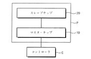
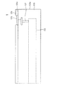
図1は、本発明の実施形態による半導体パッケージPの概念を説明する図である。
外部コントローラCが追加的に提供され得る。本発明の実施形態による半導体パッケージPはマスターチップ10及びスレーブチップ20を包含する。
マスターチップ10は外部コントローラCからアドレス及びコマンド等を含む制御信号、電圧信号、及び記録データ等を受信して、スレーブチップ20へ提供しスレーブチップ20を制御する。
FIG. 1 is a diagram illustrating the concept of a semiconductor package P according to an embodiment of the present invention.
An external controller C can additionally be provided. The semiconductor package P according to the embodiment of the present invention includes a
The
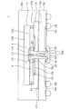
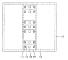
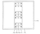
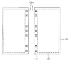
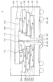
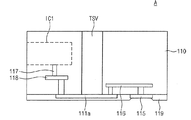
本発明の第1の実施形態による半導体パッケージ1を説明する。
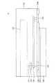
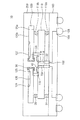
図2Aは本発明の第1の実施形態による半導体パッケージの断面図であり、図2B及び図2Cは各々図2Aの符号A及びB部の拡大図であり、図2Dは第1半導体チップ110の下部面を概略的に示す平面図であり、図2Eは第2半導体チップ120の上部面を概略的に示す平面図である。
A
2A is a cross-sectional view of the semiconductor package according to the first embodiment of the present invention, FIGS. 2B and 2C are enlarged views of portions A and B of FIG. 2A, respectively, and FIG. FIG. 2E is a plan view schematically showing an upper surface of the
図2A〜図2Eを参照すると、本発明の第1の実施形態による半導体パッケージ1は、パッケージ基板100、パッケージ基板100上の第1半導体チップ110、及びパッケージ基板100と第1半導体チップ110との間に実装され、互いに離隔された一対の第2半導体チップ120を含む。
2A to 2E, the
パッケージ基板100は、印刷回路基板であり得る。
パッケージ基板100は、その中央に開口部101を有する。パッケージ基板100は開口部101に隣接する回路パターン102を含む。回路パターン102はパッケージ基板100の下面に配置され、外部パッド104に電気的に接続される。半導体パッケージ1を外部装置と電気的に接続するソルダバンプ或いはソルダボールのような外部端子108が外部パッド104に付着される。
The
The
第1半導体チップ110は、パッケージ基板100と対向する第1面110a及び第1面に対向する第2面110bを有する。
第1半導体チップ110は、中央領域111及び中央領域両側の一対のセル領域112を包含する。
第1半導体チップ110は、第1集積回路IC1、第1センターパッド114及び第1ボンディングパッド115を包含する。
The
The
The
図2B及び図2Dに示すように、第1集積回路IC1は第1面110aに隣接する第1半導体チップ110の内部に形成される。
第1センターパッド114及び第1ボンディングパッド115は、中央領域111の第1面110aに配置される。
第1センターパッド114は、開口部101に露出される。第1ボンディングパッド115は第1センターパッド114と離隔されて配置される。第1ボンディングパッド115は第1コンタクト117及び第1内部パッド118を通じて第1集積回路IC1と電気的に接続される。
As shown in FIGS. 2B and 2D, the first integrated circuit IC1 is formed in the
The
The
一例として、第1ボンディングパッド115は、第1センターパッド114の両側に一対に配置される。
一対の第1ボンディングパッド115は、第1再配線116を通じて互いに接続される。
第1センターパッド114は、第1ボンディングパッド115及び第1再配線116とは分離される。
第1センターパッド114と第1ボンディングパッド115は第1集積回路IC1を通じて電気的に接続される。第1半導体チップ110の第1面110a上に第1センターパッド114及び第1ボンディングパッド115を露出する第1絶縁膜119が提供され得る。
As an example, the
The pair of
The
The
再び図2Aを参照すると、第2半導体チップ120は接着層210を通じてパッケージ基板100に付着される。
接着層210は、エポキシ或いはシリコン材質の絶縁性膜或いはテープであり得る。
第2半導体チップ120の互いに対向する縁端120eはパッケージ基板100の開口部101に隣接する。
第2半導体チップ120は、第1半導体チップ110の第1面110aと対向する第3面120a及び第3面に対向する第4面120bを有する。
Referring to FIG. 2A again, the
The
Edge edges 120 e of the
The
図2C及び図2Eに示すように、第2半導体チップ120は、第2集積回路IC2、第2センターパッド124及び第2ボンディングパッド125を包含する。
第2集積回路IC1は、第3面120aに隣接する第2半導体チップ120の内部に形成される。
第2センターパッド124及び第2ボンディングパッド125は、第2半導体チップ120の第3面120aに配置される。
第2センターパッド124は、第2半導体チップ120の中央領域121に配置される。第2センターパッド124の両側に一対のセル領域122が配置される。
As shown in FIGS. 2C and 2E, the
The second integrated circuit IC1 is formed inside the
The
The
第2ボンディングパッド125は、第2半導体チップ120の互いに対向する縁部120eに隣接して配置される。
第2ボンディングパッド125は、第1ボンディングパッド115に対応するように配置され、第2再配線126を通じて第2センターパッド124と電気的に接続される。
第2ボンディングパッド125は、第2再配線126、第2内部パッド128、及び第2コンタクト127を通じて第2集積回路IC2と電気的に接続される。
第2半導体チップ120の第3面120a上に第2ボンディングパッド125を露出する第2絶縁膜129が提供され得る。
The
The
The
A second insulating
再び図2Aを参照すると、半導体パッケージ1は、第1ボンディングパッド115と第2ボンディングパッド125とを電気的に接続する第1バンパー22、及び第1バンパー22と離隔して第1半導体チップ110と第2半導体チップ120とを支持するダミーバンパー24をさらに包含する。
第1バンパー22は、開口部101に隣接して第1半導体チップ110の下に配置され得る。ダミーバンパー24は、開口部101から離隔して第1半導体チップ110の下に配置される。
Referring to FIG. 2A again, the
The
メインボンディングワイヤ40が開口部101内に提供され、第1半導体チップ110の第1センターパッド114とパッケージ基板100の回路パターン102とを電気的に接続する。
モールディング層200が、第1半導体チップ110及び第2半導体チップ120を覆うように形成される。モールディング膜200は開口部101からパッケージ基板100の下に突出された突出部201を包含する。
A
The
第1半導体チップ110及び第2半導体チップ120は、DRAMやフラッシュのようなメモリチップであり得る。
第1半導体チップ110はマスターチップであって、第1集積回路IC1はデータを格納するためのメモリセル、メモリセルの動作を制御するための制御回路、及び/又は電源回路を包含することができる。
第2半導体チップ120はスレーブチップであって、第2集積回路IC2はデータを格納するためのメモリセルを包含することができる。第2半導体チップ120は制御回路及び/又は電源回路を包含しないことがあり得る。
The
The
The
第1半導体チップ110は、メインボンディングワイヤ40を通じて外部コントローラC(図1参照)と通信し、第1バンパー22を通じて第2半導体チップ120を制御することができる。
外部コントローラCからのアドレス及びコマンド信号等を含む制御信号、電圧信号、及び記録データ等はメインボンディングワイヤ40を通じて第1半導体チップ110に提供され、第1半導体チップ110又は第2半導体チップ120のメモリセルから読み出されたデータはメインボンディングワイヤ40を通じて外部コントローラCへ提供される。
The
A control signal including an address and a command signal from the external controller C, a voltage signal, and recording data are provided to the
第2半導体チップ120がメインボンディングワイヤ40及び第1半導体チップ110を通じて外部コントローラC(図1参照)と通信するので、通信での寄生キャパシタンスを減少させることができる。
これと共に、第1半導体チップ110及び第2半導体チップ120が貫通電極ではないボンディングワイヤを通じて、外部と接続されるので、半導体パッケージの製作費用が低減させることができる。
第1半導体チップ110及び第2半導体チップ120がメモリチップである場合、第1半導体チップ110は第2半導体チップ120各々の2倍のメモリ容量を有することができる。半導体パッケージ1の総メモリ容量は、第1半導体チップ110のメモリ容量の2n倍(nは整数)であり得る。
Since the
At the same time, since the
When the
次に、本発明の第2の実施形態による半導体パッケージ2を説明する。
図3Aは、本発明の第2の実施形態による半導体パッケージの断面図であり、図3B及び図3Cは各々図3Aの符号A及びB部の拡大図であり、図3Dは第1半導体チップ110の下部面を概略的に示す平面図であり、図3Eは第2半導体チップ120の上部面を概略的に示す平面図である。
図2A〜図2Eを参照して説明したことと重複する技術的な特徴に対する詳細な説明は省略し、相違点に対して詳細に説明する。
Next, a semiconductor package 2 according to a second embodiment of the present invention will be described.
3A is a cross-sectional view of a semiconductor package according to the second embodiment of the present invention, FIGS. 3B and 3C are enlarged views of portions A and B of FIG. 3A, respectively, and FIG. FIG. 3E is a plan view schematically showing an upper surface of the
Detailed descriptions of technical features that overlap with those described with reference to FIGS. 2A to 2E will be omitted, and differences will be described in detail.
図3A〜図3Eを参照すると、本発明の第2の実施形態による半導体パッケージ2で、第2半導体チップ120の第2集積回路IC2は、第2半導体チップ120の第1の実施形態の第2センターパッド124無しで、第2ボンディングパッド125に電気的に接続される。
言い換えれば、本発明の第1の実施形態による半導体パッケージ1と異なり、本発明の第2の実施形態による第2半導体チップ120の第2集積回路IC2は、第2半導体チップ120の縁部に隣接して配置されたエッジパッド、即ち第2ボンディングパッド125に直接電気的に接続される。
3A to 3E, in the semiconductor package 2 according to the second embodiment of the present invention, the second integrated circuit IC2 of the
In other words, unlike the
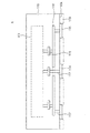
次に、本発明の第3の実施形態による半導体パッケージ3を説明する。
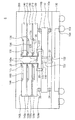
図4Aは本発明の第3の実施形態による半導体パッケージの断面図であり、図4Bは図4Aの符号A部分の拡大図である。
図2A〜図2Eを参照して説明したことと重複する技術的な特徴に対する詳細な説明は省略し、相違点に対して詳細に説明する。
Next, a
4A is a cross-sectional view of a semiconductor package according to the third embodiment of the present invention, and FIG. 4B is an enlarged view of a portion A in FIG. 4A.
Detailed descriptions of technical features that overlap with those described with reference to FIGS. 2A to 2E will be omitted, and differences will be described in detail.
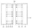
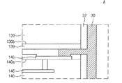
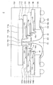
図4A及び図4Bを参照すると、本発明の第3の実施形態による半導体パッケージ3はパッケージ基板100、パッケージ基板100上の第1半導体チップ110、パッケージ基板100と第1半導体チップ110との間に実装され、互いに離隔された一対の第2半導体チップ120、パッケージ基板100と第2半導体チップ120との間に提供され、互いに離隔された一対の第3半導体チップ130、及びパッケージ基板100と第3半導体チップ130との間に提供され、互いに離隔された一対の第4半導体チップ140を包含する。
4A and 4B, the
第3半導体チップ130は、第2半導体チップ120と対向する第5面130a及び第5面に対向する第6面130bを有する。
第3半導体チップ130は、第3集積回路、第3センターパッド134、及び第3ボンディングパッド135を有する。第3半導体チップ130の第6面130b上に第3絶縁膜139が形成される。
第3集積回路は、図2Cに示した第2集積回路IC2のように、第5面130aに隣接する第3半導体チップ130の内部に配置される。第3センターパッド134及び第3ボンディングパッド135は第3半導体チップ120の第5面130aに配置される。
The
The
The third integrated circuit is arranged inside the
第3センターパッド134は、第3半導体チップ130の中央領域に配置される。
第3ボンディングパッド135は、第3半導体チップ130の互いに対向する縁端130eに隣接して配置される。第3ボンディングパッド135は第2ボンディングパッド125に対応するように配置され、第3再配線136を通じて第3センターパッド134と電気的に接続される。
これによって、第3ボンディングパッド135は第3センターパッド134を通じて第3集積回路と電気的に接続される(図2C参照)。
The
The
Accordingly, the
第4半導体チップ140の各々は、第3半導体チップ130と対向する第7面140a及び第7面に対向する第8面140bを有する。
第4半導体チップ140は、第4集積回路、第4センターパッド144、及び第4ボンディングパッド145を包含する。
第4集積回路は、図2Cに示した第2集積回路IC2のように、第7面140aに隣接する第4半導体チップ140の内部に配置される。
Each of the
The
The fourth integrated circuit is arranged inside the
第4センターパッド144及び第4ボンディングパッド145は、第4半導体チップ140の第7面140aに配置される。
第4センターパッド144は、第4半導体チップ140の中央領域に配置される。第4ボンディングパッド145は第4半導体チップ140の互いに対向する縁端140eに隣接して配置される。
第4ボンディングパッド145は、第3ボンディングパッド135に対応するように配置され、第4再配線146を通じて第4センターパッド144と電気的に接続される。
これによって、第4ボンディングパッド145は第4センターパッド144を通じて第4集積回路と電気的に接続される(図2C参照)。
The
The
The
Accordingly, the
第2半導体チップ120、第3半導体チップ130、第4半導体チップ140、及びパッケージ基板100は接着層210を通じて互いに付着される。
第2ボンディングパッド125、第3ボンディングパッド135、及び第4ボンディングパッド145はサイド接続方式で接続される。
例えば、図4Bに示すように、第2半導体チップ120、第3半導体チップ130、第4半導体チップ140の側壁に側壁絶縁膜32が形成され、側壁絶縁膜32上に金属配線30が形成される。
金属配線30は、第2半導体チップ120、第3半導体チップ130、及び第4半導体チップ140間を延長して第2ボンディングパッド125、第3ボンディングパッド135、及び第4ボンディングパッド145と接続される。金属配線30は、例えば銅(Cu)を包含することができる。
The
The
For example, as illustrated in FIG. 4B, the
The
次に、本発明の第4の実施形態による半導体パッケージ4を説明する。
図5は本発明の第4の実施形態による半導体パッケージの断面図である。
図4Aを参照して説明したことと重複する技術的な特徴に対する詳細な説明は省略し、相違点に対して詳細に説明する。
Next, a
FIG. 5 is a cross-sectional view of a semiconductor package according to the fourth embodiment of the present invention.
A detailed description of the technical features that overlap with those described with reference to FIG. 4A will be omitted, and the differences will be described in detail.
図5を参照すると、第3半導体チップ130は、第4半導体チップ140の第4ボンディングパッド145を露出するようにパッケージ基板100の縁端方向にシフトされる。第2半導体チップ120は第3半導体チップの第3ボンディングパッド135を露出するようにパッケージ基板100の縁端方向にシフトされる。
第1サブワイヤ42が開口部101内に提供されて、第2ボンディングパッド125と第3ボンディングパッド135とを電気的に接続する。
第2サブワイヤ44が開口部101内に提供されて、第3ボンディングパッド135と第4ボンディングパッド145とを電気的に接続する。
Referring to FIG. 5, the
A
A
次に、本発明の第5の実施形態による半導体パッケージ5を説明する。
図6Aは本発明の第5の実施形態による半導体パッケージの断面図であり、図6B及び図6Cは各々図6Aの符号A及びB部の拡大図である。
図2A〜図2Eを参照して説明したことと重複する技術的な特徴に対する詳細な説明は省略し、相違点に対して詳細に説明する。
Next, a
6A is a cross-sectional view of a semiconductor package according to a fifth embodiment of the present invention, and FIGS. 6B and 6C are enlarged views of portions A and B of FIG. 6A, respectively.
Detailed descriptions of technical features that overlap with those described with reference to FIGS. 2A to 2E will be omitted, and differences will be described in detail.
図6A〜図6Cを参照すると、第2半導体チップ120の第2集積回路IC2は第4面120bに隣接する第2半導体チップ120の内部に形成される。
第2センターパッド124及び第2ボンディングパッド125は第2半導体チップ120の第4面120bに配置される。
第2センターパッド124は、第2半導体チップ120の中央領域に配置される。
第2ボンディングパッド125は、第2半導体チップ120の互いに対向する縁部に隣接して配置される。
6A to 6C, the second integrated circuit IC2 of the
The
The
The
第2ボンディングパッド125は、第1ボンディングパッド115に対応するように配置され、第2再配線126を通じて第2センターパッド124に電気的に接続される。
第2センターパッド124は、第2内部パッド128と第2コンタクト127を通じて第2集積回路IC2に電気的に接続される。
第2半導体チップ120の第4面120b上に第2ボンディングパッド125を露出する第2絶縁膜129が提供され得る。
The
The
A second insulating
パッケージ基板100、第1半導体チップ110、及び第2半導体チップ120は、接着層210を通じて互いに付着される。接着層210は、エポキシ或いはシリコン材質の絶縁性膜或いはテープであり得る。
第2半導体チップ120は、第2半導体チップの第2ボンディングパッド125を露出するように開口部101に向かってシフトされる。
第2半導体チップ120は第1ボンディングパッド115を露出させる。
第1サブワイヤ42が開口部101内に提供されて、第1ボンディングパッド115と第2ボンディングパッド125とを電気的に接続する。
The
The
The
A
次に、本発明の第6の実施形態による半導体パッケージ6を説明する。
図7は本発明の第6の実施形態による半導体パッケージの断面図である。
図6A〜図6Cを参照して説明したことと重複する技術的な特徴に対する詳細な説明は省略し、相違点に対して詳細に説明する。
Next, a
FIG. 7 is a sectional view of a semiconductor package according to a sixth embodiment of the present invention.
Detailed descriptions of technical features that overlap with those described with reference to FIGS. 6A to 6C will be omitted, and differences will be described in detail.
図7を参照すると、本発明の第6の実施形態による半導体パッケージ6は、パッケージ基板100と第2半導体チップ120との間に提供され、互いに離隔された一対の第3半導体チップ130、及びパッケージ基板100と第3半導体チップ130との間に提供され、互いに離隔された一対の第4半導体チップ140を包含する。
第3半導体チップ130は第3集積回路、第3センターパッド134、及び第3ボンディングパッド135を包含する。第3半導体チップ130は第2半導体チップ120と対向する第5面130a及び第5面に対向する第6面130bを有する。
Referring to FIG. 7, a
The
第3集積回路は、図6Cに示した第2集積回路IC2のように、第6面130bに隣接する第3半導体チップ130の内部に形成される。
第3センターパッド134及び第3ボンディングパッド135は第3半導体チップ130の第6面130bに配置される。
第3センターパッド134は、第3半導体チップ130の中央領域に配置され得る。第3ボンディングパッド135は第3半導体チップ130の互いに対向する縁端130eに隣接して配置される。第3ボンディングパッド135は第2ボンディングパッド125に対応するように配置され、第3再配線136を通じて第3センターパッド134と電気的に接続される。
これによって、第3ボンディングパッド135は第3センターパッド134を通じて第3集積回路と電気的に接続される。
The third integrated circuit is formed inside the
The
The
Accordingly, the
第4半導体チップ140は、第4集積回路、第3センターパッド144、及び第4ボンディングパッド145を含む。
第4半導体チップ140は、第3半導体チップ130と対向する第7面140a及び第7面に対向する第8面140bを有する。
第4集積回路は、図6Cに示した第2集積回路IC2のように、第8面140bに隣接する第4半導体チップ140の内部に形成される。
第4センターパッド144及び第4ボンディングパッド145は第4半導体チップ140の第8面140bに配置される。
The
The
The fourth integrated circuit is formed inside the
The
第4センターパッド144は、第4半導体チップ140の中央領域に配置される。
第4ボンディングパッド145は、第4半導体チップ140の互いに対向する縁部に隣接して配置される。
第4ボンディングパッド145は第3ボンディングパッド135に対応するように配置され、第4再配線146を通じて第4センターパッド144に電気的に接続される。
これによって、第4ボンディングパッド145は第4センターパッド144を通じて第4集積回路と電気的に接続される。
The
The
The
Accordingly, the
第3半導体チップ130は、第3半導体チップの第3ボンディングパッド135を露出するように開口部101に向かってシフトされる。
第4半導体チップ140は、第4半導体チップの第4ボンディングパッド145を露出するように開口部101に向かってシフトされる。
第2サブワイヤ44が開口部101内に提供されて、第2ボンディングパッド125と第3ボンディングパッド135とを電気的に接続する。
第3サブワイヤ46が開口部101内に提供されて、第3ボンディングパッド135と第4ボンディングパッド145とを電気的に接続する。
The
The
A
A
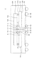
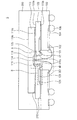
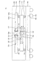
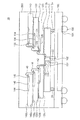
本発明の第7の実施形態による半導体パッケージ7Aを説明する。
図8Aは本発明の第7の実施形態による半導体パッケージの断面図であり、図8Bは図8Aの符号A部の拡大図である。
図8A及び図8Bを参照すると、半導体パッケージ7Aは、回路パターンを有するパッケージ基板100、パッケージ基板上の第1半導体チップ110、及び第1半導体チップ上に互いに離隔した一対の第2半導体チップ120を含む。
A
FIG. 8A is a cross-sectional view of a semiconductor package according to a seventh embodiment of the present invention, and FIG. 8B is an enlarged view of a portion A in FIG. 8A.
Referring to FIGS. 8A and 8B, a
パッケージ基板100は印刷回路基板であり得る。
パッケージ基板100は回路パターン102を含む。回路パターン102はパッケージ基板100の下面に配置された外部パッド104と電気的に接続される。
半導体パッケージ6と外部装置とを電気的に接続できるソルダバンプ或いはソルダボールのような外部端子108が外部パッド104に付着される。
The
第1半導体チップ110は、パッケージ基板100と対向する第1面110a及び第1面に対向する第2面110bを有する。
第1半導体チップ110は、第1集積回路IC1、貫通電極(through−silicon via)TSV、及び第1ボンディングパッド115を包含する。
第1集積回路IC1は、第2面110bに隣接する第1半導体チップ110の内部に形成される。
貫通電極TSVは、第1半導体チップ110の中央領域に配置される。
貫通電極TSVは、第1半導体チップ110の基板を貫通して形成され、第1半導体チップ110の第1面110aの下部パッド111aと第2面110bの上部パッド111bとを接続する。
The
The
The first integrated circuit IC1 is formed inside the
The through electrode TSV is disposed in the central region of the
The through electrode TSV is formed to penetrate the substrate of the
第1ボンディングパッド115は、貫通電極TSVと離隔して、第1半導体チップ110の中央領域に配置される。
第1ボンディングパッド115は、第1半導体チップ110の第2面110bに配置される。第1ボンディングパッド115は第1コンタクト117及び第1内部パッド118を通じて第1集積回路IC1に電気的に接続される。
第1ボンディングパッド115は、貫通電極TSVの両側に一対に配置される。第1ボンディングパッド115は、第1再配線116を通じて貫通電極TSVと電気的に接続される。第1半導体チップ110の第2面110b上に第1ボンディングパッド115を露出する第1絶縁膜119が提供され得る。
The
The
The
第1半導体チップ110とパッケージ基板100との間に第1バンパー22が提供されて、貫通電極TSVと回路パターン102とを電気的に接続する。
半導体パッケージ6は、第1バンパー22と離隔して、第1半導体チップ110とパッケージ基板100を支持する第1ダミーバンパー24をさらに包含することができる。
A
The
一対の第2半導体チップ120は、第1半導体チップ110の中央領域を露出するように互いに離隔される。
第2半導体チップ120の互いに対向する縁端120eは第1半導体チップ110の中央領域に隣接する。
第2半導体チップ120は、第1半導体チップ110と対向する第3面120a及び第3面に対向する第4面120bを有する。
第2半導体チップ120の各々は、第2集積回路、第2センターパッド124、及び第2ボンディングパッド125を包含する。
The pair of
Edge edges 120 e of the
The
Each of the
第2集積回路は、図2Cに示したように、第4面120bに隣接する第2半導体チップ120の内部に形成される。
第2センターパッド124は、第2半導体チップ120の中央領域に配置される。
第2ボンディングパッド125は、第2半導体チップ120の互いに対向する縁端120eに隣接して配置される。
第2センターパッド124及び第2ボンディングパッド125は第2半導体チップ120の第4面120bに配置される。
第2ボンディングパッド125は第2再配線126を通じて第2センターパッド124と電気的に接続される。第2センターパッド124は第2集積回路IC2と電気的に接続される。
これによって、第2ボンディングパッド125は第2センターパッド124を通じて第2集積回路IC2と電気的に接続される。
As shown in FIG. 2C, the second integrated circuit is formed in the
The
The
The
The
Accordingly, the
第2半導体チップ120の第3面120aに接続パッド127が提供される。
接続パッド127は、第2ボンディングパッド125と対応するように提供される。第2半導体チップ120の第3面120a上に接続パッド127を露出する第2絶縁膜129が提供され得る。
第2ボンディングパッド125と連結パッド127とはサイド接続方式で接続される。
例えば、図8Bに示すように、第2半導体チップ120の側壁に側壁絶縁膜32が形成され、側壁絶縁膜32上に金属配線30が形成される。
金属配線30は、第2半導体チップ120の第3面120a及び第4面120bに延長して第2ボンディングパッド125と接続パッド127とを接続する。金属配線30は、例えば銅(Cu)を包含することができる。
The
The
For example, as shown in FIG. 8B, the
The
第1半導体チップ110と第2半導体チップ120との間に第2バンパー26が提供されて、接続パッド127と第1ボンディングパッド115とを接続することができる。
半導体パッケージ6は、第2バンパー26と離隔して第1半導体チップ110と第2半導体チップ120とを支持する第2ダミーバンパー28をさらに包含することができる。
A
The
次に、本発明の第7の実施形態の変形にしたがう半導体パッケージ7Bを説明する。
図9は、本発明の第7の実施形態の変形にしたがう半導体パッケージの断面図である。
図8A及び図8Bを参照して説明したことと重複する技術的な特徴に対する詳細な説明は省略し、相違点に対して詳細に説明する。
Next, a
FIG. 9 is a cross-sectional view of a semiconductor package according to a modification of the seventh embodiment of the present invention.
Detailed descriptions of technical features that overlap with those described with reference to FIGS. 8A and 8B will be omitted, and differences will be described in detail.
図9を参照すると、本発明の第7の実施形態による半導体パッケージ7Aとは異なり、本発明の第7の実施形態の変形にしたがう半導体パッケージ7Bの第1ボンディングパッド115は、第1再配線116ではないボンディングワイヤ40を通じて貫通電極TSVと電気的に接続される。
Referring to FIG. 9, unlike the
次に、本発明の第8の実施形態による半導体パッケージ8を説明する。
図10は、本発明の第8の実施形態による半導体パッケージの断面図である。
図8A及び図8Bを参照して説明したことと重複する技術的な特徴に対する詳細な説明は省略し、相違点に対して詳細に説明する。
Next, a
FIG. 10 is a cross-sectional view of a semiconductor package according to the eighth embodiment of the present invention.
Detailed descriptions of technical features that overlap with those described with reference to FIGS. 8A and 8B will be omitted, and differences will be described in detail.
図10を参照すると、本発明の第8の実施形態による半導体パッケージ8は、パッケージ基板100、パッケージ基板100上の第1半導体チップ110、第1半導体チップ110上に実装され互いに離隔された一対の第2半導体チップ120、第2半導体チップ120上に提供され互いに離隔された一対の第3半導体チップ130、及び第3半導体チップ130上に提供され互いに離隔された一対の第4半導体チップ140を包含する。
第3半導体チップ130の各々は、第3集積回路、第3センターパッド134、及び第3ボンディングパッド135を包含する。第3半導体チップ130の各々は第2半導体チップ120と対向する第5面130a及び第5面に対向する第6面130bを有する。
Referring to FIG. 10, a
Each of the
第3集積回路は、図2Cに示した第2集積回路IC2のように、第6面130bに隣接する第3半導体チップ130の内部に配置される。
第3センターパッド134及び第3ボンディングパッド135は第3半導体チップ120の第6面130bに配置される。
第3センターパッド134は、第3半導体チップ130の中央領域に配置される。
第3ボンディングパッド135は、第3半導体チップ130の互いに対向する縁端130eに隣接して配置される。
第3ボンディングパッド135は第2ボンディングパッド125に対応するように配置され、第3再配線136を通じて第3センターパッド134と電気的に接続される。
これによって、第3ボンディングパッド135は第3センターパッド134を通じて第3集積回路と電気的に接続される。
The third integrated circuit is disposed inside the
The
The
The
The
Accordingly, the
第4半導体チップ140の各々は第4集積回路、第4センターパッド144及び第4ボンディングパッド145を包含する。
第4半導体チップ140の各々は、第3半導体チップ130と対向する第7面140a及び第7面に対向する第8面140bを有する。
第4集積回路は、図2Cに示した第2集積回路IC2のように、第8面140bに隣接する第4半導体チップ140の内部に配置される。
第4センターパッド144及び第4ボンディングパッド145は第4半導体チップ140の第8面140bに配置される。
Each of the
Each of the
The fourth integrated circuit is arranged inside the
The
第4センターパッド144は、第4半導体チップ140の中央領域に配置される。
第4ボンディングパッド145は、第4半導体チップ140の互いに対向する縁端140eに隣接して配置される。
第4ボンディングパッド145は、第3ボンディングパッド135に対応するように配置され、第4再配線146を通じて第4センターパッド144と電気的に接続される。
これによって、第4ボンディングパッド145は第4センターパッド144を通じて第4集積回路と電気的に接続される(図2C参照)。
第2半導体チップ120、第3半導体チップ130、及び第4半導体チップ140は接着層210を通じて互いに付着される。
The
The
The
Accordingly, the
The
接続パッド127、第2ボンディングパッド125、第3ボンディングパッド135、及び第4ボンディングパッド145はサイド接続方式で接続される。
例えば、図8Bのように、第2半導体チップ120、第3半導体チップ130、第4半導体チップ140の側壁に側壁絶縁膜32が形成され、側壁絶縁膜32上に金属配線30が形成される。
金属配線30は、接続パッド127、第2ボンディングパッド125、第3ボンディングパッド135、及び第4ボンディングパッド145と接続される。
金属配線30は、例えば銅(Cu)を包含することができる。
The
For example, as shown in FIG. 8B, the
The
The
次に、本発明の第9の実施形態による半導体パッケージ9を説明する。
図11は、本発明の第9の実施形態による半導体パッケージの断面図である。
図10を参照して説明したことと重複する技術的な特徴に対する詳細な説明は省略し、相違点に対して詳細に説明する。
Next, a
FIG. 11 is a cross-sectional view of a semiconductor package according to the ninth embodiment of the present invention.
A detailed description of the technical features that overlap with those described with reference to FIG. 10 will be omitted, and the differences will be described in detail.
図11を参照すると、第3半導体チップ130は、第2半導体チップ120の第2ボンディングパッド125を露出するように、第2半導体チップ120に比べてパッケージ基板100の外側の縁部方向にシフトされる。
第4半導体チップ140は、第3半導体チップ130の第3ボンディングパッド135を露出するように、第3半導体チップ130に比べてパッケージ基板100の外側の縁部方向にシフトされる。
接続パッド127、第2ボンディングパッド125、第3ボンディングパッド135、及び第4ボンディングパッド145は、サイド接続方式で接続される。
第2半導体チップ120は、バンパー26を通じて第1半導体パッケージ110に接続される。
Referring to FIG. 11, the
The
The
The
次に、本発明の第10の実施形態による半導体パッケージ10を説明する。
図12は、本発明の第10の実施形態による半導体パッケージの断面図である。
図11を参照して説明したことと重複する技術的な特徴に対する詳細な説明は省略し、相違点に対して詳細に説明する。
Next, a
FIG. 12 is a sectional view of a semiconductor package according to the tenth embodiment of the present invention.
A detailed description of the technical features that overlap with those described with reference to FIG. 11 will be omitted, and the differences will be described in detail.
図12を参照すると、第2半導体チップ120は接着層210を通じて第1半導体パッケージ110に付着される。
第3半導体チップ130は、第2半導体チップ120の第2ボンディングパッド125を露出するようにパッケージ基板100の外側の縁部方向にシフトされ、第4半導体チップ140は第3半導体チップ130の第3ボンディングパッド135を露出するようにパッケージ基板100の外側の縁部方向にシフトされる。
Referring to FIG. 12, the
The
第1ボンディングパッド115と第2ボンディングパッド125とは第1サブワイヤ42を通じて、第2ボンディングパッド125と第3ボンディングパッド135とは第2サブワイヤ44を通じて、第3ボンディングパッド135と第4ボンディングパッド145は第3サブワイヤ46を通じて電気的に接続される。
又、上述した第7〜第10の実施形態の第1ボンディングパッド115は、変形例として、第1再配線ではない図9を参照して説明したようにメインボンディングワイヤ40を通じて貫通電極TSVと電気的に接続させることもできる。
The
Further, as a modification, the
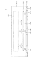
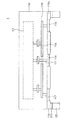
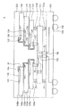
次に、本発明の第11の実施形態による半導体パッケージ11を説明する。
図13Aは本発明の第11の実施形態による半導体パッケージの断面図であり、図13B及び図13Cは各々図13Aの符号A及びB部の拡大図である。
図13A〜図13Cを参照すると、半導体パッケージ10は、回路パターン102を有するパッケージ基板100、パッケージ基板上の第1半導体チップ110、及び第1半導体チップ上に互いに離隔された一対の第2半導体チップ120を含む。
Next, a
FIG. 13A is a cross-sectional view of a semiconductor package according to an eleventh embodiment of the present invention, and FIGS. 13B and 13C are enlarged views of portions A and B of FIG. 13A, respectively.
13A to 13C, a
パッケージ基板100は印刷回路基板であり得る。
パッケージ基板100は回路パターン102を含む。回路パターン102はパッケージ基板100の下面に配置された外部パッド104と電気的に接続される。
半導体パッケージ11を外部装置に電気的に接続させるソルダバンプ或いはソルダボールのような1つ或いはそれ以上の外部端子108が外部パッド104に付着される。
The
One or more
第1半導体チップ110は、パッケージ基板100と対向する第1面110a及び第1面に対向する第2面110bを有する。
第1半導体チップ110は、第1集積回路IC1、貫通電極TSV、及び第1ボンディングパッド115を包含する。
第1集積回路IC1は、第1面110aに隣接する第1半導体チップ110の内部に形成される。
貫通電極TSVは、第1半導体チップ110の中央領域に配置される。
貫通電極TSVは、第1半導体チップ110の基板を貫通して形成され、第1半導体チップ110の第1面110aの下部パッド111aと第2面110bの上部パッド111bとを接続させる。
The
The
The first integrated circuit IC1 is formed inside the
The through electrode TSV is disposed in the central region of the
The through electrode TSV is formed to penetrate the substrate of the
第1ボンディングパッド115は、貫通電極TSVと離隔されて第1半導体チップ110の中央領域に配置される。
第1ボンディングパッド115は、第1半導体チップ110の第1面110aに配置される。
第1ボンディングパッド115は貫通電極TSVに隣接して配置される。第1ボンディングパッド115は第1再配線116を通じて貫通電極TSVに電気的に接続される。第1ボンディングパッド115は、下部パッド111a、第1コンタクト117及び第1内部パッド118を通じて第1集積回路IC1と電気的に接続される。
The
The
The
第1半導体チップ110とパッケージ基板100との間に第1バンパー22が提供されて、第1ボンディングパッド115と回路パターン102とを電気的に接続する。
第1半導体チップ110とパッケージ基板100との間に第1バンパー22と離隔した第1ダミーバンパー24が追加的に提供され得る。
第1半導体チップ110の第1面110aに第1絶縁膜119が提供されて、第1ボンディングパッド115を露出する。
A
A
A first insulating
一対の第2半導体チップ120は、第1半導体チップ110の中央領域を露出するように互いに離隔される。
第2半導体チップ120の互いに対向する縁端は、第1半導体チップ110の中央領域に隣接することができる。
第2半導体チップ120の各々は、第1半導体チップ110と対向する第3面120a及び第3面に対向する第4面120bを有する。
第2半導体チップ120の各々は、第2集積回路IC2、第2センターパッド124及び第2ボンディングパッド125を包含する。
The pair of
The opposing edges of the
Each of the
Each of the
第2集積回路IC2は、第3面120aに隣接する第2半導体チップ120の内部に形成される。
第2センターパッド114は、第2半導体チップ120の中央領域に配置される。
第2ボンディングパッド125は、第2半導体チップ120の互いに対向する縁端120eに隣接して配置される。
第2センターパッド124及び第2ボンディングパッド125は第2半導体チップ120の第3面120aに配置される。
第2ボンディングパッド125は、第2再配線126を通じて第2センターパッド124に電気的に接続される。
第2センターパッド124は、第2コンタクト127及び第2内部パッド128を通じて第2集積回路IC2に電気的に接続される。
第2半導体チップ120の第3面120a上に第2ボンディングパッド125を露出する第2絶縁膜129が提供され得る。
The second integrated circuit IC2 is formed inside the
The
The
The
The
The
A second insulating
第1半導体チップ110と第2半導体チップ120との間に第2バンパー26が提供されて、第2ボンディングパッド125と上部パッド111bを接続する。
第1半導体チップ110と第2半導体チップ120との間に第2バンパー26と離隔した第2ダミーバンパー28が追加的に提供され得る。
A
A
次に、本発明の第12の実施形態による半導体パッケージ12を説明する。
図14は本発明の第12の実施形態による半導体パッケージの断面図である。
図13A〜図13Cを参照して説明したことと重複する技術的な特徴に対する詳細な説明は省略し、相違点に対して詳細に説明する。
Next, a
FIG. 14 is a sectional view of a semiconductor package according to a twelfth embodiment of the present invention.
Detailed descriptions of technical features that overlap with those described with reference to FIGS. 13A to 13C will be omitted, and differences will be described in detail.
図14を参照して、本発明の第12の実施形態による半導体パッケージ12は、パッケージ基板100、パッケージ基板100上の第1半導体チップ110、第1半導体チップ110上に実装され互いに離隔された一対の第2半導体チップ120、第2半導体チップ120上に提供され互いに離隔された一対の第3半導体チップ130、及び第3半導体チップ130上に提供され互いに離隔された一対の第4半導体チップ140を包含する。
Referring to FIG. 14, a
第3半導体チップ130の各々は、第3集積回路、第3センターパッド134、及び第3ボンディングパッド135を有する。
第3ボンディングパッド135は、第3集積回路と電気的に接続される。
第3半導体チップ130の各々は、第2半導体チップ120と対向する第5面130a及び第5面に対向する第6面130bを有する。
第3集積回路は、図13Cに示した第2集積回路IC2のように、第5面130aに隣接する第3半導体チップ130の内部に配置される。
Each of the
The
Each of the
The third integrated circuit is arranged inside the
第3センターパッド134及び第3ボンディングパッド135は、第3半導体チップ120の第5面130aに配置される。
第3センターパッド134は、第3半導体チップ130の中央領域に配置される。
第3ボンディングパッド135は、第3半導体チップ130の互いに対向する縁端130eに隣接して配置される。
第3ボンディングパッド135は第2ボンディングパッド125に対応するように配置され、第3再配線136を通じて第3センターパッド134と電気的に接続される。
これによって、第3ボンディングパッド135は、第3センターパッド134を通じて第3集積回路と電気的に接続される。
The
The
The
The
Accordingly, the
第4半導体チップ140の各々は、第4集積回路、第4センターパッド144及び互いに対向するそれらの縁部に配置される第4ボンディングパッド145を包含する。
第4半導体チップ140の各々は、第3半導体チップ130と対向する第7面140a及び第7面に対向する第8面140bを有する。
第4集積回路は、図13Cに示した第2集積回路IC2のように、第7面140aに隣接する第4半導体チップ140の内部に配置される。
Each of the
Each of the
The fourth integrated circuit is arranged inside the
第4センターパッド144及び第4ボンディングパッド145は、第4半導体チップ140の第7面140aに配置される。
第4センターパッド144は、第4半導体チップ140の中央領域に配置される。
第4ボンディングパッド145は、第4半導体チップ140の互いに対向する縁端140eに隣接して配置される。
第4ボンディングパッド145は、第3ボンディングパッド135に対応するように配置され、第4再配線146を通じて第4センターパッド144と電気的に接続される。
これによって、第4ボンディングパッド145は、第4センターパッド144を通じて第4集積回路と電気的に接続される。
The
The
The
The
Accordingly, the
第2半導体チップ120、第3半導体チップ130、及び第4半導体チップ140は接着層210を通じて互いに付着される。
第2ボンディングパッド125、第3ボンディングパッド135、及び第4ボンディングパッド145は、図10で示したように、サイド接続方式で接続される。
The
As shown in FIG. 10, the
次に、本発明の第13の実施形態による半導体パッケージ13を説明する。
図15は、本発明の第13の実施形態による半導体パッケージの断面図である。
図14を参照して説明したことと重複する技術的な特徴に対する詳細な説明は省略し、相違点に対して詳細に説明する。
Next, a
FIG. 15 is a cross-sectional view of a semiconductor package according to a thirteenth embodiment of the present invention.
A detailed description of the technical features that overlap with those described with reference to FIG. 14 will be omitted, and the differences will be described in detail.
図15を参照すると、第3半導体チップ130は、第3半導体チップ130の第3ボンディングパッド135を露出するようにパッケージ基板100の中央方向にシフトされ、第4半導体チップ140は、第4半導体チップ140の第4ボンディングパッド145を露出するようにパッケージ基板100の中央方向にシフトされる。
第2ボンディングパッド125と第3ボンディングパッド135とは第1サブワイヤ42を通じて、第3ボンディングパッド135と第4ボンディングパッド145とは第2サブワイヤ44を通じて接続される。
Referring to FIG. 15, the
The
上述した第11〜第13の実施形態では、第1半導体チップ110の第1集積回路IC1は第1面110aに隣接する第1半導体チップ110の内部に形成され、第1ボンディングパッド115は第1半導体チップ110の第1面110aに配置されることとして説明した。
しかし、これに限定されない。図8A及び図8Bを参照して説明したように、第1半導体チップ110の第1集積回路IC1は第2面110bに隣接する第1半導体チップ110の内部に形成し、第1ボンディングパッド115は第1半導体チップ110の第2面110bに配置することも可能である。
In the above-described first to thirteenth embodiments, the first integrated circuit IC1 of the
However, it is not limited to this. As described with reference to FIGS. 8A and 8B, the first integrated circuit IC1 of the
上述した第3〜第13の実施形態では、ボンディングパッドがセンターパッドと接続されたものを説明したが、これに限定されない。
例えば、図3A〜図3Eを参照して説明した第2の実施形態のように、集積回路をセンターパッド無しで半導体チップの縁部に隣接して配置されたエッジパッド、即ちボンディングパッドに直接接続させることもできる。
In the third to thirteenth embodiments described above, the bonding pad is connected to the center pad, but the present invention is not limited to this.
For example, as in the second embodiment described with reference to FIGS. 3A to 3E, the integrated circuit is directly connected to an edge pad, that is, a bonding pad arranged adjacent to the edge of the semiconductor chip without a center pad. It can also be made.
上述した第4、第5、第6、第10及び第13の実施形態は、サブワイヤを使用するワイヤボンディングでボンディングパッドを接続することを説明したが、これに限定されない。
例えば、図11を参照して説明したサイド接続方式で接続することも可能である。
In the fourth, fifth, sixth, tenth and thirteenth embodiments described above, the bonding pads are connected by wire bonding using a sub-wire. However, the present invention is not limited to this.
For example, it is possible to connect by the side connection method described with reference to FIG.
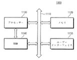
図16は、本発明の実施形態による電子システム1000を示すブロック図である。
図16を参照すると、電子システム1000は、本発明の実施形態による半導体パッケージを少なくとも1つ包含する。
電子システム1000は、モバイル機器やコンピューター等を包含することができる。
FIG. 16 is a block diagram illustrating an
Referring to FIG. 16, the
The
例えば、電子システム1000は、メモリシステム1120、プロセッサー1130、RAM1140、及びユーザーインターフェイス1150を包含でき、これらはバス(Bus)1110を利用して互いにデータ通信を行う。
プロセッサー1130は、プログラムを実行し、電子システム700を制御する役割を果たす。
RAM1140は、プロセッサー1130の動作メモリとして使用される。
例えば、メモリシステム1120、プロセッサー1130、及びRAM1140は、本発明の実施形態による半導体パッケージを包含することができる。
For example, the
The
The
For example, the
又は、プロセッサー1130とRAM1140とを1つのパッケージに包含することもできる。
ユーザーインターフェイス1150は、電子システム1000にデータを入力又は出力するのに利用される。
メモリシステム1120は、プロセッサー1130の動作のためのコード、プロセッサー1130によって処理されたデータ、又は外部から入力されたデータを格納することができる。
Alternatively, the
The
The
図16の電子システムは、多様な電子機器の電子制御装置に適用され得る。
図16の電子システムは、例えばスマートフォンのようなモバイル機器、コンピューター、MP3プレーヤー、ナビゲーション(Navigation)、ソリッドステートドライブ(Solid State Drive;SSD)、サーバー、自動車又は家電製品(Household appliances)に適用され得る。
The electronic system of FIG. 16 can be applied to electronic control apparatuses of various electronic devices.
The electronic system shown in FIG. 16 can be applied to, for example, a mobile device such as a smartphone, a computer, an MP3 player, navigation, a solid state drive (SSD), a server, an automobile, or a homehold appliance. .
尚、本発明は、上述の実施形態に限られるものではない。本発明の技術的範囲から逸脱しない範囲内で多様に変更実施することが可能である。 The present invention is not limited to the embodiment described above. Various modifications can be made without departing from the technical scope of the present invention.
1、P 半導体パッケージ
10 マスターチップ
20 スレーブチップ
22 第1バンパー
24 ダミーバンパー
100 パッケージ基板
101 開口部
102 回路パターン
104 外部パッド
108 外部端子
110 第1半導体チップ
111、121 中央領域
112、122 セル領域
114 第1センターパッド
115 第1ボンディングパッド
116 第1再配線
117、127 (第1、第2)コンタクト
118、128 (第1、第2)内部パッド
119、129 (第1、第2)絶縁膜
120 第2半導体チップ
120e 縁端
124 第2センターパッド
125 第2ボンディングパッド
126 第2再配線
200 モールディング層
201 突出部
210 接着層
C コントローラ
DESCRIPTION OF
Claims (34)
パッケージ基板と、
前記パッケージ基板上に配置される第1半導体チップと、
前記パッケージ基板と前記第1半導体チップとの間に搭載される一対の第2半導体チップと、
接続部材とを有し、
前記パッケージ基板は、その中央領域に配置された開口部と、前記開口部に隣接して配置された回路パターンとを含み、
前記第1半導体チップは、第1集積回路と、
その中央領域に前記開口部と整列配置され第1ワイヤを通じて前記回路パターンと電気的に接続される第1センターパッドと、
前記第1半導体チップの中央領域に配置され前記第1センターパッドと離隔して前記第1集積回路と電気的に接続される複数の第1ボンディングパッドとを含み、
前記第2半導体チップは、前記開口部の対向する両側に離隔して配置され、
第2集積回路と、
前記第2集積回路の対向する縁部に隣接し前記第1ボンディングパッドと対応するように配置され、前記第2集積回路と電気的に接続される複数の第2ボンディングパッドとを含み、
前記接続部材は、前記第1ボンディングパッドと前記第2ボンディングパッドとを電気的に接続し、
前記第1半導体チップは、前記各々の第2半導体チップの2倍のメモリ容量を有し、前記半導体パッケージの総メモリ容量は、前記第1半導体チップのメモリ容量の2n倍(nは整数)であることを特徴とする半導体パッケージ。 A semiconductor package,
A package substrate;
A first semiconductor chip disposed on the package substrate;
A pair of second semiconductor chips mounted between the package substrate and the first semiconductor chip;
A connecting member,
The package substrate includes an opening disposed in a central region thereof, and a circuit pattern disposed adjacent to the opening.
The first semiconductor chip includes a first integrated circuit;
A first center pad arranged in alignment with the opening in the central region and electrically connected to the circuit pattern through a first wire;
A plurality of first bonding pads disposed in a central region of the first semiconductor chip and spaced apart from the first center pad and electrically connected to the first integrated circuit;
The second semiconductor chip is spaced apart on opposite sides of the opening,
A second integrated circuit;
A plurality of second bonding pads disposed adjacent to opposing edges of the second integrated circuit and corresponding to the first bonding pads and electrically connected to the second integrated circuit;
The connection member electrically connects the first bonding pad and the second bonding pad;
The first semiconductor chip has a memory capacity twice that of each of the second semiconductor chips, and the total memory capacity of the semiconductor package is 2 n times (n is an integer) the memory capacity of the first semiconductor chip. A semiconductor package characterized by the above.
前記第2半導体チップの各々は、前記第1半導体チップの前記第1面と対向する第3面及び前記第3面と対向する第4面を有し、前記第2ボンディングパッドは、前記第3面に配置されることを特徴とする請求項1に記載の半導体パッケージ。 The first semiconductor chip has a first surface facing the package substrate and a second surface facing the first surface, and the first center pad and the first bonding pad are disposed on the first surface. ,
Each of the second semiconductor chips has a third surface facing the first surface of the first semiconductor chip and a fourth surface facing the third surface, and the second bonding pad is the third surface. The semiconductor package according to claim 1, wherein the semiconductor package is disposed on a surface.
前記パッケージ基板と前記第3半導体チップとの間に、前記開口部の対向する両側に離隔して配置される一対の第4半導体チップとを更に有し、
前記第3半導体チップは、第3集積回路と、
前記開口部と隣接して前記第3半導体チップの互いに対向する縁部に配置され、前記第3集積回路と電気的に接続される第3ボンディングパッドとを含み、
前記第4半導体チップは、第4集積回路と、
前記開口部と隣接して前記第4半導体チップの互いに対向する縁部に配置され、前記第4集積回路と電気的に接続される第4ボンディングパッドとを含み、
前記第2ボンディングパッド、前記第3ボンディングパッド、及び前記第4ボンディングパッドは、サイド接続方式又はワイヤ接続方式で接続されることを特徴とする請求項3に記載の半導体パッケージ。 A pair of third semiconductor chips disposed between the package substrate and the second semiconductor chip and spaced apart on opposite sides of the opening;
A pair of fourth semiconductor chips disposed between the package substrate and the third semiconductor chip and spaced apart on opposite sides of the opening;
The third semiconductor chip includes a third integrated circuit,
A third bonding pad disposed adjacent to the opening and adjacent to the third semiconductor chip and electrically connected to the third integrated circuit;
The fourth semiconductor chip includes a fourth integrated circuit,
A fourth bonding pad disposed adjacent to the opening and adjacent to the fourth semiconductor chip and electrically connected to the fourth integrated circuit;
4. The semiconductor package according to claim 3, wherein the second bonding pad, the third bonding pad, and the fourth bonding pad are connected by a side connection method or a wire connection method.
前記第4半導体チップの各々は、前記第3半導体チップの前記第6面と対向する第7面及び前記第7面と対向する第8面を有し、前記第4ボンディングパッドは、前記第7面に配置されることを特徴とする請求項6に記載の半導体パッケージ。 Each of the third semiconductor chips has a fifth surface facing the second semiconductor chip and a sixth surface facing the fifth surface, and the third bonding pad is disposed on the fifth surface,
Each of the fourth semiconductor chips has a seventh surface that faces the sixth surface of the third semiconductor chip and an eighth surface that faces the seventh surface, and the fourth bonding pad has the seventh surface. The semiconductor package according to claim 6, wherein the semiconductor package is disposed on a surface.
前記第2半導体チップの各々は、前記第1半導体チップの前記第1面と対向する第3面及び前記第3面と対向する第4面を有し、前記第2ボンディングパッドは、前記第4面に配置されることを特徴とする請求項1に記載の半導体パッケージ。 The first semiconductor chip has a first surface facing the package substrate and a second surface facing the first surface, and the first center pad and the first bonding pad are arranged on the first surface. And
Each of the second semiconductor chips has a third surface opposite to the first surface of the first semiconductor chip and a fourth surface opposite to the third surface, and the second bonding pad is the fourth surface. The semiconductor package according to claim 1, wherein the semiconductor package is disposed on a surface.
前記第2半導体チップは、前記第2半導体チップの前記第2ボンディングパッドを露出するように前記パッケージ基板の前記開口部に向かってシフトされ、前記第1ボンディングパッドは前記開口部を露出させることを特徴とする請求項9に記載の半導体パッケージ。 The connection member includes a second wire,
The second semiconductor chip is shifted toward the opening of the package substrate so as to expose the second bonding pad of the second semiconductor chip, and the first bonding pad exposes the opening. The semiconductor package according to claim 9, wherein the package is a semiconductor package.
前記パッケージ基板と前記第3半導体チップとの間に互いに離隔して配置される一対の第4半導体チップとを更に有し、
前記第3半導体チップは、第3集積回路と、
前記開口部と隣接して前記第3半導体チップの互いに対向する縁部に配置され、前記第3集積回路と電気的に接続される第3ボンディングパッドとを含み、
前記第4半導体チップは、第4集積回路と、
前記開口部と隣接して前記第4半導体チップの互いに対向する縁部に配置され、前記第4集積回路と電気的に接続される第4ボンディングパッドとを含むことを特徴とする請求項9に記載の半導体パッケージ。 A pair of third semiconductor chips disposed apart from each other between the package substrate and the second semiconductor chip;
A pair of fourth semiconductor chips disposed apart from each other between the package substrate and the third semiconductor chip;
The third semiconductor chip includes a third integrated circuit,
A third bonding pad disposed adjacent to the opening and adjacent to the third semiconductor chip and electrically connected to the third integrated circuit;
The fourth semiconductor chip includes a fourth integrated circuit,
10. The semiconductor device according to claim 9, further comprising a fourth bonding pad disposed adjacent to the opening and facing each other of the fourth semiconductor chip and electrically connected to the fourth integrated circuit. The semiconductor package described.
前記第4半導体チップの各々は、前記第3半導体チップの前記第6面と対向する第7面及び前記第7面と対向する第8面を有し、前記第4ボンディングパッド及び前記第4集積回路は前記第8面に配置されることを特徴とする請求項11に記載の半導体パッケージ。 Each of the third semiconductor chips has a fifth surface facing the second semiconductor chip and a sixth surface facing the fifth surface, and the third bonding pad and the third integrated circuit are the sixth surface. Placed on the surface,
Each of the fourth semiconductor chips has a seventh surface facing the sixth surface of the third semiconductor chip and an eighth surface facing the seventh surface, and the fourth bonding pad and the fourth integrated chip. The semiconductor package according to claim 11, wherein the circuit is disposed on the eighth surface.
前記第4半導体チップは、前記第4半導体チップの前記第4ボンディングパッドを露出するように前記パッケージ基板の前記開口部に向かってシフトされ、
前記第2ボンディングパッドと前記第3ボンディングパッドは、第3ワイヤを通じて互いに接続され、前記第3ボンディングパッドと前記第4ボンディングパッドは、第4ワイヤを通じて互いに接続されることを特徴とする請求項12に記載の半導体パッケージ。 The third semiconductor chip is shifted toward the opening of the package substrate to expose the third bonding pad of the third semiconductor chip;
The fourth semiconductor chip is shifted toward the opening of the package substrate to expose the fourth bonding pad of the fourth semiconductor chip;
13. The second bonding pad and the third bonding pad are connected to each other through a third wire, and the third bonding pad and the fourth bonding pad are connected to each other through a fourth wire. The semiconductor package described in 1.
回路パターンを有するパッケージ基板と、
前記パッケージ基板上に配置され、前記パッケージ基板と対向する第1面及び前記第1面と対向する第2面を有し、第1集積回路と、その中央領域に配置され前記回路パターンと電気的に接続される貫通電極とを含む第1半導体チップと、
前記第1半導体チップ上に互いに離隔して配置され、前記第1半導体チップと対向する第3面及び前記第3面と対向する第4面を有し、第2集積回路を含む一対の第2半導体チップとを有することを特徴とする半導体パッケージ。 A semiconductor package,
A package substrate having a circuit pattern;
A first surface disposed on the package substrate and facing the package substrate and a second surface facing the first surface, and disposed in a central region of the first integrated circuit and electrically connected to the circuit pattern A first semiconductor chip including a through electrode connected to
A pair of second elements disposed on the first semiconductor chip and spaced apart from each other, having a third surface facing the first semiconductor chip and a fourth surface facing the third surface, and including a second integrated circuit. A semiconductor package comprising a semiconductor chip.
前記第2半導体チップの各々は、前記第4面に配置されて前記第2集積回路に電気的に接続される第2ボンディングパッドをさらに含むことを特徴とする請求項14に記載の半導体パッケージ。 The first semiconductor chip further includes a plurality of first bonding pads disposed on the second surface and connected to the through electrode,
The semiconductor package according to claim 14, wherein each of the second semiconductor chips further includes a second bonding pad disposed on the fourth surface and electrically connected to the second integrated circuit.
前記第2半導体チップの各々は、前記第3面に配置されて前記第2集積回路と電気的に接続される第2ボンディングパッドをさらに含むことを特徴とする請求項14に記載の半導体パッケージ。 The first semiconductor chip further includes a first bonding pad disposed on the first surface and connected to the through electrode,
The semiconductor package according to claim 14, wherein each of the second semiconductor chips further includes a second bonding pad disposed on the third surface and electrically connected to the second integrated circuit.
前記第3半導体チップ上に互いに離隔して配置され、第4集積回路と、自身の縁部近くに位置し前記第4集積回路と電気的に接続される第4ボンディングパッドとを含む一対の第4半導体チップとをさらに有することを特徴とする請求項17又は19に記載の半導体パッケージ。 A pair of first integrated circuits disposed on the second semiconductor chip and spaced apart from each other, including a third integrated circuit and a third bonding pad located near the edge of the third integrated circuit and electrically connected to the third integrated circuit. 3 semiconductor chips,
A pair of first semiconductor chips, which are spaced apart from each other on the third semiconductor chip and include a fourth integrated circuit and a fourth bonding pad located near its edge and electrically connected to the fourth integrated circuit. The semiconductor package according to claim 17 or 19, further comprising four semiconductor chips.
前記第4半導体チップの各々は、前記第3半導体チップの前記第6面と対向する第7面及び前記第7面と対向する第8面を有し、前記第4ボンディングパッドは、前記第8面に配置されることを特徴とする請求項20に記載の半導体パッケージ。 Each of the third semiconductor chips has a fifth surface facing the second semiconductor chip and a sixth surface facing the fifth surface, and the third bonding pad is disposed on the sixth surface,
Each of the fourth semiconductor chips has a seventh surface that faces the sixth surface of the third semiconductor chip and an eighth surface that faces the seventh surface, and the fourth bonding pad is the eighth bonding pad. The semiconductor package according to claim 20, wherein the semiconductor package is disposed on a surface.
前記半導体パッケージは、前記第1半導体チップと前記第2半導体チップとの間に配置され、前記接続パッドと前記第1ボンディングパッドとを電気的に接続する第2バンパーをさらに有することを特徴とする請求項21に記載の半導体パッケージ。 Each of the second semiconductor chips further includes a connection pad disposed on the third surface,
The semiconductor package may further include a second bumper disposed between the first semiconductor chip and the second semiconductor chip and electrically connecting the connection pad and the first bonding pad. The semiconductor package according to claim 21.
前記第4半導体チップは、前記第3半導体チップの前記第3ボンディングパッドを露出するように前記パッケージ基板の縁部に向かってシフトされることを特徴とする請求項21に記載の半導体パッケージ。 The third semiconductor chip is shifted toward an edge of the package substrate to expose the second bonding pad of the second semiconductor chip;
The semiconductor package of claim 21, wherein the fourth semiconductor chip is shifted toward an edge of the package substrate so as to expose the third bonding pad of the third semiconductor chip.
前記半導体パッケージは、前記第1半導体チップと前記第2半導体チップとの間に配置され、前記接続パッドと前記第1ボンディングパッドを接続する第2バンパーをさらに有し、
前記接続パッド、前記第2ボンディングパッド、前記第3ボンディングパッド、及び前記第4ボンディングパッドはサイド接続方式で接続されることを特徴とする請求項24に記載の半導体パッケージ。 Each of the second semiconductor chips further includes a connection pad disposed on the third surface,
The semiconductor package further includes a second bumper disposed between the first semiconductor chip and the second semiconductor chip and connecting the connection pad and the first bonding pad,
The semiconductor package of claim 24, wherein the connection pad, the second bonding pad, the third bonding pad, and the fourth bonding pad are connected by a side connection method.
前記第4半導体チップの各々は、前記第3半導体チップの前記第6面と対向する第7面及び前記第7面と対向する第8面を有し、前記第4ボンディングパッドは、前記第7面に配置されることを特徴とする請求項20に記載の半導体パッケージ。 Each of the third semiconductor chips has a fifth surface facing the second semiconductor chip and a sixth surface facing the fifth surface, and the third bonding pad is disposed on the fifth surface,
Each of the fourth semiconductor chips has a seventh surface that faces the sixth surface of the third semiconductor chip and an eighth surface that faces the seventh surface, and the fourth bonding pad has the seventh surface. The semiconductor package according to claim 20, wherein the semiconductor package is disposed on a surface.
前記第4半導体チップは、前記第4ボンディングパッドを露出するように前記パッケージ基板の中央方向に向かってシフトされることを特徴とする請求項27に記載の半導体パッケージ。 The third semiconductor chip is shifted toward the center of the package substrate to expose the third bonding pad;
28. The semiconductor package of claim 27, wherein the fourth semiconductor chip is shifted toward the center of the package substrate so as to expose the fourth bonding pad.
前記パッケージ基板上に前記開口部を覆う配置される第1半導体チップと、
前記パッケージ基板と前記第1半導体チップとの間に配置され、前記開口部の両側に配置される一対の第2半導体チップとを有し、
前記第1半導体チップは、第1集積回路と、前記第1半導体チップの中央領域に配置されたセンターパッドと複数の第1ボンディングパッドとを含み、前記センターパッド及び前記複数の第1ボンディングパッドは、前記第1集積回路と電気的に接続され、
前記第2半導体チップの各々は、第2集積回路と、前記開口部に隣接して前記第2半導体チップの縁部に配置される第2ボンディングパッドとを含み、前記第2ボンディングパッドは、前記第2集積回路と電気的に接続され、
前記第2ボンディングパッドは、前記第1ボンディングパッドと接続されることを特徴とする半導体パッケージ。 A package substrate having an opening;
A first semiconductor chip disposed on the package substrate to cover the opening;
A pair of second semiconductor chips disposed between the package substrate and the first semiconductor chip and disposed on both sides of the opening;
The first semiconductor chip includes a first integrated circuit, a center pad disposed in a central region of the first semiconductor chip, and a plurality of first bonding pads. The center pad and the plurality of first bonding pads are , Electrically connected to the first integrated circuit,
Each of the second semiconductor chips includes a second integrated circuit, and a second bonding pad disposed on an edge of the second semiconductor chip adjacent to the opening, and the second bonding pad includes: Electrically connected to the second integrated circuit;
The semiconductor package according to claim 1, wherein the second bonding pad is connected to the first bonding pad.
The second semiconductor chip is offset toward the opening so that the second bonding pad is arranged in the opening, and the second bonding pad is electrically connected to the first bonding pad through wire bonding. The semiconductor package according to claim 32, wherein the semiconductor package is connected.
Applications Claiming Priority (2)
| Application Number | Priority Date | Filing Date | Title |
|---|---|---|---|
| KR10-2012-0149602 | 2012-12-20 | ||
| KR1020120149602A KR102190382B1 (en) | 2012-12-20 | 2012-12-20 | Semiconductor package |
Publications (2)
| Publication Number | Publication Date |
|---|---|
| JP2014123736A true JP2014123736A (en) | 2014-07-03 |
| JP2014123736A5 JP2014123736A5 (en) | 2017-02-09 |
Family
ID=50956100
Family Applications (1)
| Application Number | Title | Priority Date | Filing Date |
|---|---|---|---|
| JP2013263323A Withdrawn JP2014123736A (en) | 2012-12-20 | 2013-12-20 | Semiconductor package |
Country Status (4)
| Country | Link |
|---|---|
| US (2) | US8981574B2 (en) |
| JP (1) | JP2014123736A (en) |
| KR (1) | KR102190382B1 (en) |
| CN (1) | CN103887274B (en) |
Cited By (1)
| Publication number | Priority date | Publication date | Assignee | Title |
|---|---|---|---|---|
| WO2023074136A1 (en) * | 2021-10-26 | 2023-05-04 | ソニーセミコンダクタソリューションズ株式会社 | Semiconductor device, apparatus, and method for manufacturing semiconductor device |
Families Citing this family (39)
| Publication number | Priority date | Publication date | Assignee | Title |
|---|---|---|---|---|
| US10910364B2 (en) * | 2009-10-12 | 2021-02-02 | Monolitaic 3D Inc. | 3D semiconductor device |
| US11018133B2 (en) * | 2009-10-12 | 2021-05-25 | Monolithic 3D Inc. | 3D integrated circuit |
| JP2015053406A (en) * | 2013-09-09 | 2015-03-19 | 株式会社東芝 | Semiconductor device |
| KR102144874B1 (en) * | 2013-10-24 | 2020-08-14 | 에스케이하이닉스 주식회사 | Semiconductor apparatus including through via |
| KR102247916B1 (en) * | 2014-01-16 | 2021-05-04 | 삼성전자주식회사 | Semiconductro pacakages having stepwised stacking structures |
| KR102150111B1 (en) * | 2014-10-01 | 2020-08-31 | 에스케이하이닉스 주식회사 | semiconductor stack package |
| TWI592068B (en) * | 2014-10-31 | 2017-07-11 | Mpi Corp | Multilayer circuit board |
| US9595496B2 (en) * | 2014-11-07 | 2017-03-14 | Qualcomm Incorporated | Integrated device package comprising silicon bridge in an encapsulation layer |
| KR102216195B1 (en) * | 2014-12-15 | 2021-02-16 | 에스케이하이닉스 주식회사 | Semiconductor package on which a plurality of chips are stacked |
| US9799628B2 (en) * | 2015-03-31 | 2017-10-24 | Qualcomm Incorporated | Stacked package configurations and methods of making the same |
| KR102372355B1 (en) * | 2015-08-26 | 2022-03-11 | 삼성전자주식회사 | Semiconductor chip, method for fabricating the same, and semiconductor package comprising the same |
| US10163856B2 (en) * | 2015-10-30 | 2018-12-25 | Taiwan Semiconductor Manufacturing Company, Ltd. | Stacked integrated circuit structure and method of forming |
| WO2018063226A1 (en) * | 2016-09-29 | 2018-04-05 | Intel Corporation | Inverted staircase contact for density improvement to 3d stacked devices |
| KR20180130043A (en) * | 2017-05-25 | 2018-12-06 | 에스케이하이닉스 주식회사 | Semiconductor package with chip stacks |
| CN107093599A (en) * | 2017-05-31 | 2017-08-25 | 华进半导体封装先导技术研发中心有限公司 | The encapsulating structure of multi-chip |
| JP6883478B2 (en) * | 2017-06-22 | 2021-06-09 | 東芝デバイス&ストレージ株式会社 | Semiconductor device |
| KR102410023B1 (en) | 2018-01-15 | 2022-06-17 | 에스케이하이닉스 주식회사 | Semiconductor package including chip stacks stacked in different directions |
| KR102578797B1 (en) | 2018-02-01 | 2023-09-18 | 삼성전자주식회사 | Semiconductor package |
| US10714462B2 (en) * | 2018-04-24 | 2020-07-14 | Advanced Micro Devices, Inc. | Multi-chip package with offset 3D structure |
| US10622321B2 (en) * | 2018-05-30 | 2020-04-14 | Taiwan Semiconductor Manufacturing Co., Ltd. | Semiconductor structures and methods of forming the same |
| KR102532205B1 (en) | 2018-07-09 | 2023-05-12 | 삼성전자 주식회사 | Semiconductor chip and Semiconductor Package comprising the semiconductor chip |
| US10622736B2 (en) * | 2018-07-10 | 2020-04-14 | Futurewei Technologies, Inc. | Harmonic termination integrated passive device |
| KR102556517B1 (en) * | 2018-08-28 | 2023-07-18 | 에스케이하이닉스 주식회사 | Stack package include bridge die |
| CN111508921B (en) * | 2019-01-02 | 2022-03-08 | 王智彬 | Semiconductor Chipset with Double Sided Butt Contacts |
| TWI810380B (en) * | 2019-02-22 | 2023-08-01 | 南韓商愛思開海力士有限公司 | System-in-packages including a bridge die |
| KR102683202B1 (en) * | 2019-07-08 | 2024-07-10 | 에스케이하이닉스 주식회사 | Semiconductor package icluding stacked semiconductor chips |
| KR102720244B1 (en) * | 2019-12-24 | 2024-10-21 | 에스케이하이닉스 주식회사 | Semiconductor package including stacked subpackages with interposing bridges |
| CN111554673A (en) * | 2020-05-14 | 2020-08-18 | 甬矽电子(宁波)股份有限公司 | Multilayer chip stacking packaging structure and multilayer chip stacking packaging method |
| US11621245B2 (en) | 2020-06-03 | 2023-04-04 | Micron Technology, Inc. | Microelectronic device packages with EMI shielding, methods of fabricating and related electronic systems |
| US12087682B2 (en) * | 2020-06-22 | 2024-09-10 | Intel Corporation | Power delivery structures |
| KR102853084B1 (en) | 2020-10-26 | 2025-09-02 | 삼성전자주식회사 | Semiconductor package including semiconductor chips |
| KR20220065292A (en) * | 2020-11-13 | 2022-05-20 | 삼성전자주식회사 | Semiconductor package and method of manufacturing the same |
| US12040244B2 (en) | 2021-03-05 | 2024-07-16 | Innoscience (Suzhou) Technology Co., Ltd. | Nitride semiconductor device and method for manufacturing the same |
| KR20230008932A (en) * | 2021-07-07 | 2023-01-17 | 삼성전자주식회사 | Semiconductor package |
| KR20230106410A (en) * | 2022-01-06 | 2023-07-13 | 삼성전자주식회사 | Semiconductor package |
| KR20230142126A (en) * | 2022-04-01 | 2023-10-11 | 삼성전자주식회사 | Semiconductor package |
| KR20230143497A (en) * | 2022-04-05 | 2023-10-12 | 삼성전자주식회사 | Semiconductor package and method for manufacturing the same |
| KR20240167183A (en) * | 2023-05-19 | 2024-11-26 | 삼성전자주식회사 | Semiconductor device and semiconductor package including the same |
| WO2026015641A1 (en) * | 2024-07-09 | 2026-01-15 | Board Of Regents, The University Of Texas System | System with 3d conductive exterior routing and method of fabrication |
Family Cites Families (206)
| Publication number | Priority date | Publication date | Assignee | Title |
|---|---|---|---|---|
| JP2519806B2 (en) | 1989-09-12 | 1996-07-31 | 株式会社東芝 | Resin-sealed semiconductor device |
| US5177594A (en) | 1991-01-09 | 1993-01-05 | International Business Machines Corporation | Semiconductor chip interposer module with engineering change wiring and distributed decoupling capacitance |
| US5343366A (en) | 1992-06-24 | 1994-08-30 | International Business Machines Corporation | Packages for stacked integrated circuit chip cubes |
| JPH0783035B2 (en) | 1993-02-01 | 1995-09-06 | 日本電気株式会社 | Semiconductor device |
| JPH09186289A (en) | 1995-12-28 | 1997-07-15 | Lucent Technol Inc | Multilayer stacked integrated circuit chip assembly |
| KR100206893B1 (en) | 1996-03-11 | 1999-07-01 | 구본준 | Semiconductor package and manufacturing method |
| JP2845847B2 (en) | 1996-11-12 | 1999-01-13 | 九州日本電気株式会社 | Semiconductor integrated circuit |
| US5818107A (en) | 1997-01-17 | 1998-10-06 | International Business Machines Corporation | Chip stacking by edge metallization |
| KR100467946B1 (en) | 1997-01-24 | 2005-01-24 | 로무 가부시키가이샤 | Method for manufacturing a semiconductor chip |
| JP3371240B2 (en) | 1997-12-02 | 2003-01-27 | ローム株式会社 | Resin package type semiconductor device |
| JP3543254B2 (en) | 1997-06-17 | 2004-07-14 | ローム株式会社 | Structure of a semiconductor device having a plurality of IC chips |
| JP3316409B2 (en) | 1997-03-13 | 2002-08-19 | ローム株式会社 | Structure of a semiconductor device having a plurality of IC chips |
| JP3543253B2 (en) | 1997-06-03 | 2004-07-14 | ローム株式会社 | Structure of a semiconductor device having a plurality of IC chips |
| JP3326553B2 (en) | 1997-12-02 | 2002-09-24 | ローム株式会社 | Semiconductor chip mounting structure and semiconductor device |
| JPH10209370A (en) | 1997-01-24 | 1998-08-07 | Rohm Co Ltd | Structure of sealed semiconductor device having a plurality of IC chips |
| JP3248854B2 (en) | 1997-03-21 | 2002-01-21 | ローム株式会社 | Structure of a semiconductor device having a plurality of IC chips |
| JP3286196B2 (en) | 1997-02-27 | 2002-05-27 | ローム株式会社 | Structure of sealed semiconductor device having a plurality of IC chips |
| JP3555062B2 (en) | 1997-07-22 | 2004-08-18 | ローム株式会社 | Structure of semiconductor device |
| JP3349058B2 (en) | 1997-03-21 | 2002-11-20 | ローム株式会社 | Structure of a semiconductor device having a plurality of IC chips |
| JP3970396B2 (en) | 1997-10-24 | 2007-09-05 | エルピーダメモリ株式会社 | Semiconductor memory device |
| JP3715816B2 (en) | 1999-02-18 | 2005-11-16 | ローム株式会社 | Semiconductor chip |
| US6207474B1 (en) | 1998-03-09 | 2001-03-27 | Micron Technology, Inc. | Method of forming a stack of packaged memory die and resulting apparatus |
| JP2000195900A (en) * | 1998-12-25 | 2000-07-14 | Denso Corp | Semiconductor device |
| JP3847997B2 (en) | 1999-01-22 | 2006-11-22 | 東芝マイクロエレクトロニクス株式会社 | Semiconductor device and double-sided MCP chip |
| JP2000223655A (en) | 1999-01-29 | 2000-08-11 | Rohm Co Ltd | Semiconductor device |
| US6507117B1 (en) | 1999-01-29 | 2003-01-14 | Rohm Co., Ltd. | Semiconductor chip and multichip-type semiconductor device |
| JP2000223653A (en) | 1999-02-02 | 2000-08-11 | Rohm Co Ltd | Semiconductor device having chip-on-chip structure and semiconductor chip used therefor |
| JP2000223657A (en) | 1999-02-03 | 2000-08-11 | Rohm Co Ltd | Semiconductor device and semiconductor chip used therefor |
| JP3495281B2 (en) | 1999-02-04 | 2004-02-09 | ローム株式会社 | Semiconductor device |
| JP2000227457A (en) | 1999-02-05 | 2000-08-15 | Rohm Co Ltd | Semiconductor device |
| JP2000243896A (en) | 1999-02-17 | 2000-09-08 | Rohm Co Ltd | Chip-on-chip semiconductor chip, semiconductor device, and mounting method |
| JP3342845B2 (en) | 1999-02-26 | 2002-11-11 | ローム株式会社 | Semiconductor device |
| US6657309B1 (en) | 1999-02-08 | 2003-12-02 | Rohm Co., Ltd. | Semiconductor chip and semiconductor device of chip-on-chip structure |
| JP2000228487A (en) | 1999-02-08 | 2000-08-15 | Rohm Co Ltd | Chip-on-chip semiconductor chip |
| JP2000243902A (en) | 1999-02-24 | 2000-09-08 | Rohm Co Ltd | Semiconductor chip for chip-on-chip and method of superposing chip-on-chip |
| JP3795246B2 (en) | 1999-02-08 | 2006-07-12 | ローム株式会社 | Semiconductor chip |
| US6476499B1 (en) | 1999-02-08 | 2002-11-05 | Rohm Co., | Semiconductor chip, chip-on-chip structure device and assembling method thereof |
| JP2000228485A (en) | 1999-02-08 | 2000-08-15 | Rohm Co Ltd | Semiconductor device and semiconductor chip having chip-on-chip structure |
| JP3718360B2 (en) | 1999-02-09 | 2005-11-24 | ローム株式会社 | Semiconductor device |
| JP2000232235A (en) | 1999-02-09 | 2000-08-22 | Rohm Co Ltd | Semiconductor device |
| JP3418134B2 (en) | 1999-02-12 | 2003-06-16 | ローム株式会社 | Semiconductor device with chip-on-chip structure |
| JP3413120B2 (en) | 1999-02-23 | 2003-06-03 | ローム株式会社 | Semiconductor device with chip-on-chip structure |
| JP2000243899A (en) | 1999-02-23 | 2000-09-08 | Rohm Co Ltd | Semiconductor device with chip-on-chip structure |
| JP3828673B2 (en) | 1999-02-23 | 2006-10-04 | ローム株式会社 | Semiconductor device |
| JP3255895B2 (en) | 1999-09-20 | 2002-02-12 | ローム株式会社 | Semiconductor device |
| US6376915B1 (en) | 1999-02-26 | 2002-04-23 | Rohm Co., Ltd | Semiconductor device and semiconductor chip |
| JP3754221B2 (en) | 1999-03-05 | 2006-03-08 | ローム株式会社 | Multi-chip type semiconductor device |
| JP3615672B2 (en) | 1999-04-28 | 2005-02-02 | 新光電気工業株式会社 | Semiconductor device and wiring board used therefor |
| JP3669889B2 (en) | 1999-04-28 | 2005-07-13 | シャープ株式会社 | Semiconductor integrated circuit device |
| JP3339838B2 (en) | 1999-06-07 | 2002-10-28 | ローム株式会社 | Semiconductor device and method of manufacturing the same |
| US6238949B1 (en) | 1999-06-18 | 2001-05-29 | National Semiconductor Corporation | Method and apparatus for forming a plastic chip on chip package module |
| JP2001015553A (en) | 1999-06-29 | 2001-01-19 | Rohm Co Ltd | Method for manufacturing semiconductor device |
| US6245595B1 (en) | 1999-07-22 | 2001-06-12 | National Semiconductor Corporation | Techniques for wafer level molding of underfill encapsulant |
| US6777785B1 (en) | 1999-08-25 | 2004-08-17 | Winbond Electronics Corp. | Lead frame containing a master and a slave IC chips and a testing circuit embedded within the master IC chip |
| JP2001085609A (en) | 1999-09-17 | 2001-03-30 | Hitachi Ltd | Semiconductor device and method of manufacturing the same |
| JP3224796B2 (en) | 1999-09-20 | 2001-11-05 | ローム株式会社 | Semiconductor device |
| JP3255896B2 (en) | 1999-09-20 | 2002-02-12 | ローム株式会社 | Semiconductor device with chip-on-chip structure |
| TW456005B (en) | 1999-10-12 | 2001-09-21 | Agilent Technologies Inc | Integrated circuit package with stacked dies |
| JP2001110983A (en) | 1999-10-14 | 2001-04-20 | Rohm Co Ltd | Semiconductor device, semiconductor chip, and method of manufacturing semiconductor device |
| US6720662B1 (en) | 1999-11-04 | 2004-04-13 | Rohm Co., Ltd. | Semiconductor device of chip-on-chip structure with a radiation noise shield |
| JP3815933B2 (en) | 1999-12-10 | 2006-08-30 | ローム株式会社 | Semiconductor device and manufacturing method thereof |
| JP3423930B2 (en) | 1999-12-27 | 2003-07-07 | 富士通株式会社 | Bump forming method, electronic component, and solder paste |
| JP3422479B2 (en) | 2000-01-12 | 2003-06-30 | ローム株式会社 | Method for manufacturing semiconductor device |
| NO20001360D0 (en) | 2000-03-15 | 2000-03-15 | Thin Film Electronics Asa | Vertical electrical connections in stack |
| JP3715861B2 (en) | 2000-03-21 | 2005-11-16 | ローム株式会社 | Assembling method of semiconductor device |
| JP3764321B2 (en) | 2000-05-08 | 2006-04-05 | ローム株式会社 | Semiconductor device |
| US6707140B1 (en) | 2000-05-09 | 2004-03-16 | National Semiconductor Corporation | Arrayable, scaleable, and stackable molded package configuration |
| US20020058357A1 (en) | 2000-05-16 | 2002-05-16 | Siliconware Precision Industries Co., Ltd. | Die attaching method |
| KR100631934B1 (en) | 2000-06-28 | 2006-10-04 | 주식회사 하이닉스반도체 | Stack package |
| JP2002026238A (en) | 2000-07-11 | 2002-01-25 | Rohm Co Ltd | Chip-on-chip electronic components |
| KR20020008586A (en) | 2000-07-24 | 2002-01-31 | 듀흐 마리 에스. | Packaging structure of a base and a flip chip connected chip |
| JP2002110894A (en) | 2000-09-25 | 2002-04-12 | Orient Semiconductor Electronics Ltd | Circuit package |
| JP2002110851A (en) | 2000-10-03 | 2002-04-12 | Rohm Co Ltd | Semiconductor chip and semiconductor device using the same |
| KR100393101B1 (en) | 2000-12-29 | 2003-07-31 | 앰코 테크놀로지 코리아 주식회사 | Semiconductor package and its manufacturing method |
| JP4571320B2 (en) | 2001-02-02 | 2010-10-27 | Okiセミコンダクタ株式会社 | Semiconductor chip package |
| JP2002280516A (en) | 2001-03-19 | 2002-09-27 | Toshiba Corp | Semiconductor module |
| KR100378285B1 (en) | 2001-06-15 | 2003-03-29 | Dongbu Electronics Co Ltd | Semiconductor package and fabricating method thereof |
| KR100434201B1 (en) | 2001-06-15 | 2004-06-04 | 동부전자 주식회사 | Semiconductor package and fabrication method |
| KR20030012192A (en) | 2001-07-31 | 2003-02-12 | 주식회사 심텍 | A window chip scale package having stacked dies |
| JP4917225B2 (en) | 2001-09-28 | 2012-04-18 | ローム株式会社 | Semiconductor device |
| JP3870067B2 (en) | 2001-11-05 | 2007-01-17 | ローム株式会社 | Semiconductor device |
| JP4732642B2 (en) | 2001-09-28 | 2011-07-27 | ローム株式会社 | Semiconductor device |
| JP4028211B2 (en) | 2001-11-01 | 2007-12-26 | ローム株式会社 | Semiconductor device |
| US6635970B2 (en) | 2002-02-06 | 2003-10-21 | International Business Machines Corporation | Power distribution design method for stacked flip-chip packages |
| WO2003071438A1 (en) | 2002-02-19 | 2003-08-28 | Infineon Technologies Ag | A method for a first semiconductor device to determine if it is coupled to a second semiconductor device |
| JP4054200B2 (en) | 2002-02-19 | 2008-02-27 | 松下電器産業株式会社 | Semiconductor memory device |
| JP2003249515A (en) | 2002-02-26 | 2003-09-05 | Fujitsu Ltd | Semiconductor manufacturing apparatus and semiconductor device manufacturing method |
| US6555919B1 (en) | 2002-04-23 | 2003-04-29 | Ultratera Corporation | Low profile stack semiconductor package |
| JP2004063767A (en) | 2002-07-29 | 2004-02-26 | Renesas Technology Corp | Semiconductor device |
| US6661100B1 (en) | 2002-07-30 | 2003-12-09 | International Business Machines Corporation | Low impedance power distribution structure for a semiconductor chip package |
| US6835593B2 (en) | 2002-08-01 | 2004-12-28 | Rohm Co., Ltd. | Method for manufacturing semiconductor device |
| JP4009505B2 (en) | 2002-08-13 | 2007-11-14 | ローム株式会社 | Manufacturing method of semiconductor device |
| JP3850352B2 (en) | 2002-08-01 | 2006-11-29 | ローム株式会社 | Manufacturing method of semiconductor device |
| TW557556B (en) | 2002-09-10 | 2003-10-11 | Siliconware Precision Industries Co Ltd | Window-type multi-chip semiconductor package |
| ITMI20022767A1 (en) | 2002-12-24 | 2004-06-25 | St Microelectronics Srl | PROCESS FOR MAKING A SEMICONDUCTOR DEVICE |
| US6674173B1 (en) | 2003-01-02 | 2004-01-06 | Aptos Corporation | Stacked paired die package and method of making the same |
| KR100621991B1 (en) * | 2003-01-03 | 2006-09-13 | 삼성전자주식회사 | Chip scale stack package |
| US6936929B1 (en) | 2003-03-17 | 2005-08-30 | National Semiconductor Corporation | Multichip packages with exposed dice |
| JP2003282820A (en) | 2003-04-24 | 2003-10-03 | Rohm Co Ltd | Semiconductor device |
| US20040245651A1 (en) | 2003-06-09 | 2004-12-09 | Matsushita Electric Industrial Co., Ltd. | Semiconductor device and method for fabricating the same |
| JP3904538B2 (en) | 2003-07-25 | 2007-04-11 | ローム株式会社 | Semiconductor device |
| JP2005064362A (en) | 2003-08-19 | 2005-03-10 | Nec Electronics Corp | Method for manufacturing electronic device, method for manufacturing the same, and method for manufacturing semiconductor device |
| US7245021B2 (en) | 2004-04-13 | 2007-07-17 | Vertical Circuits, Inc. | Micropede stacked die component assembly |
| KR100604848B1 (en) | 2004-04-30 | 2006-07-31 | 삼성전자주식회사 | System-in-package with solder bump and gold bump junction and method of manufacturing the same |
| JP2006024752A (en) | 2004-07-08 | 2006-01-26 | Nec Electronics Corp | Semiconductor device and manufacturing method thereof |
| JP4601365B2 (en) | 2004-09-21 | 2010-12-22 | ルネサスエレクトロニクス株式会社 | Semiconductor device |
| US7459772B2 (en) | 2004-09-29 | 2008-12-02 | Actel Corporation | Face-to-face bonded I/O circuit die and functional logic circuit die system |
| KR20060036126A (en) | 2004-10-19 | 2006-04-28 | 삼성전자주식회사 | Semiconductor package with back stack chip stack |
| US7098070B2 (en) | 2004-11-16 | 2006-08-29 | International Business Machines Corporation | Device and method for fabricating double-sided SOI wafer scale package with through via connections |
| JP2006179570A (en) | 2004-12-21 | 2006-07-06 | Renesas Technology Corp | Manufacturing method of semiconductor device |
| JP2005184023A (en) | 2005-01-14 | 2005-07-07 | Matsushita Electric Ind Co Ltd | Semiconductor device and manufacturing method thereof |
| DE102005008322B4 (en) | 2005-02-23 | 2017-05-24 | Infineon Technologies Ag | Signal transmission arrangement and signal transmission method |
| US20060237828A1 (en) | 2005-04-22 | 2006-10-26 | Robinson William D | System and method for enhancing wafer chip scale packages |
| TWI269223B (en) | 2005-04-25 | 2006-12-21 | Via Tech Inc | Method and related apparatus for calibrating signal driving parameters between chips |
| US20060270104A1 (en) | 2005-05-03 | 2006-11-30 | Octavio Trovarelli | Method for attaching dice to a package and arrangement of dice in a package |
| US7838997B2 (en) | 2005-06-14 | 2010-11-23 | John Trezza | Remote chip attachment |
| JP5253158B2 (en) | 2005-06-14 | 2013-07-31 | キューファー アセット リミテッド. エル.エル.シー. | Post and penetration interconnection |
| US7534722B2 (en) | 2005-06-14 | 2009-05-19 | John Trezza | Back-to-front via process |
| US7946331B2 (en) | 2005-06-14 | 2011-05-24 | Cufer Asset Ltd. L.L.C. | Pin-type chip tooling |
| US7786592B2 (en) | 2005-06-14 | 2010-08-31 | John Trezza | Chip capacitive coupling |
| KR101191523B1 (en) | 2005-06-14 | 2012-10-15 | 쿠퍼 에셋 엘티디. 엘.엘.씨. | Chip connector |
| US8456015B2 (en) | 2005-06-14 | 2013-06-04 | Cufer Asset Ltd. L.L.C. | Triaxial through-chip connection |
| US7521806B2 (en) | 2005-06-14 | 2009-04-21 | John Trezza | Chip spanning connection |
| US20060278996A1 (en) | 2005-06-14 | 2006-12-14 | John Trezza | Active packaging |
| US7560813B2 (en) | 2005-06-14 | 2009-07-14 | John Trezza | Chip-based thermo-stack |
| KR101168786B1 (en) | 2005-06-14 | 2012-07-27 | 쿠퍼 에셋 엘티디. 엘.엘.씨. | Chip connector |
| US7767493B2 (en) | 2005-06-14 | 2010-08-03 | John Trezza | Post & penetration interconnection |
| US7781886B2 (en) | 2005-06-14 | 2010-08-24 | John Trezza | Electronic chip contact structure |
| US7851348B2 (en) | 2005-06-14 | 2010-12-14 | Abhay Misra | Routingless chip architecture |
| US20060281303A1 (en) | 2005-06-14 | 2006-12-14 | John Trezza | Tack & fuse chip bonding |
| US7224042B1 (en) | 2005-06-29 | 2007-05-29 | Actel Corporation | Integrated circuit wafer with inter-die metal interconnect lines traversing scribe-line boundaries |
| US20070013038A1 (en) | 2005-07-13 | 2007-01-18 | Advanced Semiconductor Engineering, Inc. | Semiconductor package having pre-plated leads and method of manufacturing the same |
| JP4586664B2 (en) | 2005-07-28 | 2010-11-24 | セイコーエプソン株式会社 | Semiconductor device and electronic equipment |
| JP4723312B2 (en) | 2005-08-23 | 2011-07-13 | ローム株式会社 | Semiconductor chip and semiconductor device |
| JP4791104B2 (en) | 2005-08-23 | 2011-10-12 | ローム株式会社 | Semiconductor chip and method for manufacturing semiconductor chip |
| JP2007165631A (en) | 2005-12-14 | 2007-06-28 | Rohm Co Ltd | Semiconductor device |
| JP4742844B2 (en) | 2005-12-15 | 2011-08-10 | ルネサスエレクトロニクス株式会社 | Manufacturing method of semiconductor device |
| KR20070088177A (en) * | 2006-02-24 | 2007-08-29 | 삼성테크윈 주식회사 | Semiconductor package and manufacturing method thereof |
| US20080002460A1 (en) | 2006-03-01 | 2008-01-03 | Tessera, Inc. | Structure and method of making lidded chips |
| US8310060B1 (en) | 2006-04-28 | 2012-11-13 | Utac Thai Limited | Lead frame land grid array |
| US8487451B2 (en) | 2006-04-28 | 2013-07-16 | Utac Thai Limited | Lead frame land grid array with routing connector trace under unit |
| US8492906B2 (en) | 2006-04-28 | 2013-07-23 | Utac Thai Limited | Lead frame ball grid array with traces under die |
| WO2008014633A1 (en) | 2006-06-29 | 2008-02-07 | Intel Corporation | Apparatus, system, and method for wireless connection in integrated circuit packages |
| KR20080016124A (en) | 2006-08-17 | 2008-02-21 | 삼성전자주식회사 | Semiconductor package and manufacturing method |
| KR100817078B1 (en) | 2006-12-05 | 2008-03-26 | 삼성전자주식회사 | How to make system-in packages and system-in packages |
| US7952195B2 (en) * | 2006-12-28 | 2011-05-31 | Tessera, Inc. | Stacked packages with bridging traces |
| US8742602B2 (en) | 2007-03-16 | 2014-06-03 | Invensas Corporation | Vertical electrical interconnect formed on support prior to die mount |
| US8723332B2 (en) | 2007-06-11 | 2014-05-13 | Invensas Corporation | Electrically interconnected stacked die assemblies |
| JP5217043B2 (en) | 2007-07-11 | 2013-06-19 | ルネサスエレクトロニクス株式会社 | Manufacturing method of semiconductor device |
| TW200910564A (en) | 2007-08-17 | 2009-03-01 | United Test Ct Inc | Multi-substrate block type package and its manufacturing method |
| KR20090022771A (en) * | 2007-08-31 | 2009-03-04 | 주식회사 하이닉스반도체 | Stack package |
| US20090068790A1 (en) | 2007-09-07 | 2009-03-12 | Vertical Circuits, Inc. | Electrical Interconnect Formed by Pulsed Dispense |
| US7843046B2 (en) | 2008-02-19 | 2010-11-30 | Vertical Circuits, Inc. | Flat leadless packages and stacked leadless package assemblies |
| KR20090091453A (en) | 2008-02-25 | 2009-08-28 | 엘지전자 주식회사 | Laminated chip package and its manufacturing method |
| US8354742B2 (en) * | 2008-03-31 | 2013-01-15 | Stats Chippac, Ltd. | Method and apparatus for a package having multiple stacked die |
| JP2008219039A (en) | 2008-04-21 | 2008-09-18 | Nec Electronics Corp | Semiconductor package and manufacturing method |
| KR101495635B1 (en) | 2008-07-25 | 2015-02-26 | 삼성전자주식회사 | Stack memory device, memory system including same, and method of controlling stack memory device |
| US8486843B2 (en) | 2008-09-04 | 2013-07-16 | The Board Of Trustrees Of The University Of Illinois | Method of forming nanoscale three-dimensional patterns in a porous material |
| US7633143B1 (en) | 2008-09-22 | 2009-12-15 | Powertech Technology Inc. | Semiconductor package having plural chips side by side arranged on a leadframe |
| US7863092B1 (en) | 2008-09-30 | 2011-01-04 | Xilinx, Inc. | Low cost bumping and bonding method for stacked die |
| KR101479461B1 (en) * | 2008-10-14 | 2015-01-06 | 삼성전자주식회사 | Laminated package and method of manufacturing the same |
| KR20100050976A (en) * | 2008-11-06 | 2010-05-14 | 주식회사 하이닉스반도체 | Semiconductor package and method for fabricating the same |
| US20100117242A1 (en) | 2008-11-10 | 2010-05-13 | Miller Gary L | Technique for packaging multiple integrated circuits |
| JP5631328B2 (en) | 2008-12-09 | 2014-11-26 | インヴェンサス・コーポレーション | Semiconductor die interconnects formed by aerosol applications of electrically conductive materials |
| US7989959B1 (en) | 2009-01-29 | 2011-08-02 | Xilinx, Inc. | Method of forming stacked-die integrated circuit |
| KR101053140B1 (en) * | 2009-04-10 | 2011-08-02 | 주식회사 하이닉스반도체 | Laminated Semiconductor Packages |
| KR101601847B1 (en) * | 2009-05-21 | 2016-03-09 | 삼성전자주식회사 | Semiconductor package |
| WO2010138480A2 (en) | 2009-05-26 | 2010-12-02 | Rambus Inc. | Stacked semiconductor device assembly |
| US8680687B2 (en) | 2009-06-26 | 2014-03-25 | Invensas Corporation | Electrical interconnect for die stacked in zig-zag configuration |
| KR20110012645A (en) | 2009-07-31 | 2011-02-09 | 주식회사 하이닉스반도체 | Through-silicon via semiconductor integrated circuit |
| KR101070167B1 (en) | 2009-08-19 | 2011-10-07 | 세미텍 주식회사 | Hybrid Dual Type QFN Pakcage And Method For Generating The Same |
| US8264067B2 (en) | 2009-10-09 | 2012-09-11 | Taiwan Semiconductor Manufacturing Company, Ltd. | Through silicon via (TSV) wire bond architecture |
| JP5638218B2 (en) | 2009-10-15 | 2014-12-10 | 三菱電機株式会社 | Semiconductor device and manufacturing method thereof |
| KR20110042393A (en) | 2009-10-19 | 2011-04-27 | 주식회사 하이닉스반도체 | Semiconductor device with silicon through via structure |
| US8604593B2 (en) | 2009-10-19 | 2013-12-10 | Mosaid Technologies Incorporated | Reconfiguring through silicon vias in stacked multi-die packages |
| US8390110B2 (en) | 2009-10-20 | 2013-03-05 | Stats Chippac Ltd. | Integrated circuit packaging system with cavity and method of manufacture thereof |
| KR101632399B1 (en) * | 2009-10-26 | 2016-06-23 | 삼성전자주식회사 | Semiconductor and method for fabricating the same |
| KR101099578B1 (en) * | 2009-11-03 | 2011-12-28 | 앰코 테크놀로지 코리아 주식회사 | Multilayer Chip Package Using Redistribution and TS |
| KR20110052133A (en) | 2009-11-12 | 2011-05-18 | 주식회사 하이닉스반도체 | Semiconductor devices |
| US7927919B1 (en) | 2009-12-03 | 2011-04-19 | Powertech Technology Inc. | Semiconductor packaging method to save interposer |
| US8304917B2 (en) | 2009-12-03 | 2012-11-06 | Powertech Technology Inc. | Multi-chip stacked package and its mother chip to save interposer |
| US8358002B2 (en) * | 2009-12-23 | 2013-01-22 | Marvell World Trade Ltd. | Window ball grid array (BGA) semiconductor packages |
| KR20110078189A (en) | 2009-12-30 | 2011-07-07 | 삼성전자주식회사 | Memory card and memory system having semiconductor chips of stacked structure |
| KR101703747B1 (en) | 2009-12-30 | 2017-02-07 | 삼성전자주식회사 | Semiconductor memory device, semiconductor package and system having stack-structured semiconductor chips |
| KR101685057B1 (en) * | 2010-01-22 | 2016-12-09 | 삼성전자주식회사 | Stacked package of semiconductor device |
| US20110272788A1 (en) | 2010-05-10 | 2011-11-10 | International Business Machines Corporation | Computer system wafer integrating different dies in stacked master-slave structures |
| US9048233B2 (en) * | 2010-05-26 | 2015-06-02 | Taiwan Semiconductor Manufacturing Company, Ltd. | Package systems having interposers |
| KR20110130113A (en) | 2010-05-27 | 2011-12-05 | 주식회사 하이닉스반도체 | Slave Wafer for Stack Package Semiconductor Memory and Manufacturing Method of Stack Package Semiconductor Memory Using Same |
| KR101137934B1 (en) | 2010-05-27 | 2012-05-11 | 에스케이하이닉스 주식회사 | Semiconductor integrated circuit |
| KR101110821B1 (en) | 2010-05-28 | 2012-02-24 | 주식회사 하이닉스반도체 | Semiconductor integrated circuit and manufacturing method thereof |
| KR20110131578A (en) | 2010-05-31 | 2011-12-07 | 주식회사 하이닉스반도체 | Semiconductor device for efficiently supplying power to stacked memory chips |
| KR20110131683A (en) | 2010-05-31 | 2011-12-07 | 주식회사 하이닉스반도체 | Semiconductor memory device |
| KR20110137059A (en) | 2010-06-16 | 2011-12-22 | 주식회사 하이닉스반도체 | Laminated Semiconductor Packages |
| US8143712B2 (en) | 2010-07-15 | 2012-03-27 | Nanya Technology Corp. | Die package structure |
| US20120043664A1 (en) | 2010-08-23 | 2012-02-23 | International Business Machines Corporation | Implementing multiple different types of dies for memory stacking |
| KR101692441B1 (en) | 2010-08-25 | 2017-01-03 | 삼성전자주식회사 | Semiconductor package |
| KR101251916B1 (en) | 2010-08-27 | 2013-04-08 | 에스케이하이닉스 주식회사 | Semiconductor integrated circuit |
| KR20120019882A (en) | 2010-08-27 | 2012-03-07 | 주식회사 하이닉스반도체 | Semiconductor integrated circuit |
| JP2012064891A (en) | 2010-09-17 | 2012-03-29 | Toshiba Corp | Semiconductor device and method of manufacturing the same |
| KR101179516B1 (en) * | 2010-09-27 | 2012-09-03 | 에스케이하이닉스 주식회사 | Embedded package and method for forming the same |
| KR101766725B1 (en) | 2010-10-06 | 2017-08-09 | 삼성전자 주식회사 | Semiconductor device having a chip stack, Semiconductor system and fabrication method thereof |
| TWI418269B (en) * | 2010-12-14 | 2013-12-01 | 欣興電子股份有限公司 | Package substrate with embedded perforation interposer and preparation method thereof |
| KR101255912B1 (en) | 2010-12-31 | 2013-04-17 | 삼성전기주식회사 | Multi Chip Package |
| US8680684B2 (en) * | 2012-01-09 | 2014-03-25 | Invensas Corporation | Stackable microelectronic package structures |
| KR101896665B1 (en) * | 2012-01-11 | 2018-09-07 | 삼성전자주식회사 | Semiconductor package |
| US8907488B2 (en) * | 2012-12-28 | 2014-12-09 | Broadcom Corporation | Microbump and sacrificial pad pattern |
-
2012
- 2012-12-20 KR KR1020120149602A patent/KR102190382B1/en active Active
-
2013
- 2013-10-25 US US14/064,110 patent/US8981574B2/en active Active
- 2013-12-20 CN CN201310713521.7A patent/CN103887274B/en active Active
- 2013-12-20 JP JP2013263323A patent/JP2014123736A/en not_active Withdrawn
-
2015
- 2015-02-03 US US14/613,357 patent/US9633973B2/en active Active
Cited By (1)
| Publication number | Priority date | Publication date | Assignee | Title |
|---|---|---|---|---|
| WO2023074136A1 (en) * | 2021-10-26 | 2023-05-04 | ソニーセミコンダクタソリューションズ株式会社 | Semiconductor device, apparatus, and method for manufacturing semiconductor device |
Also Published As
| Publication number | Publication date |
|---|---|
| US20150155266A1 (en) | 2015-06-04 |
| US9633973B2 (en) | 2017-04-25 |
| CN103887274B (en) | 2018-01-30 |
| US20140175673A1 (en) | 2014-06-26 |
| KR102190382B1 (en) | 2020-12-11 |
| US8981574B2 (en) | 2015-03-17 |
| KR20140080136A (en) | 2014-06-30 |
| CN103887274A (en) | 2014-06-25 |
Similar Documents
| Publication | Publication Date | Title |
|---|---|---|
| JP2014123736A (en) | Semiconductor package | |
| JP5134307B2 (en) | Through silicon via chip stack package | |
| KR102247916B1 (en) | Semiconductro pacakages having stepwised stacking structures | |
| US20100052111A1 (en) | Stacked-chip device | |
| CN101355067B (en) | Improved electrical connections for multichip modules | |
| CN108091643B (en) | Semiconductor package and method of manufacturing the same | |
| JP2009111392A (en) | Stack package and manufacturing method thereof | |
| KR102144367B1 (en) | Semiconductor package and method of fabricating the same | |
| US20110169171A1 (en) | Dual Interconnection in Stacked Memory and Controller Module | |
| US20070222050A1 (en) | Stack package utilizing through vias and re-distribution lines | |
| US8193637B2 (en) | Semiconductor package and multi-chip package using the same | |
| JP4377269B2 (en) | Semiconductor device | |
| KR20110099555A (en) | Stacked Semiconductor Packages | |
| KR20090034180A (en) | A semiconductor package including an interposer, an electronic device having the same, and a manufacturing method of the semiconductor package | |
| US8803327B2 (en) | Semiconductor package | |
| CN108878414A (en) | Stacked semiconductor package and its manufacturing method with molding through-hole | |
| KR20130010359A (en) | Substrate for semiconductor package and semiconductor package comprising thereof | |
| CN107104082A (en) | Semiconductor package part | |
| US11682627B2 (en) | Semiconductor package including an interposer | |
| CN100511672C (en) | Chip stacking semiconductor device | |
| KR20120028096A (en) | Semiconductor device comprising coupling conduct pattern | |
| CN104241258B (en) | Semiconductor devices | |
| KR20100104910A (en) | Semiconductor package | |
| US20120049361A1 (en) | Semiconductor integrated circuit | |
| US20130292818A1 (en) | Semiconductor chip, semiconductor package having the same, and stacked semiconductor package using the semiconductor package |
Legal Events
| Date | Code | Title | Description |
|---|---|---|---|
| A521 | Request for written amendment filed |
Free format text: JAPANESE INTERMEDIATE CODE: A523 Effective date: 20161220 |
|
| A621 | Written request for application examination |
Free format text: JAPANESE INTERMEDIATE CODE: A621 Effective date: 20161220 |
|
| A761 | Written withdrawal of application |
Free format text: JAPANESE INTERMEDIATE CODE: A761 Effective date: 20170529 |