JP2014123793A - Frequency selecting member and determination method for sequencing frequency selecting element on curved surface - Google Patents
Frequency selecting member and determination method for sequencing frequency selecting element on curved surface Download PDFInfo
- Publication number
- JP2014123793A JP2014123793A JP2012277612A JP2012277612A JP2014123793A JP 2014123793 A JP2014123793 A JP 2014123793A JP 2012277612 A JP2012277612 A JP 2012277612A JP 2012277612 A JP2012277612 A JP 2012277612A JP 2014123793 A JP2014123793 A JP 2014123793A
- Authority
- JP
- Japan
- Prior art keywords
- frequency selection
- frequency
- elements
- shape
- meandering
- Prior art date
- Legal status (The legal status is an assumption and is not a legal conclusion. Google has not performed a legal analysis and makes no representation as to the accuracy of the status listed.)
- Granted
Links
- 238000000034 method Methods 0.000 title claims description 28
- 238000012163 sequencing technique Methods 0.000 title 1
- 239000000463 material Substances 0.000 claims description 11
- 238000004364 calculation method Methods 0.000 claims description 10
- 238000012417 linear regression Methods 0.000 claims description 3
- 238000010586 diagram Methods 0.000 description 11
- 230000005540 biological transmission Effects 0.000 description 8
- 238000004088 simulation Methods 0.000 description 7
- 239000006096 absorbing agent Substances 0.000 description 6
- 239000004020 conductor Substances 0.000 description 6
- 238000002834 transmittance Methods 0.000 description 6
- 238000010521 absorption reaction Methods 0.000 description 4
- 230000005684 electric field Effects 0.000 description 4
- 238000011156 evaluation Methods 0.000 description 3
- 101100228790 Schizosaccharomyces pombe (strain 972 / ATCC 24843) yip11 gene Proteins 0.000 description 2
- 239000002184 metal Substances 0.000 description 2
- 239000000758 substrate Substances 0.000 description 2
- 101100228803 Schizosaccharomyces pombe (strain 972 / ATCC 24843) gem7 gene Proteins 0.000 description 1
- 238000004458 analytical method Methods 0.000 description 1
- 238000013459 approach Methods 0.000 description 1
- 238000005452 bending Methods 0.000 description 1
- 238000013461 design Methods 0.000 description 1
- 230000000694 effects Effects 0.000 description 1
- 230000005672 electromagnetic field Effects 0.000 description 1
- 238000005516 engineering process Methods 0.000 description 1
- 101150056310 gem1 gene Proteins 0.000 description 1
- 230000000737 periodic effect Effects 0.000 description 1
- 230000002093 peripheral effect Effects 0.000 description 1
- 230000010287 polarization Effects 0.000 description 1
- 238000012545 processing Methods 0.000 description 1
- 239000004065 semiconductor Substances 0.000 description 1
- 230000008685 targeting Effects 0.000 description 1
Images

Landscapes
- Control Of Motors That Do Not Use Commutators (AREA)
- Aerials With Secondary Devices (AREA)
Abstract
【課題】曲面形状を有する周波数選択部材において、周波数選択素子を規則的に配列すること。
【解決手段】周波数選択部材の一例であるレドーム10は、中心軸Lの回転方向に対称な曲面形状を有する。レドーム10の周上に配置される周波数選択素子は、線状素子をミアンダ形状に配置することにより特定周波数への共振性能を実現したミアンダ化素子であり、ミアンダ形状のサイズを変更することにより同一の共振性能を有する大きさの異なる素子を形成し、中心軸に対して垂直な任意の面の周上に位置する周波数選択素子の数を等しくしている。
【選択図】図2In a frequency selection member having a curved surface shape, frequency selection elements are regularly arranged.
A radome, which is an example of a frequency selection member, has a curved surface shape symmetrical with respect to a rotation direction of a central axis. The frequency selection element arranged on the circumference of the radome 10 is a meandering element that realizes resonance performance to a specific frequency by arranging linear elements in a meander shape, and is the same by changing the size of the meander shape. The elements having different resonance sizes and different sizes are formed, and the number of frequency selection elements located on the circumference of an arbitrary plane perpendicular to the central axis is made equal.
[Selection] Figure 2
Description
本発明は、曲面形状を有する周波数選択部材および曲面における周波数選択素子の配列決定方法に関する。 The present invention relates to a frequency selection member having a curved surface shape and a method for determining the arrangement of frequency selection elements on a curved surface.
従来、直線状の素子を屈曲させ折り畳んだミアンダ(meander)形状を有するミアンダ化素子が知られている。ミアンダ化素子は、線状素子を折り畳むことで共振する波長(共振周波数)を維持しながら寸法を小さくすることが可能であり、素子サイズを小型化することが可能である。ミアンダ化素子の用途としては、たとえばUHF帯(300MHz〜3GHz)のRFID用アンテナ、UWB(ultra wide band)用アンテナ等などが挙げられる(たとえば、下記特許文献1参照)。
Conventionally, a meandering element having a meander shape obtained by bending and folding a linear element is known. The meandering element can be reduced in size while maintaining the resonating wavelength (resonance frequency) by folding the linear element, and the element size can be reduced. Applications of the meandering element include, for example, UHF band (300 MHz to 3 GHz) RFID antennas, UWB (ultra wide band) antennas, and the like (for example, see
ところで、近年航空機技術の分野において、電波的に透過な窓であるレドーム(レーダドーム)の透過周波数帯の選択性(選択透過または選択遮蔽)の向上が課題となっている。曲面で構成されるレドームに透過周波数帯の選択性を付与するにはFSS(frequency selective surfaces,周波数選択板)を実装することが解決策になりうる。ここで、航空機用ノーズレドーム等は先端に近づくに従って細くなる形状であり、平面状の周波数選択板(周波数選択素子)をレドーム端部から順次配列すると、計算上の正方形配列からは大きくずれてしまうという問題点がある。 By the way, in the field of aircraft technology in recent years, improvement in the selectivity (selective transmission or selective shielding) of the transmission frequency band of a radome (radar dome) which is a radio wave transmissive window has been an issue. In order to give the selectivity of the transmission frequency band to the radome composed of a curved surface, mounting a frequency selective surface (FSS) may be a solution. Here, the nose radome for an aircraft has a shape that becomes thinner as it approaches the tip, and if a planar frequency selection plate (frequency selection element) is sequentially arranged from the end of the radome, it will deviate greatly from the calculated square arrangement. There is a problem.
図14は、従来技術にかかるレドームへの周波数選択素子の実装例を示す説明図である。図14には円錐形状の流線形レドーム1300上に同一形状・同一サイズの円型ループ形状の周波数選択素子1302を配列している。拡大図Aに示すように、流線形レドーム1300の端部(基準位置)から順次周波数選択素子1302を配列していくと、流線形レドーム1300の形状の変化(円錐の中心軸に対する周方向の長さの変化)に伴い、規則的な配列が成立しなくなる。拡大図A中の矢印Sは、基準位置における正方形配列の第2軸(周方向と直交する方向)であり、周波数選択素子1302の配列がずれていることがわかる。
FIG. 14 is an explanatory diagram showing an example of mounting the frequency selection element on the radome according to the prior art. In FIG. 14, circular loop-shaped
一般的な電磁界シミュレータでは、周期配列条件下における有限セルモデルで性能予測をおこなうが、周波数選択素子1302が規則的に配列できないと、同方法でのシミュレーションをおこなうことができず、当該配列におけるレドームの性能を予測することが困難となる。フルモデルでのシミュレーションも論理的には可能であるが、シミュレータの計算能力上、現実的には困難である。すなわち、曲面で構成されるレドームに同一形状の周波数選択素子を順次配列する方法では、その配列における性能を予測することができないため、要求される性能を満たす配列を得ることが困難であるという問題点がある。
In a general electromagnetic field simulator, performance prediction is performed with a finite cell model under a periodic array condition. However, if the
本発明は、上述した従来技術の問題点に鑑みてなされたものであり、シミュレーション等によって性能を評価しうる規則的配列を備えた周波数選択部材および曲面への周波数選択素子の配列決定方法を提供することを目的とする。 The present invention has been made in view of the above-mentioned problems of the prior art, and provides a frequency selection member having a regular arrangement whose performance can be evaluated by simulation or the like, and a method for determining the arrangement of frequency selection elements on a curved surface. The purpose is to do.
上述した問題を解決し、目的を達成するため、本発明にかかる周波数選択部材は、曲面形状を有する周波数選択部材であって、前記曲面形状の周波数選択部材用基材と、前記周波数選択部材用基材の表面に配置された複数の周波数選択素子と、を備え、前記周波数選択素子は、線状素子をミアンダ形状に配置することにより特定周波数への共振性能を実現したミアンダ化素子であり、前記ミアンダ形状のサイズを変更することにより同一の前記共振性能を有する大きさの異なる素子を形成し、前記曲面形状を通る軸に対して垂直な任意の面の周上に位置する前記周波数選択素子の数を等しくしたことを特徴とする。
また、本発明にかかる周波数選択素子の配列決定方法は、曲面への周波数選択素子の配列決定方法であって、前記周波数選択素子は、線状素子をミアンダ形状に配置することにより特定周波数への共振性能を実現したミアンダ化素子であり、前記曲面を通る軸に対して垂直な面の周上における前記周波数選択素子の素子数を決定する素子数決定工程と、前記素子数決定工程で決定された前記素子数に基づいて、各周上における前記周波数選択素子の配列周期を決定する配列周期決定工程と、前記配列周期決定工程で決定された前記配列周期において前記周波数選択素子に要求される前記共振性能を実現する前記ミアンダ形状を決定する形状決定工程と、を含んだことを特徴とする。
In order to solve the above-described problems and achieve the object, a frequency selection member according to the present invention is a frequency selection member having a curved surface shape, the curved surface-shaped frequency selection member base material, and the frequency selection member A plurality of frequency selection elements arranged on the surface of the substrate, the frequency selection element is a meandering element that realizes resonance performance to a specific frequency by arranging linear elements in a meander shape, By changing the size of the meander shape, different frequency elements having the same resonance performance are formed, and the frequency selection element located on the circumference of an arbitrary surface perpendicular to the axis passing through the curved surface shape The number of is equal.
The frequency selection element arrangement determining method according to the present invention is an arrangement determination method of frequency selection elements on a curved surface, wherein the frequency selection elements are arranged in a meander shape by arranging linear elements in a meander shape. A meandering element that realizes resonance performance, and is determined by an element number determining step that determines the number of elements of the frequency selection element on a circumference of a surface perpendicular to an axis passing through the curved surface, and the element number determining step. An array period determining step for determining an array period of the frequency selection elements on each circumference based on the number of elements, and the frequency selection element required in the array period determined in the array period determining step And a shape determining step for determining the meander shape for realizing the resonance performance.
本発明にかかる周波数選択部材によれば、周波数選択部材用基材が曲面形状を有する場合でも周波数選択素子の規則的配列を保つことができ、シミュレーション等による性能評価の精度を向上させることができる。
また、本発明にかかる周波数選択素子の配列決定方法によれば、曲面形状を有する基材に対して周波数選択素子を規則的配列で配置することができる。これにより、周波数選択性を有する各種部材の設計の自由度を向上させることができる。
According to the frequency selection member according to the present invention, it is possible to maintain a regular arrangement of frequency selection elements even when the frequency selection member base material has a curved surface shape, and to improve the accuracy of performance evaluation by simulation or the like. .
Further, according to the method for determining the arrangement of frequency selection elements according to the present invention, the frequency selection elements can be arranged in a regular arrangement on a substrate having a curved surface shape. Thereby, the freedom degree of design of the various members which have frequency selectivity can be improved.
以下に添付図面を参照して、本発明にかかる周波数選択部材および曲面への周波数選択素子の配列決定方法の好適な実施の形態を詳細に説明する。 Exemplary embodiments of a frequency selection member and a method for determining the arrangement of frequency selection elements on a curved surface according to the present invention will be described below in detail with reference to the accompanying drawings.
(実施の形態)
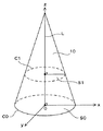
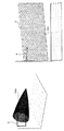
図1は、実施の形態にかかるレドーム10の形状を示す説明図である。本実施の形態では、周波数選択部材として、周波数選択遮蔽性を有するレドームを例にして説明する。図1に示すレドーム10は略円錐形であり、中心軸Lの回転方向に対称な曲面形状を有する。なお、レドーム10は、実際には図14のような流線形をしているが、図1では説明の便宜上、円錐形にモデル化している。レドーム10の底面S0は円形であるが、この中心を原点Oとし、中心軸Lが延びる方向にz軸、底面S0がxy平面上に乗るようにx軸およびy軸をとる。これにより、中心軸Lに対して垂直な任意の面(たとえば面S1)はxy平面上に位置することになる。
(Embodiment)
FIG. 1 is an explanatory diagram illustrating the shape of a
レドーム10には、周波数選択遮蔽性を付与するために、図1に示すような曲面形状のレドーム基材の表面に複数の周波数選択素子が配置される。なお、図示の便宜上、図1には周波数選択素子を示していない。本実施の形態では、周波数選択素子として、線状素子をミアンダ状に配置することにより特定周波数への共振性能を実現したミアンダ化素子を用いる。そして、曲面形状上において規則的配列をおこなうために、ミアンダ化素子のサイズ(配列周期)を変更することにより同一の共振性能を有する大きさの異なる素子を形成し、中心軸Lに対して垂直な任意の面の周上に位置する周波数選択素子の数を等しくしている。
In order to impart frequency selective shielding to the
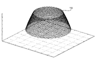
図2および図3は、レドーム10への周波数選択素子の配列例を示す説明図である。図2はレドーム10の全周にわたる配列モデル例を透視図として示し、図3はレドーム10の表面を一方から見た側面図である。図2および図3では、単一の形状のミアンダ化素子を、交互に90°回転させて配列している。また、図2および図3では、円錐の先端部分の図示は省略している。素子の配列周期は上部(円錐形の先端に近い領域)になるほど短くなっており、その分蛇行幅が大きくなることによって、要求される共振特性を満たすだけの素子線長を確保するとともに、下部(円錐形の底面に近い領域)と同じ数の周波数選択素子が配列されている。なお、レドーム10の先端部はごく狭小な面積となるため、本実施の形態による方法とは異なる方法で周波数選択素子を配置する。
2 and 3 are explanatory diagrams showing an example of the arrangement of frequency selection elements on the
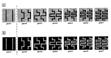
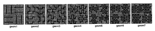
図4は、ミアンダ化素子の形状の一例を示す説明図である。図4において、点線左側のgeom1はミアンダ化前の素子形状、点線右側のgeom2〜geom7はミアンダ化後の素子形状を示している。図4Aおよび図4Bはいずれもダイポール形状の素子(ダイポール素子)であり、geom1に示すミアンダ化前には直線状である形状が、geom2〜geom7に示すミアンダ化後には幅方向に蛇行した形状となっている。この蛇行の幅や蛇行数を変更することにより、任意サイズ(配列周期)のミアンダ化素子を作ることが可能である。なお、図4では、各素子を16×16のセルモデルで示している。配列周期は縦横同サイズとし(tx=ty)、ミアンダ化前の素子として14×1セルのダイポールを2つ配置し、最大7セル幅を使ってミアンダ化をおこなった。 FIG. 4 is an explanatory diagram showing an example of the shape of the meandering element. In FIG. 4, gem1 on the left side of the dotted line indicates the element shape before the meandering, and gem2 to gem7 on the right side of the dotted line indicate the element shape after the meandering. 4A and 4B are both dipole-shaped elements (dipole elements), and the shape that is linear before meandering as shown in geom1 is meandered in the width direction after meandering as shown in gem2 to geom7. It has become. By changing the width of the meander and the number of meanders, a meandering element having an arbitrary size (arrangement period) can be produced. In FIG. 4, each element is shown as a 16 × 16 cell model. The arrangement period was the same size in the vertical and horizontal directions (tx = ty), two 14 × 1 cell dipoles were arranged as elements before the meandering, and the meandering was performed using a maximum width of 7 cells.
図4Aにおいて、素子の形状(ダイポールライン)は金属等の導体素材で形成されている。一方、図4Bは、図4Aと同様のダイポール形状であるが、外周部分が導体素材で形成されており、これに開口する(導体素材を除去する)ことで素子形状を形成する。以下、図4Aのような方法で形状を形成した素子を「パッチ型」、図4Bのような方法で形状を形成した素子を「開口型」という。なお、ダイポールラインを形成する素材は金属以外の導電性インクでも良く、また、用途によっては導体に限らず、半導体特性材料を適用しても良い。 In FIG. 4A, the shape of the element (dipole line) is made of a conductive material such as metal. On the other hand, FIG. 4B has the same dipole shape as FIG. 4A, but the outer peripheral portion is formed of a conductor material, and an element shape is formed by opening the conductor material (removing the conductor material). Hereinafter, an element having a shape formed by the method shown in FIG. 4A is referred to as a “patch type”, and an element formed by the method shown in FIG. 4B is referred to as an “opening type”. The material for forming the dipole line may be a conductive ink other than metal, and depending on the application, not only a conductor but also a semiconductor characteristic material may be applied.
以下の説明では、主に図4Aに示すパッチ型のダイポール素子(以下、単に「ダイポール素子」と言った場合にはパッチ型のダイポール素子を指す)を例にして説明するが、ミアンダ化素子をいかなる形状にするかは、周波数選択素子に要求される特性に合わせて選択すればよい。たとえば、レドーム10に対してバンドパス性能が要求される場合には、周波数選択素子は開口型ミアンダ化素子を用い、バンドストップ性能が要求される場合にはパッチ型ミアンダ化素子を用いればよい。
In the following description, a patch-type dipole element shown in FIG. 4A (hereinafter simply referred to as a “patch-type dipole element”) will be described as an example. What shape should be selected may be selected in accordance with the characteristics required for the frequency selection element. For example, when the band pass performance is required for the
図4Aのgeom1に示すミアンダ化前のダイポール素子は、TE波(ダイポールと平行方向に電界がある)に励起され、ダイポール長が等価的に半波長となる周波数で全反射をおこす一方で、TE波と直交するTM波に関しては全ての周波数で全透過特性を示す。図4Aのgeom2〜geom7に示すミアンダ化後のダイポール素子では、TM波の電界と平行な成分が生じるため、TM波に関しても反射特性を得ることができる。 The dipole element before meandering shown as geom1 in FIG. 4A is excited by a TE wave (there is an electric field in a direction parallel to the dipole), and causes total reflection at a frequency at which the dipole length is equivalent to a half wavelength. For TM waves orthogonal to the waves, all transmission characteristics are exhibited at all frequencies. In the dipole element after the meandering shown in geom2 to geom7 in FIG. 4A, a component parallel to the electric field of the TM wave is generated, so that reflection characteristics can also be obtained for the TM wave.
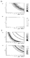
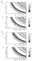
図5は、ミアンダ化前後のパッチ型ダイポール素子における電波透過率の周波数特性を示す説明図である。周波数特性の計算にあたって、周波数範囲は1〜20GHz(0.1GHzステップ)、配列周期は3〜13mm(0.1mmステップ)、入射角0°とした。図5Aはミアンダ化前のダイポール素子(図4Aのgeom1)における周波数特性であり、縦軸は配列周期(素子のサイズ)、横軸は反射波の周波数を示す。図5Aの(a)はTE波、(b)はTM波に対する特性を示す。(b)に示すように、ミアンダ化前のダイポール素子ではTM波に関しては全ての周波数で全透過特性を示す。 FIG. 5 is an explanatory diagram showing the frequency characteristics of the radio wave transmittance in the patch-type dipole element before and after the meandering. In calculating the frequency characteristics, the frequency range was 1 to 20 GHz (0.1 GHz step), the arrangement period was 3 to 13 mm (0.1 mm step), and the incident angle was 0 °. FIG. 5A shows the frequency characteristics of the dipole element (geom1 in FIG. 4A) before the meandering. The vertical axis indicates the arrangement period (element size), and the horizontal axis indicates the frequency of the reflected wave. FIG. 5A shows a characteristic with respect to a TE wave, and FIG. 5B shows a characteristic with respect to a TM wave. As shown in (b), the dipole element before the meandering shows all transmission characteristics at all frequencies with respect to the TM wave.
一方、図5Bはミアンダ化後のダイポール素子(図4Aのgeom7)における周波数特性であり、図5A同様に(a)はTE波、(b)はTM波に対する特性を示す。ミアンダ化後のダイポール素子では、図5B(b)に示すTM波に関しても一部の周波数において反射特性を得られることがわかる。 On the other hand, FIG. 5B shows the frequency characteristics of the dipole element (geom 7 in FIG. 4A) after the meandering, and (a) shows the characteristics with respect to the TE wave and (b) shows the characteristics with respect to the TM wave as in FIG. 5A. In the dipole element after the meandering, it can be seen that reflection characteristics can be obtained at some frequencies even with respect to the TM wave shown in FIG. 5B (b).
任意の形状のミアンダ化素子において特定の周波数に対する共振特性を得たい場合、図5に示す各グラフを参照して、当該形状の素子において所望の周波数に対する反射強度が最大になる配列周期を選択すればよい。 When it is desired to obtain resonance characteristics for a specific frequency in a meandering element having an arbitrary shape, an array period in which the reflection intensity for a desired frequency is maximized is selected with reference to each graph shown in FIG. That's fine.
なお、図4Bに示す開口型ダイポール素子の場合、geom1に示すミアンダ化前の素子ではTM波(ダイポールと直交方向に電界がある)に励起され、ダイポール長が等価的に半波長となる周波数で全反射をおこす一方で、TM波と直交するTE波に関しては透過成分が生じない。一方、図4Bのgeom2〜geom7に示すミアンダ化後の開口型ダイポール素子では、TE波の電界と平行な成分が生じるため、TM波に関しても透過特性を得ることができる。 In the case of the aperture type dipole element shown in FIG. 4B, the element before the meandering shown in geom1 is excited by the TM wave (the electric field is perpendicular to the dipole), and the dipole length is equivalent to a half wavelength. While total reflection occurs, no transmission component is generated for the TE wave orthogonal to the TM wave. On the other hand, in the apertured dipole element after meandering shown in geom2 to geom7 in FIG. 4B, a component parallel to the electric field of the TE wave is generated, so that transmission characteristics can also be obtained for the TM wave.
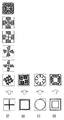
図6は、ミアンダ化素子の他の形状の例を示す説明図である。図6Aはクロスダイポール形状、図6Bは正方形ループ形状、図6Cは円形ループ形状、図6Dは二重正方形ループ形状の素子であり、矢印左側はミアンダ化前の形状、矢印右側はミアンダ化後の形状を示す。ミアンダ化素子は、ダイポール素子に限らず、様々な形状の素子を用いて生成することができる。 FIG. 6 is an explanatory diagram showing another example of the shape of the meandering element. 6A is a cross dipole shape, FIG. 6B is a square loop shape, FIG. 6C is a circular loop shape, and FIG. 6D is a double square loop shape element, the left side of the arrow is the shape before the meandering, the right side of the arrow is the meandered shape Show shape. The meandering element is not limited to a dipole element, and can be generated using elements having various shapes.
ここで、図5にも示したように、ダイポール素子をベースにした周波数選択素子では、TM波に対する特性とTE波に対する特性とが大きく異なる。そこで、ダイポール素子をベースとしたミアンダ化素子を90°回転させた素子を2個ずつ組み合わせて偏波特性が一様となるような両偏波対応型素子を形成して、レドーム10に適用することもできる。すなわち、周波数選択素子を、大きさおよび形状が同一の複数のミアンダ化素子を水平方向および垂直方向に交互に向きを変えて同一数並べた素子群によって形成することも可能である。
Here, as shown also in FIG. 5, in the frequency selection element based on the dipole element, the characteristic for the TM wave and the characteristic for the TE wave are greatly different. Therefore, by combining two elements obtained by rotating 90 ° of the meandering elements based on the dipole elements, a dual-polarization-compatible element with uniform polarization characteristics is formed and applied to the
図7および図8は、両偏波対応型素子の形状の一例を示す説明図である。図7および図8では、図4Aに示した16×16セルの周波数選択素子を4つ集合させた32×32セルで1つの周波数選択素子を構成している。図4Aと同様に、配列周期は縦横同サイズとし(tx=ty)、ミアンダ化前の素子として14×1セルのダイポールを1ユニット(16×16セル)に2つ配置し、最大7セル幅を使ってミアンダ化をおこなった。これを90°回転させて図7および図8に示す素子を得る。図7のgeom1〜geom7では、右側に位置する素子形状ほど素子の蛇行数が多くなっている。 7 and 8 are explanatory diagrams showing an example of the shape of the dual-polarization compatible element. 7 and 8, one frequency selection element is configured by 32 × 32 cells in which four 16 × 16 cell frequency selection elements shown in FIG. 4A are assembled. Similar to FIG. 4A, the arrangement period is the same size in the vertical and horizontal directions (tx = ty), and two 14 × 1 cell dipoles are arranged in one unit (16 × 16 cells) as the element before the meandering, and the maximum cell width is 7 cells. The meandering was done using. This is rotated 90 ° to obtain the elements shown in FIGS. In geom1 to geom7 in FIG. 7, the number of meandering elements increases as the element shape is located on the right side.
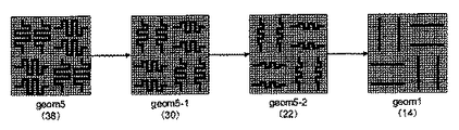
また、図8のgeom5、geom5−1、geom5−2、geom1は、図7のgeom5に示した2周期分蛇行しているミアンダ化素子について、蛇行幅を変更した例であり、右側に位置する素子形状ほど素子の蛇行幅が小さくなり、最も右側に位置するgeom1はミアンダ化前のダイポール素子形状となっている。すなわち、図8に示す素子群は、同一のミアンダ形状において蛇行幅および素子線長を異ならせた相似形ミアンダ化素子群である。
Further, gemom5, gemom5-1, gemom5-2, and gemom1 in FIG. 8 are examples in which the meandering width of the meandering element meandering for two cycles shown in gem5 in FIG. 7 is changed and is located on the right side. The meandering width of the element becomes smaller as the element shape becomes, and the
図9は、両偏波対応型素子における電波透過率の周波数特性を示す説明図である。周波数特性の計算にあたって、周波数範囲は1〜20GHz(0.1GHzステップ)、配列周期は6〜26mm(0.1mmステップ)、入射角0°とした。図9Aは図8のgeom5−1、図9Bはgeom5−2に示した両偏波対応型素子の周波数特性を示している。縦軸および横軸は、それぞれ配列周期(素子のサイズ)および反射波の周波数を示している。また、各図において(a)はTE波、(b)はTM波に対する特性をそれぞれ示している。図9AおよびBに示すように、両偏波対応型素子では、TE波およびTM波に対する特性が、ほぼ一致している。 FIG. 9 is an explanatory diagram showing the frequency characteristics of radio wave transmittance in the dual-polarization type element. In calculating the frequency characteristics, the frequency range was 1 to 20 GHz (0.1 GHz step), the array period was 6 to 26 mm (0.1 mm step), and the incident angle was 0 °. FIG. 9A shows the frequency characteristics of the both-polarization-compatible element shown in FIG. 8 gem 5-1 and FIG. 9B shows the gem 5-2. The vertical axis and the horizontal axis indicate the arrangement period (element size) and the frequency of the reflected wave, respectively. In each figure, (a) shows the characteristics for the TE wave, and (b) shows the characteristics for the TM wave. As shown in FIGS. 9A and 9B, the characteristics with respect to the TE wave and the TM wave are substantially the same in both polarization-compatible elements.
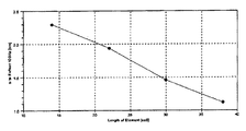
図10は、図8に示した相似形ミアンダ化素子群について、所定の周波数をターゲットとした場合の各周波数選択素子における配列周期と素子線長との関係を示す表である。上述したように、特定の周波数に対する反射特性を得たい場合、当該形状の素子において所望の周波数に対する反射強度が最大になる配列周期を選択すればよい。図10は10GHzをターゲットとした場合の配列周期tx(=ty)と素子線長(セル数および実際の線長)とを示す。 FIG. 10 is a table showing the relationship between the arrangement period and the element line length in each frequency selection element when a predetermined frequency is targeted for the similar meandering element group shown in FIG. As described above, when it is desired to obtain reflection characteristics for a specific frequency, an array period that maximizes the reflection intensity for a desired frequency in the element having the shape may be selected. FIG. 10 shows the arrangement period tx (= ty) and the element line length (number of cells and actual line length) when targeting 10 GHz.
図11は、図10に示した配列周期と素子線長(セル数)とをプロットしたグラフである。図11において、縦軸は配列周期、横軸は素子線長(セル数)である。図11に示すように、相似形ミアンダ化素子群では、配列周期とセル数で示した素子線長(セル数)とはほぼ線形に比例している。すなわち、この線形関係から任意の配列周期に応じた素子線長(セル数)を決定することが可能である。 FIG. 11 is a graph in which the arrangement period and the element line length (number of cells) shown in FIG. 10 are plotted. In FIG. 11, the vertical axis represents the arrangement period, and the horizontal axis represents the element line length (number of cells). As shown in FIG. 11, in the similar meandering element group, the arrangement period and the element line length (number of cells) indicated by the number of cells are substantially linearly proportional. That is, it is possible to determine the element line length (number of cells) corresponding to an arbitrary arrangement period from this linear relationship.
具体的には、配列周期をx、素子線長(セル数)をyとして線形回帰し、下記式(1)に示す回帰式を設定する。下記式(1)において、txは配列周期、Lcellは素子線長(セル数)、AおよびBは定数である。上記式(1)に所望の配列周期を代入すれば、対応する素子線長をセル数単位で求めることができる。
Lcell=Atx+B・・・(1)
Specifically, linear regression is performed by setting the array period as x and the element line length (number of cells) as y, and the regression equation shown in the following formula (1) is set. In the following formula (1), tx is an array period, Lcell is an element line length (number of cells), and A and B are constants. If a desired arrangement period is substituted into the above equation (1), the corresponding element line length can be determined in units of cells.
Lcell = Atx + B (1)
つぎに、上記式(1)で算出した全体の素子線長(セル数)からミアンダラインの蛇行幅を求める。ミアンダラインの蛇行幅(すなわち、元のダイポールと直交する方向に描かれるセル数)は、全体の素子線長(セル数)から元のダイポール長(セル数)を差し引き、元のダイポールと直交する方向に描かれる線の本数(蛇行数)で除せばよい。すなわち、ミアンダラインの蛇行幅をLcross、全体の素子線長(セル数)をLcell、元のダイポール長(セル数)をLdip、元のダイポールと直交する方向に描かれる線の本数(蛇行数)をNwとすると、下記式(2)で示すことができる。なお、Nwは、蛇行幅分の長さを有する線を1本としてカウントする。たとえば、ミアンダラインの始端および終端近傍の蛇行ラインは、蛇行幅の半分の長さであり、この場合は0.5とカウントする。
Lcross=(Lcell−Ldip)/Nw・・・(2)
Next, the meander line meandering width is obtained from the total element line length (number of cells) calculated by the above equation (1). The meander line meandering width (ie, the number of cells drawn in a direction perpendicular to the original dipole) is orthogonal to the original dipole by subtracting the original dipole length (cell number) from the total element line length (cell number). Divide by the number of lines drawn in the direction (meander number). That is, the meander line meandering width is Lcross, the entire element line length (number of cells) is Lcell, the original dipole length (number of cells) is Ldip, and the number of lines drawn in the direction perpendicular to the original dipole (number of meandering) Can be expressed by the following formula (2). Nw is counted as one line having a length corresponding to the meandering width. For example, the meander line near the beginning and end of the meander line is half the meander width, and in this case it is counted as 0.5.
Lcross = (Lcell-Ldip) / Nw (2)
セル数で示した線長Lcellは、下記式(3)によって実際の線長(以下「実長」という)Lactに変換することができる。下記式(3)において、Ncellは素子モデルの1辺におけるセル数(図5の例では32)である。
Lact=tx×Lcell/Ncell・・・(3)
The line length Lcell indicated by the number of cells can be converted into an actual line length (hereinafter referred to as “actual length”) Lact by the following equation (3). In the following formula (3), Ncell is the number of cells on one side of the element model (32 in the example of FIG. 5).
Lact = tx × Lcell / Ncell (3)
すなわち、上記式(2)で示した蛇行幅Lcrossを実長で示す場合は、下記式(2’)のように求めることができる。
Lcross={(Lcell−Ldip)/Nw}×(tx/Ncell)・・・(2’)
That is, when the meandering width Lcross shown in the above equation (2) is indicated by the actual length, it can be obtained as in the following equation (2 ′).
Lcross = {(Lcell-Ldip) / Nw} × (tx / Ncell) (2 ′)
上記式を用いて、図8に示した素子形状について、任意の配列周期における蛇行幅の算出手順の具体例を示す。まず、図11に示した線形関係を回帰式とすると、下記式(1’)で示すことができる。
Lcell=−19.815tx+59.784・・・(1’)
A specific example of the procedure for calculating the meandering width in an arbitrary arrangement period for the element shape shown in FIG. 8 will be described using the above formula. First, when the linear relationship shown in FIG. 11 is a regression equation, it can be expressed by the following equation (1 ′).
Lcell = −19.815tx + 59.784 (1 ′)
上記式(1)に所望の配列周期を代入すれば、対応する素子線長をセル数単位で求めることができる。たとえば、配列周期1.7cmにしたいときには、上記式(1’)を用いてLcell=26.099と求めることができる。 If a desired arrangement period is substituted into the above equation (1), the corresponding element line length can be determined in units of cells. For example, when it is desired to set the arrangement period to 1.7 cm, Lcell = 26.099 can be obtained using the above formula (1 ′).
図8に示した周波数選択素子は、Ldip=14、Nw=4なので、上記式(1’)を用いて求めたLcell=26.099および上記式(2)から、Lcross=3.02(セル数)と求めることができる。さらに、tx=1.7cm、Ncell=32から、上記式(2’)を用いて、蛇行幅の実長を1.6mmと求めることができる。 Since the frequency selection element shown in FIG. 8 is Ldip = 14 and Nw = 4, Lcell = 26.099 obtained using the above equation (1 ′) and the above equation (2), Lcross = 3.02 (cell Number). Furthermore, from tx = 1.7 cm and Ncell = 32, the actual length of the meandering width can be obtained as 1.6 mm using the above formula (2 ′).
以上のような手順により、任意の形状のミアンダ化素子について、任意の配列周期における蛇行寸法を設定することが可能となる。図1に示したレドーム10では、曲面形状上において規則的配列をおこなうために、ミアンダ化素子の配列周期を変更することにより同一の共振性能を有する大きさの異なる素子を形成し、中心軸Lに対して垂直な任意の面の周上に位置する周波数選択素子の数を等しくしている。具体的には、たとえばレドーム10の底面S0の周C0上に位置する周波数選択素子の数と、中心軸Lに対して垂直な面S1の周C1に位置する周波数選択素子の数を等しくする。これにより、周波数選択素子をシミュレーション等によって性能を評価しうる規則的な配列に置くことができる。
With the above procedure, it is possible to set a meandering dimension in an arbitrary arrangement period for a meandering element having an arbitrary shape. In the
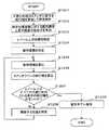
図12は、ミアンダ化素子である周波数選択素子の配列モデルの算出方法の手順を示すフローチャートである。図12のフローチャートにおいて、まず、任意の形状のミアンダ化素子について、蛇行幅を一定間隔で変更して特性解析をおこなう(ステップS1201:特性算出工程)。ステップS1201では、ミアンダ化素子の蛇行幅を一定間隔で変更した(図8のgeom5,geom5−1,geom5−2,geom1のような)モデルを生成し、図9に示すような電波透過率の周波数特性をそれぞれ算出する。 FIG. 12 is a flowchart illustrating a procedure of a method for calculating an array model of frequency selection elements that are meandering elements. In the flowchart of FIG. 12, first, characteristic analysis is performed on the meandering element having an arbitrary shape by changing the meandering width at regular intervals (step S1201: characteristic calculation step). In step S1201, a model in which the meandering width of the meandering element is changed at regular intervals (such as geom5, geom5-1, geom5-2, and geom1 in FIG. 8) is generated, and the radio wave transmittance as shown in FIG. Each frequency characteristic is calculated.
つぎに、ステップS1201で算出した周波数特性に基づいて、特定の周波数に対する配列周期と素子線長との回帰式を算出する(ステップS1202:回帰式算出工程)。ステップS1202では、まず、周波数選択素子に要求される性能に基づいてターゲットとする周波数を選択する。そして、各モデルにおいて当該選択周波数で共振性能が得られる配列周期を特定し、当該モデルにおける素子線長(セル数)と配列周期との関係を示す回帰式、すなわち上記式(1)を線形回帰によって算出する。 Next, based on the frequency characteristic calculated in step S1201, a regression equation between the array period and the element line length for a specific frequency is calculated (step S1202: regression equation calculation step). In step S1202, first, a target frequency is selected based on the performance required for the frequency selection element. Then, in each model, an array period in which resonance performance is obtained at the selected frequency is specified, and a regression equation showing the relationship between the element line length (number of cells) and the array period in the model, ie, the above equation (1) is linearly regressed. Calculated by
つづいて、周波数選択素子が配列されるレドーム10上の位置を特定する(ステップS1203)。最初に特定するレドーム10上の位置は、たとえば円錐の底面S0近傍(底面の周C0上)とする。レドーム10のサイズは既知であるため、周波数選択素子が配列されるレドーム10上の位置が特定されれば、その位置を含み、レドーム10の中心軸Lに対して垂直な面の周の長さを特定することができる。
Subsequently, the position on the
つぎに、レドーム10の同一周上に配置する周波数選択素子の配列個数を決定する(ステップS1204:素子数決定工程)。なお、周波数選択素子の配列個数は、全ての周上において同一とする。そして、ステップS1203で特定された位置の周の長さを、周波数選択素子の配列個数で除すことによって周波数選択素子の配列周期txを算出する(ステップS1205:配列周期決定工程)。
Next, the number of frequency selection elements arranged on the same circumference of the
つぎに、ステップS1202で算出した回帰式およびステップS1205で算出した配列周期txとを用いて、上述した手順(上記式(2)および(3)参照)によりミアンダラインの蛇行幅を算出する(ステップS1206:蛇行幅算出工程)。これにより、ステップS1203で特定された位置における周波数選択素子の配列が決定する。 Next, using the regression equation calculated in step S1202 and the array period tx calculated in step S1205, the meander line meander width is calculated according to the above-described procedure (see the above equations (2) and (3)) (step S1206: Meander width calculation step). As a result, the arrangement of the frequency selection elements at the position specified in step S1203 is determined.
レドーム10上の全ての位置に配列される周波数選択素子の蛇行幅を決定するまでは(ステップS1207:No)、ステップS1203で特定された位置と隣接する位置(より詳細には、ステップS1203で特定された位置に配列される周波数選択素子の端部に隣接する位置)を特定し(ステップS1208)、この位置について、ステップS1205以降に示す処理をくり返す。
Until the meandering width of the frequency selection elements arranged at all positions on the
そして、レドーム10上の全ての位置に配列される周波数選択素子の蛇行幅を決定すると(ステップS1207:Yes)、レドーム10上の周波数選択素子の配列モデルが完成したものとして(ステップS1209)、本フローチャートによる処理を終了する。
When the meandering width of the frequency selection elements arranged at all positions on the
以上説明したように、実施の形態にかかるレドーム10は、中心軸の回転方向に対称な曲面形状を有する基材に周波数選択素子を配列する際に、周波数選択素子を、線状素子をミアンダ形状に配置することにより特定周波数への共振性能を実現したミアンダ化素子とした。そして、ミアンダ形状のサイズを変更することにより同一の共振性能を有する大きさの異なる素子を形成し、中心軸に対して垂直な任意の面の周上に位置する周波数選択素子の数を等しくした。これにより、レドーム基材が曲面形状を有する場合でも周波数選択素子の規則的配列を保つことができ、シミュレーション等による性能評価の精度を向上させることができる。
As described above, in the
また、レドーム10に配列される周波数選択素子は、大きさおよび形状が同一の複数のミアンダ化素子を水平方向および垂直方向に交互に向きを変えて同一数並べた素子群(両偏波対応型素子)によって形成される。これにより、TE波およびTM波に対する特性をほぼ一致させることができる。
In addition, the frequency selection elements arranged in the
また、レドーム10に対してバンドパス性能が要求される場合には、周波数選択素子は開口型ミアンダ化素子を用い、バンドストップ性能が要求される場合にはパッチ型ミアンダ化素子を用いることによって、要求される性能を満たすレドームを得ることができる。
Further, when the band pass performance is required for the
また、実施の形態にかかる周波数選択素子の配列決定方法によれば、中心軸の回転方向に対称な曲面形状を有するレドーム10の中心軸Lに対して垂直な面の周上における周波数選択素子の素子数を決定し、決定された素子数に基づいて、各周上における周波数選択素子の配列周期を決定し、決定された配列周期において周波数選択素子に要求される共振性能を実現するミアンダ形状を決定する。これにより、レドーム基材が曲面形状を有する場合でも周波数選択素子の規則的配列を保つことができ、シミュレーション等による性能評価の精度を向上させることができる。
Further, according to the method for determining the arrangement of the frequency selection elements according to the embodiment, the frequency selection elements on the circumference of the plane perpendicular to the central axis L of the
また、実施の形態にかかる周波数選択素子の配列決定方法によれば、同一のミアンダ形状において蛇行幅および素子線長を異ならせた相似形ミアンダ化素子群を形成し、相似形ミアンダ化素子群内のそれぞれのミアンダ化素子について、配列周期に基づく電波透過率の周波数特性を算出し、算出された周波数特性に基づいて、特定周波数における素子線長と配列周期との線形回帰をおこない、素子線長と配列周期との回帰式を算出し、当該回帰式と周の長さに合わせて決定された配列周期とに基づいて、配列周期に対応する素子線長および蛇行幅を算出する。これにより、任意の周上に配列可能かつ要求される共振性能を有するミアンダ化素子を得ることができる。 Further, according to the method of determining the arrangement of the frequency selection elements according to the embodiment, the similar meandering element group in which the meandering width and the element line length are different in the same meander shape is formed, and in the similar meandering element group For each of the meandering elements, the frequency characteristic of the radio wave transmittance based on the array period is calculated, and based on the calculated frequency characteristic, linear regression between the element line length and the array period at a specific frequency is performed, and the element line length And the element line length and the meandering width corresponding to the array period are calculated based on the regression expression and the array period determined in accordance with the circumference. Thereby, a meandering element that can be arranged on an arbitrary circumference and has the required resonance performance can be obtained.
なお、本実施の形態では、周波数選択部材としてレドームを挙げて説明したが、本発明は従来公知の様々な周波数選択部材(すなわち透過周波数帯選択性を有する部材)に適用可能である。具体的には、周波数選択部材は、たとえばレドームをはじめとする電磁窓や電波吸収体に適用することができる。周波数選択部材を電磁窓として用いる例については、上述した実施の形態の通りである。また、周波数選択部材を電波吸収体に適用する例としては、たとえば特許第4144940号公報等に開示されている航空機の主翼前縁部への適用などが挙げられる。 In the present embodiment, a radome has been described as the frequency selection member. However, the present invention can be applied to various conventionally known frequency selection members (that is, members having transmission frequency band selectivity). Specifically, the frequency selection member can be applied to an electromagnetic window such as a radome or a radio wave absorber. An example in which the frequency selection member is used as an electromagnetic window is as described in the above embodiment. Moreover, as an example which applies a frequency selection member to a radio wave absorber, the application to the main wing leading edge part of the aircraft currently disclosed by patent 4144940 etc. is mentioned, for example.
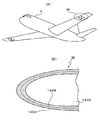
図13は、電波吸収体の航空機への適用例を示す説明図である。図13Aに示す航空機Fの主翼前縁部Wには電波吸収体が装備されている。図13Bは主翼前縁部Wの断面図であり、主翼の基材である導体部1402の表面に電波吸収層1404が設けられている。電波吸収層1404は、内部に周波数選択素子1406が本発明の方法で配置されることにより、電波吸収性能が得られる。本発明を電波吸収体に適用することによって、電波吸収性能を発揮する帯域の広域化や、構造の薄肉化による軽量化、方位特性の向上などを図ることができる。
FIG. 13 is an explanatory diagram showing an application example of the radio wave absorber to an aircraft. The main wing leading edge W of the aircraft F shown in FIG. 13A is equipped with a radio wave absorber. FIG. 13B is a cross-sectional view of the main wing leading edge W, and a radio
また、本実施の形態では、レドーム10の曲面形状を、中心軸の回転方向に対称な形状として、中心軸に対して垂直な任意の面の周上に位置する周波数選択素子の数を等しくしたが、本発明の適用はこのような回転対称な曲面形状に限られない。本発明を任意の曲面形状に適用する場合、この曲面形状を通る(任意の)軸に対して垂直な任意の面の周上に位置する周波数選択素子の数を等しくすれば、本実施の形態と同様の効果が得られる。
Further, in the present embodiment, the curved surface shape of the
10……レドーム、C0,C1……周、L……中心軸、O……原点、S0……底面、S1……面。 10: radome, C0, C1: circumference, L: central axis, O: origin, S0: bottom surface, S1: surface.
Claims (7)
前記曲面形状の周波数選択部材用基材と、
前記周波数選択部材用基材の表面に配置された複数の周波数選択素子と、を備え、
前記周波数選択素子は、線状素子をミアンダ形状に配置することにより特定周波数への共振性能を実現したミアンダ化素子であり、前記ミアンダ形状のサイズを変更することにより同一の前記共振性能を有する大きさの異なる素子を形成し、前記曲面形状を通る軸に対して垂直な任意の面の周上に位置する前記周波数選択素子の数を等しくしたことを特徴とする周波数選択部材。 A frequency selection member having a curved shape,
A base material for a frequency selective member having a curved surface;
A plurality of frequency selection elements arranged on the surface of the base material for the frequency selection member,
The frequency selection element is a meandering element that realizes resonance performance to a specific frequency by arranging linear elements in a meander shape, and has the same resonance performance by changing the size of the meander shape. A frequency selection member characterized in that the number of the frequency selection elements formed on the circumference of an arbitrary surface that is formed with different elements and is perpendicular to an axis passing through the curved surface shape is equal.
前記中心軸に対して垂直な任意の面の周上に位置する前記周波数選択素子の数を等しくしたことを特徴とする請求項1〜4のいずれか一つに記載の周波数選択部材。 The curved surface shape is a symmetrical shape with respect to the rotation direction of the central axis,
The frequency selection member according to any one of claims 1 to 4, wherein the number of the frequency selection elements located on the circumference of an arbitrary surface perpendicular to the central axis is made equal.
前記周波数選択素子は、線状素子をミアンダ形状に配置することにより特定周波数への共振性能を実現したミアンダ化素子であり、
前記曲面を通る軸に対して垂直な面の周上における前記周波数選択素子の素子数を決定する素子数決定工程と、
前記素子数決定工程で決定された前記素子数に基づいて、各周上における前記周波数選択素子の配列周期を決定する配列周期決定工程と、
前記配列周期決定工程で決定された前記配列周期において前記周波数選択素子に要求される前記共振性能を実現する前記ミアンダ形状を決定する形状決定工程と、
を含んだことを特徴とする周波数選択素子の配列決定方法。 A method for determining the arrangement of frequency selective elements on a curved surface,
The frequency selection element is a meandering element that realizes resonance performance to a specific frequency by arranging linear elements in a meander shape,
An element number determination step for determining the number of the frequency selection elements on a circumference of a surface perpendicular to an axis passing through the curved surface;
An array period determining step for determining an array period of the frequency selection elements on each circumference based on the number of elements determined in the element number determining step;
A shape determining step for determining the meander shape that realizes the resonance performance required for the frequency selection element in the array cycle determined in the array cycle determining step;
A method for determining the arrangement of frequency selective elements.
同一の前記ミアンダ形状において蛇行幅および素子線長を異ならせた相似形ミアンダ化素子群を形成し、前記相似形ミアンダ化素子群内のそれぞれの前記ミアンダ化素子について、配列周期に基づく電波透過率の周波数特性を算出する特性算出工程と、
前記特性算出工程で算出された前記周波数特性に基づいて、特定周波数における前記素子線長と前記配列周期との線形回帰をおこない、前記素子線長と前記配列周期との回帰式を算出する回帰式算出工程と、
前記回帰式算出工程で算出された前記回帰式と前記配列周期決定工程で決定された前記配列周期とに基づいて、前記配列周期に対応する前記素子線長および前記蛇行幅を算出する蛇行幅算出工程と、
を含むことを特徴とする請求項6に記載の周波数選択素子の配列決定方法。 The shape determination step includes
A similar meandering element group having different meandering widths and element line lengths in the same meander shape is formed. A characteristic calculation step for calculating the frequency characteristic of
Based on the frequency characteristic calculated in the characteristic calculation step, a linear regression between the element line length and the array period at a specific frequency is performed, and a regression equation for calculating a regression equation between the element line length and the array period A calculation process;
Based on the regression equation calculated in the regression equation calculation step and the array cycle determined in the array cycle determination step, the meander width calculation for calculating the element line length and the meander width corresponding to the array cycle Process,
The method for determining the arrangement of frequency selective elements according to claim 6, comprising:
Priority Applications (1)
| Application Number | Priority Date | Filing Date | Title |
|---|---|---|---|
| JP2012277612A JP6142522B2 (en) | 2012-12-20 | 2012-12-20 | Frequency selection member and method for determining frequency selection element arrangement on curved surface |
Applications Claiming Priority (1)
| Application Number | Priority Date | Filing Date | Title |
|---|---|---|---|
| JP2012277612A JP6142522B2 (en) | 2012-12-20 | 2012-12-20 | Frequency selection member and method for determining frequency selection element arrangement on curved surface |
Publications (2)
| Publication Number | Publication Date |
|---|---|
| JP2014123793A true JP2014123793A (en) | 2014-07-03 |
| JP6142522B2 JP6142522B2 (en) | 2017-06-07 |
Family
ID=51403976
Family Applications (1)
| Application Number | Title | Priority Date | Filing Date |
|---|---|---|---|
| JP2012277612A Active JP6142522B2 (en) | 2012-12-20 | 2012-12-20 | Frequency selection member and method for determining frequency selection element arrangement on curved surface |
Country Status (1)
| Country | Link |
|---|---|
| JP (1) | JP6142522B2 (en) |
Cited By (11)
| Publication number | Priority date | Publication date | Assignee | Title |
|---|---|---|---|---|
| GB2539279A (en) * | 2015-06-12 | 2016-12-14 | Secr Defence | Frequency selective surface for reducing antenna coupling |
| JP2018113558A (en) * | 2017-01-11 | 2018-07-19 | 日本電信電話株式会社 | Electromagnetic field band filter |
| JP2018191281A (en) * | 2017-05-01 | 2018-11-29 | パロ アルト リサーチ センター インコーポレイテッド | Multi-band radio frequency transparency window in conductive film |
| KR102021381B1 (en) * | 2018-05-31 | 2019-09-16 | 공주대학교 산학협력단 | Radome that adopting fss structure to prevent gps jamming |
| CN110797666A (en) * | 2019-11-05 | 2020-02-14 | 南京邮电大学 | Gravitational Field Controlled Wave Absorber and Frequency Selective Reconfigurable Device |
| CN110889216A (en) * | 2019-11-20 | 2020-03-17 | 上海无线电设备研究所 | Adaptive rapid design method for curved surface frequency selection surface radome |
| CN113314848A (en) * | 2021-04-17 | 2021-08-27 | 西安电子科技大学 | Conformal layout and modeling method of frequency selective surface |
| CN115764314A (en) * | 2022-11-07 | 2023-03-07 | 东南大学 | Low-cost stretchable angle-insensitive flexible frequency selection surface |
| CN117424002A (en) * | 2023-12-19 | 2024-01-19 | 四川九洲电器集团有限责任公司 | Design and use methods of 0-90-degree conformal FSS plate and FSS plate |
| WO2025127780A1 (en) * | 2023-12-12 | 2025-06-19 | 아주대학교산학협력단 | Electromagnetic wave transmission heater for selectively transmitting frequency |
| CN120280700A (en) * | 2025-06-09 | 2025-07-08 | 南京信息工程大学 | Ultrathin single-layer double-passband frequency selective surface structure |
Citations (13)
| Publication number | Priority date | Publication date | Assignee | Title |
|---|---|---|---|---|
| JPH06226477A (en) * | 1992-06-22 | 1994-08-16 | Martin Marietta Corp | Removing method for printing clrcuit board technology |
| JPH06260739A (en) * | 1992-06-26 | 1994-09-16 | Martin Marietta Corp | Direct image formation of three-dimensional circuit and same thing |
| JP2001298322A (en) * | 2000-04-11 | 2001-10-26 | Sumitomo Electric Ind Ltd | Aircraft radome |
| JP2002033592A (en) * | 2000-07-14 | 2002-01-31 | Murata Mfg Co Ltd | Electromagnetic-wave cutoff structure |
| JP2006258449A (en) * | 2005-03-15 | 2006-09-28 | Yokohama Rubber Co Ltd:The | Radome |
| US20070200787A1 (en) * | 2006-02-24 | 2007-08-30 | Williams Victor G | Thermoformed frequency selective surface |
| JP2008536366A (en) * | 2005-03-15 | 2008-09-04 | エレクトロニクス アンド テレコミュニケーションズ リサーチ インスチチュート | Frequency selective reflector for frequency band filtering and design method thereof |
| JP2009043984A (en) * | 2007-08-09 | 2009-02-26 | Tohoku Kako Kk | Composite type radio wave absorber |
| US20090110265A1 (en) * | 2007-10-11 | 2009-04-30 | Raytheon Company | System for Forming Patterns on a Multi-Curved Surface |
| US20100097048A1 (en) * | 2007-01-04 | 2010-04-22 | Werner Douglas H | Passive detection of analytes |
| US20100253564A1 (en) * | 2007-10-26 | 2010-10-07 | James Christopher Gordon Matthews | Reducing radar signatures |
| JP2013527694A (en) * | 2010-04-27 | 2013-06-27 | インスティチュート ポリテクニック デ グレノーブル | Surface for filtering multiple frequency bands |
| JP2014155102A (en) * | 2013-02-12 | 2014-08-25 | Yokohama Rubber Co Ltd:The | Method of determining arrangement of frequency selection elements on curved surface |
-
2012
- 2012-12-20 JP JP2012277612A patent/JP6142522B2/en active Active
Patent Citations (14)
| Publication number | Priority date | Publication date | Assignee | Title |
|---|---|---|---|---|
| US5472828A (en) * | 1992-06-22 | 1995-12-05 | Martin Marietta Corporation | Ablative process for printed circuit board technology |
| JPH06226477A (en) * | 1992-06-22 | 1994-08-16 | Martin Marietta Corp | Removing method for printing clrcuit board technology |
| JPH06260739A (en) * | 1992-06-26 | 1994-09-16 | Martin Marietta Corp | Direct image formation of three-dimensional circuit and same thing |
| JP2001298322A (en) * | 2000-04-11 | 2001-10-26 | Sumitomo Electric Ind Ltd | Aircraft radome |
| JP2002033592A (en) * | 2000-07-14 | 2002-01-31 | Murata Mfg Co Ltd | Electromagnetic-wave cutoff structure |
| JP2008536366A (en) * | 2005-03-15 | 2008-09-04 | エレクトロニクス アンド テレコミュニケーションズ リサーチ インスチチュート | Frequency selective reflector for frequency band filtering and design method thereof |
| JP2006258449A (en) * | 2005-03-15 | 2006-09-28 | Yokohama Rubber Co Ltd:The | Radome |
| US20070200787A1 (en) * | 2006-02-24 | 2007-08-30 | Williams Victor G | Thermoformed frequency selective surface |
| US20100097048A1 (en) * | 2007-01-04 | 2010-04-22 | Werner Douglas H | Passive detection of analytes |
| JP2009043984A (en) * | 2007-08-09 | 2009-02-26 | Tohoku Kako Kk | Composite type radio wave absorber |
| US20090110265A1 (en) * | 2007-10-11 | 2009-04-30 | Raytheon Company | System for Forming Patterns on a Multi-Curved Surface |
| US20100253564A1 (en) * | 2007-10-26 | 2010-10-07 | James Christopher Gordon Matthews | Reducing radar signatures |
| JP2013527694A (en) * | 2010-04-27 | 2013-06-27 | インスティチュート ポリテクニック デ グレノーブル | Surface for filtering multiple frequency bands |
| JP2014155102A (en) * | 2013-02-12 | 2014-08-25 | Yokohama Rubber Co Ltd:The | Method of determining arrangement of frequency selection elements on curved surface |
Cited By (13)
| Publication number | Priority date | Publication date | Assignee | Title |
|---|---|---|---|---|
| GB2539279A (en) * | 2015-06-12 | 2016-12-14 | Secr Defence | Frequency selective surface for reducing antenna coupling |
| JP2018113558A (en) * | 2017-01-11 | 2018-07-19 | 日本電信電話株式会社 | Electromagnetic field band filter |
| JP2018191281A (en) * | 2017-05-01 | 2018-11-29 | パロ アルト リサーチ センター インコーポレイテッド | Multi-band radio frequency transparency window in conductive film |
| KR102021381B1 (en) * | 2018-05-31 | 2019-09-16 | 공주대학교 산학협력단 | Radome that adopting fss structure to prevent gps jamming |
| CN110797666A (en) * | 2019-11-05 | 2020-02-14 | 南京邮电大学 | Gravitational Field Controlled Wave Absorber and Frequency Selective Reconfigurable Device |
| CN110889216B (en) * | 2019-11-20 | 2023-11-14 | 上海无线电设备研究所 | Self-adaptive rapid design method for curved surface frequency selective surface radome |
| CN110889216A (en) * | 2019-11-20 | 2020-03-17 | 上海无线电设备研究所 | Adaptive rapid design method for curved surface frequency selection surface radome |
| CN113314848A (en) * | 2021-04-17 | 2021-08-27 | 西安电子科技大学 | Conformal layout and modeling method of frequency selective surface |
| CN113314848B (en) * | 2021-04-17 | 2022-10-18 | 西安电子科技大学 | Conformal layout and modeling method of frequency selective surface |
| CN115764314A (en) * | 2022-11-07 | 2023-03-07 | 东南大学 | Low-cost stretchable angle-insensitive flexible frequency selection surface |
| WO2025127780A1 (en) * | 2023-12-12 | 2025-06-19 | 아주대학교산학협력단 | Electromagnetic wave transmission heater for selectively transmitting frequency |
| CN117424002A (en) * | 2023-12-19 | 2024-01-19 | 四川九洲电器集团有限责任公司 | Design and use methods of 0-90-degree conformal FSS plate and FSS plate |
| CN120280700A (en) * | 2025-06-09 | 2025-07-08 | 南京信息工程大学 | Ultrathin single-layer double-passband frequency selective surface structure |
Also Published As
| Publication number | Publication date |
|---|---|
| JP6142522B2 (en) | 2017-06-07 |
Similar Documents
| Publication | Publication Date | Title |
|---|---|---|
| JP6142522B2 (en) | Frequency selection member and method for determining frequency selection element arrangement on curved surface | |
| Sabah et al. | Polarization-insensitive FSS-based perfect metamaterial absorbers for GHz and THz frequencies | |
| KR20100134583A (en) | Lens for scanning angle enhancement of phased array antenna | |
| JP5410558B2 (en) | Reflect array and design method | |
| JP5410559B2 (en) | Reflect array and design method | |
| Liu et al. | RCS reduction of a patch array antenna based on microstrip resonators | |
| De Cos et al. | On the advantages of loop-based unit-cell’s metallization regarding the angular stability of artificial magnetic conductors | |
| Babu et al. | Deep learning assisted fractal slotted substrate MIMO antenna with characteristic mode analysis (CMA) for Sub-6 GHz n78 5 G NR applications: design, optimization and experimental validation | |
| Devi et al. | Liquid crystal polymer based flexible and conformal 5G antenna for vehicular communication | |
| CN108539424A (en) | Dual band frequencies select composite material sandwich structure and its manufacturing method | |
| KR101587251B1 (en) | Device for absorbing frequency selective wave independent of the angle of incidence and manufacturing method thereof | |
| TR201412400A1 (en) | Fast and accurate design method for broadband multi-layered radar absorbers. | |
| Ahsan et al. | Metasurface reflector (MSR) loading for high performance small microstrip antenna design | |
| Solunke et al. | An ultra-thin, low-RCS, dual-bandpass novel fractal-FSS for planar/conformal C&X bands applications | |
| JP5398858B2 (en) | Reflect array and design method | |
| Sheng et al. | Design of frequency selective rasorber with wide transmission/absorption bands | |
| CN114142246B (en) | A wide-band and large-angle metamaterial absorber based on gradient impedance and its preparation method | |
| Liu et al. | A metamaterial absorber with centre-spin design and characteristic modes analysis | |
| Habib Ullah et al. | A new metasurface reflective structure for simultaneous enhancement of antenna bandwidth and gain | |
| Palanisamy et al. | Design of Artificial Magnetic Conductor based Stepped V-shaped Printed multiband antenna for Wireless Applications. | |
| JP2014217031A (en) | Reflection plate and antenna apparatus | |
| KR20090116347A (en) | Transmissive Electromagnetic Refractor | |
| JP5938012B2 (en) | Reflector and antenna device | |
| CN102751581B (en) | Base station antenna | |
| Vovchuk et al. | Properties of antennas modified by wire media |
Legal Events
| Date | Code | Title | Description |
|---|---|---|---|
| A621 | Written request for application examination |
Free format text: JAPANESE INTERMEDIATE CODE: A621 Effective date: 20151210 |
|
| A977 | Report on retrieval |
Free format text: JAPANESE INTERMEDIATE CODE: A971007 Effective date: 20161026 |
|
| A131 | Notification of reasons for refusal |
Free format text: JAPANESE INTERMEDIATE CODE: A131 Effective date: 20161129 |
|
| A521 | Request for written amendment filed |
Free format text: JAPANESE INTERMEDIATE CODE: A523 Effective date: 20170119 |
|
| TRDD | Decision of grant or rejection written | ||
| A01 | Written decision to grant a patent or to grant a registration (utility model) |
Free format text: JAPANESE INTERMEDIATE CODE: A01 Effective date: 20170411 |
|
| A61 | First payment of annual fees (during grant procedure) |
Free format text: JAPANESE INTERMEDIATE CODE: A61 Effective date: 20170424 |
|
| R150 | Certificate of patent or registration of utility model |
Ref document number: 6142522 Country of ref document: JP Free format text: JAPANESE INTERMEDIATE CODE: R150 |
|
| R250 | Receipt of annual fees |
Free format text: JAPANESE INTERMEDIATE CODE: R250 |
|
| R250 | Receipt of annual fees |
Free format text: JAPANESE INTERMEDIATE CODE: R250 |
|
| R250 | Receipt of annual fees |
Free format text: JAPANESE INTERMEDIATE CODE: R250 |
|
| R250 | Receipt of annual fees |
Free format text: JAPANESE INTERMEDIATE CODE: R250 |
|
| S531 | Written request for registration of change of domicile |
Free format text: JAPANESE INTERMEDIATE CODE: R313531 |
|
| R350 | Written notification of registration of transfer |
Free format text: JAPANESE INTERMEDIATE CODE: R350 |
|
| R250 | Receipt of annual fees |
Free format text: JAPANESE INTERMEDIATE CODE: R250 |
|
| R250 | Receipt of annual fees |
Free format text: JAPANESE INTERMEDIATE CODE: R250 |