JP2014149403A - Image forming apparatus - Google Patents
Image forming apparatus Download PDFInfo
- Publication number
- JP2014149403A JP2014149403A JP2013017860A JP2013017860A JP2014149403A JP 2014149403 A JP2014149403 A JP 2014149403A JP 2013017860 A JP2013017860 A JP 2013017860A JP 2013017860 A JP2013017860 A JP 2013017860A JP 2014149403 A JP2014149403 A JP 2014149403A
- Authority
- JP
- Japan
- Prior art keywords
- transfer
- image
- image carrier
- developer
- charging
- Prior art date
- Legal status (The legal status is an assumption and is not a legal conclusion. Google has not performed a legal analysis and makes no representation as to the accuracy of the status listed.)
- Pending
Links
Images

Landscapes
- Electrostatic Charge, Transfer And Separation In Electrography (AREA)
- Control Or Security For Electrophotography (AREA)
- Cleaning In Electrography (AREA)
Abstract
【課題】クリーニング部材によって確実に像担持体をクリーニングすることができる画像形成装置を提供する。
【解決手段】現像ユニット内のトナーが劣化していると予想される場合など、転写残トナーが多くなると予測されるときに、帯電バイアスを大きくして、感光ドラム11の表面電位が転写電流によって過度に低下することを抑制し、感光ドラム11に付着している転写残トナーをドラムクリーニングローラ24によって確実にクリーニングする。
【選択図】図2An image forming apparatus capable of reliably cleaning an image carrier with a cleaning member.
When the toner in the developing unit is predicted to be deteriorated, or when it is predicted that the amount of residual toner will increase, the charging bias is increased and the surface potential of the photosensitive drum 11 is caused by the transfer current. The toner is prevented from excessively decreasing, and the transfer residual toner adhering to the photosensitive drum 11 is reliably cleaned by the drum cleaning roller 24.
[Selection] Figure 2
Description
本発明は、電子写真方式が採用される画像形成装置に関する。 The present invention relates to an image forming apparatus employing an electrophotographic system.
電子写真方式が採用される画像形成装置として、現像剤像を担持する感光体と、感光体上に形成された現像剤像を用紙に転写するための転写部材とを備えるプリンタが知られている。 2. Description of the Related Art As an image forming apparatus employing an electrophotographic method, a printer is known that includes a photoconductor that carries a developer image and a transfer member that transfers the developer image formed on the photoconductor to a sheet. .
例えば、トナー像を担持する感光体と、感光体の表面に形成されたトナー像を記録紙に転写する転写ローラと、転写残りトナーを回収する導電性ブラシローラとを備えるプリンタが提案されている(たとえば、特許文献1参照。)。 For example, a printer is proposed that includes a photoconductor that carries a toner image, a transfer roller that transfers a toner image formed on the surface of the photoconductor to a recording sheet, and a conductive brush roller that collects untransferred toner. (For example, refer to Patent Document 1).
しかるに、上記した特許文献1に記載のプリンタでは、転写残トナーが多いと、導電性ブラシローラが転写残トナーを回収しきれなくなるおそれや、導電性ブラシローラに回収されたトナーが感光体の表面に吐き出されるおそれがある。
However, in the printer described in
そこで、本発明の目的は、クリーニング部材によって確実に像担持体をクリーニングすることができる画像形成装置を提供することにある。 Accordingly, an object of the present invention is to provide an image forming apparatus capable of reliably cleaning an image carrier with a cleaning member.
(1)上記した課題を解決するため、本発明の画像形成装置は、現像剤像を担持可能な像担持体と、像担持体の表面を帯電するように構成される帯電部材と、像担持体に現像剤を供給するように構成される現像器と、現像剤像を像担持体から転写媒体に転写するように構成される転写部材と、現像剤像が転写媒体に転写された後に、像担持体に付着している転写残トナーをクリーニングするように構成されるクリーニング部材とを有する画像形成ユニットと、帯電部材に印加される帯電バイアスを制御するように構成される制御装置とを備える。 (1) In order to solve the above-described problems, an image forming apparatus of the present invention includes an image carrier that can carry a developer image, a charging member that is configured to charge the surface of the image carrier, and an image carrier. A developer configured to supply developer to the body, a transfer member configured to transfer the developer image from the image carrier to the transfer medium, and after the developer image has been transferred to the transfer medium, An image forming unit having a cleaning member configured to clean the transfer residual toner attached to the image carrier, and a control device configured to control a charging bias applied to the charging member. .
制御装置は、像担持体に付着している転写残トナーが比較的多いときに、像担持体の表面電位が第1の表面電位となるように帯電部材に第1帯電バイアスを印加し、像担持体に付着している転写残トナーが比較的少ないときに、像担持体の表面電位が第1の表面電位よりも大きな第2の表面電位となるように帯電部材に第2帯電バイアスを印加する。 The control device applies a first charging bias to the charging member so that the surface potential of the image carrier becomes the first surface potential when the transfer residual toner adhering to the image carrier is relatively large. A second charging bias is applied to the charging member so that the surface potential of the image carrier becomes a second surface potential that is larger than the first surface potential when the transfer residual toner adhering to the carrier is relatively small. To do.
このような構成によれば、像担持体に付着している転写残トナーが比較的多いときに、帯電バイアスを大きくして、像担持体の表面電位をより大きな第2の表面電位とする。 According to such a configuration, when there is a relatively large amount of untransferred toner adhering to the image carrier, the charging bias is increased so that the surface potential of the image carrier becomes a larger second surface potential.
そのため、像担持体に付着している転写残トナーが比較的多いときに、像担持体とクリーニング部材との電位差を広げることができ、クリーニング部材に付着した転写残トナーが像担持体に再付着することを抑制できる。 Therefore, when there is a relatively large amount of transfer residual toner adhering to the image carrier, the potential difference between the image carrier and the cleaning member can be widened, and the transfer residual toner adhering to the cleaning member is reattached to the image carrier. Can be suppressed.
その結果、クリーニング部材によって確実に像担持体をクリーニングすることができる。
(2)制御装置は、現像器内の現像剤の劣化を検知するように構成され、現像器内の現像剤の劣化を検知したときに、像担持体の表面電位が第2の表面電位となるように帯電部材に第2帯電バイアスを印加してもよい。
As a result, the image carrier can be reliably cleaned by the cleaning member.
(2) The control device is configured to detect the deterioration of the developer in the developing device, and when the deterioration of the developer in the developing device is detected, the surface potential of the image carrier becomes the second surface potential. The second charging bias may be applied to the charging member so as to be.
現像器内の現像剤が劣化すると、現像剤の帯電性が変化する場合がある。帯電性が変化した現像剤は、像担持体から転写媒体へ転写されずに、像担持体の表面に転写残トナーとして残存する場合がある。 When the developer in the developing device deteriorates, the chargeability of the developer may change. In some cases, the developer having changed chargeability is not transferred from the image carrier to the transfer medium, but remains as a transfer residual toner on the surface of the image carrier.
しかし、このような構成によれば、現像器内の現像剤の劣化を検知したときに、帯電バイアスを大きくする。 However, according to such a configuration, the charging bias is increased when the deterioration of the developer in the developing device is detected.
これにより、現像器内の現像剤が劣化していると予測されるときに、像担持体とクリーニング部材との電位差を広げることができ、クリーニング部材に付着した転写残トナーが像担持体に再付着することを抑制できる。 As a result, when it is predicted that the developer in the developing device has deteriorated, the potential difference between the image carrier and the cleaning member can be widened, and the transfer residual toner adhering to the cleaning member is recycled to the image carrier. It can suppress adhering.
その結果、クリーニング部材によって確実に像担持体をクリーニングすることができる。
(3)制御装置は、第1の転写媒体および第2の転写媒体にこの順で連続して印刷する場合、第1の転写媒体に印刷するときに、像担持体の表面電位が第1の表面電位となるように帯電部材に第1帯電バイアスを印加し、第2の転写媒体に印刷するときに、像担持体の表面電位が第2の表面電位となるように帯電部材に第2帯電バイアスを印加してもよい。
As a result, the image carrier can be reliably cleaned by the cleaning member.
(3) When the controller continuously prints on the first transfer medium and the second transfer medium in this order, the surface potential of the image carrier is the first when the first transfer medium is printed. When the first charging bias is applied to the charging member so as to be the surface potential and printing is performed on the second transfer medium, the second charging is applied to the charging member so that the surface potential of the image carrier becomes the second surface potential. A bias may be applied.
第1の転写媒体および第2の転写媒体の複数の転写媒体に連続して印刷する場合には、クリーニング部材は複数の転写媒体によって像担持体の表面に付着された転写残トナーを回収する。そのため、1枚の転写媒体に印刷する場合と比べて、クリーニング部材に保持される転写残トナーの量が多くなる。 When printing continuously on a plurality of transfer media of the first transfer medium and the second transfer medium, the cleaning member collects transfer residual toner attached to the surface of the image carrier by the plurality of transfer media. Therefore, the amount of transfer residual toner held on the cleaning member is larger than when printing on a single transfer medium.
このように、クリーニング部材に保持される転写残トナーが多くなると、クリーニング部材による転写残トナーの保持力が不足し、転写残トナーが像担持体に再付着するおそれがある。 As described above, when the transfer residual toner held by the cleaning member increases, the transfer residual toner is not sufficiently held by the cleaning member, and the transfer residual toner may be reattached to the image carrier.
しかし、このような構成によれば、第2の転写媒体、すなわち、複数の転写媒体のうちの2枚目以降の用紙Pに印刷するときに、帯電バイアスを大きくすることで、像担持体とクリーニング部材との電位差を広げることができる。 However, according to such a configuration, when printing on the second transfer medium, that is, the second and subsequent sheets P of the plurality of transfer media, by increasing the charging bias, the image carrier and The potential difference with the cleaning member can be widened.
その結果、クリーニング部材に付着した転写残トナーが像担持体に再付着することを抑制できる。
(4)本発明の画像形成装置は、第1の面に現像剤像が転写された転写媒体を加熱して、現像剤像を第1の面に定着させる定着装置と、現像剤像が第1の面に定着された転写媒体を、定着装置から像担持体と転写部材との間へ搬送するように構成される搬送手段とを、さらに備えてもよい。この場合、制御装置は、搬送手段によって搬送された転写媒体の第1の面と反対側の第2の面に現像剤像を転写する場合に、像担持体の表面電位が第2の表面電位となるように帯電部材に第2帯電バイアスを印加してもよい。
As a result, it is possible to suppress the transfer residual toner adhering to the cleaning member from adhering again to the image carrier.
(4) An image forming apparatus according to the present invention includes a fixing device that heats a transfer medium having a developer image transferred to a first surface and fixes the developer image on the first surface; The image forming apparatus may further include conveying means configured to convey the transfer medium fixed on the one surface from the fixing device to between the image carrier and the transfer member. In this case, when the control device transfers the developer image to the second surface opposite to the first surface of the transfer medium conveyed by the conveying means, the surface potential of the image carrier is the second surface potential. A second charging bias may be applied to the charging member so that
このような構成によれば、定着装置を通過して加熱されることにより、転写媒体が乾燥されて、その電気抵抗が高くなっている場合であっても、第2の面を印字するときに帯電バイアスを大きくする。 According to such a configuration, even when the transfer medium is dried by being heated by passing through the fixing device and its electric resistance is high, the second surface is printed. Increase the charging bias.
その結果、像担持体とクリーニング部材との電位差を広げることができ、クリーニング部材に回収された転写残トナーが像担持体に再付着することを抑制できる。
(5)本発明の画像形成装置は、相対湿度を測定するように構成される湿度センサをさらに備えてもよい。この場合、制御装置は、湿度センサに測定された相対湿度が所定の相対湿度以下であるときに、像担持体の表面電位が第2の表面電位となるように帯電部材に第2帯電バイアスを印加してもよい。
As a result, the potential difference between the image carrier and the cleaning member can be widened, and the transfer residual toner collected by the cleaning member can be prevented from reattaching to the image carrier.
(5) The image forming apparatus of the present invention may further include a humidity sensor configured to measure relative humidity. In this case, the control device applies a second charging bias to the charging member so that the surface potential of the image carrier becomes the second surface potential when the relative humidity measured by the humidity sensor is equal to or lower than the predetermined relative humidity. You may apply.
相対湿度が所定の相対湿度以下となると、記録媒体の電気抵抗が増大し、像担持体と転写部材との間に印加される転写バイアスが大きくなる。この場合、像担持体と転写媒体との間で放電が発生し、その放電により現像剤の帯電状態が変動する場合がある。現像剤の帯電状態が変動すると、像担持体から転写媒体への現像剤像の転写効率が低下し、像担持体に付着する転写残トナーが増加するおそれがある。 When the relative humidity is equal to or lower than a predetermined relative humidity, the electrical resistance of the recording medium increases, and the transfer bias applied between the image carrier and the transfer member increases. In this case, a discharge occurs between the image carrier and the transfer medium, and the charge state of the developer may fluctuate due to the discharge. When the charged state of the developer fluctuates, the transfer efficiency of the developer image from the image carrier to the transfer medium is lowered, and there is a possibility that the transfer residual toner attached to the image carrier increases.
しかし、このような構成によれば、相対湿度が所定の相対湿度以下であるときに、帯電バイアスを大きくする。 However, according to such a configuration, the charging bias is increased when the relative humidity is equal to or lower than the predetermined relative humidity.
その結果、相対湿度が所定の相対湿度以下であるときに、クリーニング部材に回収された転写残トナーが像担持体に再付着することを抑制できる。
(6)本発明の画像形成装置は、転写媒体の電気抵抗を測定するように構成される抵抗検知部をさらに備えてもよい。この場合、制御装置は、抵抗検知部に測定された電気抵抗が所定の電気抵抗以上であるときに、像担持体の表面電位が第2の表面電位となるように帯電部材に第2帯電バイアスを印加してもよい。
As a result, when the relative humidity is equal to or lower than the predetermined relative humidity, it is possible to suppress the transfer residual toner collected on the cleaning member from reattaching to the image carrier.
(6) The image forming apparatus of the present invention may further include a resistance detection unit configured to measure the electrical resistance of the transfer medium. In this case, the control device causes the second charging bias to be applied to the charging member so that the surface potential of the image carrier becomes the second surface potential when the electrical resistance measured by the resistance detection unit is equal to or greater than the predetermined electrical resistance. May be applied.
転写媒体の実際の電気抵抗が高い場合には、像担持体と転写部材との間に印加される転写バイアスが大きくなる。この場合、転写媒体と像担持体との間で放電が発生し、その放電により現像剤の帯電状態が変動する場合がある。現像剤の帯電状態が変動すると、像担持体から転写媒体への現像剤像の転写効率が低下し、像担持体に付着する転写残トナーが増加するおそれがある。 When the actual electrical resistance of the transfer medium is high, the transfer bias applied between the image carrier and the transfer member increases. In this case, a discharge occurs between the transfer medium and the image carrier, and the charged state of the developer may fluctuate due to the discharge. When the charged state of the developer fluctuates, the transfer efficiency of the developer image from the image carrier to the transfer medium is lowered, and there is a possibility that the transfer residual toner attached to the image carrier increases.
しかし、このような構成によれば、電気抵抗が高い場合に、帯電バイアスを大きくする。 However, according to such a configuration, the charging bias is increased when the electrical resistance is high.
その結果、電気抵抗が高い場合に、クリーニング部材に回収された転写残トナーが像担持他に再付着することを抑制できる。
(7)制御装置は、所定の種類の転写媒体に印刷するときに、像担持体の表面電位が第2の表面電位となるように帯電部材に第2帯電バイアスを印加してもよい。
As a result, when the electrical resistance is high, it is possible to suppress the transfer residual toner collected on the cleaning member from reattaching to the image carrier and the like.
(7) The controller may apply the second charging bias to the charging member so that the surface potential of the image carrier becomes the second surface potential when printing on a predetermined type of transfer medium.
このような構成によれば、電気抵抗が高いと予測される転写媒体に印刷するときに、帯電バイアスを大きくする。 According to such a configuration, the charging bias is increased when printing on a transfer medium predicted to have high electrical resistance.
その結果、電気抵抗が高いと予測される転写媒体に印刷するときに、クリーニング部材に回収された転写残トナーが像担持体に再付着することを抑制できる。
(8)制御装置は、像担持体の長手方向における転写媒体の長さが、像担持体の最大画像形成領域に対して所定の割合以下であるときに、像担持体の表面電位が第2の表面電位となるように帯電部材に第2帯電バイアスを印加してもよい。
As a result, when printing on a transfer medium that is predicted to have a high electrical resistance, it is possible to suppress the transfer residual toner collected on the cleaning member from reattaching to the image carrier.
(8) When the length of the transfer medium in the longitudinal direction of the image carrier is equal to or less than a predetermined ratio with respect to the maximum image forming area of the image carrier, the control device has a second surface potential of the image carrier. The second charging bias may be applied to the charging member so that the surface potential becomes the following.
印刷ジョブにおいて指定された転写媒体の幅、すなわち、像担持体の長手方向における長さが像担持体の最大画像形成領域の長手方向長さに対して所定の割合以下である場合には、転写電流が像担持体に流れやすくなる。そのため、現像剤を転写媒体へ転写するための転写電流が少なくなり、像担持体から転写媒体への現像剤像の転写効率が低下し、像担持体に付着する転写残トナーが増加するおそれがある。 If the width of the transfer medium specified in the print job, that is, the length in the longitudinal direction of the image carrier is not more than a predetermined ratio with respect to the length in the longitudinal direction of the maximum image forming area of the image carrier, An electric current easily flows to the image carrier. Therefore, the transfer current for transferring the developer to the transfer medium is reduced, the transfer efficiency of the developer image from the image carrier to the transfer medium is lowered, and there is a possibility that the transfer residual toner attached to the image carrier is increased. is there.
しかし、このような構成によれば、印刷ジョブにおいて指定された転写媒体の幅が像担持体の最大画像形成領域の長手方向長さに対して上記した割合以下である場合に、帯電バイアスを大きくする。 However, according to such a configuration, when the width of the transfer medium specified in the print job is equal to or less than the above-described ratio with respect to the longitudinal length of the maximum image forming area of the image carrier, the charging bias is increased. To do.
その結果、印刷ジョブにおいて指定された転写媒体の幅が像担持体の最大画像形成領域の長手方向長さに対して上記した割合以下である場合に、クリーニング部材に回収された転写残トナーが像担持体に再付着することを抑制できる。
(9)画像形成ユニットは、現像剤を担持するように構成され、かつ、像担持体に現像剤を供給するように構成される現像剤担持体を、さらに備えてもよい。この場合、現像剤担持体は、像担持体に付着する転写残トナーを回収するように構成されてもよい。
As a result, when the width of the transfer medium specified in the print job is equal to or less than the above-described ratio with respect to the longitudinal length of the maximum image forming area of the image carrier, the transfer residual toner collected on the cleaning member is imaged. Reattachment to the carrier can be suppressed.
(9) The image forming unit may further include a developer carrier configured to carry the developer and configured to supply the developer to the image carrier. In this case, the developer carrier may be configured to collect the transfer residual toner attached to the image carrier.
このような構成によれば、像担持体に付着する転写残トナーを、現像剤担持体を利用して回収することができる。 According to such a configuration, the transfer residual toner adhering to the image carrier can be collected using the developer carrier.
しかも、本発明の画像形成装置では、転写残トナーが比較的多いときに、帯電バイアスを大きくすることにより、現像剤担持体とクリーニング部材との電位差も広げることができる。 Moreover, in the image forming apparatus of the present invention, when the residual toner is relatively large, the potential difference between the developer carrying member and the cleaning member can be widened by increasing the charging bias.
その結果、現像剤担持体によってより確実に像担持体をクリーニングできる。
(10)画像形成ユニットは、第1画像形成ユニットと、第1画像形成ユニットに対して転写媒体の搬送方向における下流側に配置される第2画像形成ユニットとを備えてもよい。第1画像形成ユニットは、現像剤像を担持可能な第1像担持体と、第1像担持体の表面を帯電するように構成される第1帯電部材と、第1像担持体に現像剤を供給するように構成される第1現像器と、現像剤像を第1像担持体から転写媒体に転写するように構成される第1転写部材と、現像剤像が転写媒体に転写された後に、第1像担持体に付着している転写残トナーをクリーニングするように構成される第1クリーニング部材とを備えてもよい。第2画像形成ユニットは、現像剤像を担持可能な第2像担持体と、第2像担持体の表面を帯電するように構成される第2帯電部材と、第2像担持体に現像剤を供給するように構成される第2現像器と、現像剤像を第2像担持体から転写媒体に転写するように構成される第2転写部材と、現像剤像が転写媒体に転写された後に、第2像担持体に付着している転写残トナーをクリーニングするように構成される第2クリーニング部材とを備えてもよい。この場合、制御装置は、第1帯電部材および第2帯電部材のそれぞれに印加される帯電バイアスを制御するように構成され、第1像担持体の表面電位が第2の表面電位となるように第1帯電部材に第2帯電バイアスを印加するときに、第2像担持体の表面電位が第2の表面電位よりも大きな第3の表面電位となるように第2帯電部材に第3帯電バイアスを印加してもよい。
As a result, the image carrier can be more reliably cleaned by the developer carrier.
(10) The image forming unit may include a first image forming unit and a second image forming unit disposed on the downstream side in the transfer medium conveyance direction with respect to the first image forming unit. The first image forming unit includes a first image carrier capable of carrying a developer image, a first charging member configured to charge the surface of the first image carrier, and a developer on the first image carrier. A first developing device configured to supply the developer, a first transfer member configured to transfer the developer image from the first image carrier to the transfer medium, and the developer image transferred to the transfer medium. And a first cleaning member configured to clean the transfer residual toner attached to the first image carrier. The second image forming unit includes a second image carrier capable of carrying a developer image, a second charging member configured to charge the surface of the second image carrier, and a developer on the second image carrier. A second developer configured to supply the developer, a second transfer member configured to transfer the developer image from the second image carrier to the transfer medium, and the developer image transferred to the transfer medium. And a second cleaning member configured to clean the transfer residual toner attached to the second image carrier. In this case, the control device is configured to control the charging bias applied to each of the first charging member and the second charging member so that the surface potential of the first image carrier becomes the second surface potential. When the second charging bias is applied to the first charging member, the third charging bias is applied to the second charging member so that the surface potential of the second image carrier becomes a third surface potential larger than the second surface potential. May be applied.
このような構成によれば、複数の画像形成ユニットを備える場合に、転写媒体の搬送方向においてより下流側に配置される第2帯電部材の帯電バイアスを、それよりも上流側に配置される第1帯電部材の帯電バイアスよりも大きくする。 According to such a configuration, in the case where a plurality of image forming units are provided, the charging bias of the second charging member disposed on the downstream side in the transfer medium transport direction is the first disposed on the upstream side. The charging bias is set to be larger than the charging bias of one charging member.
これにより、より下流側に配置されるクリーニング部材に回収された転写残トナーが第2像担持体に再付着することを抑制できる。 As a result, it is possible to suppress the transfer residual toner collected by the cleaning member disposed on the further downstream side from reattaching to the second image carrier.
その結果、より下流側に配置される第2画像形成ユニットにおいて、第2クリーニング部材によって、より確実に第2像担持体をクリーニングすることができる。
(11)画像形成ユニットは、複数設けられ、転写媒体の搬送方向における最下流側に配置される第1画像形成ユニットと、第1画像形成ユニットに対して搬送方向上流側に配置される第2画像形成ユニットとを備えてもよい。第1画像形成ユニットは、現像剤像を担持可能な第1像担持体と、第1像担持体の表面を帯電するように構成される第1帯電部材と、第1像担持体に現像剤を供給するように構成される第1現像器と、現像剤像を第1像担持体から転写媒体に転写するように構成される第1転写部材と、現像剤像が転写媒体に転写された後に、第1像担持体に付着している転写残トナーをクリーニングするように構成される第1クリーニング部材とを備えてもよい。第2画像形成ユニットは、現像剤像を担持可能な第2像担持体と、第2像担持体の表面を帯電するように構成される第2帯電部材と、第2像担持体に現像剤を供給するように構成される第2現像器と、現像剤像を第2像担持体から転写媒体に転写するように構成される第2転写部材と、現像剤像が転写媒体に転写された後に、第2像担持体に付着している転写残トナーをクリーニングするように構成される第2クリーニング部材とを備えてもよい。この場合、制御装置は、第2像担持体の表面電位が第2の表面電位となるように第2帯電部材に第2帯電バイアスを印加するときに、第1像担持体の表面電位が第2の表面電位よりも大きな第3の表面電位となるように第1帯電部材に第3帯電バイアスを印加してもよい。
As a result, in the second image forming unit disposed further downstream, the second image carrier can be more reliably cleaned by the second cleaning member.
(11) A plurality of image forming units are provided, a first image forming unit disposed on the most downstream side in the transport direction of the transfer medium, and a second disposed on the upstream side in the transport direction with respect to the first image forming unit. And an image forming unit. The first image forming unit includes a first image carrier capable of carrying a developer image, a first charging member configured to charge the surface of the first image carrier, and a developer on the first image carrier. A first developing device configured to supply the developer, a first transfer member configured to transfer the developer image from the first image carrier to the transfer medium, and the developer image transferred to the transfer medium. And a first cleaning member configured to clean the transfer residual toner attached to the first image carrier. The second image forming unit includes a second image carrier capable of carrying a developer image, a second charging member configured to charge the surface of the second image carrier, and a developer on the second image carrier. A second developer configured to supply the developer, a second transfer member configured to transfer the developer image from the second image carrier to the transfer medium, and the developer image transferred to the transfer medium. And a second cleaning member configured to clean the transfer residual toner attached to the second image carrier. In this case, the control device applies the second charging bias to the second charging member so that the surface potential of the second image carrier becomes the second surface potential. The third charging bias may be applied to the first charging member such that the third surface potential is larger than the second surface potential.
このような構成によれば、複数の画像形成ユニットを備える場合に、転写媒体の搬送方向において最下流側に配置される第1帯電部材の帯電バイアスを、それよりも上流側に配置される第2帯電部材の帯電バイアスよりも大きくする。 According to such a configuration, when a plurality of image forming units are provided, the charging bias of the first charging member disposed on the most downstream side in the transfer medium conveyance direction is the first disposed on the upstream side. It is made larger than the charging bias of the two charging members.
その結果、特に帯電状態が変動した転写残トナーが付着しやすい搬送方向最下流側の画像形成ユニットにおいて、クリーニング部材に回収された転写残トナーが像担持体に再付着されることを確実に抑制できる。 As a result, in the image forming unit on the most downstream side in the conveyance direction, in which the transfer residual toner whose charge state has fluctuated easily adheres, the transfer residual toner collected by the cleaning member is reliably prevented from reattaching to the image carrier. it can.
本発明の画像形成装置によれば、クリーニング部材によって確実に像担持体をクリーニングすることができる。 According to the image forming apparatus of the present invention, the image carrier can be reliably cleaned by the cleaning member.
1.プリンタの全体構成
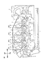
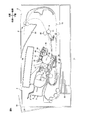
図1に示すように、画像形成装置の一例としてのプリンタ1は、横置きタイプのダイレクトタンデム型カラープリンタである。
1. Overall Configuration of Printer As shown in FIG. 1, a
なお、以下の説明において、プリンタ1の方向に言及するときには、プリンタ1を水平に載置した状態を上下の基準とする。すなわち、図1の紙面上側が上側であり、紙面下側が下側である。また、図1の紙面左側が前側であり、図1の紙面右側が後側である。また、プリンタ1を前側から見たときを左右の基準とする。すなわち、図1の紙面手前側が右側であり、紙面奥側が左側である。なお、前後方向は、第1方向の一例であり、上下方向は、第2方向の一例であり、左右方向は、第3方向の一例である。また、前側は、第1方向の一方側の一例であり、後側は、第1方向の他方側の一例である。また、上側は、第2方向の一方側の一例であり、下側は、第2方向の他方側の一例である。また、左側は、第3方向の一方側の一例であり、右側は、第3方向の他方側の一例である。
In the following description, when referring to the direction of the
プリンタ1は、略ボックス形状の本体ケーシング2を備えている。本体ケーシング2の上端部には、本体開口部3を開閉するトップカバー4が、その後端部を支点として揺動可能に設けられている。プリンタ1は、複数のプロセスユニット5と、複数のLEDユニット6と、転写ユニット7と、定着装置の一例としての定着ユニット8とを備えている。
The
すべてのプロセスユニット5は、本体ケーシング2内に着脱可能に設けられている。また、複数のプロセスユニット5は、それぞれ、イエロー、マゼンタ、シアン、ブラックのうちの1つに対応し、搬送方向の一例としての前後方向に互いに間隔を隔てて並列配置されている。具体的には、前側から後側に向かって、イエロープロセスユニット5Y、マゼンタプロセスユニット5M、シアンプロセスユニット5Cおよびブラックプロセスユニット5Kが、順次配置されている。
All the
プロセスユニット5は、ドラムユニット9と、ドラムユニット9に着脱可能に装着される現像器の一例としての現像ユニット10とを備えている。
The
ドラムユニット9は、像担持体の一例としての感光ドラム11と、帯電部材の一例としてのスコロトロン型帯電器12と、クリーニング部材の一例としてのドラムクリーニングローラ24とを備えている。
The
感光ドラム11は、長手方向の一例としての左右方向に長手の略円筒形状に形成されており、ドラムユニット9の後端部に回転可能に設けられている。なお、ブラックプロセスユニット5Kに設けられる感光ドラム11が第1像担持体の一例である。また、イエロープロセスユニット5Y、マゼンタプロセスユニット5Mおよびシアンプロセスユニット5Cのそれぞれに設けられる感光ドラム11が、第2像担持体の一例である。また、ブラックプロセスユニット5Kは、対応する転写ローラ19とともに第1画像形成ユニットを構成する。また、イエロープロセスユニット5Y、マゼンタプロセスユニット5Mおよびシアンプロセスユニット5Cのそれぞれは、対応する転写ローラ19とともに、それぞれ、第2画像形成ユニットを構成する。
The
スコロトロン型帯電器12は、感光ドラム11の後上側に間隔を隔てて対向配置されている。なお、ブラックプロセスユニット5Kに設けられるスコロトロン型帯電器12が第1帯電部材の一例である。また、イエロープロセスユニット5Y、マゼンタプロセスユニット5Mおよびシアンプロセスユニット5Cのそれぞれに設けられるスコロトロン型帯電器12が、第2帯電部材の一例である。
The
ドラムクリーニングローラ24は、感光ドラム11の後側において、スコロトロン型帯電器12の下側に配置されている。ドラムクリーニングローラ24は、感光ドラム11に対して後側から接触されている。ドラムクリーニングローラ24は、左右方向に延びる略円柱形状に形成されている。なお、ブラックプロセスユニット5Kに設けられるドラムクリーニングローラ24が第1クリーニング部材の一例である。また、イエロープロセスユニット5Y、マゼンタプロセスユニット5Mおよびシアンプロセスユニット5Cのそれぞれに設けられるドラムクリーニングローラ24が、第2クリーニング部材の一例である。
The
現像ユニット10は、現像剤担持体の一例としての現像ローラ13と、現像ローラ13にトナーを供給する供給ローラ14とを備えている。なお、ブラックプロセスユニット5Kに設けられる現像ユニット10が第1現像器の一例である。また、イエロープロセスユニット5Y、マゼンタプロセスユニット5Mおよびシアンプロセスユニット5Cのそれぞれに設けられる現像ユニット10が、第2現像器の一例である。
The developing
現像ローラ13は、現像ユニット10の後端部において、後側へ露出されるように回転可能に支持されている。現像ローラ13は、感光ドラム11に対して前上側から接触されている。現像ローラ13は、左右方向に延びる略円柱形状に形成されている。
The developing
供給ローラ14は、現像ローラ13の前上側において、現像ローラ13に接触されるように回転可能に支持されている。供給ローラ14は、左右方向に延びる略円柱形状に形成されている。
The
また、現像ユニット10は、現像ローラ13に供給されたトナーの厚みを規制する層厚規制ブレード15を備えている。また、現像ユニット10には、現像ローラ13および供給ローラ14の上側において、現像剤の一例としてのトナーが収容されている。
Further, the developing
複数のLEDユニット6のそれぞれは、複数のプロセスユニット5の感光ドラム11の上側にそれぞれ対向配置されるように、トップカバー4に支持されている。
Each of the plurality of
転写ユニット7は、複数のプロセスユニット5の下側に対向配置されている。転写ユニット7は、駆動ローラ16、従動ローラ17、搬送ベルト18、および、複数の転写部材の一例としての転写ローラ19を備えている。
The transfer unit 7 is disposed opposite to the lower side of the plurality of
駆動ローラ16は、転写ユニット7の後端部に回転可能に支持されている。
The driving
従動ローラ17は、転写ユニット7の前端部に回転可能に支持されている。
The driven
搬送ベルト18は、その上側部分がすべての感光ドラム11に下側から接触されるように、駆動ローラ16および従動ローラ17の周りに掛け渡されている。搬送ベルト18は、駆動ローラ16の駆動、および、従動ローラ17の従動により、その上側部分が前側から後側に向かって移動するように、周回移動される。
The conveying
複数の転写ローラ19のそれぞれは、複数の感光ドラム11のそれぞれの下側において、搬送ベルト18の上側部分を挟むように対向配置されている。なお、ブラックの感光ドラム11に対応する転写ローラ19が第1転写部材の一例である。また、イエロー、マゼンタおよびシアンのそれぞれの感光ドラム11に対応する転写ローラ19が、第2転写部材の一例である。
Each of the plurality of
定着ユニット8は、転写ユニット7の後側に対向配置されている。定着ユニット8は、加熱ローラ20と、加熱ローラ20に対向する加圧ローラ21とを備えている。
The fixing
そして、プリンタ1に外部のパーソナルコンピュータ51(図2参照)などから印刷ジョブが入力されると、画像形成動作が開始される。すると、現像ユニット10内のトナーは、供給ローラ14と現像ローラ13との間で正極性に摩擦帯電され、層厚規制ブレード15により、一定厚さの薄層として現像ローラ13の表面に担持される。
When a print job is input to the
一方、感光ドラム11の表面は、スコロトロン型帯電器12によって一様に正極性に帯電された後、LEDユニット6によって所定の画像データに基づいて露光される。これにより、感光ドラム11の表面には、画像データに基づく静電潜像が形成される。そして、現像ローラ13に担持されるトナーが感光ドラム11の表面上の静電潜像に供給されることにより、感光ドラム11の表面上に現像剤像の一例としてのトナー像が担持される。
On the other hand, the surface of the
転写媒体の一例としての用紙Pは、本体ケーシング2の底部に設けられる給紙トレイ22内に収容されており、各種ローラによって、後上側へUターンするように搬送されて、所定のタイミングで1枚ずつ、感光ドラム11と搬送ベルト18との間に給紙される。そして、搬送ベルト18によって、すべての感光ドラム11とすべての転写ローラ19との間を前側から後側に向かって搬送される。このとき、転写ローラ19に印加される転写バイアスにより、用紙Pにトナー像が転写される。
A sheet P as an example of a transfer medium is accommodated in a
そして、用紙Pは、加熱ローラ20と加圧ローラ21との間を通過するときに加熱および加圧される。このとき、用紙Pには、トナー像が熱定着される。
The paper P is heated and pressed when it passes between the
その後、用紙Pは、前上側へUターンするように搬送されて、トップカバー4に設けられる排紙トレイ23に排紙される。
2.プロセスユニットの詳細
(1)感光ドラム
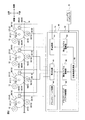
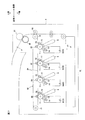
図2に示すように、感光ドラム11は、ドラム本体31とシャフト32とを備えている。
Thereafter, the paper P is conveyed so as to make a U-turn to the front upper side, and is discharged onto a
2. Details of Process Unit (1) Photosensitive Drum As shown in FIG. 2, the
ドラム本体31は、金属からなり、左右方向に延びる略円筒形状に形成されている。ドラム本体31の周面には、感光層が形成されている。ドラム本体31の左右方向両端部のそれぞれには、図示しないフランジ部材が1つずつ相対回転不能に嵌合されている。
The
シャフト32は、金属からなり、ドラム本体31の中心軸線に沿って延びる略円柱形状に形成されている。シャフト32は、図示しないフランジ部材の径方向中央を貫通するように、図示しないフランジ部材に相対回転不能に支持されている。また、シャフト32は、金属からなる図示しない導通部材を介して、ドラム本体31の内面に電気的に接続されている。また、シャフト32は、本体ケーシング2にアースされている。
(2)スコロトロン型帯電器
スコロトロン型帯電器12は、グリッド37と帯電ワイヤ38とを備えている。
The
(2) Scorotron charger The
グリッド37は、金属からなり、左右方向に延び、後上側へ向かって開放される断面視略U字形の筒形状に形成されている。
The
帯電ワイヤ38は、金属から略線形状に形成され、グリッド37内において、左右方向に沿って張架されている。
(3)転写ローラ
転写ローラ19は、転写ローラ軸33と転写ローラ本体34とを備えている。
The
(3) Transfer Roller The
転写ローラ軸33は、金属から左右方向に延びる略円柱形状に形成されている。
The
転写ローラ本体34は、導電性の樹脂材料などから、左右方向に延びる略円筒形状に形成され、転写ローラ軸33の左右方向両端部を露出するように、転写ローラ軸33を被覆している。
(4)ドラムクリーニングローラ
ドラムクリーニングローラ24は、ドラムクリーニングローラ軸35とドラムクリーニングローラ本体36とを備えている。
The
(4) Drum Cleaning Roller The
ドラムクリーニングローラ軸35は、金属からなり、左右方向に延びる略円柱形状に形成されている。
The drum cleaning
ドラムクリーニングローラ本体36は、半導電性のシリコーン樹脂やウレタン樹脂の発泡体などから形成されている。ドラムクリーニングローラ本体36は、左右方向に延びる略円筒形状に形成され、ドラムクリーニングローラ軸35の左右方向両端部を露出するように、ドラムクリーニングローラ軸35を被覆している。
3.プリンタの電気的構成
本体ケーシング2内には、制御装置の一例としての制御部40と、湿度センサ43とが設けられている。
The drum cleaning roller
3. Electrical Configuration of Printer In the
制御部40は、電源基板41と制御基板42とを備えている。
The
電源基板41は、転写ローラ19に電力を供給するための転写回路45と、ドラムクリーニングローラ24に電力を供給するためのドラムクリーニング回路46と、スコロトロン型帯電器12に電力を供給するための帯電回路47を備えている。
The
転写回路45は、配線を介して、複数の転写ローラ19のそれぞれの転写ローラ軸33に電気的に接続されている。転写回路45は、制御基板42の制御に基づいて、複数の転写ローラ19に対して、個別に、転写バイアスを印加する。
The
ドラムクリーニング回路46は、配線を介して、複数のドラムクリーニングローラ24のそれぞれのドラムクリーニングローラ軸35に電気的に接続されている。ドラムクリーニング回路46は、制御基板42の制御に基づいて、すべてのドラムクリーニングローラ24に対して、同じドラムクリーニングバイアスを印加する。
The
帯電回路47は、配線を介して、スコロトロン型帯電器12の帯電ワイヤ38に電気的に接続されている。帯電回路47は、制御基板42の制御に基づいて、イエロー、マゼンタおよびシアンのスコロトロン型帯電器12に対して、同じ帯電バイアスを印加するとともに、ブラックのスコロトロン型帯電器12に対して、個別に帯電バイアスを印加する。
The charging
制御基板42は、CPUおよびメモリなどを有している。制御基板42は、CPUによるプログラム処理によってソフトウェア的に実現される構成として、転写回路45を制御する転写バイアス制御部48と、ドラムクリーニング回路46を制御するドラムクリーニングバイアス制御部49と、帯電回路47を制御する帯電バイアス制御部50と、未使用の現像ユニット10が本体ケーシング2に装着された後において、その現像ユニット10を用いて印刷された用紙Pの枚数を計測し、記憶する印刷枚数計測部66とを備えている。
4.画像形成動作
(1)転写電流、帯電バイアスおよびドラムクリーニングバイアスの設定
上記した画像形成動作が実施されるときには、帯電バイアス制御部50において帯電バイアスが設定され、転写バイアス制御部48において転写電流が設定され、ドラムクリーニングバイアス制御部49においてドラムクリーニングバイアスが設定される。
(1−1)通常のトナー状態
印刷枚数計測部66によって計測された印刷枚数が、例えば、1500枚未満であるときには、現像ユニット10内のトナーの劣化の度合いが小さく、例えば、逆極性に帯電するトナーなどの帯電不良のトナーが発生する割合が小さいと予測される。
The
4). Image Forming Operation (1) Setting of Transfer Current, Charging Bias, and Drum Cleaning Bias When the above-described image forming operation is performed, the charging
(1-1) Normal Toner State When the number of printed sheets measured by the number-of-printed-
現像ユニット10内のトナーの劣化の度合いが小さいと予測されるときには、帯電バイアス制御部50は、すべてのスコロトロン型帯電器12に印加される帯電バイアスを、例えば、+700Vに設定する。この帯電バイアスが、第1帯電バイアスの一例である。
When it is predicted that the degree of deterioration of the toner in the developing
また、転写バイアス制御部48は、イエローの感光ドラム11と転写ローラ19の間に流す転写電流を、例えば、−8μAに設定する。
Further, the
また、転写バイアス制御部48は、マゼンタの感光ドラム11と転写ローラ19の間に流す転写電流を、例えば、−9μAに設定する。
Further, the transfer
また、転写バイアス制御部48は、シアンの感光ドラム11と転写ローラ19の間に流す転写電流を、例えば、−9μAに設定する。
Further, the
また、転写バイアス制御部48は、ブラックの感光ドラム11と転写ローラ19との間に流す転写電流を、例えば、−9μAに設定する。
Further, the transfer
また、ドラムクリーニングバイアス制御部49は、すべてのドラムクリーニングローラ24に印加されるドラムクリーニングバイアスを、例えば、−300Vに設定する。
(1−2)劣化が予想されるトナー状態
次いで、印刷枚数計測部66によって計測された印刷枚数が、例えば、1500枚以上であるときには、現像ユニット10内のトナーの劣化の度合いが大きく、帯電不良のトナーが発生する割合が大きいと予測される。
Further, the drum cleaning
(1-2) Toner State Expected to be Degraded Next, when the number of printed sheets measured by the number-of-printed-
現像ユニット10内のトナーの劣化の度合いが大きいと予測されるときには、帯電バイアス制御部50は、イエロー、マゼンタおよびシアンのスコロトロン型帯電器12に印加される帯電バイアスを、例えば、+800Vに設定する。この帯電バイアスが、第2帯電バイアスの一例である。
When the degree of deterioration of the toner in the developing
また、ブラックのスコロトロン型帯電器12に印加される帯電バイアスを、例えば、+850Vに設定する。この帯電バイアスが、第3帯電バイアスの一例である。
The charging bias applied to the
また、転写バイアス制御部48は、イエローに対応する感光ドラム11と転写ローラ19の間に流す転写電流を、例えば、−8μAに設定する。
Further, the transfer
また、転写バイアス制御部48は、マゼンタに対応する感光ドラム11と転写ローラ19の間に流す転写電流を、例えば、−9μAに設定する。
Further, the transfer
また、転写バイアス制御部48は、シアンに対応する感光ドラム11と転写ローラ19の間に流す転写電流を、例えば、−9μAに設定する。
Further, the transfer
また、転写バイアス制御部48は、ブラックに対応する感光ドラム11と転写ローラ19との間に流す転写電流を、例えば、−9μAに設定する。
Further, the
また、ドラムクリーニングバイアス制御部49は、すべてのドラムクリーニングローラ24に印加されるドラムクリーニングバイアスを、例えば、−300Vに設定する。
(2)転写・クリーニング動作
(2−1)通常のトナー状態における転写・クリーニング動作
上記した画像形成動作が実施されたときに、印刷枚数計測部66によって計測された印刷枚数が上記枚数未満であると、帯電バイアス制御部50は、帯電回路47を制御して、すべてのスコロトロン型帯電器12に、上記した帯電バイアスを印加する。
Further, the drum cleaning
(2) Transfer / cleaning operation (2-1) Transfer / cleaning operation in normal toner state When the above-described image forming operation is performed, the number of printed sheets measured by the number-of-printed-
すると、すべての感光ドラム11の表面は、LEDユニット6によって露光される前において、例えば、+700Vの帯電電位で帯電される。この帯電電位が、第1の表面電位である。
Then, the surfaces of all the
また、転写バイアス制御部48は、転写回路45を制御して、複数の転写ローラ19のそれぞれに、対応する感光ドラム11との間に上記した転写電流を一定して流すように、転写バイアスを印加する。
The
また、ドラムクリーニングバイアス制御部49は、ドラムクリーニング回路46を制御し、すべてのドラムクリーニングローラ24に、上記したドラムクリーニングバイアスを印加する。
The drum cleaning
そして、用紙Pが感光ドラム11と転写ローラ19との対向部分を通過するときに、感光ドラム11に担持されているトナー像が用紙Pに転写される。
Then, when the paper P passes through a portion where the
このとき、イエローの転写ローラ19からイエローの感光ドラム11へ転写電流が流れることにより、イエローの感光ドラム11の表面電位は、+700Vから、約+300Vに低下する。
At this time, when a transfer current flows from the
また、マゼンタの転写ローラ19からマゼンタの感光ドラム11へ転写電流が流れることにより、マゼンタの感光ドラム11の表面電位は、+700Vから、約+250Vに低下する。
Further, when a transfer current flows from the
また、シアンの転写ローラ19からシアンの感光ドラム11へ転写電流が流れることにより、シアンの感光ドラム11の表面電位は、+700Vから、約+250Vに低下する。
Further, when a transfer current flows from the
また、ブラックの転写ローラ19からブラックの感光ドラム11へ転写電流が流れることにより、ブラックの感光ドラム11の表面電位は、+700Vから、約+250Vに低下する。
Further, when a transfer current flows from the
その後、複数の感光ドラム11のそれぞれにおいて、用紙Pに転写されずに感光ドラム11の周面に残存する転写残トナーは、感光ドラム11の回転に伴って、対応するドラムクリーニングローラ24に対向され、ドラムクリーニングバイアスによって、対応するドラムクリーニングローラ24の周面に静電気的に保持される。
(2−2)劣化が予想されるトナー状態における転写・クリーニング動作
上記した画像形成動作が実施されたときに、印刷枚数計測部66によって計測された印刷枚数が上記枚数以上であると、帯電バイアス制御部50は、帯電回路47を制御して、複数のスコロトロン型帯電器12のそれぞれの帯電ワイヤ38に、上記した帯電バイアスを印加する。
Thereafter, in each of the plurality of
(2-2) Transfer / Cleaning Operation in Toner State Expected to be Degraded When the above-described image forming operation is performed, if the number of printed sheets measured by the number-of-printed-
すると、イエロー、マゼンタおよびシアンの感光ドラム11の表面は、LEDユニット6によって露光される前において、例えば、+750Vの帯電電位で帯電される。この帯電電位が、第2の表面電位である。
Then, the surface of the
また、ブラックの感光ドラム11の表面は、LEDユニット6によって露光される前において、例えば、+800Vの帯電電位で帯電される。この帯電電位が、第3の表面電位である。
Further, the surface of the black
また、転写バイアス制御部48は、転写回路45を制御して、複数の転写ローラ19のそれぞれに、対応する感光ドラム11との間に上記した転写電流を一定して流すように、転写バイアスを印加する。
The
また、ドラムクリーニングバイアス制御部49は、ドラムクリーニング回路46を制御し、すべてのドラムクリーニングローラ24に、上記したドラムクリーニングバイアスを印加する。
The drum cleaning
そして、用紙Pが感光ドラム11と転写ローラ19との対向部分を通過するときに、感光ドラム11に担持されているトナー像が用紙Pに転写される。
Then, when the paper P passes through a portion where the
このとき、イエローの転写ローラ19からイエローの感光ドラム11へ転写電流が流れることにより、イエローの感光ドラム11の表面電位は、+750Vから、約+350Vに低下する。
At this time, a transfer current flows from the
また、マゼンタの転写ローラ19からマゼンタの感光ドラム11へ転写電流が流れることにより、マゼンタの感光ドラム11の表面電位は、+750Vから、約+300Vに低下する。
Further, when a transfer current flows from the
また、シアンの転写ローラ19からシアンの感光ドラム11へ転写電流が流れることにより、シアンの感光ドラム11の表面電位は、+750Vから、約+300Vに低下する。
Further, when a transfer current flows from the
また、ブラックの転写ローラ19からブラックの感光ドラム11へ転写電流が流れることにより、ブラックの感光ドラム11の表面電位は、+800Vから、約+350Vに低下する。
Further, when a transfer current flows from the
その後、複数の感光ドラム11のそれぞれにおいて、感光ドラム11の周面に残存する転写残トナーは、上記した通常のトナー状態である場合と同様に、対応するドラムクリーニングローラ24の周面に静電気的に保持される。
4.作用効果
(1)このプリンタ1によれば、印刷枚数計測部66によって計測された印刷枚数が1500枚以上となったときに、帯電バイアスを大きくする。
Thereafter, in each of the plurality of
4). Operation and Effect (1) According to the
具体的には、イエロー、マゼンタおよびシアンの感光ドラム11に対応するスコロトロン型帯電器12に印加される帯電バイアスを+700Vから+750Vに変更する。
Specifically, the charging bias applied to the
また、ブラックの感光ドラム11に対応するスコロトロン型帯電器12に印加される帯電バイアスを+700Vから+800Vに変更する。
Further, the charging bias applied to the
これにより、印刷枚数計測部66によって計測された印刷枚数が1500枚以上となったとき、すなわち、現像ユニット10内のトナーが劣化していると予想されるときにおいて、感光ドラム11の表面電位をより大きな表面電位とする。
Thereby, when the number of printed sheets measured by the number-of-printed-
これにより、印刷枚数計測部66によって計測された印刷枚数が1500枚以上となったとき、すなわち、現像ユニット10内のトナーが劣化していると予想されるときにおいて、現像ユニット10内のトナーの劣化が少ないときと比べて、感光ドラム11の表面電位をより大きな表面電位とする。言い換えると、転写残トナーが多いと予想されるときに、転写残トナーが少ないと予想されるときに比べ、感光ドラム11の表面電位をより大きな表面電位とする。
As a result, when the number of printed sheets measured by the number-of-printed-
そのため、転写残トナーが多いと予測されるときに、感光ドラム11とドラムクリーニングローラ24との電位差を広げることができ、ドラムクリーニングローラ24に回収された転写残トナーが感光ドラム11に再付着することを抑制できる。
Therefore, when it is predicted that there is a large amount of residual toner, the potential difference between the
その結果、ドラムクリーニングローラ24によって確実に感光ドラム11をクリーニングできる。
(2)また、このプリンタ1によれば、印刷枚数計測部66によって計測された印刷枚数が1500枚以上となったときに、複数のプロセスユニット5のうち、用紙Pの搬送方向において最下流側、すなわち最後方に配置されるブラックプロセスユニット5Kのスコロトロン型帯電器12の帯電バイアスを、それよりも前側に配置されるプロセスユニット5のスコロトロン型帯電器12の帯電バイアスよりも大きくする。
As a result, the
(2) Further, according to the
その結果、特に帯電状態が変動した転写残トナーが付着しやすい最後方のブラックプロセスユニット5Kにおいて、ドラムクリーニングローラ24に回収された転写残トナーが感光ドラム11に再付着することを確実に抑制できる。
5.第2実施形態
(1)第2実施形態の概要
上記した第1実施形態では、印刷枚数計測部66によって計測された印刷枚数に基づいて、帯電バイアスを大きくしている。
As a result, it is possible to reliably prevent the transfer residual toner collected by the
5. Second Embodiment (1) Outline of Second Embodiment In the first embodiment described above, the charging bias is increased based on the number of printed sheets measured by the printed sheet
対して、第2実施形態では、1つの印刷ジョブにおいて複数枚の用紙Pに印刷する連続印刷が指定された場合に、2枚目以降の用紙に転写するときに、帯電バイアスを大きくする。なお、連続印刷される複数枚の用紙Pのうち、1枚目の用紙Pが第1の転写媒体の一例であり、2枚目以降の用紙Pが第2の転写媒体の一例である。
(2)帯電バイアスの設定
第2実施形態では、帯電バイアス制御部50は、印刷ジョブにおいて複数枚の用紙Pに対する連続印刷が指定された場合に、2枚目以降の用紙に転写するときに、上記した第1実施形態における劣化が予想されるトナー状態の場合と同様にして、複数のスコロトロン型帯電器12のそれぞれに印加する帯電バイアスを設定する。
In contrast, in the second embodiment, when continuous printing for printing on a plurality of sheets P is designated in one print job, the charging bias is increased when transferring to the second and subsequent sheets. Of the plurality of sheets P that are continuously printed, the first sheet P is an example of the first transfer medium, and the second and subsequent sheets P are examples of the second transfer medium.
(2) Setting of Charging Bias In the second embodiment, the charging
なお、帯電バイアス制御部50は、印刷ジョブにおいて1枚の用紙Pに対する印刷が指定された場合には、上記した第1実施形態における通常のトナー状態の場合と同様にして、複数のスコロトロン型帯電器12のそれぞれに印加する帯電バイアスを設定する。
(3)第2実施形態の作用効果
(3−1)複数の用紙Pに連続して印刷する場合には、ドラムクリーニングローラ24は複数の用紙Pによって感光ドラム11の表面に付着された転写残トナーを回収する。そのため、1枚の用紙Pに印刷する場合と比べて、ドラムクリーニングローラ24に保持される転写残トナーの量が多くなる。
The charging
(3) Effects of Second Embodiment (3-1) When printing on a plurality of sheets P continuously, the
このように、ドラムクリーニングローラ24に保持される転写残トナーが多くなると、ドラムクリーニングローラ24による転写残トナーの保持力が不足し、転写残トナーが感光ドラム11に再付着するおそれがある。
As described above, when the transfer residual toner held on the
しかし、第2実施形態によれば、1枚目以降の用紙Pに印刷するときに、帯電バイアスを大きくすることで、感光ドラム11とドラムクリーニングローラ24との電位差を広げることができる。
However, according to the second embodiment, the potential difference between the
その結果、ドラムクリーニングローラ24に付着した転写残トナーが感光ドラム11に再付着することを抑制できる。
(3−2)また、第2実施形態においても、上記した第1実施形態と同様の作用効果を得ることができる。
6.第3実施形態
図3を参照して、プリンタ1の第3実施形態を説明する。なお、第3実施形態において、上記した第1実施形態と同様の部材には、同じ符号を付し、その説明を省略する。
(1)第3実施形態の概要
上記した第1実施形態では、印刷枚数計測部66によって計測された印刷枚数に基づいて、帯電バイアスを大きくしている。
As a result, it is possible to prevent the transfer residual toner attached to the
(3-2) Also in the second embodiment, the same effects as those in the first embodiment can be obtained.
6). Third Embodiment A third embodiment of the
(1) Overview of Third Embodiment In the first embodiment described above, the charging bias is increased based on the number of printed sheets measured by the printed sheet
対して、第3実施形態では、本体ケーシング2内の相対湿度を湿度センサ43で検知し、検知された相対湿度に基づいて、帯電バイアスを大きくする。
(2)第3実施形態の構成
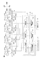
第3実施形態では、図3に示すように、本体ケーシング2内に、湿度センサ43が設けられている。
On the other hand, in the third embodiment, the relative humidity in the
(2) Configuration of Third Embodiment In the third embodiment, a
湿度センサ43は、本体ケーシング2内の相対湿度を測定するセンサであり、信号配線を介して、制御基板42に電気的に接続されている。
(3)帯電バイアスの設定
第3実施形態では、帯電バイアス制御部50は、湿度センサ43によって測定された本体ケーシング2内の相対湿度が、例えば、30%以下であるときに、上記した第1実施形態における劣化が予想されるトナー状態の場合と同様にして、複数のスコロトロン型帯電器12のそれぞれに印加する帯電バイアスを設定する。
The
(3) Setting of Charging Bias In the third embodiment, the charging
なお、帯電バイアス制御部50は、本体ケーシング2内の相対湿度が、例えば、30%超過、60%未満であるときに、上記した第1実施形態における通常のトナー状態の場合と同様にして、複数のスコロトロン型帯電器12のそれぞれに印加する帯電バイアスを設定する。
(4)第3実施形態の作用効果
(4−1)本体ケーシング2内の相対湿度が、例えば、30%以下となると、用紙Pの電気抵抗が増大し、感光ドラム11と転写ローラ19との間に印加される転写バイアスが大きくなる。この場合、用紙Pと感光ドラム11との間で放電が発生し、その放電によりトナーの帯電状態が変動する場合がある。トナーの帯電状態が変動すると、感光ドラム11から用紙Pへのトナー像の転写効率が低下し、感光ドラム11に付着する転写残トナーが増加するおそれがある。
When the relative humidity in the
(4) Effects of Third Embodiment (4-1) When the relative humidity in the
しかし、第3実施形態によれば、相対湿度が上記相対湿度以下であるときに、帯電バイアスを大きくする。 However, according to the third embodiment, the charging bias is increased when the relative humidity is equal to or lower than the relative humidity.
その結果、相対湿度が上記相対湿度以下であるときに、ドラムクリーニングローラ24に回収された転写残トナーが感光ドラム11に再付着することを抑制できる。
(4−2)また、第3実施形態においても、上記した第1実施形態と同様の作用効果を得ることができる。
7.第4実施形態
図4を参照して、プリンタ1の第4実施形態を説明する。なお、第4実施形態において、上記した第1実施形態と同様の部材には、同じ符号を付し、その説明を省略する。
(1)第4実施形態の概要
上記した第1実施形態では、印刷枚数計測部66によって計測された印刷枚数に基づいて、帯電バイアスを大きくしている。
As a result, when the relative humidity is equal to or lower than the above relative humidity, it is possible to suppress the transfer residual toner collected on the
(4-2) Also in the third embodiment, the same operational effects as those of the first embodiment described above can be obtained.
7). Fourth Embodiment A fourth embodiment of the
(1) Outline of Fourth Embodiment In the first embodiment described above, the charging bias is increased based on the number of printed sheets measured by the printed sheet
対して、第4実施形態では、転写ローラ19と感光ドラム11との間の電気抵抗を測定し、測定された電気抵抗に基づいて、帯電バイアスを大きくする。
(2)第4実施形態の構成
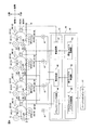
第4実施形態では、図4に示すように、電流計61と電圧計62とを備えている。
On the other hand, in the fourth embodiment, the electrical resistance between the
(2) Configuration of Fourth Embodiment In the fourth embodiment, an
電流計61は、転写回路45と転写ローラ軸33との間に介在されている。電流計61は、転写回路45から転写ローラ軸33へ流れる電流の電流値を測定する。また、電流計61は、図示しない信号配線を介して、制御基板42に電気的に接続されている。電流計61は、測定した電流値を制御基板42に送信する。
The
電圧計62は、転写ローラ軸33とシャフト32とに電気的に接続されている。電圧計62は、転写ローラ軸33とシャフト32との間に印加される電圧を測定する。また、電圧計62は、図示しない信号配線を介して、制御基板42に電気的に接続されている。電圧計62は、測定した電圧を制御基板42に送信する。
The
そして、制御基板42では、電流計61で測定された電流値と、電圧計62で測定された電圧とから転写ローラ19と感光ドラム11との間の電気抵抗を計算する。すなわち、電流計61および電圧計62は、抵抗検知部を構成する。
(3)転写電流および帯電バイアスの設定
第4実施形態では、転写ローラ19と感光ドラム11との間の電気抵抗が、例えば、500MΩ以上であるときには、帯電バイアス制御部50は、上記した第1実施形態における劣化が予想されるトナー状態の場合と同様にして、複数のスコロトロン型帯電器12のそれぞれに印加する帯電バイアスを設定する。
Then, the
(3) Setting of Transfer Current and Charging Bias In the fourth embodiment, when the electrical resistance between the
なお、転写ローラ19と感光ドラム11との間の電気抵抗が上記電気抵抗未満であるときには、帯電バイアス制御部50は、上記した第1実施形態における通常のトナー状態の場合と同様にして、複数のスコロトロン型帯電器12のそれぞれに印加する帯電バイアスを設定する。
(4)第4実施形態の作用効果
(4−1)第4実施形態によれば、用紙Pの電気抵抗を実測して、電気抵抗が高い場合に、帯電バイアスを大きくする。
When the electrical resistance between the
(4) Effects of the fourth embodiment (4-1) According to the fourth embodiment, the electrical resistance of the paper P is measured, and the charging bias is increased when the electrical resistance is high.
このように、用紙Pの実際の電気抵抗が高い場合に、感光ドラム11と転写ローラ19との間に印加される転写バイアスが大きくなる。この場合、用紙Pと感光ドラム11との間で放電が発生し、その放電によりトナーの帯電状態が変動する場合がある。トナーの帯電状態が変動すると、感光ドラム11から用紙Pへのトナー像の転写効率が低下し、感光ドラム11に付着する転写残トナーが増加するおそれがある。
Thus, when the actual electrical resistance of the paper P is high, the transfer bias applied between the
しかし、第4実施形態によれば、電気抵抗が高い場合に、帯電バイアスを大きくする。 However, according to the fourth embodiment, the charging bias is increased when the electrical resistance is high.
その結果、電気抵抗が高い場合に、ドラムクリーニングローラ24に回収された転写残トナーが感光ドラム11に再付着することを抑制できる。
(4−2)また、第4実施形態においても、上記した第1実施形態と同様の作用効果を得ることができる。
8.第5実施形態
(1)第5実施形態の概要
上記した第1実施形態では、帯電バイアス制御部50は、印刷枚数計測部66によって計測された印刷枚数に基づいて、帯電バイアスを大きくしている。
As a result, when the electrical resistance is high, it is possible to prevent the transfer residual toner collected by the
(4-2) Also in the fourth embodiment, it is possible to obtain the same operational effects as those in the first embodiment.
8). Fifth Embodiment (1) Outline of Fifth Embodiment In the first embodiment described above, the charging
対して、第5実施形態では、帯電バイアス制御部50は、外部のパーソナルコンピュータ51などからプリンタ1に1つの印刷ジョブが入力されたときに、印刷ジョブにおいて指定された用紙Pの種類に応じて、帯電バイアスを大きくする。
(2)帯電バイアスの設定
第5実施形態では、印刷ジョブにおいて指定された用紙Pの種類が、例えば、はがきなど、その左右方向長さが感光ドラム11の最大画像形成領域の左右方向長さに対して所定の割合以下となる用紙Pや、例えば、光沢紙や厚紙など、電気抵抗が比較的高い用紙Pである場合に、帯電バイアスを大きくする。
In contrast, in the fifth embodiment, when one print job is input to the
(2) Setting of Charging Bias In the fifth embodiment, the type of paper P designated in the print job is the length in the left-right direction of the maximum image forming area of the
具体的には、例えば、印刷ジョブにおいて指定された用紙Pの左右方向長さが、感光ドラム11の最大画像形成領域の左右方向長さに対して、例えば、80%以下、好ましくは、60%以下である場合に、帯電バイアス制御部50は、上記した第1実施形態における劣化が予想されるトナー状態の場合と同様にして、複数のスコロトロン型帯電器12のそれぞれに印加する帯電バイアスを設定する。
Specifically, for example, the length in the left-right direction of the sheet P designated in the print job is, for example, 80% or less, preferably 60% with respect to the length in the left-right direction of the maximum image forming area of the
なお、印刷ジョブにおいて指定された用紙Pの左右方向長さが、感光ドラム11の最大画像形成領域の左右方向長さに対して上記割合以上である場合には、帯電バイアス制御部50は、上記した第1実施形態における通常のトナー状態の場合と同様にして、複数のスコロトロン型帯電器12のそれぞれに印加する帯電バイアスを設定する。
(3)第5実施形態の作用効果
第5実施形態においても、上記した第1実施形態と同様の作用効果を得ることができる。
Note that when the horizontal length of the paper P specified in the print job is equal to or greater than the above ratio with respect to the horizontal length of the maximum image forming area of the
(3) Effects of the fifth embodiment Also in the fifth embodiment, the same functions and effects as those of the first embodiment described above can be obtained.
詳しくは、第5実施形態では、印刷ジョブにおいて指定された用紙Pが、その左右方向長さが感光ドラムの最大画像形成領域の左右方向長さに対して上記した割合以下である場合に、転写電流が感光ドラム11に流れやすくなる。そのため、トナーを用紙へ転写するための転写電流が少なくなり、感光ドラム11から用紙Pへのトナー像の転写効率が低下し、感光ドラム11に付着する転写残トナーが増加するおそれがある。
Specifically, in the fifth embodiment, when the paper P specified in the print job has a horizontal length that is equal to or less than the above-described ratio with respect to the horizontal length of the maximum image forming area of the photosensitive drum, the transfer is performed. An electric current easily flows to the
しかし、第5実施形態によれば、印刷ジョブにおいて指定された用紙Pが、その左右方向長さが感光ドラム11の最大画像形成領域の左右方向長さに対して上記した割合以下である場合に、帯電バイアスを大きくする。
However, according to the fifth embodiment, when the paper P specified in the print job has a horizontal length equal to or less than the above-described ratio with respect to the horizontal length of the maximum image forming area of the
その結果、印刷ジョブにおいて指定された用紙Pが、その左右方向長さが感光ドラム11の最大画像形成領域の左右方向長さに対して上記した割合以下である場合に、ドラムクリーニングローラ24に回収された転写残トナーが感光ドラム11に再付着することを抑制できる。
9.第6実施形態
図5を参照して、プリンタ1の第6実施形態を説明する。なお、第6実施形態において、上記した第1実施形態と同様の部材には、同じ符号を付し、その説明を省略する。
(1)第6実施形態の概要
上記した第1実施形態では、帯電回路47は、イエロー、マゼンタおよびシアンのスコロトロン型帯電器12に対して、同じ帯電バイアスを印加するとともに、ブラックのスコロトロン型帯電器12に対して、個別に帯電バイアスを印加する。
As a result, the sheet P designated in the print job is collected by the
9. Sixth Embodiment A sixth embodiment of the
(1) Outline of Sixth Embodiment In the first embodiment described above, the charging
対して、第6実施形態では、図5に示すように、帯電回路47により、複数のスコロトロン型帯電器12のそれぞれに対して、個別に、帯電バイアスを印加する。
(2)帯電バイアスの設定
第6実施形態では、印刷枚数計測部66によって計測された印刷枚数が、例えば、1500枚未満であるときには、帯電バイアス制御部50は、イエローのスコロトロン型帯電器12に印加される帯電バイアスを、例えば、+650Vに設定する。
On the other hand, in the sixth embodiment, as shown in FIG. 5, a charging bias is individually applied to each of the plurality of
(2) Setting of Charging Bias In the sixth embodiment, when the number of printed sheets measured by the printed sheet
また、帯電バイアス制御部50は、マゼンタのスコロトロン型帯電器12に印加される帯電バイアスを、例えば、+700Vに設定する。
Further, the charging
また、帯電バイアス制御部50は、シアンのスコロトロン型帯電器12に印加される帯電バイアスを、例えば、+700Vに設定する。
Further, the charging
また、帯電バイアス制御部50は、ブラックのスコロトロン型帯電器12に印加される帯電バイアスを、例えば、+700Vに設定する。
Further, the charging
また、印刷枚数計測部66によって計測された印刷枚数が、例えば、1500枚以上であるときには、帯電バイアス制御部50は、イエローのスコロトロン型帯電器12に印加される帯電バイアスを、例えば、+700Vに設定する。
Further, when the number of printed sheets measured by the printed sheet
また、帯電バイアス制御部50は、マゼンタのスコロトロン型帯電器12に印加される帯電バイアスを、例えば、+750Vに設定する。
Further, the charging
また、帯電バイアス制御部50は、シアンのスコロトロン型帯電器12に印加される帯電バイアスを、例えば、+800Vに設定する。
Further, the charging
また、帯電バイアス制御部50は、ブラックのスコロトロン型帯電器12に印加される帯電バイアスを、例えば、+800Vに設定する。
In addition, the charging
つまり、帯電バイアス制御部50は、複数のスコロトロン型帯電器12のそれぞれに印加される帯電バイアスを、より前側のスコロトロン型帯電器12に印加される帯電バイアスよりも、より後側のスコロトロン型帯電器12に印加される帯電バイアスの方が高くなるように設定する。
In other words, the charging
なお、第6実施形態では、複数の画像形成ユニットのうち、より前側に配置される画像形成ユニットが第1画像形成ユニットの一例であり、それよりも後側に配置される画像形成ユニットが第2画像形成ユニットの一例である。 In the sixth embodiment, among the plurality of image forming units, the image forming unit arranged on the front side is an example of the first image forming unit, and the image forming unit arranged on the rear side is the first image forming unit. 2 is an example of a two-image forming unit.
例えば、イエローのプロセスユニット5および転写ローラ19を第1画像形成ユニットとしたときには、それよりも後側のマゼンタ、シアンおよびブラックのプロセスユニット5のそれぞれと、それらに対応する転写ローラ19とが、第2画像形成ユニットを構成する。また、マゼンタのプロセスユニット5および転写ローラ19を第1画像形成ユニットとしたときには、それよりも後側のシアンおよびブラックのプロセスユニット5のそれぞれと、それらに対応する転写ローラ19とが、第2画像形成ユニットを構成する。また、シアンのプロセスユニット5および転写ローラ19を第1画像形成ユニットとしたときには、それよりも後側のブラックのプロセスユニット5および転写ローラ19が、第2画像形成ユニットを構成する。
For example, when the
そして、第1画像形成ユニットのプロセスユニット5に設けられる感光ドラム11が、第1像担持体の一例である。また、第1画像形成ユニットのプロセスユニット5に設けられる現像ユニット10が、第1現像器の一例である。また、第1画像形成ユニットのプロセスユニット5に設けられるスコロトロン型帯電器12が、第1帯電部材の一例である。第1画像形成ユニットのプロセスユニット5に設けられるドラムクリーニングローラ24が、第1クリーニング部材の一例である。また、第1画像形成ユニットの転写ローラ19が、第1転写部材の一例である。
The
また、第2画像形成ユニットのプロセスユニット5に設けられる感光ドラム11が、第2像担持体の一例である。また、第1画像形成ユニットのプロセスユニット5に設けられる現像ユニット10が、第1現像器の一例である。また、第2画像形成ユニットのプロセスユニット5に設けられるスコロトロン型帯電器12が、第2帯電部材の一例である。第2画像形成ユニットのプロセスユニット5に設けられるドラムクリーニングローラ24が、第2クリーニング部材の一例である。また、第2画像形成ユニットの転写ローラ19が、第2転写部材の一例である。
The
また、印刷枚数計測部66によって計測された印刷枚数が上記枚数以上である場合において、第1帯電部材に印加される帯電バイアスが第2帯電バイアスの一例であり、第2帯電部材に印加される帯電バイアスが第3帯電バイアスの一例である。
Further, when the number of printed sheets measured by the number-of-printed-
具体的には、イエローのプロセスユニット5および転写ローラ19を第1画像形成ユニットとしたときには、イエローのスコロトロン型帯電器12に印加される+700Vの帯電バイアスが第2帯電バイアスの一例であり、マゼンタのスコロトロン型帯電器12に印加される+750Vの帯電バイアス、シアンのスコロトロン型帯電器12に印加される+800Vの帯電バイアス、および、ブラックのスコロトロン型帯電器12に印加される+800Vの帯電バイアスのそれぞれが、第3帯電バイアスの一例である。また、マゼンタのプロセスユニット5および転写ローラ19を第1画像形成ユニットとしたときには、マゼンタのスコロトロン型帯電器12に印加される+750Vの帯電バイアスが第2帯電バイアスの一例であり、シアンのスコロトロン型帯電器12に印加される+800Vの帯電バイアス、および、ブラックのスコロトロン型帯電器12に印加される+800Vの帯電バイアスのそれぞれが、第3帯電バイアスの一例である。
(3)第6実施形態の作用効果
(3−1)第6実施形態においても、上記した第1実施形態と同様の作用効果を得ることができる。
10.第7実施形態
図6を参照して、プリンタ1の第7実施形態を説明する。なお、第7実施形態において、上記した第1実施形態と同様の部材には、同じ符号を付し、その説明を省略する。
(1)第7実施形態の概要
上記した第1実施形態では、プリンタ1をカラープリンタとして構成している。
Specifically, when the
(3) Operational Effects of Sixth Embodiment (3-1) In the sixth embodiment, the same operational effects as those of the first embodiment described above can be obtained.
10. Seventh Embodiment A seventh embodiment of the
(1) Overview of Seventh Embodiment In the first embodiment described above, the
対して第7実施形態では、図6に示すように、プリンタ71をモノクロプリンタとして構成する。
(2)第7実施形態の構成
第7実施形態のプリンタ71は、イエロー、マゼンタ、シアンのプロセスユニット5を有さず、ブラックのプロセスユニット5を有する。
On the other hand, in the seventh embodiment, as shown in FIG. 6, the
(2) Configuration of the Seventh Embodiment The
また、第7実施形態のプリンタ71は、転写ユニット7を有さず、代わりに、転写部材の一例としての転写ローラ72を有する。
Further, the
転写ローラ72は、プロセスユニット5の後端部において、感光ドラム11の下側に回転可能に支持されている。転写ローラ72は、感光ドラム11に対して下側から接触されている。
The
また、第7実施形態のプリンタ71には、図6中に仮想線で示すように、トナー像が定着された用紙Pを、定着ユニット8から、感光ドラム11と転写ローラ72との間へ搬送する搬送手段の一例としての反転パス73が設けられている。
In the
反転パス73は、定着ユニット8の後方を上下方向に延び、その後、給紙トレイ22の上側、かつ、定着ユニット8およびプロセスユニット5の下側を、前後方向に延びるように設けられている。反転パス73の前端部は、プロセスユニット5の前後方向略中央部に臨んでいる。また、反転パス73の後端部は、用紙Pを排紙するための排紙ローラ74の後下側に対向配置されている。
The
トナー像が定着された用紙Pは、排紙トレイ23に排紙される前に、排紙ローラ74の回転により、トナー像が定着された第1の面が下側を向くように、反転パス73内に導入される。
Before the paper P on which the toner image is fixed is discharged to the
その後、用紙Pは、反転パス73を後側から前側へ通過して、トナー像が定着された第1の面と反対側の第2の面が上側を向くように、感光ドラム11と転写ローラ72との間へ供給される。
Thereafter, the sheet P passes through the
なお、第7実施形態のプリンタ71では、本体開口部3は、本体ケーシング2の前端部に形成されており、本体ケーシング2の前端部には、本体開口部3を開閉するフロントカバー75が、その下端部を支点として揺動可能に設けられている。
In the
また、第7実施形態のプリンタ71では、スキャナユニット76によって、感光ドラム11が露光される。スキャナユニット76は、プロセスユニット5の上側に対向配置されている。スキャナユニット76は、実線で示すように、感光ドラム11に向けて、画像データに基づいて、レーザービームを出射する。
(3)帯電バイアスの設定
第7実施形態では、印刷枚数計測部66によって計測された印刷枚数が、例えば、1500枚未満であるときには、帯電バイアス制御部50は、スコロトロン型帯電器12に印加される帯電バイアスを、例えば、+700Vに設定する。この帯電バイアスが、第1帯電バイアスの一例である。
In the
(3) Setting of Charging Bias In the seventh embodiment, the charging
また、転写バイアス制御部48は、感光ドラム11と転写ローラ72との間に流す転写電流を、例えば、−9μAに設定する。
Further, the
また、印刷枚数計測部66によって計測された印刷枚数が、例えば、1500枚以上であるときには、帯電バイアス制御部50は、スコロトロン型帯電器12に印加される帯電バイアスを、例えば、+800Vに設定する。この帯電バイアスが、第2帯電バイアスの一例である。
Further, when the number of printed sheets measured by the printed sheet
また、転写バイアス制御部48は、感光ドラム11と転写ローラ72との間に流す転写電流を、例えば、−9μAに設定する。
Further, the
なお、第7実施形態では、転写バイアス制御部48および帯電バイアス制御部50は、外部のパーソナルコンピュータ51などからプリンタ1に印刷ジョブが入力されたときに、印刷ジョブにおいて、両面印刷が指定された場合、すなわち、用紙Pの両面に連続して印刷する場合に、トナー像が定着された第1の面と反対側の第2の面に転写するときに、帯電バイアスを大きくすることもできる。
In the seventh embodiment, the transfer
具体的には、第1の面に転写するときには、帯電バイアス制御部50は、スコロトロン型帯電器12に印加される帯電バイアスを、例えば、+700Vに設定する。この帯電バイアスが、第1帯電バイアスの一例である。
Specifically, when transferring to the first surface, the charging
また、転写バイアス制御部48は、感光ドラム11と転写ローラ72との間に印加する転写バイアスを、例えば、−1350Vに設定する。
Further, the
また、第2の面に転写するときには、帯電バイアス制御部50は、スコロトロン型帯電器12に印加される帯電バイアスを、例えば、+800Vに設定する。この帯電バイアスが、第2帯電バイアスの一例である。
Further, when transferring to the second surface, the charging
また、転写バイアス制御部48は、感光ドラム11と転写ローラ72との間に印加する転写バイアスを、例えば、−4500Vに設定する。
(4)第7実施形態の作用効果
(4−1)第7実施形態のプリンタ71では、定着ユニット8を通過して加熱されることにより、用紙Pが乾燥されて、その電気抵抗が高くなっている場合であっても、裏面、すなわち、第2の面を印字するときに帯電バイアスを大きくする。そのため、感光ドラム11とドラムクリーニングローラ24との電位差を広げることができ、ドラムクリーニングローラ24に回収された転写残トナーが感光ドラム11に再付着することを抑制できる。
(4−2)また、第7実施形態においても、上記した第1実施形態と同様の作用効果を得ることができる。
11.第8実施形態
図7を参照して、プリンタ1の第8実施形態を説明する。なお、第8実施形態において、上記した第1実施形態と同様の部材には、同じ符号を付し、その説明を省略する。
(1)第8実施形態の概要
上記した第1実施形態では、プリンタ1をダイレクトタンデム型のカラープリンタとして構成している。
Further, the
(4) Effects of the Seventh Embodiment (4-1) In the
(4-2) Also in the seventh embodiment, the same operational effects as those of the first embodiment described above can be obtained.
11. Eighth Embodiment With reference to FIG. 7, an eighth embodiment of the
(1) Overview of Eighth Embodiment In the first embodiment described above, the
対して第8実施形態では、図7に示すように、プリンタ81を中間転写型のカラープリンタとして構成する。
(2)第8実施形態の構成
第8実施形態のプリンタ81では、スコロトロン型帯電器12は、感光ドラム11の後下側に間隔を隔てて配置されている。
On the other hand, in the eighth embodiment, as shown in FIG. 7, the
(2) Configuration of the Eighth Embodiment In the
また、ドラムクリーニングローラ24は、感光ドラム11の後側において、スコロトロン型帯電器12の上側に配置されている。
The
また、現像ユニット10は、感光ドラム11の前下側に配置されている。
Further, the developing
現像ローラ13は、現像ユニット10の上端において、上側へ露出されるように回転可能に支持されており、感光ドラム11に対して前下側から接触されている。
The developing
供給ローラ14は、現像ローラ13の前下側において、現像ローラ13に接触されるように回転可能に支持されている。
The
また、転写ユニット7は、複数のプロセスユニット5の上側に対向配置されている。転写ユニット7は、ベルトユニット82と、二次転写ローラ83とを備えている。
Further, the transfer unit 7 is disposed to face the upper side of the plurality of
ベルトユニット82は、駆動ローラ16、従動ローラ17、転写媒体の一例としての中間転写ベルト84、および、複数の転写部材の一例としての一次転写ローラ85を備えている。
The
駆動ローラ16は、ベルトユニット82の後端部に回転可能に支持されている。
The driving
従動ローラ17は、ベルトユニット82の前端部に回転可能に支持されている。
The driven
中間転写ベルト84は、その上側部分がすべての感光ドラム11に下側から接触されるように、駆動ローラ16および従動ローラ17の周りに掛け渡されている。中間転写ベルト84は、駆動ローラ16の駆動、および、従動ローラ17の従動により、その下側部分が前側から後側に向かって移動するように、周回移動される。
The
複数の一次転写ローラ85のそれぞれは、複数の感光ドラム11のそれぞれの上側において、中間転写ベルト84の下側部分を挟むように対向配置されている。なお、ブラックの感光ドラム11に対応する一次転写ローラ85が、第1転写部材の一例である。また、イエロー、マゼンタおよびシアンのそれぞれの感光ドラム11に対応する一次転写ローラ85が、第2転写部材の一例である。
(3)第8実施形態の画像形成動作
プリンタ1に印刷ジョブが入力されると、現像ユニット10内のトナーは、供給ローラ14と現像ローラ13との間で摩擦帯電され、一定厚さの薄層として現像ローラ13の表面に担持される。
Each of the plurality of
(3) Image Forming Operation of Eighth Embodiment When a print job is input to the
一方、感光ドラム11の表面は、スコロトロン型帯電器12によって一様に帯電された後、LEDユニット6によって所定の画像データに基づいて露光される。これにより、感光ドラム11の表面には、画像データに基づく静電潜像が形成される。そして、現像ローラ13に担持されるトナーが感光ドラム11の表面上の静電潜像に供給されることにより、感光ドラム11の表面上にトナー像が担持される。
On the other hand, the surface of the
感光ドラム11の表面に担持されたトナー像は、中間転写ベルト84の下側部分に順次、転写される。これにより、中間転写ベルト84の表面にカラー画像が形成される。
The toner images carried on the surface of the
用紙Pは、本体ケーシング2の底部に設けられる給紙トレイ22内に収容されており、各種ローラによって、後上側へ搬送されて、所定のタイミングで1枚ずつ、中間転写ベルト84と二次転写ローラ83との間に給紙され、中間転写ベルト84と二次転写ローラ83との間を下側から上側に向かって通過される。このとき、用紙Pにカラー画像が転写される。
The paper P is accommodated in a
そして、用紙Pは、加熱ローラ20と加圧ローラ21との間を通過するときに加熱および加圧される。このとき、用紙Pには、カラー画像が熱定着される。その後、用紙Pは、排紙トレイ23に排紙される。
(4)転写電流および帯電バイアスの設定
第7実施形態では、帯電バイアス制御部50は、上記した第1実施形態と同様にして、複数のスコロトロン型帯電器12のそれぞれに印加する帯電バイアスを設定する。
The paper P is heated and pressed when it passes between the
(4) Setting of Transfer Current and Charging Bias In the seventh embodiment, the charging
また、転写バイアス制御部48は、上記した第1実施形態と同様にして、複数の感光ドラム11のそれぞれと、対応する一次転写ローラ85との間に流す転写電流を設定する。
(5)第8実施形態の作用効果
第8実施形態においても、上記した第1実施形態と同様の作用効果を得ることができる。
12.変形例
(1)上記した各実施形態では、制御基板42は、CPUを備えているが、例えば、CPUの代わりに、ASIC、すなわち特定用途向け集積回路を備えていてもよい。
(2)上記した各実施形態において、感光ドラム11に付着する転写残トナーを、現像ローラ13で回収するように構成してもよい。
The
(5) Effects of the Eighth Embodiment Also in the eighth embodiment, the same functions and effects as those of the first embodiment described above can be obtained.
12 Modification (1) In each of the above-described embodiments, the
(2) In each of the embodiments described above, the transfer residual toner adhering to the
この変形例では、感光ドラム11の表面電位が転写電流によって低下することが抑制された状態で、感光ドラム11に付着している転写残トナーを、ドラムクリーニングローラ24および現像ローラ13によって、より確実にクリーニングできる。
(3)上記した第1実施形態では、印刷枚数計測部66によって計測された印刷枚数が所定の枚数以上となったときに、帯電バイアスを大きくしたが、例えば、現像ローラ13の回転数が所定の回転数以上となったときや、画像形成前に印刷テストを実施し、印刷画像の濃度が所定の濃度以下となったときに、帯電バイアスを大きくすることもできる。
(4)上記した各実施形態は、互いに組み合わせて実施することもできる。
In this modification, the transfer residual toner adhering to the
(3) In the first embodiment described above, the charging bias is increased when the number of printed sheets measured by the printed sheet
(4) Each above-mentioned embodiment can also be implemented in combination with each other.
例えば、第1実施形態、第2実施形態、第3実施形態、第4実施形態および第5実施形態は、互いに組み合わせて実施することができる。 For example, 1st Embodiment, 2nd Embodiment, 3rd Embodiment, 4th Embodiment, and 5th Embodiment can be implemented in combination with each other.
また、例えば、第7実施形態および第8実施形態において、上記した第1実施形態、第2実施形態、第3実施形態、第4実施形態および第5実施形態の少なくとも1つを適用することもできる。 For example, in the seventh embodiment and the eighth embodiment, at least one of the first embodiment, the second embodiment, the third embodiment, the fourth embodiment, and the fifth embodiment described above may be applied. it can.
また、例えば、第8実施形態に上記した第6実施形態を適用することもできる。 For example, the sixth embodiment described above can be applied to the eighth embodiment.
1 プリンタ
5 プロセスユニット
11 感光ドラム
12 スコロトロン型帯電器
13 現像ローラ
19 転写ローラ
24 ドラムクリーニングローラ
40 制御部
43 湿度センサ
61 電流計
62 電圧計
66 印刷枚数計測部
71 プリンタ
72 転写ローラ
81 プリンタ
84 中間転写ベルト
85 一次転写ローラ
P 用紙
DESCRIPTION OF
Claims (11)
前記帯電部材に印加される帯電バイアスを制御するように構成される制御装置と
を備え、
前記制御装置は、
前記像担持体に付着している転写残トナーが比較的少ないときに、前記像担持体の表面電位が第1の表面電位となるように前記帯電部材に第1帯電バイアスを印加し、
前記像担持体に付着している転写残トナーが比較的多いときに、前記像担持体の表面電位が前記第1の表面電位よりも大きな第2の表面電位となるように前記帯電部材に第2帯電バイアスを印加する
ことを特徴とする、画像形成装置。 An image carrier capable of carrying a developer image, a charging member configured to charge the surface of the image carrier, a developer configured to supply developer to the image carrier, and development A transfer member configured to transfer an agent image from the image carrier to a transfer medium, and cleaning residual toner adhering to the image carrier after the developer image is transferred to the transfer medium. An image forming unit having a cleaning member constituted by:
A controller configured to control a charging bias applied to the charging member;
The control device includes:
Applying a first charging bias to the charging member such that the surface potential of the image carrier becomes a first surface potential when the transfer residual toner adhering to the image carrier is relatively small;
When the transfer residual toner adhering to the image carrier is relatively large, the charging member has a second surface potential that is higher than the first surface potential. An image forming apparatus, wherein two charging biases are applied.
ことを特徴とする、請求項1に記載の画像形成装置。 The control device is configured to detect the deterioration of the developer in the developing unit, and when the deterioration of the developer in the developing unit is detected, the surface potential of the image carrier is set to the second surface. The image forming apparatus according to claim 1, wherein the second charging bias is applied to the charging member so as to have a potential.
前記第1の転写媒体に印刷するときに、前記像担持体の表面電位が前記第1の表面電位となるように前記帯電部材に前記第1帯電バイアスを印加し、
前記第2の転写媒体に印刷するときに、前記像担持体の表面電位が前記第2の表面電位となるように前記帯電部材に前記第2帯電バイアスを印加する
ことを特徴とする、請求項1に記載の画像形成装置。 When the controller continuously prints in this order on the first transfer medium and the second transfer medium,
When printing on the first transfer medium, applying the first charging bias to the charging member so that the surface potential of the image carrier becomes the first surface potential;
The second charging bias is applied to the charging member so that a surface potential of the image carrier becomes the second surface potential when printing on the second transfer medium. The image forming apparatus according to 1.
現像剤像が前記第1の面に定着された転写媒体を、前記定着装置から前記像担持体と前記転写部材との間へ搬送するように構成される搬送手段と
を、さらに備え、
前記制御装置は、前記搬送手段によって搬送された転写媒体の前記第1の面と反対側の第2の面に現像剤像を転写する場合に、前記像担持体の表面電位が前記第2の表面電位となるように前記帯電部材に前記第2帯電バイアスを印加する
ことを特徴とする、請求項1に記載の画像形成装置。 A fixing device that heats a transfer medium having a developer image transferred to a first surface and fixes the developer image on the first surface;
A transport unit configured to transport the transfer medium having the developer image fixed on the first surface from the fixing device to between the image carrier and the transfer member;
When transferring the developer image to the second surface opposite to the first surface of the transfer medium conveyed by the conveying means, the control device determines that the surface potential of the image carrier is the second potential. The image forming apparatus according to claim 1, wherein the second charging bias is applied to the charging member so as to have a surface potential.
前記制御装置は、前記湿度センサに測定された相対湿度が所定の相対湿度以下であるときに、前記像担持体の表面電位が前記第2の表面電位となるように前記帯電部材に前記第2帯電バイアスを印加する
ことを特徴とする、請求項1に記載の画像形成装置。 Further comprising a humidity sensor configured to measure relative humidity;
When the relative humidity measured by the humidity sensor is equal to or lower than a predetermined relative humidity, the control device causes the charging member to apply the second surface potential to the second charging member so that the surface potential of the image carrier becomes the second surface potential. The image forming apparatus according to claim 1, wherein a charging bias is applied.
前記制御装置は、前記抵抗検知部に測定された電気抵抗が所定の電気抵抗以上であるときに、前記像担持体の表面電位が前記第2の表面電位となるように前記帯電部材に前記第2帯電バイアスを印加する
ことを特徴とする、請求項1に記載の画像形成装置。 A resistance detector configured to measure the electrical resistance of the transfer medium, further comprising:
The controller controls the charging member so that the surface potential of the image carrier becomes the second surface potential when the electrical resistance measured by the resistance detector is equal to or higher than a predetermined electrical resistance. The image forming apparatus according to claim 1, wherein two charging biases are applied.
ことを特徴とする、請求項1に記載の画像形成装置。 The control device applies the second charging bias to the charging member so that the surface potential of the image carrier becomes the second surface potential when printing on a predetermined type of transfer medium. The image forming apparatus according to claim 1.
ことを特徴とする、請求項7に記載の画像形成装置。 When the length of the transfer medium in the longitudinal direction of the image carrier is equal to or less than a predetermined ratio with respect to the maximum image forming area of the image carrier, the controller is configured such that the surface potential of the image carrier is The image forming apparatus according to claim 7, wherein the second charging bias is applied to the charging member so as to have a second surface potential.
前記現像剤担持体は、前記像担持体に付着する転写残トナーを回収するように構成されている
ことを特徴とする、請求項1ないし8のいずれか一項に記載の画像形成装置。 The image forming unit is further configured to support a developer, and further includes a developer carrier configured to supply the developer to the image carrier.
9. The image forming apparatus according to claim 1, wherein the developer carrying member is configured to collect a transfer residual toner attached to the image carrying member.
前記第1画像形成ユニットは、現像剤像を担持可能な第1像担持体と、前記第1像担持体の表面を帯電するように構成される第1帯電部材と、前記第1像担持体に現像剤を供給するように構成される第1現像器と、現像剤像を前記第1像担持体から転写媒体に転写するように構成される第1転写部材と、現像剤像が転写媒体に転写された後に、前記第1像担持体に付着している転写残トナーをクリーニングするように構成される第1クリーニング部材とを備え、
前記第2画像形成ユニットは、現像剤像を担持可能な第2像担持体と、前記第2像担持体の表面を帯電するように構成される第2帯電部材と、前記第2像担持体に現像剤を供給するように構成される第2現像器と、現像剤像を前記第2像担持体から転写媒体に転写するように構成される第2転写部材と、現像剤像が転写媒体に転写された後に、前記第2像担持体に付着している転写残トナーをクリーニングするように構成される第2クリーニング部材とを備え、
前記制御装置は、
前記第1帯電部材および前記第2帯電部材のそれぞれに印加される帯電バイアスを制御するように構成され、
前記第1像担持体の表面電位が前記第2の表面電位となるように前記第1帯電部材に前記第2帯電バイアスを印加するときに、前記第2像担持体の表面電位が前記第2の表面電位よりも大きな第3の表面電位となるように前記第2帯電部材に第3帯電バイアスを印加する
ことを特徴とする、請求項1ないし9のいずれか一項に記載の画像形成装置。 The image forming unit includes a first image forming unit and a second image forming unit disposed on the downstream side of the first image forming unit in the transfer direction of the transfer medium,
The first image forming unit includes a first image carrier capable of carrying a developer image, a first charging member configured to charge a surface of the first image carrier, and the first image carrier. A first developer configured to supply developer to the first transfer member, a first transfer member configured to transfer the developer image from the first image carrier to a transfer medium, and the developer image as a transfer medium. A first cleaning member configured to clean transfer residual toner attached to the first image carrier after being transferred to the first image carrier,
The second image forming unit includes a second image carrier capable of carrying a developer image, a second charging member configured to charge a surface of the second image carrier, and the second image carrier. A second developer configured to supply developer to the second transfer member, a second transfer member configured to transfer the developer image from the second image carrier to a transfer medium, and the developer image as a transfer medium. A second cleaning member configured to clean transfer residual toner adhering to the second image carrier after being transferred to the second image carrier,
The control device includes:
Configured to control a charging bias applied to each of the first charging member and the second charging member;
When the second charging bias is applied to the first charging member so that the surface potential of the first image carrier becomes the second surface potential, the surface potential of the second image carrier is the second surface potential. 10. The image forming apparatus according to claim 1, wherein a third charging bias is applied to the second charging member so as to have a third surface potential larger than the surface potential of the image forming apparatus. .
前記第1画像形成ユニットは、現像剤像を担持可能な第1像担持体と、前記第1像担持体の表面を帯電するように構成される第1帯電部材と、前記第1像担持体に現像剤を供給するように構成される第1現像器と、現像剤像を前記第1像担持体から転写媒体に転写するように構成される第1転写部材と、現像剤像が転写媒体に転写された後に、前記第1像担持体に付着している転写残トナーをクリーニングするように構成される第1クリーニング部材とを備え、
前記第2画像形成ユニットは、現像剤像を担持可能な第2像担持体と、前記第2像担持体の表面を帯電するように構成される第2帯電部材と、前記第2像担持体に現像剤を供給するように構成される第2現像器と、現像剤像を前記第2像担持体から転写媒体に転写するように構成される第2転写部材と、現像剤像が転写媒体に転写された後に、前記第2像担持体に付着している転写残トナーをクリーニングするように構成される第2クリーニング部材とを備え、
前記制御装置は、前記第2像担持体の表面電位が前記第2の表面電位となるように前記第2帯電部材に前記第2帯電バイアスを印加するときに、前記第1像担持体の表面電位が前記第2の表面電位よりも大きな第3の表面電位となるように前記第1帯電部材に第3帯電バイアスを印加する
ことを特徴とする、請求項1ないし9のいずれか一項に記載の画像形成装置。 A plurality of the image forming units are provided, a first image forming unit disposed on the most downstream side in the transport direction of the transfer medium, and a second image disposed on the upstream side in the transport direction with respect to the first image forming unit. An image forming unit,
The first image forming unit includes a first image carrier capable of carrying a developer image, a first charging member configured to charge a surface of the first image carrier, and the first image carrier. A first developer configured to supply developer to the first transfer member, a first transfer member configured to transfer the developer image from the first image carrier to a transfer medium, and the developer image as a transfer medium. A first cleaning member configured to clean transfer residual toner attached to the first image carrier after being transferred to the first image carrier,
The second image forming unit includes a second image carrier capable of carrying a developer image, a second charging member configured to charge a surface of the second image carrier, and the second image carrier. A second developer configured to supply developer to the second transfer member, a second transfer member configured to transfer the developer image from the second image carrier to a transfer medium, and the developer image as a transfer medium. A second cleaning member configured to clean transfer residual toner adhering to the second image carrier after being transferred to the second image carrier,
The controller controls the surface of the first image carrier when applying the second charging bias to the second charging member so that the surface potential of the second image carrier becomes the second surface potential. 10. The third charging bias is applied to the first charging member so that the potential becomes a third surface potential larger than the second surface potential. 10. The image forming apparatus described.
Priority Applications (1)
| Application Number | Priority Date | Filing Date | Title |
|---|---|---|---|
| JP2013017860A JP2014149403A (en) | 2013-01-31 | 2013-01-31 | Image forming apparatus |
Applications Claiming Priority (1)
| Application Number | Priority Date | Filing Date | Title |
|---|---|---|---|
| JP2013017860A JP2014149403A (en) | 2013-01-31 | 2013-01-31 | Image forming apparatus |
Publications (1)
| Publication Number | Publication Date |
|---|---|
| JP2014149403A true JP2014149403A (en) | 2014-08-21 |
Family
ID=51572423
Family Applications (1)
| Application Number | Title | Priority Date | Filing Date |
|---|---|---|---|
| JP2013017860A Pending JP2014149403A (en) | 2013-01-31 | 2013-01-31 | Image forming apparatus |
Country Status (1)
| Country | Link |
|---|---|
| JP (1) | JP2014149403A (en) |
-
2013
- 2013-01-31 JP JP2013017860A patent/JP2014149403A/en active Pending
Similar Documents
| Publication | Publication Date | Title |
|---|---|---|
| US8045875B2 (en) | Image forming apparatus and image forming method capable of generating stable transfer electric field | |
| US9046829B2 (en) | Image formation apparatus that adjusts density of current flowing through a recording medium | |
| JP4027287B2 (en) | Image forming apparatus | |
| JP2009265604A (en) | Image forming method and image forming apparatus | |
| US9031430B2 (en) | Image forming apparatus | |
| US20140056604A1 (en) | Image Forming Apparatus | |
| JP6107183B2 (en) | Image forming apparatus | |
| JP4487621B2 (en) | Transfer device and image forming apparatus having the same | |
| JP5115589B2 (en) | Image forming apparatus | |
| CN102608896A (en) | Image forming apparatus and image forming method | |
| JP2012203178A (en) | Image forming apparatus | |
| US8774658B2 (en) | Image forming apparatus including control unit that executes energy control by controlling biases | |
| JP2010151943A (en) | Color image forming apparatus and color image forming method | |
| JP6107034B2 (en) | Image forming apparatus | |
| JP4059012B2 (en) | Image forming apparatus | |
| JP4246463B2 (en) | TRANSFER METHOD, TRANSFER DEVICE, IMAGE FORMING METHOD, AND IMAGE FORMING DEVICE | |
| JP2010072249A (en) | Image-forming device | |
| JP4019613B2 (en) | Image forming apparatus | |
| JP2014149403A (en) | Image forming apparatus | |
| JP6679253B2 (en) | Image forming device | |
| JP2005148281A (en) | Image forming apparatus | |
| JP2006138891A (en) | Image forming apparatus | |
| JP2007171540A (en) | Image forming apparatus | |
| JP2013092734A (en) | Image forming apparatus | |
| JP5317497B2 (en) | Image forming apparatus |