JP2014182203A - 表示装置および電子機器 - Google Patents
表示装置および電子機器 Download PDFInfo
- Publication number
- JP2014182203A JP2014182203A JP2013055243A JP2013055243A JP2014182203A JP 2014182203 A JP2014182203 A JP 2014182203A JP 2013055243 A JP2013055243 A JP 2013055243A JP 2013055243 A JP2013055243 A JP 2013055243A JP 2014182203 A JP2014182203 A JP 2014182203A
- Authority
- JP
- Japan
- Prior art keywords
- signal
- potential
- transfer circuit
- display device
- shift
- Prior art date
- Legal status (The legal status is an assumption and is not a legal conclusion. Google has not performed a legal analysis and makes no representation as to the accuracy of the status listed.)
- Pending
Links
Images











Classifications
-
- G—PHYSICS
- G06—COMPUTING OR CALCULATING; COUNTING
- G06F—ELECTRIC DIGITAL DATA PROCESSING
- G06F3/00—Input arrangements for transferring data to be processed into a form capable of being handled by the computer; Output arrangements for transferring data from processing unit to output unit, e.g. interface arrangements
- G06F3/01—Input arrangements or combined input and output arrangements for interaction between user and computer
- G06F3/03—Arrangements for converting the position or the displacement of a member into a coded form
- G06F3/041—Digitisers, e.g. for touch screens or touch pads, characterised by the transducing means
- G06F3/0416—Control or interface arrangements specially adapted for digitisers
- G06F3/04166—Details of scanning methods, e.g. sampling time, grouping of sub areas or time sharing with display driving
-
- G—PHYSICS
- G02—OPTICS
- G02F—OPTICAL DEVICES OR ARRANGEMENTS FOR THE CONTROL OF LIGHT BY MODIFICATION OF THE OPTICAL PROPERTIES OF THE MEDIA OF THE ELEMENTS INVOLVED THEREIN; NON-LINEAR OPTICS; FREQUENCY-CHANGING OF LIGHT; OPTICAL LOGIC ELEMENTS; OPTICAL ANALOGUE/DIGITAL CONVERTERS
- G02F1/00—Devices or arrangements for the control of the intensity, colour, phase, polarisation or direction of light arriving from an independent light source, e.g. switching, gating or modulating; Non-linear optics
- G02F1/01—Devices or arrangements for the control of the intensity, colour, phase, polarisation or direction of light arriving from an independent light source, e.g. switching, gating or modulating; Non-linear optics for the control of the intensity, phase, polarisation or colour
- G02F1/13—Devices or arrangements for the control of the intensity, colour, phase, polarisation or direction of light arriving from an independent light source, e.g. switching, gating or modulating; Non-linear optics for the control of the intensity, phase, polarisation or colour based on liquid crystals, e.g. single liquid crystal display cells
- G02F1/133—Constructional arrangements; Operation of liquid crystal cells; Circuit arrangements
- G02F1/1333—Constructional arrangements; Manufacturing methods
- G02F1/13338—Input devices, e.g. touch panels
-
- G—PHYSICS
- G06—COMPUTING OR CALCULATING; COUNTING
- G06F—ELECTRIC DIGITAL DATA PROCESSING
- G06F3/00—Input arrangements for transferring data to be processed into a form capable of being handled by the computer; Output arrangements for transferring data from processing unit to output unit, e.g. interface arrangements
- G06F3/01—Input arrangements or combined input and output arrangements for interaction between user and computer
- G06F3/03—Arrangements for converting the position or the displacement of a member into a coded form
- G06F3/041—Digitisers, e.g. for touch screens or touch pads, characterised by the transducing means
- G06F3/0412—Digitisers structurally integrated in a display
-
- G—PHYSICS
- G06—COMPUTING OR CALCULATING; COUNTING
- G06F—ELECTRIC DIGITAL DATA PROCESSING
- G06F3/00—Input arrangements for transferring data to be processed into a form capable of being handled by the computer; Output arrangements for transferring data from processing unit to output unit, e.g. interface arrangements
- G06F3/01—Input arrangements or combined input and output arrangements for interaction between user and computer
- G06F3/03—Arrangements for converting the position or the displacement of a member into a coded form
- G06F3/041—Digitisers, e.g. for touch screens or touch pads, characterised by the transducing means
- G06F3/0416—Control or interface arrangements specially adapted for digitisers
- G06F3/0418—Control or interface arrangements specially adapted for digitisers for error correction or compensation, e.g. based on parallax, calibration or alignment
- G06F3/04184—Synchronisation with the driving of the display or the backlighting unit to avoid interferences generated internally
-
- G—PHYSICS
- G06—COMPUTING OR CALCULATING; COUNTING
- G06F—ELECTRIC DIGITAL DATA PROCESSING
- G06F3/00—Input arrangements for transferring data to be processed into a form capable of being handled by the computer; Output arrangements for transferring data from processing unit to output unit, e.g. interface arrangements
- G06F3/01—Input arrangements or combined input and output arrangements for interaction between user and computer
- G06F3/03—Arrangements for converting the position or the displacement of a member into a coded form
- G06F3/041—Digitisers, e.g. for touch screens or touch pads, characterised by the transducing means
- G06F3/044—Digitisers, e.g. for touch screens or touch pads, characterised by the transducing means by capacitive means
- G06F3/0445—Digitisers, e.g. for touch screens or touch pads, characterised by the transducing means by capacitive means using two or more layers of sensing electrodes, e.g. using two layers of electrodes separated by a dielectric layer
-
- G—PHYSICS
- G06—COMPUTING OR CALCULATING; COUNTING
- G06F—ELECTRIC DIGITAL DATA PROCESSING
- G06F3/00—Input arrangements for transferring data to be processed into a form capable of being handled by the computer; Output arrangements for transferring data from processing unit to output unit, e.g. interface arrangements
- G06F3/01—Input arrangements or combined input and output arrangements for interaction between user and computer
- G06F3/03—Arrangements for converting the position or the displacement of a member into a coded form
- G06F3/041—Digitisers, e.g. for touch screens or touch pads, characterised by the transducing means
- G06F3/044—Digitisers, e.g. for touch screens or touch pads, characterised by the transducing means by capacitive means
- G06F3/0446—Digitisers, e.g. for touch screens or touch pads, characterised by the transducing means by capacitive means using a grid-like structure of electrodes in at least two directions, e.g. using row and column electrodes
-
- G—PHYSICS
- G09—EDUCATION; CRYPTOGRAPHY; DISPLAY; ADVERTISING; SEALS
- G09G—ARRANGEMENTS OR CIRCUITS FOR CONTROL OF INDICATING DEVICES USING STATIC MEANS TO PRESENT VARIABLE INFORMATION
- G09G3/00—Control arrangements or circuits, of interest only in connection with visual indicators other than cathode-ray tubes
- G09G3/20—Control arrangements or circuits, of interest only in connection with visual indicators other than cathode-ray tubes for presentation of an assembly of a number of characters, e.g. a page, by composing the assembly by combination of individual elements arranged in a matrix no fixed position being assigned to or needed to be assigned to the individual characters or partial characters
- G09G3/2092—Details of a display terminals using a flat panel, the details relating to the control arrangement of the display terminal and to the interfaces thereto
-
- G—PHYSICS
- G11—INFORMATION STORAGE
- G11C—STATIC STORES
- G11C19/00—Digital stores in which the information is moved stepwise, e.g. shift registers
- G11C19/18—Digital stores in which the information is moved stepwise, e.g. shift registers using capacitors as main elements of the stages
- G11C19/182—Digital stores in which the information is moved stepwise, e.g. shift registers using capacitors as main elements of the stages in combination with semiconductor elements, e.g. bipolar transistors, diodes
- G11C19/184—Digital stores in which the information is moved stepwise, e.g. shift registers using capacitors as main elements of the stages in combination with semiconductor elements, e.g. bipolar transistors, diodes with field-effect transistors, e.g. MOS-FET
-
- G—PHYSICS
- G09—EDUCATION; CRYPTOGRAPHY; DISPLAY; ADVERTISING; SEALS
- G09G—ARRANGEMENTS OR CIRCUITS FOR CONTROL OF INDICATING DEVICES USING STATIC MEANS TO PRESENT VARIABLE INFORMATION
- G09G2310/00—Command of the display device
- G09G2310/02—Addressing, scanning or driving the display screen or processing steps related thereto
- G09G2310/0264—Details of driving circuits
- G09G2310/0286—Details of a shift registers arranged for use in a driving circuit
-
- G—PHYSICS
- G09—EDUCATION; CRYPTOGRAPHY; DISPLAY; ADVERTISING; SEALS
- G09G—ARRANGEMENTS OR CIRCUITS FOR CONTROL OF INDICATING DEVICES USING STATIC MEANS TO PRESENT VARIABLE INFORMATION
- G09G2310/00—Command of the display device
- G09G2310/02—Addressing, scanning or driving the display screen or processing steps related thereto
- G09G2310/0264—Details of driving circuits
- G09G2310/0291—Details of output amplifiers or buffers arranged for use in a driving circuit
Landscapes
- Engineering & Computer Science (AREA)
- Theoretical Computer Science (AREA)
- General Engineering & Computer Science (AREA)
- Physics & Mathematics (AREA)
- General Physics & Mathematics (AREA)
- Human Computer Interaction (AREA)
- Nonlinear Science (AREA)
- Microelectronics & Electronic Packaging (AREA)
- Computer Hardware Design (AREA)
- Crystallography & Structural Chemistry (AREA)
- Chemical & Material Sciences (AREA)
- Optics & Photonics (AREA)
- Mathematical Physics (AREA)
- Power Engineering (AREA)
- Control Of Indicators Other Than Cathode Ray Tubes (AREA)
- Liquid Crystal Display Device Control (AREA)
- Liquid Crystal (AREA)
- Position Input By Displaying (AREA)
Abstract
【解決手段】表示装置は、走査信号が印加される複数の走査信号線を有する表示部と、入力されたシフト信号を一時的に保持し、中断期間を有するクロック信号に同期して、該シフト信号を次段へ順次伝達するシフト動作を行う複数段の転送回路を有し、シフト信号を保持する転送回路に対応する走査信号線へ走査信号を出力するシフトレジスタと、クロック信号の中断期間に、シフト信号を保持する転送回路に該シフト信号の電位を保持するための電位保持信号を伝達する信号線と、を備える。
【選択図】図8
Description
1.静電容量式タッチ検出の基本原理
2.実施の形態
3.適用例
まず最初に、図1〜図3を参照して、表示装置におけるタッチ検出の基本原理について説明する。このタッチ検出方式は、静電容量式のタッチセンサとして具現化されるものであり、例えば図1(A)に示したように、誘電体Dを挟んで互いに対向配置された一対の電極(駆動電極E1およびタッチ検出電極E2)を用い、容量素子を構成する。この構造は、図1(B)に示した等価回路として表される。駆動電極E1、タッチ検出電極E2および誘電体Dによって、容量素子C1が構成される。容量素子C1は、その一端が交流信号源(駆動信号源)Sに接続され、他端Pは抵抗器Rを介して接地されると共に、電圧検出器(タッチ検出回路)DETに接続される。交流信号源Sから駆動電極E1(容量素子C1の一端)に所定の周波数(例えば数kHz〜数十kHz程度)の交流矩形波Sg(図3(B))を印加すると、タッチ検出電極E2(容量素子C1の他端P)に、図3(A)に示したような出力波形(タッチ検出信号Vdet)が現れる。なお、この交流矩形波Sgは、後述する交流駆動信号VcomACに相当するものである。
[構成例]
(全体構成例)
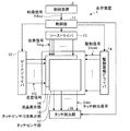
図4は、本開示の実施の形態に係る表示装置1の一構成例を表すものである。この表示装置1は、液晶表示パネルと静電容量式のタッチパネルとを一体化した、いわゆるインセルタイプの表示装置である。
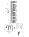
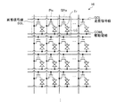
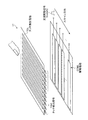
次に、タッチセンサ付き表示部15の構成例を詳細に説明する。
次に、ゲートドライバ12について説明する。ゲートドライバ12は、間欠的に線順次走査することにより、液晶表示部16の1水平ラインを順次選択するものである。
各転送回路50の入力端子Ckには、クロック信号Ck1,Ck2のうちの一方が、転送回路ごとに交互に供給される。具体的には、例えば、転送回路50(1),50(3),50(5)等の入力端子Ckにはクロック信号Ck1がそれぞれ供給され、転送回路50(2),50(4),50(6)等の入力端子Ckにはクロック信号Ck2がそれぞれ供給される。各転送回路50の入力端子Ckbには、クロック信号Ck1,Ck2のうち、入力端子Ckに入力されたものと異なる信号が供給される。具体的には、例えば、転送回路50(1),50(3),50(5)等の入力端子Ckbにはクロック信号Ck2がそれぞれ供給され、転送回路50(2),50(4),50(6)等の入力端子Ckbにはクロック信号Ck1がそれぞれ供給される。
続いて、本実施の形態の表示装置1の動作および作用について説明する。
まず、図4を参照して、表示装置1の全体動作概要を説明する。制御部11は、表示装置1の外部の制御装置2より供給された映像信号Vdispに基づいて、ゲートドライバ12、ソースドライバ13、駆動電極ドライバ14、およびタッチ検出部18に対してそれぞれ制御信号を供給し、これらがお互いに同期して動作するように制御する。ゲートドライバ12は、タッチセンサ付き表示部15の液晶表示部16に走査信号VGを供給し、表示駆動の対象となる1水平ラインを順次選択する。ソースドライバ13は、画素信号Vsigを、選択された1水平ラインを構成する各サブ画素SPixに供給する。駆動電極ドライバ14は、タッチ検出駆動の対象となる駆動電極COMLに対して交流駆動信号VcomACを順次印加すると共に、それ以外の駆動電極COMLに対して直流駆動信号VcomDCを印加する。タッチセンサ付き表示部15は、表示動作を行うと共にタッチ検出動作を行い、タッチ検出電極TDLからタッチ検出信号Vdetを出力する。タッチ検出部18は、タッチセンサ付き表示部15のタッチセンサ部17から供給されたタッチ検出信号Vdetに基づいて、外部近接物体を検出する。
次に、いくつかの図を参照して、表示装置1の動作を詳細に説明する。
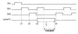
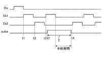
図15は、ゲートドライバ12の一動作例を表すものであり、(A)は制御信号Stvの波形を示し、(B)はクロック信号Ck1の波形を示し、(C)はクロック信号Ck2の波形を示し、(D)は走査信号VG(1)〜VG(4)の波形を示し、(E)は走査信号VG(5)〜VG(8)の波形を示し、(F)は走査信号VG(9)の波形を示す。
以上のように本実施の形態では、回路動作をとめている期間、電位保持信号を入力してリーク経路になる配線の電圧をH電位に設定することにより、充電したH電位が低下しないようにして、画質の低下を抑えることができる。
上記したように、本例の表示装置1では、シフトレジスタ52を構成する複数段の転送回路のうち、中断期間にシフト信号を保持することがある段に配置される転送回路に、電位保持信号を入力する。このため、例えば、複数段の転送回路について、所定段数(回路数)ごとに電位保持信号が入力される。上記の例では4段ごと(4回路ごと)に電位保持信号を入力しているが、4段(4回路)よりも少ない段ごとまたは4段(4回路)よりも多い段ごとに電位保持信号を入力してもよい。
図8では、中断期間にシフト信号を保持することがある転送回路(図10に示した構成の転送回路)ごとに電位保持信号線19を独立して設ける例を示した。しかしながら、シフトレジスタの構成は、これに限定されない。例えば、図16に示すように、図10に示した構成の転送回路の全てが、1つの電位保持信号線19を共用してもよい。すなわち、シフトレジスタは、中断期間において、図10に示した構成の転送回路の全てに電位保持信号pulseが入力されるように構成されてもよい。
アモルファスシリコン(a−Si)によるトランジスタは、ゲートにプラス(+)電圧を印加するとしきい値電圧Vthがプラス方向にシフトし、マイナス(−)電圧を印加するとしきい値電圧Vthがマイナス方向にシフトする。そして、しきい値電圧Vthがマイナスにシフトして、トランジスタがデプレション型になることがある。
次に、上記実施の形態および変形例で説明した表示装置の適用例について説明する。図20〜図32は、実施の形態等の表示装置が適用される電子機器の外観例を表す図である。上記実施の形態等の表示装置は、テレビジョン装置、デジタルカメラ、ノート型パーソナルコンピュータ、携帯電話等の携帯端末装置あるいはビデオカメラなどのあらゆる分野の電子機器に適用することが可能である。言い換えると、上記実施の形態等の表示装置は、外部から入力された映像信号あるいは内部で生成した映像信号を、画像あるいは映像として表示するあらゆる分野の電子機器に適用することが可能である。
図20に示す電子機器は、上記実施の形態等の表示装置が適用されるテレビジョン装置である。このテレビジョン装置は、例えば、フロントパネル511及びフィルターガラス512を含む映像表示画面部510を有しており、この映像表示画面部510は、上記実施の形態等の表示装置である。
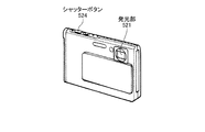
図21及び図22に示す電子機器は、上記実施の形態等の表示装置が適用されるデジタルカメラである。このデジタルカメラは、例えば、フラッシュ用の発光部521、表示部522、メニュースイッチ523及びシャッターボタン524を有しており、その表示部522は、上記実施の形態等の表示装置である。
図23に示す電子機器は、上記実施の形態等の表示装置が適用されるビデオカメラの外観を表すものである。このビデオカメラは、例えば、本体部531、この本体部531の前方側面に設けられた被写体撮影用のレンズ532、撮影時のスタート/ストップスイッチ533及び表示部534を有している。そして、表示部534は、上記の実施形態及び変形例に係る表示装置ある。
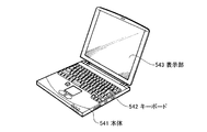
図24に示す電子機器は、上記実施の形態等の表示装置が適用されるノート型パーソナルコンピュータである。このノート型パーソナルコンピュータは、例えば、本体541、文字等の入力操作のためのキーボード542及び画像を表示する表示部543を有しており、表示部543は、上記実施の形態等の表示装置である。
図25〜図31に示す電子機器は、上記実施の形態等の表示装置が適用される携帯電話機である。この携帯電話機は、例えば、上側筐体551と下側筐体552とを連結部(ヒンジ部)553で連結したものであり、ディスプレイ554、サブディスプレイ555、ピクチャーライト556及びカメラ557を有している。そのディスプレイ554又はサブディスプレイ555は、上記の実施形態及び変形例に係る表示装置である。
図32に示す電子機器は、携帯型コンピュータ、多機能な携帯電話、音声通話可能な携帯コンピュータ又は通信可能な携帯コンピュータとして動作し、いわゆるスマートフォン、タブレット端末と呼ばれることもある、情報携帯端末である。この情報携帯端末は、例えば筐体561の表面に表示部562を有している。この表示部562は、上記実施の形態等の表示装置である。
入力されたシフト信号を一時的に保持し、中断期間を有するクロック信号に同期して、該シフト信号を次段へ順次伝達するシフト動作を行う複数段の転送回路を有し、前記シフト信号を保持する転送回路に対応する走査信号線へ前記走査信号を出力するシフトレジスタと、
前記クロック信号の前記中断期間に、前記シフト信号を保持する転送回路に該シフト信号の電位を保持するための電位保持信号を伝達する信号線と、
を含む表示装置。
前記(1)に記載の表示装置。
前記ラッチ部は、前記電位保持信号が入力されている期間において、電流リーク経路の電位を当該電位保持信号によって保つ、
前記(1)または(2)に記載の表示装置。
前記ラッチ部は、前記電位保持信号によって前記第2スイッチ部を介して前記電位が設定されている期間において、前記第3スイッチ部を通る電流リーク経路の電位を当該電位保持信号によって保つ
前記(3)に記載の表示装置。
前記(1)から(4)までのいずれか1つに記載の表示装置。
前記信号線は、前記第1転送回路毎に設けられる
前記(1)から(5)までのいずれか1つに記載の表示装置。
前記クロック信号の中断期間は、前記タッチセンサ部が前記接触または前記近接を検出するための期間として設定されている、前記(1)から(6)までのいずれか1つに記載の表示装置。
前記表示装置に入力信号を供給する制御装置と、を有する電子機器。
11 制御部
12 ゲートドライバ
13 ソースドライバ
14 駆動電極ドライバ
15 タッチセンサ付き表示部
16 液晶表示部
17 タッチセンサ部
18 タッチ検出部
19 電位保持信号線
20 画素基板
21 TFT基板
22 画素電極
23 絶縁層
30 対向基板
31 ガラス基板
32 カラーフィルタ
35 偏光板
50 転送回路
51 走査制御部
52 シフトレジスタ
Claims (8)
- 走査信号が印加される複数の走査信号線を有する表示部と、
入力されたシフト信号を一時的に保持し、中断期間を有するクロック信号に同期して、該シフト信号を次段へ順次伝達するシフト動作を行う複数段の転送回路を有し、前記シフト信号を保持する転送回路に対応する走査信号線へ前記走査信号を出力するシフトレジスタと、
前記クロック信号の前記中断期間に、前記シフト信号を保持する転送回路に該シフト信号の電位を保持するための電位保持信号を伝達する信号線と、
を含む表示装置。 - 前記複数段の転送回路は、前記中断期間に前記シフト信号を保持することがある段に配置される第1転送回路と、前記中断期間に前記シフト信号を保持することがない段に配置される第2転送回路と、を含む請求項1に記載の表示装置。
- 前記転送回路は、前段の転送回路が出力する前記シフト信号および前記電位保持信号によって前記電位が設定され、かつ、設定された前記電位が次段の転送回路が出力するシフト信号によって解除されるラッチ部と、前記ラッチ部によって保持される前記電位によってオン状態になり、前記クロック信号を前記シフト信号として出力する第1スイッチ部とを備え、
前記ラッチ部は、前記電位保持信号が入力されている期間において、電流リーク経路の電位を当該電位保持信号によって保つ請求項1または2に記載の表示装置。 - 前記転送回路は、前段の転送回路が出力する前記シフト信号によってオン状態になって前記ラッチ部に前記電位を設定するための第2スイッチ部と、後段の転送回路が出力するシフト信号によってオン状態になって前記ラッチ部に設定されている前記電位を解除する第3スイッチ部とを備え、
前記ラッチ部は、前記電位保持信号によって前記第2スイッチ部を介して前記電位が設定されている期間において、前記第3スイッチ部を通る電流リーク経路の電位を当該電位保持信号によって保つ請求項3に記載の表示装置。 - 前記電位保持信号が立ち上がるタイミングは、前記クロック信号が立ち上がるタイミングより遅く設定されている、請求項1から請求項4までのいずれか1項に記載の表示装置。
- 前記第1転送回路の数は複数であり、
前記信号線は、前記第1転送回路毎に設けられる請求項1から請求項5までのいずれか1項に記載の表示装置。 - 接触または近接を検出するタッチセンサ部をさらに備え、
前記クロック信号の中断期間は、前記タッチセンサ部が前記接触または前記近接を検出するための期間として設定されている、請求項1から請求項6までのいずれか1項に記載の表示装置。 - 請求項1から7のいずれか一項に記載の表示装置と、
前記表示装置に入力信号を供給する制御装置と、を有する電子機器。
Priority Applications (3)
| Application Number | Priority Date | Filing Date | Title |
|---|---|---|---|
| JP2013055243A JP2014182203A (ja) | 2013-03-18 | 2013-03-18 | 表示装置および電子機器 |
| US14/201,128 US9619087B2 (en) | 2013-03-18 | 2014-03-07 | Display device and electronic apparatus |
| US15/448,169 US10606384B2 (en) | 2013-03-18 | 2017-03-02 | Display device and electronic apparatus |
Applications Claiming Priority (1)
| Application Number | Priority Date | Filing Date | Title |
|---|---|---|---|
| JP2013055243A JP2014182203A (ja) | 2013-03-18 | 2013-03-18 | 表示装置および電子機器 |
Publications (1)
| Publication Number | Publication Date |
|---|---|
| JP2014182203A true JP2014182203A (ja) | 2014-09-29 |
Family
ID=51525326
Family Applications (1)
| Application Number | Title | Priority Date | Filing Date |
|---|---|---|---|
| JP2013055243A Pending JP2014182203A (ja) | 2013-03-18 | 2013-03-18 | 表示装置および電子機器 |
Country Status (2)
| Country | Link |
|---|---|
| US (2) | US9619087B2 (ja) |
| JP (1) | JP2014182203A (ja) |
Cited By (17)
| Publication number | Priority date | Publication date | Assignee | Title |
|---|---|---|---|---|
| KR20170066443A (ko) | 2014-12-05 | 2017-06-14 | 도판 인사츠 가부시키가이샤 | 표시 장치 기판, 표시 장치 기판의 제조 방법, 및 이것을 사용한 표시 장치 |
| KR20180003701A (ko) * | 2016-06-30 | 2018-01-10 | 엘지디스플레이 주식회사 | 터치센서 내장형 표시장치 |
| JP2018508854A (ja) * | 2015-01-05 | 2018-03-29 | 深▲セン▼市華星光電技術有限公司 | タッチ機能を有する表示パネル及びタッチ検知方法 |
| JP2018092161A (ja) * | 2016-11-25 | 2018-06-14 | 株式会社半導体エネルギー研究所 | 表示装置およびその動作方法 |
| KR20180079413A (ko) | 2015-12-28 | 2018-07-10 | 도판 인사츠 가부시키가이샤 | 액정 표시 장치 |
| KR20180126594A (ko) | 2016-05-13 | 2018-11-27 | 도판 인사츠 가부시키가이샤 | 표시 장치 |
| JP2018536182A (ja) * | 2015-09-28 | 2018-12-06 | 深▲せん▼市華星光電技術有限公司Shenzhen China Star Optoelectronics Technology Co., Ltd. | 表示装置、tft基板及びgoa駆動回路 |
| JP2019502148A (ja) * | 2015-11-09 | 2019-01-24 | 武漢華星光電技術有限公司 | Goa駆動回路、tft表示パネル及び表示装置 |
| WO2019017264A1 (ja) * | 2017-07-19 | 2019-01-24 | シャープ株式会社 | シフトレジスタおよびそれを備える表示装置 |
| JP2019061323A (ja) * | 2017-09-25 | 2019-04-18 | 株式会社ジャパンディスプレイ | 表示装置 |
| US10296121B2 (en) | 2015-07-09 | 2019-05-21 | Sharp Kabushiki Kaisha | Shift register, display device provided with same, and shift register driving method |
| US10629147B2 (en) | 2017-09-11 | 2020-04-21 | Sharp Kabushiki Kaisha | Display device |
| US10679578B2 (en) | 2017-09-28 | 2020-06-09 | Sharp Kabushiki Kaisha | Display device having driving circuitry with driving gate lines |
| US10777156B2 (en) | 2017-09-01 | 2020-09-15 | Sharp Kabushiki Kaisha | Display driving device and display device having electric potential controlling circuitry |
| US10902813B2 (en) | 2017-11-15 | 2021-01-26 | Sharp Kabushiki Kaisha | Shift register and display device provided with same |
| US10964244B2 (en) | 2018-09-04 | 2021-03-30 | Sharp Kabushiki Kaisha | Display device |
| US11094278B2 (en) | 2015-02-12 | 2021-08-17 | Japan Display Inc. | Display apparatus including a substrate with first and second regions including respective first and second circuit portions with different dimensions |
Families Citing this family (13)
| Publication number | Priority date | Publication date | Assignee | Title |
|---|---|---|---|---|
| US9842551B2 (en) * | 2014-06-10 | 2017-12-12 | Apple Inc. | Display driver circuitry with balanced stress |
| CN104537972B (zh) * | 2014-12-26 | 2017-05-31 | 厦门天马微电子有限公司 | 驱动电路、触控显示面板及触控显示装置 |
| CN104485080B (zh) * | 2014-12-31 | 2017-02-22 | 深圳市华星光电技术有限公司 | 用于液晶显示装置的goa电路 |
| CN104485082B (zh) * | 2014-12-31 | 2017-02-22 | 厦门天马微电子有限公司 | 一种阵列基板和触控显示装置及其驱动方法 |
| CN104505014B (zh) * | 2014-12-31 | 2017-02-22 | 厦门天马微电子有限公司 | 一种驱动电路、阵列基板和触控显示装置及其驱动方法 |
| CN104808862B (zh) * | 2015-05-14 | 2018-02-23 | 厦门天马微电子有限公司 | 阵列基板、触控显示面板和阵列基板的驱动方法 |
| US10365751B2 (en) * | 2015-07-10 | 2019-07-30 | Tpk Touch Solutions (Xiamen) Inc. | Display device with three-dimension input module |
| CN110111754B (zh) * | 2015-07-17 | 2021-08-10 | 群创光电股份有限公司 | 栅极驱动电路 |
| CN105183224B (zh) * | 2015-09-07 | 2018-08-07 | 厦门天马微电子有限公司 | 驱动电路、触控显示面板及触控显示装置 |
| TWI638298B (zh) * | 2015-12-31 | 2018-10-11 | 禾瑞亞科技股份有限公司 | 觸控方法、觸控處理系統與電子裝置 |
| US10579197B2 (en) | 2015-12-31 | 2020-03-03 | Egalax_Empia Technology Inc. | Touch sensitive processing method |
| JP2019090927A (ja) * | 2017-11-15 | 2019-06-13 | シャープ株式会社 | 走査信号線駆動回路およびそれを備えた表示装置 |
| CN117289818A (zh) * | 2023-08-25 | 2023-12-26 | 湖北长江新型显示产业创新中心有限公司 | 扫描信号驱动电路、显示面板、显示装置及驱动方法 |
Citations (3)
| Publication number | Priority date | Publication date | Assignee | Title |
|---|---|---|---|---|
| JP2000338919A (ja) * | 1999-03-25 | 2000-12-08 | Seiko Epson Corp | 電気光学装置の駆動回路および電気光学装置および投射型表示装置 |
| JP2007317288A (ja) * | 2006-05-25 | 2007-12-06 | Mitsubishi Electric Corp | シフトレジスタ回路およびそれを備える画像表示装置 |
| WO2012137800A1 (ja) * | 2011-04-08 | 2012-10-11 | シャープ株式会社 | 表示装置およびその駆動方法、並びに電子機器 |
Family Cites Families (5)
| Publication number | Priority date | Publication date | Assignee | Title |
|---|---|---|---|---|
| KR20100083370A (ko) * | 2009-01-13 | 2010-07-22 | 삼성전자주식회사 | 게이트 구동회로 및 이를 갖는 표시장치 |
| JP2010250030A (ja) | 2009-04-15 | 2010-11-04 | Sharp Corp | シフトレジスタおよびそれを備えた表示装置、ならびにシフトレジスタの駆動方法 |
| BR112012000960A2 (pt) * | 2009-07-15 | 2016-03-15 | Sharp Kk | circuito acionador da linha do sinal de digitalização e dispositivo de exibição tendo o mesmo |
| JP5191522B2 (ja) | 2010-10-29 | 2013-05-08 | 三菱電機株式会社 | シフトレジスタ回路 |
| CN102750062B (zh) * | 2012-06-29 | 2016-02-10 | 京东方科技集团股份有限公司 | 一种电容式内嵌触摸屏及显示装置 |
-
2013
- 2013-03-18 JP JP2013055243A patent/JP2014182203A/ja active Pending
-
2014
- 2014-03-07 US US14/201,128 patent/US9619087B2/en active Active
-
2017
- 2017-03-02 US US15/448,169 patent/US10606384B2/en active Active
Patent Citations (3)
| Publication number | Priority date | Publication date | Assignee | Title |
|---|---|---|---|---|
| JP2000338919A (ja) * | 1999-03-25 | 2000-12-08 | Seiko Epson Corp | 電気光学装置の駆動回路および電気光学装置および投射型表示装置 |
| JP2007317288A (ja) * | 2006-05-25 | 2007-12-06 | Mitsubishi Electric Corp | シフトレジスタ回路およびそれを備える画像表示装置 |
| WO2012137800A1 (ja) * | 2011-04-08 | 2012-10-11 | シャープ株式会社 | 表示装置およびその駆動方法、並びに電子機器 |
Cited By (27)
| Publication number | Priority date | Publication date | Assignee | Title |
|---|---|---|---|---|
| KR20170066443A (ko) | 2014-12-05 | 2017-06-14 | 도판 인사츠 가부시키가이샤 | 표시 장치 기판, 표시 장치 기판의 제조 방법, 및 이것을 사용한 표시 장치 |
| JP2018508854A (ja) * | 2015-01-05 | 2018-03-29 | 深▲セン▼市華星光電技術有限公司 | タッチ機能を有する表示パネル及びタッチ検知方法 |
| US12008973B2 (en) | 2015-02-12 | 2024-06-11 | Japan Display Inc. | Display apparatus including a substrate with first and second regions including respective first and second circuit portions with different dimensions |
| US11094278B2 (en) | 2015-02-12 | 2021-08-17 | Japan Display Inc. | Display apparatus including a substrate with first and second regions including respective first and second circuit portions with different dimensions |
| US10296121B2 (en) | 2015-07-09 | 2019-05-21 | Sharp Kabushiki Kaisha | Shift register, display device provided with same, and shift register driving method |
| JP2018536182A (ja) * | 2015-09-28 | 2018-12-06 | 深▲せん▼市華星光電技術有限公司Shenzhen China Star Optoelectronics Technology Co., Ltd. | 表示装置、tft基板及びgoa駆動回路 |
| KR102057822B1 (ko) | 2015-09-28 | 2019-12-19 | 센젠 차이나 스타 옵토일렉트로닉스 테크놀로지 컴퍼니 리미티드 | 디스플레이 장치, tft 기판 및 goa 구동 회로 |
| JP2019502148A (ja) * | 2015-11-09 | 2019-01-24 | 武漢華星光電技術有限公司 | Goa駆動回路、tft表示パネル及び表示装置 |
| US10817105B2 (en) | 2015-12-28 | 2020-10-27 | Toppan Printing Co., Ltd. | Liquid crystal display device |
| KR20180079413A (ko) | 2015-12-28 | 2018-07-10 | 도판 인사츠 가부시키가이샤 | 액정 표시 장치 |
| KR20180126594A (ko) | 2016-05-13 | 2018-11-27 | 도판 인사츠 가부시키가이샤 | 표시 장치 |
| KR20180003701A (ko) * | 2016-06-30 | 2018-01-10 | 엘지디스플레이 주식회사 | 터치센서 내장형 표시장치 |
| KR102545790B1 (ko) * | 2016-06-30 | 2023-06-21 | 엘지디스플레이 주식회사 | 터치센서 내장형 표시장치 |
| US11361726B2 (en) | 2016-11-25 | 2022-06-14 | Semiconductor Energy Laboratory Co., Ltd. | Display device and operating method thereof |
| US11715438B2 (en) | 2016-11-25 | 2023-08-01 | Semiconductor Energy Laboratory Co., Ltd. | Display device and operating method thereof |
| US12008975B2 (en) | 2016-11-25 | 2024-06-11 | Semiconductor Energy Laboratory Co., Ltd. | Display device and operating method thereof |
| JP7430213B2 (ja) | 2016-11-25 | 2024-02-09 | 株式会社半導体エネルギー研究所 | 表示装置 |
| JP2022082810A (ja) * | 2016-11-25 | 2022-06-02 | 株式会社半導体エネルギー研究所 | 表示装置 |
| JP2018092161A (ja) * | 2016-11-25 | 2018-06-14 | 株式会社半導体エネルギー研究所 | 表示装置およびその動作方法 |
| JP7058111B2 (ja) | 2016-11-25 | 2022-04-21 | 株式会社半導体エネルギー研究所 | 表示装置 |
| WO2019017264A1 (ja) * | 2017-07-19 | 2019-01-24 | シャープ株式会社 | シフトレジスタおよびそれを備える表示装置 |
| US10777156B2 (en) | 2017-09-01 | 2020-09-15 | Sharp Kabushiki Kaisha | Display driving device and display device having electric potential controlling circuitry |
| US10629147B2 (en) | 2017-09-11 | 2020-04-21 | Sharp Kabushiki Kaisha | Display device |
| JP2019061323A (ja) * | 2017-09-25 | 2019-04-18 | 株式会社ジャパンディスプレイ | 表示装置 |
| US10679578B2 (en) | 2017-09-28 | 2020-06-09 | Sharp Kabushiki Kaisha | Display device having driving circuitry with driving gate lines |
| US10902813B2 (en) | 2017-11-15 | 2021-01-26 | Sharp Kabushiki Kaisha | Shift register and display device provided with same |
| US10964244B2 (en) | 2018-09-04 | 2021-03-30 | Sharp Kabushiki Kaisha | Display device |
Also Published As
| Publication number | Publication date |
|---|---|
| US9619087B2 (en) | 2017-04-11 |
| US20140267156A1 (en) | 2014-09-18 |
| US10606384B2 (en) | 2020-03-31 |
| US20170177131A1 (en) | 2017-06-22 |
Similar Documents
| Publication | Publication Date | Title |
|---|---|---|
| US10606384B2 (en) | Display device and electronic apparatus | |
| JP5758825B2 (ja) | 表示装置、表示方法、および電子機器 | |
| US10795497B2 (en) | Detection device driven with two different modes | |
| JP5818722B2 (ja) | 液晶表示装置、表示駆動方法、電子機器 | |
| JP6046592B2 (ja) | 表示装置及び電子機器 | |
| TWI608388B (zh) | 顯示裝置及其驅動方法與驅動電路 | |
| JP5455126B2 (ja) | タッチ検出機能付き表示装置、駆動方法、および電子機器 | |
| JP5726606B2 (ja) | タッチ検出機能付き表示パネルおよびその駆動方法、駆動回路、ならびに電子機器 | |
| TWI467424B (zh) | 觸摸偵測功能顯示裝置,驅動電路,觸摸偵測功能顯示裝置之驅動方法及電子設備 | |
| US10373577B2 (en) | Display device and electronic apparatus | |
| CN109062428B (zh) | 驱动器集成电路及包括该驱动器集成电路的显示设备 | |
| US10339884B2 (en) | Display device, method of driving display device, and electronic apparatus | |
| KR20180025507A (ko) | 터치형 표시장치 | |
| JP2018106057A (ja) | 表示装置及び単位レジスタ回路 | |
| US9146635B2 (en) | Touch panel equipped display device and control method for same | |
| WO2019033792A1 (zh) | 阵列基板及其驱动方法和显示装置 | |
| JP2015122125A (ja) | タッチ検出機能付き表示パネルおよびその駆動方法、駆動回路、ならびに電子機器 | |
| JP2015087608A (ja) | タッチパネル付き液晶表示装置 | |
| JP5687757B2 (ja) | タッチ検出機能付き表示装置、駆動方法、および電子機器 | |
| JP2009086170A (ja) | 電気光学装置及び電気光学装置の駆動方法並びに電子機器 | |
| CN106328040B (zh) | Gip电路及其驱动方法和平板显示装置 | |
| JP2009086171A (ja) | 電気光学装置及び電気光学装置の駆動方法並びに電子機器 | |
| CN104008716B (zh) | 显示装置及电子设备 | |
| JP2009086172A (ja) | 電気光学装置及び電気光学装置の駆動方法並びに電子機器 |
Legal Events
| Date | Code | Title | Description |
|---|---|---|---|
| A621 | Written request for application examination |
Free format text: JAPANESE INTERMEDIATE CODE: A621 Effective date: 20150312 |
|
| A977 | Report on retrieval |
Free format text: JAPANESE INTERMEDIATE CODE: A971007 Effective date: 20150619 |
|
| A131 | Notification of reasons for refusal |
Free format text: JAPANESE INTERMEDIATE CODE: A131 Effective date: 20150728 |
|
| A521 | Written amendment |
Free format text: JAPANESE INTERMEDIATE CODE: A523 Effective date: 20150924 |
|
| A02 | Decision of refusal |
Free format text: JAPANESE INTERMEDIATE CODE: A02 Effective date: 20160308 |