JP2014183172A - 半導体素子搭載用基板の製造方法 - Google Patents
半導体素子搭載用基板の製造方法 Download PDFInfo
- Publication number
- JP2014183172A JP2014183172A JP2013056466A JP2013056466A JP2014183172A JP 2014183172 A JP2014183172 A JP 2014183172A JP 2013056466 A JP2013056466 A JP 2013056466A JP 2013056466 A JP2013056466 A JP 2013056466A JP 2014183172 A JP2014183172 A JP 2014183172A
- Authority
- JP
- Japan
- Prior art keywords
- resist
- exposure
- layer
- substrate
- mask
- Prior art date
- Legal status (The legal status is an assumption and is not a legal conclusion. Google has not performed a legal analysis and makes no representation as to the accuracy of the status listed.)
- Granted
Links
Images


Classifications
-
- H—ELECTRICITY
- H10—SEMICONDUCTOR DEVICES; ELECTRIC SOLID-STATE DEVICES NOT OTHERWISE PROVIDED FOR
- H10W—GENERIC PACKAGES, INTERCONNECTIONS, CONNECTORS OR OTHER CONSTRUCTIONAL DETAILS OF DEVICES COVERED BY CLASS H10
- H10W70/00—Package substrates; Interposers; Redistribution layers [RDL]
- H10W70/01—Manufacture or treatment
- H10W70/04—Manufacture or treatment of leadframes
- H10W70/042—Etching
-
- G—PHYSICS
- G03—PHOTOGRAPHY; CINEMATOGRAPHY; ANALOGOUS TECHNIQUES USING WAVES OTHER THAN OPTICAL WAVES; ELECTROGRAPHY; HOLOGRAPHY
- G03F—PHOTOMECHANICAL PRODUCTION OF TEXTURED OR PATTERNED SURFACES, e.g. FOR PRINTING, FOR PROCESSING OF SEMICONDUCTOR DEVICES; MATERIALS THEREFOR; ORIGINALS THEREFOR; APPARATUS SPECIALLY ADAPTED THEREFOR
- G03F7/00—Photomechanical, e.g. photolithographic, production of textured or patterned surfaces, e.g. printing surfaces; Materials therefor, e.g. comprising photoresists; Apparatus specially adapted therefor
- G03F7/20—Exposure; Apparatus therefor
- G03F7/2022—Multi-step exposure, e.g. hybrid; backside exposure; blanket exposure, e.g. for image reversal; edge exposure, e.g. for edge bead removal; corrective exposure
-
- G—PHYSICS
- G03—PHOTOGRAPHY; CINEMATOGRAPHY; ANALOGOUS TECHNIQUES USING WAVES OTHER THAN OPTICAL WAVES; ELECTROGRAPHY; HOLOGRAPHY
- G03F—PHOTOMECHANICAL PRODUCTION OF TEXTURED OR PATTERNED SURFACES, e.g. FOR PRINTING, FOR PROCESSING OF SEMICONDUCTOR DEVICES; MATERIALS THEREFOR; ORIGINALS THEREFOR; APPARATUS SPECIALLY ADAPTED THEREFOR
- G03F7/00—Photomechanical, e.g. photolithographic, production of textured or patterned surfaces, e.g. printing surfaces; Materials therefor, e.g. comprising photoresists; Apparatus specially adapted therefor
- G03F7/26—Processing photosensitive materials; Apparatus therefor
- G03F7/30—Imagewise removal using liquid means
- G03F7/32—Liquid compositions therefor, e.g. developers
-
- H—ELECTRICITY
- H10—SEMICONDUCTOR DEVICES; ELECTRIC SOLID-STATE DEVICES NOT OTHERWISE PROVIDED FOR
- H10W—GENERIC PACKAGES, INTERCONNECTIONS, CONNECTORS OR OTHER CONSTRUCTIONAL DETAILS OF DEVICES COVERED BY CLASS H10
- H10W70/00—Package substrates; Interposers; Redistribution layers [RDL]
- H10W70/01—Manufacture or treatment
- H10W70/04—Manufacture or treatment of leadframes
-
- H—ELECTRICITY
- H10—SEMICONDUCTOR DEVICES; ELECTRIC SOLID-STATE DEVICES NOT OTHERWISE PROVIDED FOR
- H10W—GENERIC PACKAGES, INTERCONNECTIONS, CONNECTORS OR OTHER CONSTRUCTIONAL DETAILS OF DEVICES COVERED BY CLASS H10
- H10W70/00—Package substrates; Interposers; Redistribution layers [RDL]
- H10W70/01—Manufacture or treatment
- H10W70/04—Manufacture or treatment of leadframes
- H10W70/041—Connecting or disconnecting interconnections to or from leadframes, e.g. connecting bond wires or bumps
-
- H—ELECTRICITY
- H10—SEMICONDUCTOR DEVICES; ELECTRIC SOLID-STATE DEVICES NOT OTHERWISE PROVIDED FOR
- H10W—GENERIC PACKAGES, INTERCONNECTIONS, CONNECTORS OR OTHER CONSTRUCTIONAL DETAILS OF DEVICES COVERED BY CLASS H10
- H10W70/00—Package substrates; Interposers; Redistribution layers [RDL]
- H10W70/01—Manufacture or treatment
- H10W70/05—Manufacture or treatment of insulating or insulated package substrates, or of interposers, or of redistribution layers
-
- H—ELECTRICITY
- H10—SEMICONDUCTOR DEVICES; ELECTRIC SOLID-STATE DEVICES NOT OTHERWISE PROVIDED FOR
- H10W—GENERIC PACKAGES, INTERCONNECTIONS, CONNECTORS OR OTHER CONSTRUCTIONAL DETAILS OF DEVICES COVERED BY CLASS H10
- H10W70/00—Package substrates; Interposers; Redistribution layers [RDL]
- H10W70/40—Leadframes
- H10W70/421—Shapes or dispositions
- H10W70/424—Cross-sectional shapes
-
- H—ELECTRICITY
- H10—SEMICONDUCTOR DEVICES; ELECTRIC SOLID-STATE DEVICES NOT OTHERWISE PROVIDED FOR
- H10W—GENERIC PACKAGES, INTERCONNECTIONS, CONNECTORS OR OTHER CONSTRUCTIONAL DETAILS OF DEVICES COVERED BY CLASS H10
- H10W70/00—Package substrates; Interposers; Redistribution layers [RDL]
- H10W70/60—Insulating or insulated package substrates; Interposers; Redistribution layers
- H10W70/67—Insulating or insulated package substrates; Interposers; Redistribution layers characterised by their insulating layers or insulating parts
- H10W70/69—Insulating materials thereof
-
- H—ELECTRICITY
- H10—SEMICONDUCTOR DEVICES; ELECTRIC SOLID-STATE DEVICES NOT OTHERWISE PROVIDED FOR
- H10W—GENERIC PACKAGES, INTERCONNECTIONS, CONNECTORS OR OTHER CONSTRUCTIONAL DETAILS OF DEVICES COVERED BY CLASS H10
- H10W74/00—Encapsulations, e.g. protective coatings
- H10W74/01—Manufacture or treatment
- H10W74/016—Manufacture or treatment using moulds
-
- H—ELECTRICITY
- H10—SEMICONDUCTOR DEVICES; ELECTRIC SOLID-STATE DEVICES NOT OTHERWISE PROVIDED FOR
- H10W—GENERIC PACKAGES, INTERCONNECTIONS, CONNECTORS OR OTHER CONSTRUCTIONAL DETAILS OF DEVICES COVERED BY CLASS H10
- H10W70/00—Package substrates; Interposers; Redistribution layers [RDL]
- H10W70/60—Insulating or insulated package substrates; Interposers; Redistribution layers
- H10W70/62—Insulating or insulated package substrates; Interposers; Redistribution layers characterised by their interconnections
- H10W70/66—Conductive materials thereof
Landscapes
- Physics & Mathematics (AREA)
- General Physics & Mathematics (AREA)
- Photosensitive Polymer And Photoresist Processing (AREA)
- Exposure And Positioning Against Photoresist Photosensitive Materials (AREA)
- Engineering & Computer Science (AREA)
- Ceramic Engineering (AREA)
- Manufacturing Of Printed Wiring (AREA)
- Geometry (AREA)
Abstract
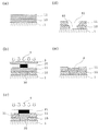
【解決手段】メインの感光波長が異なる2種類のドライフィルムレジストを用いて基板1表面に複数層のレジスト層10,11を形成する工程と、複数層のレジスト層の上から第1の露光用マスク20を用いて複数層のレジスト層の中から特定のレジスト層10のみを第1のパターンに感光する第1の露光工程と、複数層のレジスト層の上から第2の露光用マスク21を用いて複数層のレジスト層の中から別のレジスト層11を第2のパターンに感光する第2の露光工程と、複数層のレジスト層の未露光部分30,31を除去して基板の表面を部分的に露出させて開口部40,41を有するレジストマスク10,11を形成する現像工程と、基板の表面が露出している部分に所望のめっきを施してめっき層2を形成する工程と、レジストマスクを除去する工程を順次経ること。
【選択図】 図2
Description
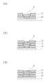
次に、本発明の半導体素子搭載用基板の製造方法の一実施例を図2に基づいて説明する。図2(a)に示すように、導電性を有する基板1として厚さ0.15mmのSUS430を用いて、基板1の両面に厚さ25μmのドライフィルムレジスト(旭化成イーマテリアルズ製:ADH−252)をラミネートしレジスト層10を形成した(裏面側は図示せず)。この時のラミネート条件は、ロール温度105℃、ロール圧力0.5MPa、送り速度2.5m/minで行なった。尚、ラミネートしたドライフィルムレジストはネガ型レジストであって、h線照射(感光波長:405nm)による露光が可能なドライフィルムレジストである。
次に、3層のドライフィルムレジストを使用した場合の実施例を図3に基づいて説明する。図3(a)に示すように、基板1として厚さ0.15mmのCu板を用いて、基板1の両面に厚さ25μmのドライフィルムレジスト(旭化成イーマテリアルズ製:ADH−252)をラミネートしレジスト層10を形成した(裏面側は図示せず)。この時のラミネート条件は、ロール温度105℃、ロール圧力0.5MPa、送り速度2.5m/minで行なった。尚、ラミネートしたドライフィルムレジストはネガ型レジストであって、h線照射(感光波長:405nm)による露光が可能なレジストである。
同じく、3層のドライフィルムレジストを使用した場合の実施例を図4に基づいて説明する。図4(a)に示すように、基板1として厚さ0.15mmのCu板を用いて、基板1の両面に厚さ25μmのドライフィルムレジスト(旭化成イーマテリアルズ製:AQ−2558)をラミネートしレジスト層10を形成した(裏面側は図示せず)。この時のラミネート条件は、ロール温度105℃、ロール圧力0.5MPa、送り速度2.5m/minで行なった。尚、ラミネートしたドライフィルムレジストはネガ型レジストであって、i線照射(感光波長:365nm)による露光が可能なレジストである。
2・・・めっき層(金属層、電極層)
3・・・バンドパスフィルタ
4・・・光源
10,11,12・・・レジスト層(レジストマスク)
20,21・・・マスク
30,31,32・・・未露光部分
40,41,42・・・開口部
Claims (4)
- 導電性を有する基板の表面に端子等となるめっき層を備えた半導体素子搭載用基板の製造方法であって、メインの感光波長が異なる2種類のドライフィルムレジストを用いて前記基板の表面にこの2種類のドライフィルムレジストで複数層のレジスト層を形成する工程と、前記複数層のレジスト層の上から第1の露光用マスクを用いて前記複数層のレジスト層の中から特定のレジスト層のみを第1のパターンに感光する第1の露光工程と、前記複数層のレジスト層の上から第2の露光用マスクを用いて前記複数層のレジスト層の中から別のレジスト層を第2のパターンに感光する第2の露光工程と、前記複数層のレジスト層の未露光部分を除去して前記基板の表面を部分的に露出させて開口部を有するレジストマスクを形成する現像工程と、前記基板の表面が露出している部分に所望のめっきを施してめっき層を形成する工程と、前記レジストマスクを除去する工程を順次経ることを特徴とする半導体素子搭載用基板の製造方法。
- 前記第1の露光用マスクと前記第2の露光用マスクは描かれているパターンが異なり、この描かれているパターンが異なる第1と第2の露光用マスクを用いて前記2種類のドライフィルムレジストからなる前記複数層のレジスト層を露光し現像することによって、前記基板表面が露出しているめっき用のレジストマスクの前記開口部の断面に段差が形成されることを特徴とする請求項1に記載の半導体素子搭載用基板の製造方法。
- 露光の際に、バンドパスフィルタを用いて所定の波長の紫外線を選択して前記第1の露光工程または前記第2の露光工程を行うことを特徴とする請求項1または請求項2に記載の半導体素子搭載用基板の製造方法。
- 露光の際に、選ばれたレジスト層のみを露光できる波長の紫外線を使用して前記第1の露光工程または前記第2の露光工程を行うことを特徴とする請求項1または請求項2に記載の半導体素子搭載用基板の製造方法。
Priority Applications (6)
| Application Number | Priority Date | Filing Date | Title |
|---|---|---|---|
| JP2013056466A JP5979495B2 (ja) | 2013-03-19 | 2013-03-19 | 半導体素子搭載用基板の製造方法 |
| CN201480013843.3A CN105190870B (zh) | 2013-03-19 | 2014-03-11 | 半导体元件搭载用基板的制造方法 |
| KR1020157019303A KR102162913B1 (ko) | 2013-03-19 | 2014-03-11 | 반도체 소자 탑재용 기판의 제조방법 |
| US14/777,834 US10204801B2 (en) | 2013-03-19 | 2014-03-11 | Method for producing substrate for semiconductor element mounting |
| PCT/JP2014/056304 WO2014148308A1 (ja) | 2013-03-19 | 2014-03-11 | 半導体素子搭載用基板の製造方法 |
| TW103109919A TWI588947B (zh) | 2013-03-19 | 2014-03-17 | A method of manufacturing a semiconductor element mounting substrate |
Applications Claiming Priority (1)
| Application Number | Priority Date | Filing Date | Title |
|---|---|---|---|
| JP2013056466A JP5979495B2 (ja) | 2013-03-19 | 2013-03-19 | 半導体素子搭載用基板の製造方法 |
Publications (2)
| Publication Number | Publication Date |
|---|---|
| JP2014183172A true JP2014183172A (ja) | 2014-09-29 |
| JP5979495B2 JP5979495B2 (ja) | 2016-08-24 |
Family
ID=51579995
Family Applications (1)
| Application Number | Title | Priority Date | Filing Date |
|---|---|---|---|
| JP2013056466A Expired - Fee Related JP5979495B2 (ja) | 2013-03-19 | 2013-03-19 | 半導体素子搭載用基板の製造方法 |
Country Status (6)
| Country | Link |
|---|---|
| US (1) | US10204801B2 (ja) |
| JP (1) | JP5979495B2 (ja) |
| KR (1) | KR102162913B1 (ja) |
| CN (1) | CN105190870B (ja) |
| TW (1) | TWI588947B (ja) |
| WO (1) | WO2014148308A1 (ja) |
Cited By (4)
| Publication number | Priority date | Publication date | Assignee | Title |
|---|---|---|---|---|
| JP2016127261A (ja) * | 2014-12-27 | 2016-07-11 | 日立マクセル株式会社 | 半導体装置用基板、半導体装置用基板の製造方法、及び半導体装置 |
| JP2019009238A (ja) * | 2017-06-22 | 2019-01-17 | 大口マテリアル株式会社 | 半導体素子搭載用基板及び半導体装置、並びに半導体素子搭載用基板の製造方法 |
| JP2019012788A (ja) * | 2017-06-30 | 2019-01-24 | 大口マテリアル株式会社 | 半導体素子搭載用基板及びその製造方法 |
| JP2020013838A (ja) * | 2018-07-13 | 2020-01-23 | 大口マテリアル株式会社 | 半導体素子搭載用基板の製造方法 |
Families Citing this family (7)
| Publication number | Priority date | Publication date | Assignee | Title |
|---|---|---|---|---|
| JP5979495B2 (ja) | 2013-03-19 | 2016-08-24 | Shマテリアル株式会社 | 半導体素子搭載用基板の製造方法 |
| CN105404418B (zh) * | 2015-11-03 | 2018-09-04 | 京东方科技集团股份有限公司 | 触控屏及其制备方法、显示面板和显示装置 |
| EP3805423B1 (en) * | 2017-09-18 | 2026-03-11 | Google LLC | Reducing junction resistance variation in two-step deposition processes |
| US11764062B2 (en) * | 2017-11-13 | 2023-09-19 | Taiwan Semiconductor Manufacturing Company, Ltd. | Method of forming semiconductor structure |
| CN113140448B (zh) * | 2020-01-16 | 2022-10-28 | 芯恩(青岛)集成电路有限公司 | 一种半导体结构及其制作方法 |
| CN116235284A (zh) * | 2020-08-26 | 2023-06-06 | 奔马有限公司 | 球搭载用掩模及其制造方法 |
| CN119689790A (zh) * | 2024-11-29 | 2025-03-25 | 合肥九思电子科技有限公司 | 一种干膜光刻倒梯形结构及其制备方法 |
Citations (4)
| Publication number | Priority date | Publication date | Assignee | Title |
|---|---|---|---|---|
| JPH065631A (ja) * | 1992-06-23 | 1994-01-14 | Nec Corp | 金属電極の形成方法 |
| JP2000022131A (ja) * | 1998-06-30 | 2000-01-21 | Fujitsu Quantum Devices Kk | 半導体装置およびその製造方法 |
| JP2004119728A (ja) * | 2002-09-26 | 2004-04-15 | Sanyo Electric Co Ltd | 回路装置の製造方法 |
| US20130026639A1 (en) * | 2010-02-19 | 2013-01-31 | International Business Machines Corporation | Method of fabricating dual damascene structures using a multilevel multiple exposure patterning scheme |
Family Cites Families (8)
| Publication number | Priority date | Publication date | Assignee | Title |
|---|---|---|---|---|
| CN1110065C (zh) * | 2000-04-05 | 2003-05-28 | 信息产业部电子第十三研究所 | 半导体器件栅帽与栅足自对准的t形栅加工方法 |
| JP3626075B2 (ja) * | 2000-06-20 | 2005-03-02 | 九州日立マクセル株式会社 | 半導体装置の製造方法 |
| JP4508064B2 (ja) | 2005-09-30 | 2010-07-21 | 住友金属鉱山株式会社 | 半導体装置用配線基板の製造方法 |
| US7579137B2 (en) * | 2005-12-24 | 2009-08-25 | International Business Machines Corporation | Method for fabricating dual damascene structures |
| US7476980B2 (en) * | 2006-06-27 | 2009-01-13 | Infineon Technologies Ag | Die configurations and methods of manufacture |
| JP5626785B2 (ja) * | 2010-09-27 | 2014-11-19 | Shマテリアル株式会社 | 半導体素子搭載用リードフレームおよびその製造方法 |
| US8455312B2 (en) * | 2011-09-12 | 2013-06-04 | Cindy X. Qiu | Fabrication methods for T-gate and inverted L-gate structure for high frequency devices and circuits |
| JP5979495B2 (ja) | 2013-03-19 | 2016-08-24 | Shマテリアル株式会社 | 半導体素子搭載用基板の製造方法 |
-
2013
- 2013-03-19 JP JP2013056466A patent/JP5979495B2/ja not_active Expired - Fee Related
-
2014
- 2014-03-11 WO PCT/JP2014/056304 patent/WO2014148308A1/ja not_active Ceased
- 2014-03-11 CN CN201480013843.3A patent/CN105190870B/zh not_active Expired - Fee Related
- 2014-03-11 US US14/777,834 patent/US10204801B2/en active Active
- 2014-03-11 KR KR1020157019303A patent/KR102162913B1/ko not_active Expired - Fee Related
- 2014-03-17 TW TW103109919A patent/TWI588947B/zh not_active IP Right Cessation
Patent Citations (4)
| Publication number | Priority date | Publication date | Assignee | Title |
|---|---|---|---|---|
| JPH065631A (ja) * | 1992-06-23 | 1994-01-14 | Nec Corp | 金属電極の形成方法 |
| JP2000022131A (ja) * | 1998-06-30 | 2000-01-21 | Fujitsu Quantum Devices Kk | 半導体装置およびその製造方法 |
| JP2004119728A (ja) * | 2002-09-26 | 2004-04-15 | Sanyo Electric Co Ltd | 回路装置の製造方法 |
| US20130026639A1 (en) * | 2010-02-19 | 2013-01-31 | International Business Machines Corporation | Method of fabricating dual damascene structures using a multilevel multiple exposure patterning scheme |
Cited By (7)
| Publication number | Priority date | Publication date | Assignee | Title |
|---|---|---|---|---|
| JP2016127261A (ja) * | 2014-12-27 | 2016-07-11 | 日立マクセル株式会社 | 半導体装置用基板、半導体装置用基板の製造方法、及び半導体装置 |
| JP2019169729A (ja) * | 2014-12-27 | 2019-10-03 | マクセルホールディングス株式会社 | 半導体装置用基板および半導体装置 |
| JP2021005739A (ja) * | 2014-12-27 | 2021-01-14 | マクセルホールディングス株式会社 | 半導体装置用基板及びその製造方法、半導体装置 |
| JP2019009238A (ja) * | 2017-06-22 | 2019-01-17 | 大口マテリアル株式会社 | 半導体素子搭載用基板及び半導体装置、並びに半導体素子搭載用基板の製造方法 |
| JP2019012788A (ja) * | 2017-06-30 | 2019-01-24 | 大口マテリアル株式会社 | 半導体素子搭載用基板及びその製造方法 |
| JP2020013838A (ja) * | 2018-07-13 | 2020-01-23 | 大口マテリアル株式会社 | 半導体素子搭載用基板の製造方法 |
| JP7059139B2 (ja) | 2018-07-13 | 2022-04-25 | 大口マテリアル株式会社 | 半導体素子搭載用基板の製造方法 |
Also Published As
| Publication number | Publication date |
|---|---|
| TW201508869A (zh) | 2015-03-01 |
| CN105190870B (zh) | 2018-02-27 |
| JP5979495B2 (ja) | 2016-08-24 |
| TWI588947B (zh) | 2017-06-21 |
| WO2014148308A1 (ja) | 2014-09-25 |
| CN105190870A (zh) | 2015-12-23 |
| US10204801B2 (en) | 2019-02-12 |
| KR20150135203A (ko) | 2015-12-02 |
| KR102162913B1 (ko) | 2020-10-07 |
| US20160300732A1 (en) | 2016-10-13 |
Similar Documents
| Publication | Publication Date | Title |
|---|---|---|
| JP5979495B2 (ja) | 半導体素子搭載用基板の製造方法 | |
| JP5370330B2 (ja) | 半導体素子搭載用基板の製造方法 | |
| TWI429361B (zh) | 配線電路基板的製造方法 | |
| JP5175779B2 (ja) | 配線回路基板の製造方法 | |
| TWI605553B (zh) | Semiconductor device mounting substrate and method for manufacturing the same | |
| TW201742218A (zh) | 半導體元件搭載用基板、半導體裝置及光半導體裝置、以及該等之製造方法 | |
| JP6366034B2 (ja) | 半導体装置用リードフレーム及びその製造方法 | |
| TWI637424B (zh) | Semiconductor element mounting substrate and method of manufacturing the same | |
| JP7426560B2 (ja) | メッキ用パターン版及び配線基板の製造方法 | |
| CN101772274A (zh) | 线路基板的表面电镀方法 | |
| JP6489615B2 (ja) | 半導体素子搭載用基板、半導体装置及びそれらの製造方法 | |
| JP2018018864A (ja) | 半導体素子搭載用基板及び半導体装置、並びにそれらの製造方法 | |
| JP2017034095A (ja) | 半導体素子搭載用基板、半導体装置及びそれらの製造方法 | |
| JP6432943B2 (ja) | リードフレームの製造方法 | |
| CN115776772A (zh) | 台阶线路印制电路板制作方法 |
Legal Events
| Date | Code | Title | Description |
|---|---|---|---|
| A621 | Written request for application examination |
Free format text: JAPANESE INTERMEDIATE CODE: A621 Effective date: 20150804 |
|
| TRDD | Decision of grant or rejection written | ||
| A01 | Written decision to grant a patent or to grant a registration (utility model) |
Free format text: JAPANESE INTERMEDIATE CODE: A01 Effective date: 20160628 |
|
| A61 | First payment of annual fees (during grant procedure) |
Free format text: JAPANESE INTERMEDIATE CODE: A61 Effective date: 20160714 |
|
| R150 | Certificate of patent or registration of utility model |
Ref document number: 5979495 Country of ref document: JP Free format text: JAPANESE INTERMEDIATE CODE: R150 |
|
| S111 | Request for change of ownership or part of ownership |
Free format text: JAPANESE INTERMEDIATE CODE: R313113 |
|
| R350 | Written notification of registration of transfer |
Free format text: JAPANESE INTERMEDIATE CODE: R350 |
|
| R250 | Receipt of annual fees |
Free format text: JAPANESE INTERMEDIATE CODE: R250 |
|
| R250 | Receipt of annual fees |
Free format text: JAPANESE INTERMEDIATE CODE: R250 |
|
| R250 | Receipt of annual fees |
Free format text: JAPANESE INTERMEDIATE CODE: R250 |
|
| R250 | Receipt of annual fees |
Free format text: JAPANESE INTERMEDIATE CODE: R250 |
|
| R250 | Receipt of annual fees |
Free format text: JAPANESE INTERMEDIATE CODE: R250 |
|
| S111 | Request for change of ownership or part of ownership |
Free format text: JAPANESE INTERMEDIATE CODE: R313113 |
|
| R350 | Written notification of registration of transfer |
Free format text: JAPANESE INTERMEDIATE CODE: R350 |
|
| LAPS | Cancellation because of no payment of annual fees |