JP2014192452A - 電子部品内蔵基板及びその製造方法 - Google Patents
電子部品内蔵基板及びその製造方法 Download PDFInfo
- Publication number
- JP2014192452A JP2014192452A JP2013068549A JP2013068549A JP2014192452A JP 2014192452 A JP2014192452 A JP 2014192452A JP 2013068549 A JP2013068549 A JP 2013068549A JP 2013068549 A JP2013068549 A JP 2013068549A JP 2014192452 A JP2014192452 A JP 2014192452A
- Authority
- JP
- Japan
- Prior art keywords
- insulating layer
- substrate
- layer
- electronic component
- wiring
- Prior art date
- Legal status (The legal status is an assumption and is not a legal conclusion. Google has not performed a legal analysis and makes no representation as to the accuracy of the status listed.)
- Granted
Links
Images






Classifications
-
- H—ELECTRICITY
- H10—SEMICONDUCTOR DEVICES; ELECTRIC SOLID-STATE DEVICES NOT OTHERWISE PROVIDED FOR
- H10W—GENERIC PACKAGES, INTERCONNECTIONS, CONNECTORS OR OTHER CONSTRUCTIONAL DETAILS OF DEVICES COVERED BY CLASS H10
- H10W70/00—Package substrates; Interposers; Redistribution layers [RDL]
- H10W70/60—Insulating or insulated package substrates; Interposers; Redistribution layers
- H10W70/67—Insulating or insulated package substrates; Interposers; Redistribution layers characterised by their insulating layers or insulating parts
- H10W70/69—Insulating materials thereof
-
- H—ELECTRICITY
- H05—ELECTRIC TECHNIQUES NOT OTHERWISE PROVIDED FOR
- H05K—PRINTED CIRCUITS; CASINGS OR CONSTRUCTIONAL DETAILS OF ELECTRIC APPARATUS; MANUFACTURE OF ASSEMBLAGES OF ELECTRICAL COMPONENTS
- H05K1/00—Printed circuits
- H05K1/18—Printed circuits structurally associated with non-printed electric components
- H05K1/182—Printed circuits structurally associated with non-printed electric components associated with components mounted in printed circuit boards [PCB], e.g. insert-mounted components [IMC]
- H05K1/185—Printed circuits structurally associated with non-printed electric components associated with components mounted in printed circuit boards [PCB], e.g. insert-mounted components [IMC] associated with components encapsulated in the insulating substrate of the PCBs; associated with components incorporated in internal layers of multilayer circuit boards
-
- H—ELECTRICITY
- H10—SEMICONDUCTOR DEVICES; ELECTRIC SOLID-STATE DEVICES NOT OTHERWISE PROVIDED FOR
- H10W—GENERIC PACKAGES, INTERCONNECTIONS, CONNECTORS OR OTHER CONSTRUCTIONAL DETAILS OF DEVICES COVERED BY CLASS H10
- H10W20/00—Interconnections in chips, wafers or substrates
- H10W20/40—Interconnections external to wafers or substrates, e.g. back-end-of-line [BEOL] metallisations or vias connecting to gate electrodes
-
- H—ELECTRICITY
- H10—SEMICONDUCTOR DEVICES; ELECTRIC SOLID-STATE DEVICES NOT OTHERWISE PROVIDED FOR
- H10W—GENERIC PACKAGES, INTERCONNECTIONS, CONNECTORS OR OTHER CONSTRUCTIONAL DETAILS OF DEVICES COVERED BY CLASS H10
- H10W70/00—Package substrates; Interposers; Redistribution layers [RDL]
- H10W70/60—Insulating or insulated package substrates; Interposers; Redistribution layers
- H10W70/67—Insulating or insulated package substrates; Interposers; Redistribution layers characterised by their insulating layers or insulating parts
- H10W70/68—Shapes or dispositions thereof
- H10W70/685—Shapes or dispositions thereof comprising multiple insulating layers
-
- H—ELECTRICITY
- H05—ELECTRIC TECHNIQUES NOT OTHERWISE PROVIDED FOR
- H05K—PRINTED CIRCUITS; CASINGS OR CONSTRUCTIONAL DETAILS OF ELECTRIC APPARATUS; MANUFACTURE OF ASSEMBLAGES OF ELECTRICAL COMPONENTS
- H05K2201/00—Indexing scheme relating to printed circuits covered by H05K1/00
- H05K2201/10—Details of components or other objects attached to or integrated in a printed circuit board
- H05K2201/10613—Details of electrical connections of non-printed components, e.g. special leads
- H05K2201/10621—Components characterised by their electrical contacts
- H05K2201/10636—Leadless chip, e.g. chip capacitor or resistor
-
- H—ELECTRICITY
- H05—ELECTRIC TECHNIQUES NOT OTHERWISE PROVIDED FOR
- H05K—PRINTED CIRCUITS; CASINGS OR CONSTRUCTIONAL DETAILS OF ELECTRIC APPARATUS; MANUFACTURE OF ASSEMBLAGES OF ELECTRICAL COMPONENTS
- H05K2203/00—Indexing scheme relating to apparatus or processes for manufacturing printed circuits covered by H05K3/00
- H05K2203/14—Related to the order of processing steps
- H05K2203/1461—Applying or finishing the circuit pattern after another process, e.g. after filling of vias with conductive paste, after making printed resistors
- H05K2203/1469—Circuit made after mounting or encapsulation of the components
-
- H—ELECTRICITY
- H05—ELECTRIC TECHNIQUES NOT OTHERWISE PROVIDED FOR
- H05K—PRINTED CIRCUITS; CASINGS OR CONSTRUCTIONAL DETAILS OF ELECTRIC APPARATUS; MANUFACTURE OF ASSEMBLAGES OF ELECTRICAL COMPONENTS
- H05K3/00—Apparatus or processes for manufacturing printed circuits
- H05K3/46—Manufacturing multilayer circuits
- H05K3/4602—Manufacturing multilayer circuits characterized by a special circuit board as base or central core whereon additional circuit layers are built or additional circuit boards are laminated
-
- H—ELECTRICITY
- H10—SEMICONDUCTOR DEVICES; ELECTRIC SOLID-STATE DEVICES NOT OTHERWISE PROVIDED FOR
- H10W—GENERIC PACKAGES, INTERCONNECTIONS, CONNECTORS OR OTHER CONSTRUCTIONAL DETAILS OF DEVICES COVERED BY CLASS H10
- H10W70/00—Package substrates; Interposers; Redistribution layers [RDL]
- H10W70/60—Insulating or insulated package substrates; Interposers; Redistribution layers
- H10W70/611—Insulating or insulated package substrates; Interposers; Redistribution layers for connecting multiple chips together
- H10W70/614—Insulating or insulated package substrates; Interposers; Redistribution layers for connecting multiple chips together the multiple chips being integrally enclosed
-
- H—ELECTRICITY
- H10—SEMICONDUCTOR DEVICES; ELECTRIC SOLID-STATE DEVICES NOT OTHERWISE PROVIDED FOR
- H10W—GENERIC PACKAGES, INTERCONNECTIONS, CONNECTORS OR OTHER CONSTRUCTIONAL DETAILS OF DEVICES COVERED BY CLASS H10
- H10W70/00—Package substrates; Interposers; Redistribution layers [RDL]
- H10W70/60—Insulating or insulated package substrates; Interposers; Redistribution layers
- H10W70/67—Insulating or insulated package substrates; Interposers; Redistribution layers characterised by their insulating layers or insulating parts
- H10W70/68—Shapes or dispositions thereof
-
- H—ELECTRICITY
- H10—SEMICONDUCTOR DEVICES; ELECTRIC SOLID-STATE DEVICES NOT OTHERWISE PROVIDED FOR
- H10W—GENERIC PACKAGES, INTERCONNECTIONS, CONNECTORS OR OTHER CONSTRUCTIONAL DETAILS OF DEVICES COVERED BY CLASS H10
- H10W74/00—Encapsulations, e.g. protective coatings
- H10W74/10—Encapsulations, e.g. protective coatings characterised by their shape or disposition
- H10W74/15—Encapsulations, e.g. protective coatings characterised by their shape or disposition on active surfaces of flip-chip devices, e.g. underfills
-
- H—ELECTRICITY
- H10—SEMICONDUCTOR DEVICES; ELECTRIC SOLID-STATE DEVICES NOT OTHERWISE PROVIDED FOR
- H10W—GENERIC PACKAGES, INTERCONNECTIONS, CONNECTORS OR OTHER CONSTRUCTIONAL DETAILS OF DEVICES COVERED BY CLASS H10
- H10W90/00—Package configurations
- H10W90/701—Package configurations characterised by the relative positions of pads or connectors relative to package parts
- H10W90/721—Package configurations characterised by the relative positions of pads or connectors relative to package parts of bump connectors
- H10W90/724—Package configurations characterised by the relative positions of pads or connectors relative to package parts of bump connectors between a chip and a stacked insulating package substrate, interposer or RDL
-
- H—ELECTRICITY
- H10—SEMICONDUCTOR DEVICES; ELECTRIC SOLID-STATE DEVICES NOT OTHERWISE PROVIDED FOR
- H10W—GENERIC PACKAGES, INTERCONNECTIONS, CONNECTORS OR OTHER CONSTRUCTIONAL DETAILS OF DEVICES COVERED BY CLASS H10
- H10W90/00—Package configurations
- H10W90/701—Package configurations characterised by the relative positions of pads or connectors relative to package parts
- H10W90/731—Package configurations characterised by the relative positions of pads or connectors relative to package parts of die-attach connectors
- H10W90/734—Package configurations characterised by the relative positions of pads or connectors relative to package parts of die-attach connectors between a chip and a stacked insulating package substrate, interposer or RDL
-
- Y—GENERAL TAGGING OF NEW TECHNOLOGICAL DEVELOPMENTS; GENERAL TAGGING OF CROSS-SECTIONAL TECHNOLOGIES SPANNING OVER SEVERAL SECTIONS OF THE IPC; TECHNICAL SUBJECTS COVERED BY FORMER USPC CROSS-REFERENCE ART COLLECTIONS [XRACs] AND DIGESTS
- Y02—TECHNOLOGIES OR APPLICATIONS FOR MITIGATION OR ADAPTATION AGAINST CLIMATE CHANGE
- Y02P—CLIMATE CHANGE MITIGATION TECHNOLOGIES IN THE PRODUCTION OR PROCESSING OF GOODS
- Y02P70/00—Climate change mitigation technologies in the production process for final industrial or consumer products
- Y02P70/50—Manufacturing or production processes characterised by the final manufactured product
Landscapes
- Engineering & Computer Science (AREA)
- Microelectronics & Electronic Packaging (AREA)
- Production Of Multi-Layered Print Wiring Board (AREA)
Abstract
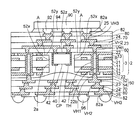
【解決手段】開口部2aを備えた基板2と、基板2に形成された配線層22と、開口部2a内に配置された電子部品40と、基板2の一方の面に形成され、電子部品40を封止する第1絶縁層50と、基板2の他方の面に形成された第2絶縁層60と、第1絶縁層50上に形成された配線層23と、第2絶縁層60上に形成された配線層23とを有し、第1絶縁層50は、基板2の一方の面を被覆して開口部2a内を充填する内側絶縁層52と、内側絶縁層52上に形成された外側絶縁層54とから形成されていることを含む。
【選択図】図10
Description
Claims (12)
- 開口部を備えた基板と、
前記基板に形成された第1配線層と、
前記開口部内に配置された電子部品と、
前記基板の一方の面に形成され、前記電子部品を封止する第1絶縁層と、
前記基板の他方の面に形成された第2絶縁層と、
前記第1絶縁層上に形成された第2配線層と、
前記第2絶縁層上に形成された第3配線層と
を有し、
前記第1絶縁層は、前記基板の一方の面を被覆して前記開口部内を充填する内側絶縁層と、前記内側絶縁層上に形成された外側絶縁層とから形成されていることを特徴とする電子部品内蔵基板。 - 前記第1配線層は、前記基板の両面にそれぞれ形成されており、
前記第2配線層が、前記内側絶縁層及び外側絶縁層内に形成されたビア導体を介して前記第1配線層に接続されており、
前記第3配線層が、前記第2絶縁層内に形成されたビア導体を介して前記電子部品の接続端子及び前記第1配線層に接続されていることを特徴とする請求項1に記載の電子部品内蔵基板。 - 前記第1絶縁層の厚みは、前記第2絶縁層の厚みと略同一であることを特徴とする請求項1又は2に記載の電子部品内蔵基板。
- 前記開口部の外側周囲領域の前記基板の表面は、前記第1配線層が後退した露出面となっており、前記露出面と前記第2絶縁層との間に、前記内側絶縁層の補強絶縁部が形成されていることを特徴とする請求項1乃至3のいずれか一項に記載の電子部品内蔵基板。
- 前記開口部に充填された部分の前記内側絶縁層に窪み部が形成されており、前記窪み部を充填して前記内側絶縁層の上に前記外側絶縁層が形成されて、前記第1絶縁層の表面が平坦化されていることを特徴とする請求項1乃至4のいずれか一項に記載の電子部品内蔵基板。
- 前記基板の前記第2絶縁層側の最外面が半導体チップを搭載する部品搭載面として形成されることを特徴とする請求項1乃至5のいずれか一項に記載の電子部品内蔵基板。
- 第1配線層を備えた基板を用意し、前記基板に開口部を形成する工程と、
前記開口部内に電子部品を配置する工程と、
前記基板の一方の面に前記電子部品を封止する内側絶縁層を形成する工程と、
前記内側絶縁層の上に外側絶縁層を形成して前記基板の一方の面に前記内側絶縁層及び外側絶縁層から形成される第1絶縁層を得ると共に、前記基板の他方の面に第2絶縁層を形成する工程と、
前記第1絶縁層の上に第2配線層を形成すると共に、前記第2絶縁層の上に第3配線層を形成する工程とを有することを電子部品内蔵基板の製造方法。 - 前記基板を用意し、開口部を形成する工程において、前記第1配線層は前記基板の両面にそれぞれ形成されており、
前記第2配線層及び第3配線層を形成する工程において
前記第2配線層は、前記第1絶縁層内に形成されたビア導体を介して前記第1配線層に接続され、
前記第3配線層は、前記第2絶縁層内に形成されたビア導体を介して前記電子部品の接続端子及び前記第1配線層に接続されることを特徴とする請求項7に記載の電子部品内蔵基板の製造方法。 - 前記第1絶縁層の厚みと前記第2絶縁層の厚みとが略同一に設定されることを特徴とする請求項7又は8に記載の電子部品内蔵基板の製造方法。
- 前記基板に開口部を形成する工程において、前記開口部の外側周囲領域の前記基板の表面が、前記第1配線層が外側に後退した露出面となるようにし、
前記内側絶縁層を形成する工程において、前記露出面の上に前記内側絶縁層の補強絶縁部が形成されることを特徴とする請求項7乃至9のいずれか一項に記載の電子部品内蔵基板の製造方法。 - 前記内側絶縁層を形成する工程において、前記開口部に充填された部分の前記内側絶縁層に窪み部が形成され、
前記外側絶縁層を形成する工程において、前記窪み部を充填して前記内側絶縁層の上に前記外側絶縁層が形成されて、前記第1絶縁層の表面が平坦化されることを特徴とする請求項7乃至10のいずれか一項に記載の電子部品内蔵基板の製造方法。 - 前記基板の前記第2絶縁層側の最外面が半導体チップを搭載する部品搭載面として形成されることを特徴とする請求項7乃至11のいずれか一項に記載の電子部品内蔵基板の製造方法。
Priority Applications (2)
| Application Number | Priority Date | Filing Date | Title |
|---|---|---|---|
| JP2013068549A JP6200178B2 (ja) | 2013-03-28 | 2013-03-28 | 電子部品内蔵基板及びその製造方法 |
| US14/221,567 US9331011B2 (en) | 2013-03-28 | 2014-03-21 | Electronic component built-in substrate and method of manufacturing the same |
Applications Claiming Priority (1)
| Application Number | Priority Date | Filing Date | Title |
|---|---|---|---|
| JP2013068549A JP6200178B2 (ja) | 2013-03-28 | 2013-03-28 | 電子部品内蔵基板及びその製造方法 |
Publications (3)
| Publication Number | Publication Date |
|---|---|
| JP2014192452A true JP2014192452A (ja) | 2014-10-06 |
| JP2014192452A5 JP2014192452A5 (ja) | 2016-01-28 |
| JP6200178B2 JP6200178B2 (ja) | 2017-09-20 |
Family
ID=51620014
Family Applications (1)
| Application Number | Title | Priority Date | Filing Date |
|---|---|---|---|
| JP2013068549A Active JP6200178B2 (ja) | 2013-03-28 | 2013-03-28 | 電子部品内蔵基板及びその製造方法 |
Country Status (2)
| Country | Link |
|---|---|
| US (1) | US9331011B2 (ja) |
| JP (1) | JP6200178B2 (ja) |
Cited By (10)
| Publication number | Priority date | Publication date | Assignee | Title |
|---|---|---|---|---|
| KR20160132763A (ko) * | 2015-05-11 | 2016-11-21 | 삼성전기주식회사 | 팬-아웃 반도체 패키지 및 그 제조방법 |
| KR20180012187A (ko) * | 2016-07-26 | 2018-02-05 | 삼성전기주식회사 | 팬-아웃 반도체 패키지 |
| JP2018064085A (ja) * | 2016-10-10 | 2018-04-19 | サムソン エレクトロ−メカニックス カンパニーリミテッド. | ファン−アウト半導体パッケージ及び感光性樹脂組成物 |
| KR20180055570A (ko) * | 2016-11-17 | 2018-05-25 | 삼성전기주식회사 | 팬-아웃 반도체 패키지 |
| US10199337B2 (en) | 2015-05-11 | 2019-02-05 | Samsung Electro-Mechanics Co., Ltd. | Electronic component package and method of manufacturing the same |
| KR20190023285A (ko) * | 2017-08-28 | 2019-03-08 | 삼성전기주식회사 | 팬-아웃 반도체 패키지 |
| US10262949B2 (en) | 2015-05-11 | 2019-04-16 | Samsung Electro-Mechanics Co., Ltd. | Fan-out semiconductor package and method of manufacturing the same |
| WO2019111873A1 (ja) * | 2017-12-05 | 2019-06-13 | 株式会社村田製作所 | モジュール |
| CN110957281A (zh) * | 2018-09-27 | 2020-04-03 | 台湾积体电路制造股份有限公司 | 集成电路封装件和方法 |
| US12074104B2 (en) | 2018-09-27 | 2024-08-27 | Taiwan Semiconductor Manufacturing Company, Ltd. | Integrated circuit packages with ring-shaped substrates |
Families Citing this family (13)
| Publication number | Priority date | Publication date | Assignee | Title |
|---|---|---|---|---|
| KR101601815B1 (ko) * | 2014-02-06 | 2016-03-10 | 삼성전기주식회사 | 임베디드 기판, 인쇄회로기판 및 그 제조 방법 |
| US9837484B2 (en) * | 2015-05-27 | 2017-12-05 | STATS ChipPAC Pte. Ltd. | Semiconductor device and method of forming substrate including embedded component with symmetrical structure |
| US10700024B2 (en) * | 2017-08-18 | 2020-06-30 | Samsung Electro-Mechanics Co., Ltd. | Fan-out semiconductor package |
| EP3474639B1 (en) * | 2017-10-20 | 2021-07-14 | AT & S Austria Technologie & Systemtechnik Aktiengesellschaft | Embedding a component into a component carrier by transferring the component into a cavity being already filled with filling material |
| KR102005351B1 (ko) * | 2017-12-07 | 2019-07-31 | 삼성전자주식회사 | 팬-아웃 센서 패키지 |
| KR102039711B1 (ko) * | 2018-03-13 | 2019-11-01 | 삼성전자주식회사 | 팬-아웃 부품 패키지 |
| US10797017B2 (en) * | 2018-03-20 | 2020-10-06 | Unimicron Technology Corp. | Embedded chip package, manufacturing method thereof, and package-on-package structure |
| CN208691627U (zh) * | 2018-08-03 | 2019-04-02 | 奥特斯科技(重庆)有限公司 | 具有嵌入腔中的部件且前侧上具有双介电层的部件承载件 |
| KR102595864B1 (ko) * | 2018-12-07 | 2023-10-30 | 삼성전자주식회사 | 반도체 패키지 |
| US10903169B2 (en) | 2019-04-30 | 2021-01-26 | Advanced Semiconductor Engineering, Inc. | Conductive structure and wiring structure including the same |
| US11145624B2 (en) * | 2019-07-26 | 2021-10-12 | Advanced Semiconductor Engineering, Inc. | Semiconductor device package and method for manufacturing the same |
| JP2021082786A (ja) * | 2019-11-22 | 2021-05-27 | ルネサスエレクトロニクス株式会社 | 半導体装置 |
| KR102854180B1 (ko) * | 2020-07-27 | 2025-09-03 | 삼성전기주식회사 | 전자부품 내장기판 |
Citations (2)
| Publication number | Priority date | Publication date | Assignee | Title |
|---|---|---|---|---|
| JP2010114434A (ja) * | 2008-10-08 | 2010-05-20 | Ngk Spark Plug Co Ltd | 部品内蔵配線基板及びその製造方法 |
| WO2010137421A1 (ja) * | 2009-05-29 | 2010-12-02 | イビデン株式会社 | 配線板及びその製造方法 |
Family Cites Families (6)
| Publication number | Priority date | Publication date | Assignee | Title |
|---|---|---|---|---|
| JP3709882B2 (ja) * | 2003-07-22 | 2005-10-26 | 松下電器産業株式会社 | 回路モジュールとその製造方法 |
| TWI324901B (en) * | 2007-01-08 | 2010-05-11 | Unimicron Technology Corp | Printed circuit board structure integrating electronic components |
| TWI363411B (en) * | 2008-07-22 | 2012-05-01 | Advanced Semiconductor Eng | Embedded chip substrate and fabrication method thereof |
| JP5001395B2 (ja) | 2010-03-31 | 2012-08-15 | イビデン株式会社 | 配線板及び配線板の製造方法 |
| US8895380B2 (en) * | 2010-11-22 | 2014-11-25 | Bridge Semiconductor Corporation | Method of making semiconductor assembly with built-in stiffener and semiconductor assembly manufactured thereby |
| US9406658B2 (en) * | 2010-12-17 | 2016-08-02 | Advanced Semiconductor Engineering, Inc. | Embedded component device and manufacturing methods thereof |
-
2013
- 2013-03-28 JP JP2013068549A patent/JP6200178B2/ja active Active
-
2014
- 2014-03-21 US US14/221,567 patent/US9331011B2/en active Active
Patent Citations (2)
| Publication number | Priority date | Publication date | Assignee | Title |
|---|---|---|---|---|
| JP2010114434A (ja) * | 2008-10-08 | 2010-05-20 | Ngk Spark Plug Co Ltd | 部品内蔵配線基板及びその製造方法 |
| WO2010137421A1 (ja) * | 2009-05-29 | 2010-12-02 | イビデン株式会社 | 配線板及びその製造方法 |
Cited By (23)
| Publication number | Priority date | Publication date | Assignee | Title |
|---|---|---|---|---|
| US10262949B2 (en) | 2015-05-11 | 2019-04-16 | Samsung Electro-Mechanics Co., Ltd. | Fan-out semiconductor package and method of manufacturing the same |
| KR20160132763A (ko) * | 2015-05-11 | 2016-11-21 | 삼성전기주식회사 | 팬-아웃 반도체 패키지 및 그 제조방법 |
| KR102002071B1 (ko) * | 2015-05-11 | 2019-07-22 | 삼성전자주식회사 | 팬-아웃 반도체 패키지 및 그 제조방법 |
| JP2018198333A (ja) * | 2015-05-11 | 2018-12-13 | サムソン エレクトロ−メカニックス カンパニーリミテッド. | ファンアウト半導体パッケージ及びその製造方法 |
| US10199337B2 (en) | 2015-05-11 | 2019-02-05 | Samsung Electro-Mechanics Co., Ltd. | Electronic component package and method of manufacturing the same |
| US10256200B2 (en) | 2015-05-11 | 2019-04-09 | Samsung Electro-Mechanics Co., Ltd. | Electronic component package and method of manufacturing the same |
| JP2016213466A (ja) * | 2015-05-11 | 2016-12-15 | サムソン エレクトロ−メカニックス カンパニーリミテッド. | ファンアウト半導体パッケージ及びその製造方法 |
| KR20180012187A (ko) * | 2016-07-26 | 2018-02-05 | 삼성전기주식회사 | 팬-아웃 반도체 패키지 |
| KR101994752B1 (ko) * | 2016-07-26 | 2019-07-01 | 삼성전기주식회사 | 팬-아웃 반도체 패키지 |
| JP2018064085A (ja) * | 2016-10-10 | 2018-04-19 | サムソン エレクトロ−メカニックス カンパニーリミテッド. | ファン−アウト半導体パッケージ及び感光性樹脂組成物 |
| US10283426B2 (en) | 2016-10-10 | 2019-05-07 | Samsung Electro-Mechanics Co., Ltd. | Fan-out semiconductor package and photosensitive resin composition |
| KR20180055570A (ko) * | 2016-11-17 | 2018-05-25 | 삼성전기주식회사 | 팬-아웃 반도체 패키지 |
| US10217631B2 (en) | 2016-11-17 | 2019-02-26 | Samsung Electro-Mechanics Co., Ltd. | Fan-out semiconductor package |
| KR102004801B1 (ko) * | 2016-11-17 | 2019-07-29 | 삼성전기주식회사 | 팬-아웃 반도체 패키지 |
| KR20190023285A (ko) * | 2017-08-28 | 2019-03-08 | 삼성전기주식회사 | 팬-아웃 반도체 패키지 |
| KR102029535B1 (ko) * | 2017-08-28 | 2019-10-07 | 삼성전기주식회사 | 팬-아웃 반도체 패키지 |
| US10685929B2 (en) | 2017-08-28 | 2020-06-16 | Samsung Electro-Mechanics Co., Ltd. | Fan-out semiconductor package |
| WO2019111873A1 (ja) * | 2017-12-05 | 2019-06-13 | 株式会社村田製作所 | モジュール |
| US11322472B2 (en) | 2017-12-05 | 2022-05-03 | Murata Manufacturing Co., Ltd. | Module |
| CN110957281A (zh) * | 2018-09-27 | 2020-04-03 | 台湾积体电路制造股份有限公司 | 集成电路封装件和方法 |
| US11527474B2 (en) | 2018-09-27 | 2022-12-13 | Taiwan Semiconductor Manufacturing Company, Ltd. | Integrated circuit package and method |
| CN110957281B (zh) * | 2018-09-27 | 2023-06-30 | 台湾积体电路制造股份有限公司 | 集成电路封装件和方法 |
| US12074104B2 (en) | 2018-09-27 | 2024-08-27 | Taiwan Semiconductor Manufacturing Company, Ltd. | Integrated circuit packages with ring-shaped substrates |
Also Published As
| Publication number | Publication date |
|---|---|
| JP6200178B2 (ja) | 2017-09-20 |
| US20140291859A1 (en) | 2014-10-02 |
| US9331011B2 (en) | 2016-05-03 |
Similar Documents
| Publication | Publication Date | Title |
|---|---|---|
| JP6200178B2 (ja) | 電子部品内蔵基板及びその製造方法 | |
| KR102032171B1 (ko) | 전자 부품 내장 기판 및 그 제조 방법 | |
| JP5395360B2 (ja) | 電子部品内蔵基板の製造方法 | |
| CN102986314B (zh) | 层叠配线基板及其制造方法 | |
| JP6208411B2 (ja) | 配線基板及びその製造方法 | |
| JP2007165888A (ja) | 電子素子内蔵印刷回路基板及びその製造方法 | |
| JP2011159855A (ja) | 局所多層回路基板、および局所多層回路基板の製造方法 | |
| JP2016134624A (ja) | 電子素子内蔵型印刷回路基板及びその製造方法 | |
| KR101205464B1 (ko) | 인쇄회로기판 제조방법 | |
| JP2010157664A (ja) | 電気・電子部品内蔵回路基板とその製造方法 | |
| WO2012128269A1 (ja) | 配線基板 | |
| JP5593863B2 (ja) | 積層回路基板および基板製造方法 | |
| JP6266908B2 (ja) | 電子部品内蔵基板の製造方法 | |
| JP6062884B2 (ja) | 部品内蔵基板及びその製造方法並びに実装体 | |
| TWI477214B (zh) | 具有內埋元件的電路板及其製作方法 | |
| KR101138542B1 (ko) | 다층 인쇄회로기판의 제조방법 | |
| JP5385699B2 (ja) | 積層配線基板の製造方法 | |
| TW201316856A (zh) | 內藏元件之基板及其製造方法 | |
| JP5836019B2 (ja) | 部品内蔵基板およびその製造方法 | |
| KR100888562B1 (ko) | 능동소자 내장형 인쇄회로기판 제조 방법 | |
| JP4899409B2 (ja) | 多層プリント配線基板及びその製造方法 | |
| JP4803918B2 (ja) | 多層配線基板の製造方法 | |
| TWI590732B (zh) | 使用封閉及內部微穿孔耦接次總成製造印刷電路板之系統及方法 | |
| JP4803919B2 (ja) | 多層配線基板の製造方法 | |
| JP6075789B2 (ja) | 配線基板の製造方法 |
Legal Events
| Date | Code | Title | Description |
|---|---|---|---|
| A521 | Request for written amendment filed |
Free format text: JAPANESE INTERMEDIATE CODE: A523 Effective date: 20151207 |
|
| A621 | Written request for application examination |
Free format text: JAPANESE INTERMEDIATE CODE: A621 Effective date: 20151207 |
|
| A977 | Report on retrieval |
Free format text: JAPANESE INTERMEDIATE CODE: A971007 Effective date: 20161027 |
|
| A131 | Notification of reasons for refusal |
Free format text: JAPANESE INTERMEDIATE CODE: A131 Effective date: 20161206 |
|
| A521 | Request for written amendment filed |
Free format text: JAPANESE INTERMEDIATE CODE: A523 Effective date: 20170117 |
|
| TRDD | Decision of grant or rejection written | ||
| A01 | Written decision to grant a patent or to grant a registration (utility model) |
Free format text: JAPANESE INTERMEDIATE CODE: A01 Effective date: 20170808 |
|
| A61 | First payment of annual fees (during grant procedure) |
Free format text: JAPANESE INTERMEDIATE CODE: A61 Effective date: 20170825 |
|
| R150 | Certificate of patent or registration of utility model |
Ref document number: 6200178 Country of ref document: JP Free format text: JAPANESE INTERMEDIATE CODE: R150 |