JP2014207295A - Semiconductor device - Google Patents
Semiconductor device Download PDFInfo
- Publication number
- JP2014207295A JP2014207295A JP2013083309A JP2013083309A JP2014207295A JP 2014207295 A JP2014207295 A JP 2014207295A JP 2013083309 A JP2013083309 A JP 2013083309A JP 2013083309 A JP2013083309 A JP 2013083309A JP 2014207295 A JP2014207295 A JP 2014207295A
- Authority
- JP
- Japan
- Prior art keywords
- insulating film
- contact
- gate electrode
- impurity diffusion
- wiring
- Prior art date
- Legal status (The legal status is an assumption and is not a legal conclusion. Google has not performed a legal analysis and makes no representation as to the accuracy of the status listed.)
- Pending
Links
- 239000004065 semiconductor Substances 0.000 title claims abstract description 230
- 239000000758 substrate Substances 0.000 claims abstract description 32
- 229910052751 metal Inorganic materials 0.000 claims abstract description 30
- 239000002184 metal Substances 0.000 claims abstract description 30
- 239000010410 layer Substances 0.000 claims description 119
- 239000012535 impurity Substances 0.000 claims description 109
- 238000009792 diffusion process Methods 0.000 claims description 93
- 239000011229 interlayer Substances 0.000 claims description 51
- 239000012212 insulator Substances 0.000 claims description 8
- 239000002131 composite material Substances 0.000 claims description 4
- 238000009413 insulation Methods 0.000 abstract description 5
- 238000002955 isolation Methods 0.000 description 42
- XUIMIQQOPSSXEZ-UHFFFAOYSA-N Silicon Chemical compound [Si] XUIMIQQOPSSXEZ-UHFFFAOYSA-N 0.000 description 41
- 229910052710 silicon Inorganic materials 0.000 description 41
- 239000010703 silicon Substances 0.000 description 41
- 238000000034 method Methods 0.000 description 32
- VYPSYNLAJGMNEJ-UHFFFAOYSA-N Silicium dioxide Chemical group O=[Si]=O VYPSYNLAJGMNEJ-UHFFFAOYSA-N 0.000 description 19
- 229910052814 silicon oxide Inorganic materials 0.000 description 19
- 238000005229 chemical vapour deposition Methods 0.000 description 18
- 239000010936 titanium Substances 0.000 description 13
- RTAQQCXQSZGOHL-UHFFFAOYSA-N Titanium Chemical compound [Ti] RTAQQCXQSZGOHL-UHFFFAOYSA-N 0.000 description 11
- 230000015572 biosynthetic process Effects 0.000 description 11
- 229910052719 titanium Inorganic materials 0.000 description 11
- 238000004519 manufacturing process Methods 0.000 description 10
- 229910052581 Si3N4 Inorganic materials 0.000 description 9
- HQVNEWCFYHHQES-UHFFFAOYSA-N silicon nitride Chemical group N12[Si]34N5[Si]62N3[Si]51N64 HQVNEWCFYHHQES-UHFFFAOYSA-N 0.000 description 9
- PXHVJJICTQNCMI-UHFFFAOYSA-N Nickel Chemical compound [Ni] PXHVJJICTQNCMI-UHFFFAOYSA-N 0.000 description 7
- 238000001312 dry etching Methods 0.000 description 7
- 238000000206 photolithography Methods 0.000 description 7
- NRTOMJZYCJJWKI-UHFFFAOYSA-N Titanium nitride Chemical compound [Ti]#N NRTOMJZYCJJWKI-UHFFFAOYSA-N 0.000 description 5
- 238000005530 etching Methods 0.000 description 5
- 230000000149 penetrating effect Effects 0.000 description 5
- 230000002093 peripheral effect Effects 0.000 description 5
- 229920002120 photoresistant polymer Polymers 0.000 description 5
- WFKWXMTUELFFGS-UHFFFAOYSA-N tungsten Chemical compound [W] WFKWXMTUELFFGS-UHFFFAOYSA-N 0.000 description 5
- 229910052721 tungsten Inorganic materials 0.000 description 5
- 239000010937 tungsten Substances 0.000 description 5
- ZOXJGFHDIHLPTG-UHFFFAOYSA-N Boron Chemical compound [B] ZOXJGFHDIHLPTG-UHFFFAOYSA-N 0.000 description 4
- 229910052785 arsenic Inorganic materials 0.000 description 4
- RQNWIZPPADIBDY-UHFFFAOYSA-N arsenic atom Chemical compound [As] RQNWIZPPADIBDY-UHFFFAOYSA-N 0.000 description 4
- 229910052796 boron Inorganic materials 0.000 description 4
- 239000007772 electrode material Substances 0.000 description 4
- 230000003647 oxidation Effects 0.000 description 4
- 238000007254 oxidation reaction Methods 0.000 description 4
- OAICVXFJPJFONN-UHFFFAOYSA-N Phosphorus Chemical compound [P] OAICVXFJPJFONN-UHFFFAOYSA-N 0.000 description 3
- 238000010438 heat treatment Methods 0.000 description 3
- 238000005468 ion implantation Methods 0.000 description 3
- 239000012528 membrane Substances 0.000 description 3
- 229910052698 phosphorus Inorganic materials 0.000 description 3
- 239000011574 phosphorus Substances 0.000 description 3
- 229910021420 polycrystalline silicon Inorganic materials 0.000 description 3
- 230000008569 process Effects 0.000 description 3
- 238000004544 sputter deposition Methods 0.000 description 3
- IVHJCRXBQPGLOV-UHFFFAOYSA-N azanylidynetungsten Chemical compound [W]#N IVHJCRXBQPGLOV-UHFFFAOYSA-N 0.000 description 2
- 238000006243 chemical reaction Methods 0.000 description 2
- 239000010941 cobalt Substances 0.000 description 2
- 229910017052 cobalt Inorganic materials 0.000 description 2
- GUTLYIVDDKVIGB-UHFFFAOYSA-N cobalt atom Chemical compound [Co] GUTLYIVDDKVIGB-UHFFFAOYSA-N 0.000 description 2
- ZOCHARZZJNPSEU-UHFFFAOYSA-N diboron Chemical compound B#B ZOCHARZZJNPSEU-UHFFFAOYSA-N 0.000 description 2
- 230000000694 effects Effects 0.000 description 2
- 238000009434 installation Methods 0.000 description 2
- 150000002500 ions Chemical class 0.000 description 2
- 239000007769 metal material Substances 0.000 description 2
- 229910052759 nickel Inorganic materials 0.000 description 2
- 229910021332 silicide Inorganic materials 0.000 description 2
- FVBUAEGBCNSCDD-UHFFFAOYSA-N silicide(4-) Chemical compound [Si-4] FVBUAEGBCNSCDD-UHFFFAOYSA-N 0.000 description 2
- 229910021341 titanium silicide Inorganic materials 0.000 description 2
- 239000012808 vapor phase Substances 0.000 description 2
- 238000001039 wet etching Methods 0.000 description 2
- XYFCBTPGUUZFHI-UHFFFAOYSA-N Phosphine Chemical compound P XYFCBTPGUUZFHI-UHFFFAOYSA-N 0.000 description 1
- BLRPTPMANUNPDV-UHFFFAOYSA-N Silane Chemical compound [SiH4] BLRPTPMANUNPDV-UHFFFAOYSA-N 0.000 description 1
- 230000004888 barrier function Effects 0.000 description 1
- 230000015556 catabolic process Effects 0.000 description 1
- 230000000295 complement effect Effects 0.000 description 1
- 239000004020 conductor Substances 0.000 description 1
- 239000013078 crystal Substances 0.000 description 1
- 230000003247 decreasing effect Effects 0.000 description 1
- 238000000151 deposition Methods 0.000 description 1
- 238000010586 diagram Methods 0.000 description 1
- 239000007789 gas Substances 0.000 description 1
- 238000002513 implantation Methods 0.000 description 1
- 239000000463 material Substances 0.000 description 1
- 150000002739 metals Chemical class 0.000 description 1
- 238000012986 modification Methods 0.000 description 1
- 230000004048 modification Effects 0.000 description 1
- 230000001590 oxidative effect Effects 0.000 description 1
- 238000005498 polishing Methods 0.000 description 1
- 230000009467 reduction Effects 0.000 description 1
- 239000000126 substance Substances 0.000 description 1
- MZLGASXMSKOWSE-UHFFFAOYSA-N tantalum nitride Chemical compound [Ta]#N MZLGASXMSKOWSE-UHFFFAOYSA-N 0.000 description 1
Images







Landscapes
- Semiconductor Memories (AREA)
- Metal-Oxide And Bipolar Metal-Oxide Semiconductor Integrated Circuits (AREA)
Abstract
Description
本発明は、半導体装置に関し、特に縦型トランジスタを用いる半導体装置に関する。 The present invention relates to a semiconductor device, and more particularly to a semiconductor device using a vertical transistor.
半導体装置、特にメモリデバイスのチップサイズは、低コストの観点から年々縮小されている。これに応じ、DRAM(Dynamic Random Access Memory)では、セルトランジスタ用として4F2構造を有する縦型トランジスタの採用が進められている(例えば特許文献1,2参照)。
The chip size of semiconductor devices, particularly memory devices, is decreasing year by year from the viewpoint of low cost. Depending on this, DRAM in (Dynamic Random Access Memory), (see for example,
縦型トランジスタは、チャネルが半導体基板主面の法線方向に延設されるトランジスタである。具体的には、半導体基板の主面に立設された半導体ピラーの上部にソース領域/ドレイン領域の一方、下部にソース領域/ドレイン領域の他方がそれぞれ設けられ、ゲート電極が半導体ピラーの側面全周を取り囲むという構成を有している。縦型トランジスタを用いる場合、チャネル長が平面的な占有面積に左右されず、微細化が進んでも十分なチャネル長を確保することができるので、短チャネル効果の抑制、チャネルの完全空乏化、良好なS値(Subthreshold swing value)、大きなドレイン電流、といった数々のメリットが得られる。 The vertical transistor is a transistor whose channel extends in the normal direction of the main surface of the semiconductor substrate. Specifically, one of the source region / drain region is provided on the upper side of the semiconductor pillar standing on the main surface of the semiconductor substrate, and the other of the source region / drain region is provided on the lower side. It has a configuration of surrounding the circumference. When a vertical transistor is used, the channel length does not depend on the planar occupation area, and a sufficient channel length can be secured even if miniaturization progresses, so the short channel effect is suppressed, the channel is fully depleted, and good Numerous merits such as a large S value (Subthreshold swing value) and a large drain current can be obtained.
周辺回路のトランジスタ用としては、セルトランジスタほど縮小化の要請がないことから従来のプレーナー型トランジスタが引き続き採用されている。しかし、セルと周辺回路とでトランジスタの構造が異なると工程数が大幅に増大してしまうことから、最近では、周辺回路のトランジスタにも4F2構造を有する縦型トランジスタの採用が検討されている(例えば特許文献3参照) As a peripheral circuit transistor, a conventional planar transistor has been continuously adopted because there is no demand for reduction as much as a cell transistor. However, if the structure of the transistor is different between the cell and the peripheral circuit, the number of processes increases significantly. Therefore, recently, the use of a vertical transistor having a 4F 2 structure is also considered for the transistor of the peripheral circuit. (For example, see Patent Document 3)
周辺回路に設置される縦型トランジスタでは、特許文献3に記載されているように、2種類の半導体ピラーが用いられる。一方の種類の半導体ピラーはチャネルとして用いられるもので、上部及び下部それぞれに不純物拡散層が設けられ、側面はゲート絶縁膜を介してゲート電極に覆われている。ゲート電極として具体的には、導電性のシリコン膜(CVD(Chemical Vapor Deposition)法により不純物ドープシリコン膜として形成したもの)を成膜した後、これをエッチバックすることにより得られるサイドウォール状のシリコン膜が用いられる。シリコン膜には比抵抗が大きいという難があるが、比抵抗の小さい金属材料は結晶性が高く、エッチバックによる形成ではゲート電極上面を均一に構成することが困難であることから、今のところシリコン膜が利用されている。他方の種類の半導体ピラーは、サイドウォール状のシリコン膜であるゲート電極の長さを横方向に延長するためのダミーピラーであり、延長された部分を利用してゲートコンタクトプラグが設けられる。
In the vertical transistor installed in the peripheral circuit, as described in
ところで、DRAMの周辺回路では、素子分離領域を挟んで隣接する活性領域に各々配置された縦型トランジスタのゲート電極を互いに接続する場合がある。この場合、これまでは、素子分離領域を横断するダミーピラーを設けることによりサイドウォール状のシリコン膜で接続する方法や、それぞれのゲート電極を上述したゲートコンタクトプラグによって上層配線に引き出して上層配線で接続する方法が取られている。 By the way, in the peripheral circuit of the DRAM, there are cases where the gate electrodes of the vertical transistors respectively disposed in the active regions adjacent to each other with the element isolation region interposed therebetween are connected to each other. In this case, until now, a dummy pillar that traverses the element isolation region is used to connect with a sidewall-like silicon film, or each gate electrode is connected to the upper layer wiring by the gate contact plug described above and connected to the upper layer wiring. The way to do is taken.
しかしながら、いずれの方法にも、ゲート電極間の配線抵抗が大きくなってしまうという問題がある。前者の方法については、シリコン膜が高い抵抗値を有する(金属膜材料に比べて2桁程度高い)ためであり、後者の方法については、ゲートコンタクトプラグを経由する分の配線抵抗が加算されるためである。 However, both methods have a problem that the wiring resistance between the gate electrodes increases. This is because the silicon film has a high resistance value (about two orders of magnitude higher than that of the metal film material) in the former method, and in the latter method, the wiring resistance through the gate contact plug is added. Because.
本発明による半導体装置は、主面に第1及び第2の活性領域が区画された半導体基板と、前記第1の活性領域に立設された第1の半導体ピラーと、前記第2の活性領域に立設された第2の半導体ピラーと、ゲート絶縁膜を介して前記第1の半導体ピラーの側面を覆う第1のゲート電極と、ゲート絶縁膜を介して前記第2の半導体ピラーの側面を覆う第2のゲート電極と、前記第1の半導体ピラーの上端に設けられた第1の上部不純物拡散層と、前記第2の半導体ピラーの上端に設けられた第2の上部不純物拡散層と、前記第1の半導体ピラーの下部に接して設けられた第1の下部不純物拡散層と、前記第2の半導体ピラーの下部に接して設けられた第2の下部不純物拡散層と、前記主面のうち前記第1及び第2の活性領域の間に配置されて前記第1のゲート電極と前記第2のゲート電極とを分離する一方、前記第1及び第2のゲート電極それぞれの上端が上面から突出する膜厚で形成された埋設絶縁膜と、前記埋設絶縁膜の上面に形成され、下面の一端で前記第1のゲート電極の上端と接触し、下面の他端で前記第2のゲート電極の上端と接触する金属膜とを備えることを特徴とする。 The semiconductor device according to the present invention includes a semiconductor substrate in which a first active region and a second active region are partitioned on a main surface, a first semiconductor pillar standing on the first active region, and the second active region. A second semiconductor pillar erected on the first side, a first gate electrode covering the side surface of the first semiconductor pillar via a gate insulating film, and a side surface of the second semiconductor pillar via a gate insulating film A second gate electrode covering, a first upper impurity diffusion layer provided on an upper end of the first semiconductor pillar, a second upper impurity diffusion layer provided on an upper end of the second semiconductor pillar, A first lower impurity diffusion layer provided in contact with a lower portion of the first semiconductor pillar; a second lower impurity diffusion layer provided in contact with a lower portion of the second semiconductor pillar; Before being disposed between the first and second active regions A buried insulating film that separates the first gate electrode and the second gate electrode, and has a thickness that protrudes from an upper surface of each of the first and second gate electrodes; and the buried insulating film And a metal film in contact with the upper end of the first gate electrode at one end of the lower surface and in contact with the upper end of the second gate electrode at the other end of the lower surface.
本発明の他の一側面による半導体装置は、主面に第1及び第2の活性領域が区画された半導体基板と、それぞれ前記第1の活性領域に立設された複数の第1の半導体ピラーと、それぞれ前記第2の活性領域に立設された複数の第2の半導体ピラーと、ゲート絶縁膜を介して前記複数の第1の半導体ピラーの側面を覆う第1のゲート電極と、ゲート絶縁膜を介して前記複数の第2の半導体ピラーの側面を覆う第2のゲート電極と、それぞれ前記複数の第1の半導体ピラーの上端に設けられた複数の第1の上部不純物拡散層と、それぞれ前記複数の第2の半導体ピラーの上端に設けられた複数の第2の上部不純物拡散層と、前記複数の第1の半導体ピラーそれぞれの下部に接して設けられた第1の下部不純物拡散層と、前記複数の第2の半導体ピラーそれぞれの下部に接して設けられた第2の下部不純物拡散層と、前記主面のうち前記第1及び第2の活性領域の間に配置されて前記第1のゲート電極と前記第2のゲート電極とを分離する一方、前記第1及び第2のゲート電極それぞれの上端が上面から突出する膜厚で形成された埋設絶縁膜と、前記埋設絶縁膜の上面に形成され、下面の一端で前記第1のゲート電極の上端と接触し、下面の他端で前記第2のゲート電極の上端と接触する金属膜とを備えることを特徴とする。 A semiconductor device according to another aspect of the present invention includes a semiconductor substrate having first and second active regions defined on a main surface, and a plurality of first semiconductor pillars erected on the first active region, respectively. A plurality of second semiconductor pillars standing on the second active region, a first gate electrode covering the side surfaces of the plurality of first semiconductor pillars via a gate insulating film, and gate insulation A second gate electrode that covers the side surfaces of the plurality of second semiconductor pillars through a film, a plurality of first upper impurity diffusion layers provided at upper ends of the plurality of first semiconductor pillars, respectively; A plurality of second upper impurity diffusion layers provided at upper ends of the plurality of second semiconductor pillars; a first lower impurity diffusion layer provided in contact with the lower portions of the plurality of first semiconductor pillars; , The plurality of second semiconductor pins. A second lower impurity diffusion layer provided in contact with each lower portion and the first gate electrode and the second second electrode disposed between the first and second active regions of the main surface. While separating the gate electrode, the upper end of each of the first and second gate electrodes is formed with a film thickness protruding from the upper surface, and formed on the upper surface of the embedded insulating film, and at one end of the lower surface And a metal film in contact with the upper end of the first gate electrode and in contact with the upper end of the second gate electrode at the other end of the lower surface.
本発明のさらに他の一側面による半導体装置は、第1の導電型である第1の活性領域、及び、前記第1の導電型とは異なる第2の導電型である第2の活性領域が主面に区画された半導体基板と、それぞれ前記第1の活性領域に立設された複数の第1の半導体ピラーと、それぞれ前記第2の活性領域に立設された複数の第2の半導体ピラーと、ゲート絶縁膜を介して前記複数の第1の半導体ピラーの側面を覆う第1のゲート電極と、ゲート絶縁膜を介して前記複数の第2の半導体ピラーの側面を覆う第2のゲート電極と、それぞれ前記複数の第1の半導体ピラーの上端に設けられた複数の第1の上部不純物拡散層と、それぞれ前記複数の第2の半導体ピラーの上端に設けられた複数の第2の上部不純物拡散層と、前記複数の第1の半導体ピラーそれぞれの下部に接して設けられた第1の下部不純物拡散層と、前記複数の第2の半導体ピラーそれぞれの下部に接して設けられた第2の下部不純物拡散層と、前記主面のうち前記第1及び第2の活性領域の間に配置されて前記第1のゲート電極と前記第2のゲート電極とを分離する一方、前記第1及び第2のゲート電極それぞれの上端が上面から突出する膜厚で形成された埋設絶縁膜と、前記埋設絶縁膜の上面に形成され、下面の一端で前記第1のゲート電極の上端と接触し、下面の他端で前記第2のゲート電極の上端と接触する金属膜とを備え、前記複数の第1の上部不純物拡散層の一部と、前記複数の第2の上部不純物拡散層の一部とは、互いに電気的に接続されることを特徴とする。 According to still another aspect of the present invention, there is provided a semiconductor device including: a first active region having a first conductivity type; and a second active region having a second conductivity type different from the first conductivity type. A semiconductor substrate partitioned on a main surface, a plurality of first semiconductor pillars each standing on the first active region, and a plurality of second semiconductor pillars respectively standing on the second active region A first gate electrode that covers the side surfaces of the plurality of first semiconductor pillars via a gate insulating film, and a second gate electrode that covers the side surfaces of the plurality of second semiconductor pillars via a gate insulating film A plurality of first upper impurity diffusion layers provided at the upper ends of the plurality of first semiconductor pillars, respectively, and a plurality of second upper impurities provided at the upper ends of the plurality of second semiconductor pillars, respectively. Diffusion layer and the plurality of first semiconductor pillars A first lower impurity diffusion layer provided in contact with each lower portion; a second lower impurity diffusion layer provided in contact with a lower portion of each of the plurality of second semiconductor pillars; and Of these, the first gate electrode and the second gate electrode are separated from each other by being disposed between the first and second active regions, and the upper ends of the first and second gate electrodes are separated from the upper surface. A buried insulating film formed with a protruding film thickness, formed on the upper surface of the buried insulating film, in contact with the upper end of the first gate electrode at one end of the lower surface, and the second gate electrode at the other end of the lower surface And a part of the plurality of first upper impurity diffusion layers and a part of the plurality of second upper impurity diffusion layers are electrically connected to each other. It is characterized by.
本発明によれば、第1及び第2のゲート電極が、これらを分離する埋設絶縁膜の上面に形成され、かつ、それぞれの上端と直接接触する金属膜によって互いに接続されるので、素子分離領域にもダミーピラーを設けることによりサイドウォール状のシリコン膜で接続する方法や、それぞれのゲート電極を上述したゲートコンタクトプラグによって上層配線に引き出して上層配線で接続する方法に比べて、第1のゲート電極と第2のゲート電極の間の配線抵抗を小さくすることが可能になる。 According to the present invention, the first and second gate electrodes are formed on the upper surface of the buried insulating film that separates them, and are connected to each other by the metal film that is in direct contact with the respective upper ends. In addition, the first gate electrode is compared with a method in which a dummy pillar is provided to connect with a sidewall-like silicon film, or a method in which each gate electrode is drawn to an upper layer wiring by the gate contact plug described above and connected to the upper layer wiring. The wiring resistance between the first gate electrode and the second gate electrode can be reduced.
以下、添付図面を参照しながら、本発明の好ましい実施の形態について詳細に説明する。 Hereinafter, preferred embodiments of the present invention will be described in detail with reference to the accompanying drawings.
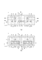
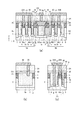
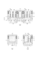
まず、図1(a)(b)及び図2(a)〜(c)を参照しながら、本発明の第1の実施の形態による半導体装置1の構造について説明する。なお、以下に示す各図においては、各構成を分かりやすく描画した結果、縮尺や数などの面で実際の構成とは異なっている部分がある。また、各図に示すZ方向は半導体基板の主面に垂直な方向であり、X方向はZ方向と直交する方向であり、Y方向はX方向及びZ方向と直交する方向である。
First, the structure of the
本実施の形態に係る半導体装置1はDRAMであり、図2(a)〜(c)に示すように、例えば不純物を加えてp型としたシリコン単結晶からなる半導体基板2を備えている。半導体基板2の主面には、図1(b)及び図2(a)〜(c)に示すように、トレンチTが設けられる。トレンチTはX方向に長い長方形の平面形状を有しており、その周囲は、STI(Shallow Trench Isolation)法による素子分離領域を構成する素子分離用絶縁膜3によって囲まれている。トレンチTの底面のうちX方向の中央付近に位置する部分には素子分離用絶縁膜3の一部を構成する素子分離用絶縁膜3aが埋め込まれており、これにより、トレンチT内のX方向一端側の領域及びX方向他端側の領域に、それぞれ第1及び第2の活性領域1A,1Bが区画されている。第1及び第2の活性領域1A,1Bは、素子分離用絶縁膜3aを挟んでX方向に隣接している。
The
なお、各図及び以下の説明から理解されるように、第1及び第2の活性領域1A,1B内の構造は、素子分離用絶縁膜3aを挟んで互いに線対称となっている。ただし、このような構造は必須ではなく、第2の実施の形態として後に詳しく説明する例のように、第1及び第2の活性領域1A,1B内の構造が線対称の関係になっていなくてもよい。
As can be understood from the drawings and the following description, the structures in the first and second
トレンチTの底面には、図1(b)及び図2(a)(c)に示すように、第1の活性領域1Aに対応して、第1−1の半導体ピラー6A1、第1−2の半導体ピラー6A2、及び第1のダミーピラー7Aとが立設されている。また、第2の活性領域1Bに対応して、第2−1の半導体ピラー6B1、第2−2の半導体ピラー6B2、及び第2のダミーピラー7Bが立設されている。以下の説明で「各ピラー」という場合、これらのピラーを指す。また、以下の説明では、第1−1の半導体ピラー6A1及び第1−2の半導体ピラー6A2をまとめて「第1の半導体ピラー」と称し、第2−1の半導体ピラー6B1及び第2−2の半導体ピラー6B2をまとめて「第2の半導体ピラー」と称する場合がある。
On the bottom surface of the trench T, as shown in FIGS. 1B and 2A and 2C, corresponding to the first
詳しくは後述するが、各ピラーは、半導体基板2に素子分離用絶縁膜3を埋め込んだ後、トレンチTと同時に形成される。つまり、まず半導体基板2の表面にシリコン酸化膜である素子分離用絶縁膜3を埋め込んで表面を平坦化した後、シリコン酸化膜であるパッド絶縁膜4とシリコン窒化膜であるマスク膜5とを順次成膜し、さらにフォトリソグラフィ法を用いて、これらをトレンチTの形状にパターニングする。このとき、各ピラーを形成する領域にもマスク膜5を残すようにする。これにより、マスク膜5をマスクとして半導体基板2及び素子分離用絶縁膜3をエッチングすることによりトレンチTを作ると、同時に各ピラーが形成されることになる。このときに用いたパッド絶縁膜4及びマスク膜5は、図2(a)〜(c)に示すように、素子分離用絶縁膜3のうちトレンチTの周囲を取り囲む部分(素子分離用絶縁膜3a以外の部分)の上面と、ダミーピラー6の上面とに残存している。パッド絶縁膜4及びマスク膜5は、後述するゲート電極11の上面の高さを各ピラーの上面より高い位置まで嵩上げし、ゲート電極11の上面と後述する配線42との距離を小さくするための突起層としても機能する。
As will be described in detail later, each pillar is formed simultaneously with the trench T after the element
第1の半導体ピラー6A1,6A2及び第2の半導体ピラー6B1,6B2は、いずれも全体が半導体基板2によって構成されており、第1の半導体ピラー6A1,6A2は素子分離用絶縁膜3aに近い側から第1−1の半導体ピラー6A1、第1−2の半導体ピラー6A2の順で、第2の半導体ピラー6B1,6B2は素子分離用絶縁膜3aに近い側から第2−1の半導体ピラー6B1、第2−2の半導体ピラー6B2の順で、それぞれX方向に並べて配置されている。したがって、第1−1の半導体ピラー6A1と第2−1の半導体ピラー6B1とは、平面的に見て、素子分離用絶縁膜3aを挟んで互いに対向している。
The
一方、第1及び第2のダミーピラー7A,7Bはそれぞれ、半導体基板2からなる半導体ピラー7a(ダミー半導体ピラー)と、素子分離用絶縁膜3aからなる絶縁体ピラー7b(ダミー絶縁体ピラー)とが合体した構造を有する複合ピラーとされている。この構造は、上述したマスク膜5をパターニングする際、第1及び第2のダミーピラー7A,7B形成用のパターンを素子分離用絶縁膜3aと各活性領域との境界に設けることによって実現される。第1のダミーピラー7Aと、第2のダミーピラー7Bとは、後述する埋設絶縁膜12を挟んで互いに対向している。
On the other hand, each of the first and
なお、図1(b)では、各ピラーのそれぞれを平面形状が正方形である四角柱として描いているが、柱状であればよく、平面形状は例えば長方形、角丸長方形、円形などであってもよい。各ピラーそれぞれの平面的な大きさ(正方形である場合には一辺の長さ。円形である場合には直径)は、例えば50nmとする。第1の半導体ピラー6A1,6A2及び第2の半導体ピラー6B1,6B2の平面的な大きさを50nm以下とすることで、これらを完全空乏化することが可能になる。
In FIG. 1B, each pillar is depicted as a quadrangular prism having a square planar shape. However, the pillar shape may be any shape, and the planar shape may be, for example, a rectangle, a rounded rectangle, or a circle. Good. The planar size of each pillar (the length of one side in the case of a square or the diameter in the case of a circle) is, for example, 50 nm. By setting the planar sizes of the
第1の半導体ピラー6A1,6A2及び第2の半導体ピラー6B1,6B2それぞれの上端には、上部不純物拡散層16が形成される。また、第1及び第2の活性領域1A,1B内に位置する半導体基板2の表面のうち、各ピラーが形成されている領域を除く部分には、各ピラーの下部に接する下部不純物拡散層9が形成される。これらはいずれも、p型の半導体基板2にn型の不純物イオンを注入することにより形成される。下部不純物拡散層9の上面には、シリコン酸化膜である底絶縁膜8が形成されている。
An upper
各ピラーの側面は、導電性のシリコン膜(n型不純物含有シリコン膜)であるゲート電極11によって覆われている。ただし、第1の半導体ピラー6A1,6A2、第2の半導体ピラー6B1,6B2、及び、第1及び第2のダミーピラー7A,7Bのそれぞれを構成する半導体ピラー7aに関しては、側面とゲート電極11との間に、半導体基板2を熱酸化することによって作られるゲート絶縁膜10が配置されている。ゲート電極11の横方向の膜厚は、20nmとすることが好適である。ゲート電極11と下部不純物拡散層9とは、底絶縁膜8によって絶縁されている。
The side surface of each pillar is covered with a
各ピラーの配置間隔(X方向の表面間距離)は、第1及び第2の活性領域1A,1Bのそれぞれにおいて、各ピラーの側面に形成されるゲート電極11が一体化する値に設定される。具体的な例を挙げて説明すると、例えば上記のようにゲート電極11の横方向の膜厚を20nmとした場合には、上記配置間隔を40nm(=20nmの2倍)以下の値、例えば30nmに設定することにより、各ピラーの側面に形成されるゲート電極11を、活性領域ごとに一体化することができる。半導体装置1では、このように上記配置間隔を設定した結果、第1及び第2の活性領域1A,1Bのそれぞれにおいて、各ピラーの側面に形成されるゲート電極11は一体化されており、互いに短絡している。
The arrangement interval (distance between surfaces in the X direction) of each pillar is set to a value in which the
トレンチTの内部には、図2(a)などに示すように、マスク膜5の上面の高さまで、シリコン酸化膜である埋設絶縁膜12(埋設絶縁膜)が埋め込まれている。第1の活性領域1A内のゲート電極11(第1のゲート電極)と、第2の活性領域1B内のゲート電極11(第2のゲート電極)とは、この埋設絶縁膜12によって分離されている。
As shown in FIG. 2A and the like, a buried insulating film 12 (buried insulating film), which is a silicon oxide film, is buried in the trench T up to the height of the upper surface of the
ただし、素子分離用絶縁膜3aを挟んで対向する2つのダミーピラー6の間の領域では、埋設絶縁膜12のZ方向の膜厚が、埋設絶縁膜12の上面の位置がゲート電極11の上面より低くなるように設定される。詳しくは後述するが、この膜厚は、埋設絶縁膜12とその上面に形成された層間絶縁膜20とに、図1(b)及び図2(a)(b)に示したゲート給電コンタクト孔O3を設けることによって実現される。これにより、ゲート給電コンタクト孔O3の内部では、ゲート電極11の上端が埋設絶縁膜12の上面から突出している。
However, in the region between the two dummy pillars 6 facing each other across the element
ゲート給電コンタクト孔O3の内部には、チタン(Ti)膜、窒化チタン(TiN)膜、タングステン(W)膜を順に積層した金属膜である給電コンタクトプラグ41が埋め込まれている。給電コンタクトプラグ41は、Y方向に延在する下面の一端で第1の活性領域1Aに対応するゲート電極11(第1のダミーピラー7Aを構成する絶縁体ピラー7bの側面に形成された部分)の上端と接し、下面の他端で第2の活性領域1Bに対応するゲート電極11(第2のダミーピラー7Bを構成する絶縁体ピラー7bの側面に形成された部分)の上端と接している。したがって、第1の活性領域1A内のゲート電極11と第2の活性領域1B内のゲート電極11とは、給電コンタクトプラグ41を通じて短絡している。
A power
なお、ゲート給電コンタクト孔O3を形成する際には、ゲート電極11と給電コンタクトプラグ41の接触面積を最大化するため、第1及び第2のダミーピラー7A,7Bそれぞれの上面に残存するマスク膜5の一部分が底面に露出するようにしている。その結果として、ゲート給電コンタクト孔O3を埋める給電コンタクトプラグ41の下面の一端は、平面的に見て第1のダミーピラー7Aと重なる位置にも配置されている。同様に、ゲート給電コンタクト孔O3を埋める給電コンタクトプラグ41の下面の他端は、平面的に見て第2のダミーピラー7Bと重なる位置にも配置されている。
When forming the gate power supply contact hole O3, the
また、給電コンタクトプラグ41の最下層にチタン膜を配置するのは、シリコン膜からなるゲート電極11との接触抵抗を低減するためである。シリコン膜と接しているチタン膜はチタンシリサイド膜を構成し、これにより、給電コンタクトプラグ41とゲート電極11との接触抵抗が低減される。チタン膜に代え、コバルト(Co)膜やニッケル(Ni)膜など他のシリサイド形成金属を用いて給電コンタクトプラグ41の最下層を構成してもよく、そうすることによっても同様の接触抵抗低減効果が得られる。また、チタン膜の上層に位置する窒化チタン膜に代え、窒化タングステン(WN)膜や窒化タンタル(TaN)膜など他のバリア膜を用いてもよい。
The reason why the titanium film is disposed in the lowermost layer of the power
第1の半導体ピラー6A1,6A2及び第2の半導体ピラー6B1,6B2それぞれの上面ではパッド絶縁膜4及びマスク膜5は取り除かれており、その代わりに導電膜であるシリコンプラグ19が設けられている。シリコンプラグ19は、シリコンを成膜し、その中にヒ素等の不純物を注入(拡散)することによって形成される。シリコンプラグ19の側面は絶縁膜17及びサイドウォール膜18で覆われており、これらによってシリコンプラグ19とゲート電極11との間が絶縁されている。各シリコンプラグ19の下面は、対応する半導体ピラーの上端に設けられた上部不純物拡散層16と導通している。
The
マスク膜5、埋設絶縁膜12、及びシリコンプラグ19の上面には、上述した層間絶縁膜20が形成される。層間絶縁膜20の上面にはさらに層間絶縁膜24が形成され、層間絶縁膜24の上面には配線33A,33B,34A,34B,42(第1乃至第5の配線)を含む配線層が形成される。これらの各配線(上層配線)は、金属材料によって構成されるメタル配線である。
The above-described
配線33Aは、層間絶縁膜20,24を貫通するコンタクトプラグ30(第1のコンタクトプラグ)により、第1の半導体ピラー6A1,6A2それぞれの上面に形成された2つのシリコンプラグ19それぞれの上面と共通に接続される。配線33Bも同様であり、層間絶縁膜24,20を貫通するコンタクトプラグ30(第2のコンタクトプラグ)により、第2の半導体ピラー6B1,6B2それぞれの上面に形成された2つのシリコンプラグ19それぞれの上面と共通に接続される。
The
配線34Aは、層間絶縁膜24,20、埋設絶縁膜12、及び底絶縁膜8を貫通するコンタクトプラグ31(第3のコンタクトプラグ)により、第1の活性領域1A内の下部不純物拡散層9に接続される。配線34Bも同様であり、層間絶縁膜24,20、埋設絶縁膜12、及び底絶縁膜8を貫通するコンタクトプラグ31(第4のコンタクトプラグ)により、第2の活性領域1B内の下部不純物拡散層9に接続される。なお、これらのコンタクトプラグ31の具体的な設置領域は特に制限されないが、図1(b)に示すように、第1−1の半導体ピラー6A1及び第2−1の半導体ピラー6B1のそれぞれとY方向に隣接する位置に設置することが好ましい。
The
配線42は、層間絶縁膜24を貫通するコンタクトプラグ35(第5のコンタクトプラグ)により、給電コンタクトプラグ41の上面に接続される。
The
以上の構成により、第1の活性領域1Aに、それぞれ第1の半導体ピラー6A1,6A2をチャネル領域とする2つの縦型MOSトランジスタが形成される。同様に、第2の活性領域1Bに、それぞれ第2の半導体ピラー6B1,6B2をチャネル領域とする2つの縦型MOSトランジスタが形成される。上部不純物拡散層16及びシリコンプラグ19は各MOSトランジスタのソース/ドレインの一方を構成し、下部不純物拡散層9は各MOSトランジスタのソース/ドレインの他方を構成する。第1の活性領域1Aに形成される2つのMOSトランジスタは、それぞれの上部不純物拡散層16が共通の配線33Aに接続されており、また下部不純物拡散層9が共通であることから、配線33Aと配線34Aとの間に並列に接続され一つの第1並列トランジスタを構成している。第2の活性領域1Bに形成される2つのMOSトランジスタについても同様であり、配線33Bと配線34Bとの間に並列に接続され一つの第2並列トランジスタを構成している。
With the above configuration, two vertical MOS transistors each having the
以上説明したように、本実施の形態による半導体装置1によれば、第1の活性領域1A内のゲート電極11と、第2の活性領域1B内のゲート電極11とが、これらを分離する埋設絶縁膜12の上面に形成され、かつ、それぞれの上端と直接接触する金属膜である給電コンタクトプラグ41によって互いに接続される。したがって、素子分離領域にもダミーピラーを設けることによりサイドウォール状のシリコン膜で接続する方法や、それぞれのゲート電極をゲートコンタクトプラグによって上層配線に引き出して上層配線で接続する方法に比べて、各活性領域に形成されたゲート電極11の間の配線抵抗を小さくすることが可能になる。
As described above, according to the
また、素子分離領域を横断するダミーピラーが不要になるので、構造が簡単になり、製造工程での歩留まりが向上する。さらに、金属膜は容易にパターニングできることから、各活性領域に形成されたゲート電極11の接続に金属膜である給電コンタクトプラグ41を用いることで、各活性領域の配置の自由度が向上するという効果も得られる。
Further, since a dummy pillar that crosses the element isolation region is not required, the structure is simplified, and the yield in the manufacturing process is improved. Furthermore, since the metal film can be easily patterned, the power
さらに、半導体装置1の構造によれば、給電コンタクトプラグ41を(サイドウォールではなく)平面的な形状で構成できることから、シリコン膜ではなく金属膜によって、給電コンタクトプラグ41を構成することが可能になる。したがって、上記のような効果を得ることが可能になる。
Furthermore, according to the structure of the
また、本実施の形態による半導体装置1によれば、各活性領域内のMOSトランジスタを2つのMOSトランジスタを並列に接続してなる並列トランジスタとしているので、各活性領域内に1つのMOSトランジスタのみを形成する場合に比べ、実効チャネル断面積が拡大され大電流を処理することが可能になる。
Further, according to the
なお、本実施の形態では各活性領域に2つのMOSトランジスタを配置したが、1つ又は3つ以上のMOSトランジスタを配置してもよい。また、本実施の形態では活性領域ごとに1つのコンタクトプラグ31を設けたが、活性領域ごとに複数のコンタクトプラグ31を設けてもよい。この場合、1つの活性領域内に設けられる複数のコンタクトプラグ31を同一の上層配線に接続することが好ましい。
In the present embodiment, two MOS transistors are arranged in each active region, but one or three or more MOS transistors may be arranged. In this embodiment, one
次に、図3〜図14を参照しながら、本実施の形態による半導体装置1の製造方法について説明する。
Next, a method for manufacturing the
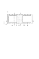
初めに、半導体基板2の表面に素子分離用絶縁膜3を埋め込むことにより、図3及び図4(a)〜(c)に示すように、第1及び第2の活性領域1A,1Bを区画する。具体的には、半導体基板2の主面のうち第1及び第2の活性領域1A,1Bを形成する領域以外の領域に、フォトリソグラフィ法およびドライエッチング法を用いて、深さが例えば250nmのトレンチを形成する。そして、このトレンチの内部を埋める膜厚で、CVD法により、全面にシリコン酸化膜を成膜する。その後、CMP(Chemical Mechanical Polishing)法を用いて全面を平坦化することによりトレンチの内部だけにシリコン酸化膜を残すことにより、第1及び第2の活性領域1A,1Bをを区画する素子分離用絶縁膜3(素子分離領域)を形成する。図3及び図4(a)(b)に示すように、第1の活性領域1Aと第2の活性領域1Bの間に位置する素子分離用絶縁膜3は、上述した素子分離用絶縁膜3aとなる。
First, by embedding an element
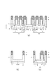
次に、図5及び図6(a)〜(c)に示すように、トレンチT及び各ピラーを形成する。具体的には、まずCVD法を用いて、全面に2nm厚のシリコン酸化膜を形成する。このシリコン酸化膜は、パッド絶縁膜4となる。次に、再度CVD法を用いて、全面に120nm厚のシリコン窒化膜を形成する。このシリコン窒化膜は、マスク膜5となる。続いて、フォトリソグラフィ法により、トレンチTの周囲の素子分離用絶縁膜3(素子分離用絶縁膜3a以外の部分)の上面、及び、各ピラーの形成領域を覆うフォトレジストマスクを形成する。このとき、第1及び第2のダミーピラー7A,7Bの形成領域を覆うフォトレジストマスクのパターンは、素子分離用絶縁膜3aと各活性領域との境界に設ける。そして、このフォトレジストマスクをマスクとする異方性ドライエッチングにより、マスク膜5及びパッド絶縁膜4をエッチングする。これにより、フォトレジストマスクのパターンがマスク膜5及びパッド絶縁膜4に転写される。続いて、フォトレジストマスクを除去した後、マスク膜5をマスクとする異方性ドライエッチングにより、半導体基板2及び素子分離用絶縁膜3aをエッチングする。このエッチングは、トレンチTの深さが150nmとなる程度まで行うようにすることが好ましい。以上により、トレンチT及び各ピラーが形成される。こうして形成された第1及び第2のダミーピラー7A,7Bはそれぞれ、上述したように、半導体ピラー7a及び絶縁体ピラー7bが合体した構造を有する複合ピラーとなる。
Next, as shown in FIG. 5 and FIGS. 6A to 6C, the trench T and each pillar are formed. Specifically, first, a 2 nm thick silicon oxide film is formed on the entire surface by CVD. This silicon oxide film becomes the
次に、図7及び図8(a)〜(c)に示すように、各ピラーの周囲にゲート電極11を形成するとともに、トレンチTの底面のうち第1及び第2の活性領域1A,1Bの内側に相当する領域に下部不純物拡散層9を形成する。具体的には、まず初めに熱酸化法により、半導体基板2の露出面(トレンチTの底面のうち第1及び第2の活性領域1A,1Bの内側に相当する領域、及び各ピラーの側面)に、1nm厚のシリコン酸化膜(不図示)を形成する。続いて、CVD法を用いて4nm厚のシリコン窒化膜を成膜し、全面エッチバックを行うことにより、各ピラーの側面をサイドウォール形状のシリコン窒化膜(不図示)で覆う。次に、再度熱酸化を行うことにより、トレンチTの底面のうち第1及び第2の活性領域1A,1Bの内側に相当する領域に、30nm厚の底絶縁膜8を形成する。このとき、各ピラーの側面はシリコン窒化膜で覆われているので、酸化されない。次いでイオン注入法により、底絶縁膜8の下方の半導体基板2の表面に、n型不純物を導入する。これにより、下部不純物拡散層9が形成される。なお、n型不純物の注入は、平面的に見て各ピラーと重なる部分を除く各活性領域の全面に対して行われる。その結果、下部不純物拡散層9は、上述した各活性領域内の2つの縦型MOSトランジスタに共通となる。注入するn型不純物としては、例えばヒ素や燐を用いることが好適である。
Next, as shown in FIGS. 7 and 8A to 8C, the
下部不純物拡散層9を形成した後には、ドライエッチング法あるいはウェットエッチング法によって、各ピラーの側面に形成したシリコン窒化膜及びシリコン酸化膜を除去する。こうして第1の半導体ピラー6A1,6A2、第2の半導体ピラー6B1,6B2、及び、第1及び第2のダミーピラー7A,7Bのそれぞれを構成する半導体ピラー6aの側面に半導体基板2が露出したら、再度熱酸化を行うことにより、各側面に3nm厚のシリコン酸化膜であるゲート絶縁膜10を形成する。続いてCVD法によって全面に、横方向の膜厚が20nmであるn型不純物含有多結晶シリコン膜を成膜する。そして全面エッチバックを行うことにより、各ピラーの側面にサイドウォール形状のゲート電極11を形成する。こうして各ピラーの側面に形成されたゲート電極11は、図7に示すように、活性領域ごとに一体化して1つのゲート電極11を構成する。これは、上述したように、各ピラーの間隔を、ゲート電極11の横方向の膜厚20nmの2倍以下に設定することによって実現される。
After the lower
なお、上記の工程では、トレンチTの内壁(素子分離用絶縁膜3aを除く素子分離用絶縁膜3の露出面)にもサイドウォール形状のn型不純物含有多結晶シリコン膜が形成されるが、これはゲート電極11として機能するものではないので、図示を省略している。各ピラーの配置は、このn型不純物含有多結晶シリコン膜と各ピラーの側面に形成されるゲート電極11とが一体化しないように設定される。
In the above process, the sidewall-shaped n-type impurity-containing polycrystalline silicon film is also formed on the inner wall of the trench T (exposed surface of the element
ゲート電極11の形成が完了したら、CVD法によって全面にシリコン酸化膜を成膜し、CMP法によって、マスク膜5の上面が露出する程度まで成膜したシリコン酸化膜の表面を平坦化する。これにより、図9及び図10(a)〜(c)に示すように、トレンチTが埋設絶縁膜12によって埋められる。続いて、CVD法によって全面に50nm厚のシリコン酸化膜であるマスク膜13を成膜し、フォトリソグラフィ法とエッチング法を用いて、マスク膜13に開口部O1を設ける。開口部O1の形成位置は、第1の半導体ピラー6A1,6A2及び第2の半導体ピラー6B1,6B2それぞれの上面に形成されたマスク膜5の上面を露出する位置とする。その他の領域に形成されたマスク膜5については、マスク膜13で覆われた状態を維持する。次に、ウェットエッチングによってシリコン窒化膜を選択的に除去することにより、露出したマスク膜5を選択的に除去し、さらにマスク膜5の除去によって露出したパッド絶縁膜4も除去する。これにより、図9及び図10(a)(c)に示すように、第1の半導体ピラー6A1,6A2及び第2の半導体ピラー6B1,6B2それぞれの上側に開口部O2が形成される。開口部O2の底面には半導体基板2の表面が露出し、側面にはゲート電極11及び埋設絶縁膜12が露出する。
When the formation of the
続いて、熱酸化法などによって開口部O2の底面及び内側面にシリコン酸化膜である絶縁膜17を形成した後、イオン注入を行うことにより、図11及び図12(a)〜(c)に示すように、第1の半導体ピラー6A1,6A2及び第2の半導体ピラー6B1,6B2それぞれの上端に上部不純物拡散層16を形成する。次いで、CVD法によって開口部O2の内面を覆う10nm厚のシリコン窒化膜を成膜し、エッチバックを行うことにより、サイドウォール膜18を形成する。このとき、絶縁膜17のうち開口部O2の底面(第1の半導体ピラー6A1,6A2及び第2の半導体ピラー6B1,6B2それぞれの上面)に形成されていた部分も除去し、対応する半導体ピラーの上面を露出させる。絶縁膜17は、サイドウォール膜18の下方と開口部O2内のゲート電極11の露出面に残留することになる。絶縁膜17及びサイドウォール膜18は、ゲート電極11とこの後に形成するシリコンプラグ19との間の絶縁を確保する役割を果たす。
Subsequently, an insulating
次に、選択エピタキシャル成長法を用い、開口部O2を埋設する膜厚で、半導体ピラー51,52の上面にシリコンを成長させる。そして、このシリコンにヒ素などをイオン注入することにより、n型の導電体であるシリコンプラグ19を形成する。シリコンプラグ19は、対応する半導体ピラーの上端に形成されている上部不純物拡散層16と電気的に接触することになる。
Next, silicon is grown on the upper surfaces of the
続いてCVD法により、開口部O1を埋める膜厚でシリコン酸化膜を成膜し、CMP法によって表面を平坦化する。こうして、図13及び図14(a)〜(c)に示すように、全面に層間絶縁膜20が形成される。層間絶縁膜20は、ここで成膜したシリコン酸化膜と、ここまでに成膜したマスク膜13(シリコン酸化膜)とによって構成される。
Subsequently, a silicon oxide film is formed by a CVD method so as to fill the opening O1, and the surface is flattened by the CMP method. Thus, as shown in FIGS. 13 and 14A to 14C, the
層間絶縁膜20を形成したら、次に、フォトリソグラフィ法およびドライエッチング法を用いて、層間絶縁膜20にゲート給電コンタクト孔O3を形成する。ゲート給電コンタクト孔O3は、平面的には、図13に示すように、第1及び第2のダミーピラー7A,7Bをつなぐ長方形の形状を有している。ゲート給電コンタクト孔O3を形成する際のエッチングでは、層間絶縁膜20の下にある埋設絶縁膜12も、ゲート電極11の上端が露出する程度までエッチングする。このようなエッチングを行うことにより、長方形であるゲート給電コンタクト孔O3の両端(長辺方向の両端)には、ダミーピラー6の上方に形成されたマスク膜5の一部と、ダミーピラー6の側面に形成されたゲート電極11の一部とが露出する。一方、ゲート給電コンタクト孔O3の中央部(長辺方向の中央部)には、埋設絶縁膜12が露出する。
After the
その後、CVD法によってチタン(Ti)膜、窒化チタン(TiN)膜、タングステン(W)を順次成膜することにより、ゲート給電コンタクト孔O3を埋める金属膜を成膜し、CMP法によって層間絶縁膜20の表面が露出する程度まで金属膜の表面を平坦化する。これにより、図1(a)(b)及び図2(a)〜(c)に示したように、ゲート給電コンタクト孔O3内に、下面の一端で第1の活性領域1A内のゲート電極11の上端と接し、下面の他端で第2の活性領域1B内のゲート電極11の上端と接する給電コンタクトプラグ41が形成される。
Thereafter, a titanium (Ti) film, a titanium nitride (TiN) film, and tungsten (W) are sequentially formed by a CVD method to form a metal film that fills the gate feeding contact hole O3, and an interlayer insulating film is formed by a CMP method. The surface of the metal film is planarized until the surface of 20 is exposed. As a result, as shown in FIGS. 1A and 1B and FIGS. 2A to 2C, the
上述したように、チタン膜とシリコン膜であるゲート電極11との間にはチタンシリサイド膜が形成され、これにより、ゲート電極11と給電コンタクトプラグ41の接触抵抗が低減される。なお、CVD法によってチタン膜を成膜する場合には、成膜中にシリサイド反応が生ずるので特にシリサイド化のための処理を行う必要はない。一方、上述したように、チタン膜に代えてコバルト(Co)膜やニッケル(Ni)膜など他のシリサイド形成金属を用いる場合には、CVD法ではなくスパッタ法によりこれらの膜を成膜することになるので、成膜中のシリサイド反応が生じず、成膜後に熱処理工程を付加してシリサイド化する必要がある。この場合には、熱処理工程の後、ゲート電極11の表面以外に形成され、未反応状態のCo膜やNi膜を除去する必要もある。窒化チタン膜及びタングステンの成膜はその後に行う。チタン膜であってもスパッタ法で成膜する場合には、同様の処理が必要となる。
As described above, a titanium silicide film is formed between the titanium film and the
次に、CVD法によって、全面にシリコン酸化膜である層間絶縁膜24を成膜する。続いて、フォトリソグラフィ法およびドライエッチング法を用いて、上述したコンタクトプラグ30,31,35を埋め込むためのコンタクト孔を形成し、その内部にチタン膜、窒化チタン膜、タングステン膜を順次成膜することにより、これらの積層膜によって構成されたコンタクトプラグ30,31,35を形成する。そして、CMP法によって層間絶縁膜24の上面に形成された金属膜を除去し、配線33A,33B,34A,34B,42を含む配線層を形成することにより、半導体装置1が完成する。なお、配線層は、スパッタ法により窒化タングステン(WN)膜およびタングステン(W)膜で構成された金属膜を全面に成膜し、その後、フォトリソグラフィとドライエッチング法によりこの金属膜をパターニングすることにより形成することが好適である。
Next, an
以上説明したように、本実施の形態による半導体装置1の製造方法によれば、第1の活性領域1A内のゲート電極11と、第2の活性領域1B内のゲート電極11とを分離する埋設絶縁膜12の上面に形成され、かつ、各ゲート電極11の上端と直接接触する金属膜である給電コンタクトプラグ41を形成することが可能になる。したがって、素子分離領域にもダミーピラーを設けることによりサイドウォール状のシリコン膜で接続する方法や、それぞれのゲート電極をゲートコンタクトプラグによって上層配線に引き出して上層配線で接続する方法に比べて、各活性領域に形成されたゲート電極11の間の配線抵抗を小さくすることが可能になる。
As described above, according to the method of manufacturing the
また、本実施の形態による半導体装置1の製造方法によれば、図5及び図6(a)〜(c)に示した工程で形成する半導体ピラーの数を適宜制御することにより、1つの活性領域内に配置するMOSトランジスタの数を自由に制御することができる。したがって、必要に応じた実効チャネル断面積を確保することが可能になる。
Further, according to the method for manufacturing the
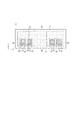
次に、図15(a)(b)及び図16(a)〜(c)を参照しながら、本発明の第2の実施の形態による半導体装置1の構造について説明する。本実施の形態による半導体装置1は、配線33B,34A,34B,42それぞれの形状及び配置の点で、第1の実施の形態による半導体装置1と相違している。また、この相違に伴い、給電コンタクトプラグ41及びコンタクトプラグ31の形状及び配置も相違している。なお、本実施の形態によるコンタクトプラグ31は、第1の活性領域1Aに関してはコンタクトプラグ31Aa,31Abにより構成され、第2の活性領域1Bに関してはコンタクトプラグ31Ba,31Bbにより構成される。さらに、コンタクトプラグ35の位置が相違している。以下では、これらの相違点を中心に説明する。
Next, the structure of the
なお、以下の説明では、各構成の端部等にマイナス側又はプラス側の呼称を付加する場合がある。Y方向のマイナス側端部は図15(a)における下側の端部を示し、Y方向のプラス側端部は図15(a)における上側の端部を示す。また、X方向のマイナス側端部は図15(a)における左側の端部を示し、X方向のプラス側端部は図15(a)における右側の端部を示す。このような呼称を用いると、例えば第1−1の半導体ピラー6A1は、第1−2の半導体ピラー6A2に比べて第1の活性領域1AのX方向のプラス側端部寄りに設けられていると言える。また、第1の活性領域1A内の2つのコンタクトプラグ30はいずれも、同じ第1の活性領域1A内のコンタクトプラグ31Aaに比べて、第1の活性領域1AのY方向のマイナス側端部寄りに設けられていると言える。
In the following description, a negative side or a positive side may be added to the end of each component. The minus side end in the Y direction indicates the lower end in FIG. 15A, and the plus end in the Y direction indicates the upper end in FIG. Further, the minus side end portion in the X direction indicates the left end portion in FIG. 15A, and the plus side end portion in the X direction indicates the right end portion in FIG. When such a designation is used, for example, the first-first semiconductor pillar 6A1 is provided closer to the positive side end in the X direction of the first
まず配線42について、第1の実施の形態では第1及び第2の活性領域1A,1Bの間の領域をY方向に延設されていた(図1(a)参照)が、本実施の形態では、一端が素子分離用絶縁膜3aの上方の領域(第1及び第2の活性領域1A,1Bの間の領域)からそのマイナス側端部側に少し外れた位置にあり、そこから第1の活性領域1AのY方向マイナス側縁辺に沿ってX方向に延設されている。これに伴い、給電コンタクトプラグ41が、各活性領域に対応するダミーピラー6の間から、第1及び第2の活性領域1A,1Bの間の領域と重ならない領域(配線42の一端の下方の位置)までY方向に延設されている(Y方向に拡幅されている)。なお、図15(a)では、給電コンタクトプラグ41のY方向プラス側端部はダミーピラー6のY方向プラス側端部まで至っていないが、これを超えて給電コンタクトプラグ41を延設してもよい。コンタクトプラグ35は、平面的に見て第1及び第2の活性領域1A,1Bの間の領域と重ならない位置に配置され、上面で配線42の一端と電気的に接触し、下面で給電コンタクトプラグ41と電気的に接触する。配線42は、これらコンタクトプラグ35及び給電コンタクトプラグ41を介して、第1の実施の形態と同様、第1及び第2の活性領域1A,1Bそれぞれに対応するゲート電極11と短絡している。
First, regarding the
次に配線34Aについて、第1の実施の形態では第1の活性領域1AのX方向中央付近から、半導体装置1のX方向マイナス側端部に向かってX方向に延設されていた(図1(a)参照)が、本実施の形態では、一端が素子分離用絶縁膜3aの上方の領域(第1及び第2の活性領域1A,1Bの間の領域)のうち、給電コンタクトプラグ41より素子分離用絶縁膜3aのY方向プラス側端部寄りの位置にあり、そこからまず第2の活性領域1Bに向かってX方向に延伸し、一部が第2の活性領域1BにかかったところでY方向に折れ曲がり、そこからさらに半導体装置1のY方向マイナス側端部に向かってY方向に延伸するよう延設されている。これに伴い、まずコンタクトプラグ31Abは、層間絶縁膜24のうち素子分離用絶縁膜3aの上方の領域に位置する部分を貫通しており、上面で配線34Aの一端に接している。一方、コンタクトプラグ31Aaは、垂直方向には層間絶縁膜24、埋設絶縁膜12、及び底絶縁膜8を貫通しており、平面方向には第1の活性領域1Aから第1及び第2の活性領域1A,1Bの間の領域までX方向に延設されている。これにより、コンタクトプラグ31Aaの上面は、素子分離用絶縁膜3aの上方でコンタクトプラグ31Abの下面と接触し、下面は、第1の活性領域1A内で下部不純物拡散層9と接触している。したがって、配線34Aは、コンタクトプラグ31Aa,31Abを介して、第1の実施の形態と同様、第1の活性領域1A内の下部不純物拡散層9と短絡している。
Next, in the first embodiment, the
次に配線34Bについて、第1の実施の形態では第2の活性領域1BのX方向中央付近から、半導体装置1のX方向プラス側端部に向かってX方向に延設されていた(図1(a)参照)が、本実施の形態では、全体的にX方向プラス側及びY方向プラス側にずらして設けられている。その結果、平面的に見て第2の活性領域1Bと重なる部分は一端の一部分のみとなっており、図15(a)に示すように、コンタクトプラグ31(コンタクトプラグ31Ba,31Bb)をY方向に延長する必要が生じている。具体的に説明すると、まずコンタクトプラグ31Bbは、垂直方向には層間絶縁膜24を貫通しており、平面方向には素子分離用絶縁膜3のうち第2の活性領域1BのY方向プラス側縁辺に接する部分に設けられて、上面で配線34Bの一端に接している。一方、コンタクトプラグ31Baは、垂直方向には層間絶縁膜24、埋設絶縁膜12、及び底絶縁膜8を貫通しており、平面方向にはコンタクトプラグ31Bbの下方から第2の活性領域1Bの内側に向かってY方向に延設されている。これにより、コンタクトプラグ31Baの上面は、素子分離用絶縁膜3の上方でコンタクトプラグ31Bbの下面と接触し、下面は、第2の活性領域1B内で下部不純物拡散層9と接触している。したがって、配線34Bは、コンタクトプラグ31Ba,31Bbを介して、第1の実施の形態と同様、第2の活性領域1B内の下部不純物拡散層9と短絡している。
Next, the
次に配線33Bについて、第1の実施の形態では第2の活性領域1BのX方向中央付近から、半導体装置1のX方向プラス側端部に向かってX方向に延設されていた(図1(a)参照)が、本実施の形態では、第2−2の半導体ピラー6B2の位置でY方向に折れ曲がり、そこから半導体装置1のY方向マイナス側端部に向かってY方向に延設されている。配線33Bにかかる第1の実施の形態との相違点は以上の点のみであり、コンタクトプラグ30の位置は第1の実施の形態と同様である。
Next, in the first embodiment, the
以上例示したように、本発明によれば、給電コンタクトプラグ41及びコンタクトプラグ31の形状を変更することにより、配線34A,34B,42のレイアウトを自由に変更することが可能になる。したがって、配線層のレイアウト設計の自由度を向上することが可能になる。
As illustrated above, according to the present invention, the layout of the wirings 34A, 34B, and 42 can be freely changed by changing the shapes of the power
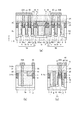
次に、図17(a)(b)及び図18(a)〜(c)を参照しながら、本発明の第3の実施の形態による半導体装置1の構造について説明する。本実施の形態による半導体装置1は、第1−1の半導体ピラー6A1をチャネル領域とするトランジスタと、第1−2の半導体ピラー6A2をチャネル領域とするトランジスタとを、並列ではなく直列に接続する点で、第1の実施の形態による半導体装置1と相違する。それぞれ第2の半導体ピラー6B1,6B2をチャネル領域とする2つのトランジスタについても同様である。また、これに伴ってコンタクトプラグ31が不要になっており、したがって第1及び第2の活性領域1A,1Bにコンタクトプラグ31の設置領域を確保する必要がないので、その分第1及び第2の活性領域1A,1BのY方向の幅が狭められている。また、配線34A,34Bが削除される一方、配線33Aが配線33Aa,33Abの2本に分割され、配線33Bが配線33Ba,33Bbの2本に分割されている。以下では、これらの相違点を中心に説明する。
Next, the structure of the
第1及び第2の活性領域1A,1Bのそれぞれに2本ずつ設置されるトランジスタ自体の構造は、第1の実施の形態と同様である。図18(a)を参照しながら第1の活性領域1Aを例に取って説明すると、まず第1−1の半導体ピラー6A1をチャネル領域とするトランジスタは、第1−1の半導体ピラー6A1の上部不純物拡散層161をソース/ドレインの一方とし、下部不純物拡散層9をソース/ドレインの他方として構成される。一方、第1−2の半導体ピラー6A2をチャネル領域とするトランジスタは、第1−2の半導体ピラー6A2の上部不純物拡散層162をソース/ドレインの一方とし、下部不純物拡散層9をソース/ドレインの他方として構成される。配線34Aaは、コンタクトプラグ30(第1のコンタクトプラグ)を通じて上部不純物拡散層161に接続され、配線34Abは、別のコンタクトプラグ30(第2のコンタクトプラグ)を通じて上部不純物拡散層162に接続される。下部不純物拡散層9は2つのトランジスタに共通である。以上の構成により、これら2つのトランジスタは、配線34Aaと配線34Abとの間に直列に接続されていると言える。第2の活性領域1Bについても同様である。
The structure of two transistors installed in each of the first and second
以上説明したように、本実施の形態による半導体装置1によれば、各活性領域内の2つのトランジスタを直列に接続して用いることができる。したがって、実効チャネル長が長く、高耐圧のトランジスタを得ることが可能になる。
As described above, according to the
なお、本実施の形態で説明した第1及び第2の活性領域1A,1Bのような構造を有する活性領域を追加することにより、直列に接続するトランジスタの数を増やすことが可能である。この場合、活性領域間の接続は、配線33Aa,33Abのような上層配線によって行えばよい。
Note that the number of transistors connected in series can be increased by adding an active region having a structure such as the first and second
また、各上層配線に接続するトランジスタは1つだけでなくてもよい。例えば配線33Aaに複数のトランジスタを接続するには、第1の活性領域1A内に複数の第1の半導体ピラー6A1を設け、それぞれの上部不純物拡散層161を配線34Aaに接続すればよい。
Further, the number of transistors connected to each upper layer wiring is not limited to one. For example, to connect a plurality of transistors to the wiring 33Aa is provided with a
次に、図19(a)(b)、図20(a)〜(c)、及び図21を参照しながら、本発明の第4の実施の形態による半導体装置1の構造について説明する。本実施の形態による半導体装置1は、第2の活性領域1BがNウェル70内に設けられている点、第2の活性領域1B内の上部不純物拡散層161,162及び下部不純物拡散層9が、それぞれp型半導体である上部不純物拡散層711,712及び下部不純物拡散層72に置き換えられている点、第2の活性領域1Bに対応するゲート電極11が、p型不純物含有シリコン膜であるゲート電極73に置き換えられている点、及び、第1の活性領域1A内の上部不純物拡散層161と、第2の活性領域1B内の上部不純物拡散層711とが上層の配線33ABで相互に接続され、配線33Ab,33Bbが設けられない点で、第3の実施の形態による半導体装置1と相違する。以下では、これらの相違点を中心に説明する。
Next, the structure of the
初めに、Nウェル70、p型半導体である上部不純物拡散層711,712及び下部不純物拡散層72、p型不純物含有シリコン膜であるゲート電極73それぞれの、好適な形成方法を説明する。
First, the respective N-well 70, p-type semiconductor upper impurity diffusion layer 71 1 is, 71 2 and the
まず、Nウェル70については、図3に示した状態(素子分離用絶縁膜3を形成し、第1及び第2の活性領域1A,1Bを区画した状態)で第2の活性領域1Bの位置に開口部を有するマスク膜(不図示)を形成し、この開口部を介して半導体基板2内に、イオン注入法を用いて砒素や燐などのn型不純物を導入することにより形成することが好適である。これにより、第2の活性領域1Bに相当する領域にNウェル70が形成され、第2の活性領域1Bがn型(第2の導電型)の活性領域となる。なお、第1の活性領域1Aは、p型(第1の導電型)の活性領域である。
First, for the N well 70, the position of the second
p型半導体である上部不純物拡散層711,712及び下部不純物拡散層72は、半導体基板2にp型不純物となるボロンをイオン注入することにより形成することが好適である。また、p型不純物含有シリコン膜であるゲート電極73は、成膜時にボロンを含有させるCVD法によって形成することができる。具体的には、CVD法での成膜に用いる原料ガスとしてモノシラン(SiH4)とジボラン(B2H6)を同時に供給することで、成膜時にボロンを含有させることが可能になる。この場合、第1活性領域1Aに形成されるn型ゲート電極11と第2活性領域1Bに形成されるp型ゲート電極73は別々の工程で形成される。不純物含有シリコン膜を形成するCVD法に代えて、気相拡散法を用いて不純物を含有させても良い。すなわち、ノンドープシリコン膜のゲート電極材料を形成した後、第2活性領域1Bに形成されたゲート電極材料をマスク膜で覆い、ホスフィン(PH3)雰囲気で熱処理することにより第1活性領域1Aに形成されたゲート電極材にリンを気相拡散させてn型シリコンからなるゲート電極11を形成する。その後マスク膜を除去し、ゲート電極11を新たなマスク膜で覆い、ジボラン(B2H6)雰囲気で熱処理することにより第2活性領域1Bに形成されたゲート電極材にボロンを気相拡散させてp型シリコンからなるゲート電極73を形成する。
p-type semiconductor upper impurity diffusion layer 71 1 is, 71 2 and the lower
このように第2の活性領域1BをNウェル70内に設け、さらに、上部不純物拡散層711,712、下部不純物拡散層72、ゲート電極73をいずれもp型としたことにより、第2の活性領域1Bに形成される2つのトランジスタは、ともにPチャンネル型MOSトランジスタとなる。なお、第1の活性領域1Aに形成される2つのトランジスタは、ともにNチャンネル型MOSトランジスタである。
As described above, the second
本実施の形態による半導体装置1に含まれる4つのトランジスタは、図21に示すように、C−MOS(相補型MOS)インバータ回路を構成する。なお、図21に示すPチャンネル型MOSトランジスタP1,P2はそれぞれ第2の半導体ピラー6B1,6B2をチャネルとするトランジスタであり、Nチャンネル型MOSトランジスタN1,N2はそれぞれ第1の半導体ピラー6A1,6A2をチャネルとするトランジスタである。C−MOSインバータ回路の入力は配線42(第4の配線)、出力は配線33AB(第1の配線)となる。また、配線33Bb(第3の配線)は高位側電源電圧VDDが供給される電源端子を構成し、配線33Ab(第2の配線)は接地電位が供給される接地端子を構成する。
As shown in FIG. 21, the four transistors included in the
以上説明したように、本実施の形態による半導体装置1によれば、第2の活性領域1BをNウェル70内に設け、第2の活性領域1B内の上部不純物拡散層161,162及び下部不純物拡散層9をそれぞれp型半導体である上部不純物拡散層711,712及び下部不純物拡散層72に置き換えたことにより、C−MOSインバータ回路を構成することが可能になっている。これを基本構成とし、基本構成を複数段にわたって接続すれば、複雑なロジック回路を構成することも可能になる。
As described above, according to the
なお、本実施の形態ではトランジスタP2,P1及びトランジスタN1,N2をそれぞれ直列に接続した例を説明したが、第1の実施の形態で説明した構成のように、トランジスタP2,P1及びトランジスタN1,N2をそれぞれ並列に接続してもよい。 In this embodiment, the example in which the transistors P2 and P1 and the transistors N1 and N2 are connected in series has been described. However, as in the configuration described in the first embodiment, the transistors P2 and P1 and the transistors N1 and N1 are connected. N2 may be connected in parallel.
以上、本発明の好ましい実施形態について説明したが、本発明は、上記の実施形態に限定されることなく、本発明の主旨を逸脱しない範囲で種々の変更が可能であり、それらも本発明の範囲内に包含されるものであることはいうまでもない。 The preferred embodiments of the present invention have been described above, but the present invention is not limited to the above-described embodiments, and various modifications can be made without departing from the spirit of the present invention. Needless to say, it is included in the range.
1 半導体装置
1A,1B 活性領域
2 半導体基板
3,3a 素子分離用絶縁膜
4 パッド絶縁膜
5 マスク膜
6A1,6A2,6B1,6B2,7a 半導体ピラー
7A,7B ダミーピラー
7b 絶縁体ピラー
8 底絶縁膜
9,72 下部不純物拡散層
10 ゲート絶縁膜
11,73 ゲート電極
12 埋設絶縁膜
13 マスク膜
16,161,162,711,712 上部不純物拡散層
17 絶縁膜
18 サイドウォール膜
19 シリコンプラグ
20,24 層間絶縁膜
30,31,31Aa,31Ab,31Ba,31Bb,35 コンタクトプラグ
33A,33Aa,33Ab,33AB,33B,33Ba,33Bb,34A,34B,42 配線
41 給電コンタクトプラグ
41 金属膜
70 Nウェル
N1,N2 Nチャンネル型MOSトランジスタ
O1,O2 開口部
O3 ゲート給電コンタクト孔
P1,P2 Nチャンネル型MOSトランジスタ
T トレンチ
1
Claims (14)
前記第1の活性領域に立設された第1の半導体ピラーと、
前記第2の活性領域に立設された第2の半導体ピラーと、
ゲート絶縁膜を介して前記第1の半導体ピラーの側面を覆う第1のゲート電極と、
ゲート絶縁膜を介して前記第2の半導体ピラーの側面を覆う第2のゲート電極と、
前記第1の半導体ピラーの上端に設けられた第1の上部不純物拡散層と、
前記第2の半導体ピラーの上端に設けられた第2の上部不純物拡散層と、
前記第1の半導体ピラーの下部に接して設けられた第1の下部不純物拡散層と、
前記第2の半導体ピラーの下部に接して設けられた第2の下部不純物拡散層と、
前記主面のうち前記第1及び第2の活性領域の間に配置されて前記第1のゲート電極と前記第2のゲート電極とを分離する一方、前記第1及び第2のゲート電極それぞれの上端が上面から突出する膜厚で形成された埋設絶縁膜と、
前記埋設絶縁膜の上面に形成され、下面の一端で前記第1のゲート電極の上端と接触し、下面の他端で前記第2のゲート電極の上端と接触する金属膜と
を備えることを特徴とする半導体装置。 A semiconductor substrate having first and second active regions defined on a main surface;
A first semiconductor pillar erected in the first active region;
A second semiconductor pillar erected in the second active region;
A first gate electrode covering a side surface of the first semiconductor pillar via a gate insulating film;
A second gate electrode covering a side surface of the second semiconductor pillar via a gate insulating film;
A first upper impurity diffusion layer provided at an upper end of the first semiconductor pillar;
A second upper impurity diffusion layer provided at an upper end of the second semiconductor pillar;
A first lower impurity diffusion layer provided in contact with a lower portion of the first semiconductor pillar;
A second lower impurity diffusion layer provided in contact with a lower portion of the second semiconductor pillar;
The first gate electrode is disposed between the first active region and the second active region of the main surface to separate the first gate electrode from the second gate electrode, and each of the first and second gate electrodes. A buried insulating film formed with a film thickness whose upper end protrudes from the upper surface;
A metal film formed on the upper surface of the buried insulating film, in contact with the upper end of the first gate electrode at one end of the lower surface, and in contact with the upper end of the second gate electrode at the other end of the lower surface. A semiconductor device.
前記第1のゲート電極は、前記ゲート絶縁膜を介して前記第1のダミーピラーの側面を覆うよう構成され、
前記第2のゲート電極は、前記ゲート絶縁膜を介して前記第2のダミーピラーの側面を覆うよう構成され、
前記金属膜は、下面の一端で前記第1のゲート電極のうち前記第1のダミーピラーの側面を覆う部分の上端と接触し、下面の他端で前記第2のゲート電極のうち前記第2のダミーピラーの側面を覆う部分の上端と接触する
ことを特徴とする請求項1に記載の半導体装置。 Of the main surface, further comprising first and second dummy pillars erected at positions facing each other across the buried insulating film in plan view,
The first gate electrode is configured to cover a side surface of the first dummy pillar through the gate insulating film,
The second gate electrode is configured to cover a side surface of the second dummy pillar via the gate insulating film,
The metal film is in contact with the upper end of a portion of the first gate electrode that covers the side surface of the first dummy pillar at one end of the lower surface, and the second gate electrode of the second gate electrode at the other end of the lower surface. The semiconductor device according to claim 1, wherein the semiconductor device is in contact with an upper end of a portion covering a side surface of the dummy pillar.
それぞれ前記層間絶縁膜の上面に形成された第1乃至第5の配線を含む配線層と、
前記層間絶縁膜を貫通して設けられ、上面で前記第1の配線と電気的に接触するとともに、下面で前記第1の上部不純物拡散層と電気的に接触する第1のコンタクトプラグと、
前記層間絶縁膜を貫通して設けられ、上面で前記第2の配線と電気的に接触するとともに、下面で前記第2の上部不純物拡散層と電気的に接触する第2のコンタクトプラグと、
前記層間絶縁膜を貫通して設けられ、上面で前記第3の配線と電気的に接触するとともに、下面で前記第1の下部不純物拡散層と電気的に接触する第3のコンタクトプラグと、
前記層間絶縁膜を貫通して設けられ、上面で前記第4の配線と電気的に接触するとともに、下面で前記第2の下部不純物拡散層と電気的に接触する第4のコンタクトプラグと、
前記層間絶縁膜を貫通して設けられ、上面で前記第5の配線と電気的に接触するとともに、下面で前記金属膜と電気的に接触する第5のコンタクトプラグと
をさらに備えることを特徴とする請求項1乃至6のいずれか一項に記載の半導体装置。 An interlayer insulating film;
A wiring layer including first to fifth wirings formed on the upper surface of the interlayer insulating film,
A first contact plug provided through the interlayer insulating film, in electrical contact with the first wiring on the upper surface, and in electrical contact with the first upper impurity diffusion layer on the lower surface;
A second contact plug provided through the interlayer insulating film and in electrical contact with the second wiring on the upper surface and in electrical contact with the second upper impurity diffusion layer on the lower surface;
A third contact plug provided through the interlayer insulating film and in electrical contact with the third wiring on the upper surface and in electrical contact with the first lower impurity diffusion layer on the lower surface;
A fourth contact plug provided through the interlayer insulating film, in electrical contact with the fourth wiring on the upper surface, and in electrical contact with the second lower impurity diffusion layer on the lower surface;
A fifth contact plug provided through the interlayer insulating film and in electrical contact with the fifth wiring on the upper surface and in electrical contact with the metal film on the lower surface; The semiconductor device according to claim 1.
それぞれ前記第1の活性領域に立設された複数の第1の半導体ピラーと、
それぞれ前記第2の活性領域に立設された複数の第2の半導体ピラーと、
ゲート絶縁膜を介して前記複数の第1の半導体ピラーの側面を覆う第1のゲート電極と、
ゲート絶縁膜を介して前記複数の第2の半導体ピラーの側面を覆う第2のゲート電極と、
それぞれ前記複数の第1の半導体ピラーの上端に設けられた複数の第1の上部不純物拡散層と、
それぞれ前記複数の第2の半導体ピラーの上端に設けられた複数の第2の上部不純物拡散層と、
前記複数の第1の半導体ピラーそれぞれの下部に接して設けられた第1の下部不純物拡散層と、
前記複数の第2の半導体ピラーそれぞれの下部に接して設けられた第2の下部不純物拡散層と、
前記主面のうち前記第1及び第2の活性領域の間に配置されて前記第1のゲート電極と前記第2のゲート電極とを分離する一方、前記第1及び第2のゲート電極それぞれの上端が上面から突出する膜厚で形成された埋設絶縁膜と、
前記埋設絶縁膜の上面に形成され、下面の一端で前記第1のゲート電極の上端と接触し、下面の他端で前記第2のゲート電極の上端と接触する金属膜と
を備えることを特徴とする半導体装置。 A semiconductor substrate having first and second active regions defined on a main surface;
A plurality of first semiconductor pillars each erected in the first active region;
A plurality of second semiconductor pillars each erected in the second active region;
A first gate electrode covering a side surface of the plurality of first semiconductor pillars via a gate insulating film;
A second gate electrode covering a side surface of the plurality of second semiconductor pillars via a gate insulating film;
A plurality of first upper impurity diffusion layers respectively provided at upper ends of the plurality of first semiconductor pillars;
A plurality of second upper impurity diffusion layers respectively provided at upper ends of the plurality of second semiconductor pillars;
A first lower impurity diffusion layer provided in contact with a lower portion of each of the plurality of first semiconductor pillars;
A second lower impurity diffusion layer provided in contact with a lower portion of each of the plurality of second semiconductor pillars;
The first gate electrode is disposed between the first active region and the second active region of the main surface to separate the first gate electrode from the second gate electrode, and each of the first and second gate electrodes. A buried insulating film formed with a film thickness whose upper end protrudes from the upper surface;
A metal film formed on the upper surface of the buried insulating film, in contact with the upper end of the first gate electrode at one end of the lower surface, and in contact with the upper end of the second gate electrode at the other end of the lower surface. A semiconductor device.
それぞれ前記層間絶縁膜の上面に形成された第1乃至第5の配線を含む配線層と、
それぞれ前記層間絶縁膜を貫通して設けられ、上面で前記第1の配線と電気的に接触するとともに、下面でそれぞれ前記複数の第1の上部不純物拡散層と電気的に接触する複数の第1のコンタクトプラグと、
それぞれ前記層間絶縁膜を貫通して設けられ、上面で前記第2の配線と電気的に接触するとともに、下面でそれぞれ前記複数の第2の上部不純物拡散層と電気的に接触する複数の第2のコンタクトプラグと、
前記層間絶縁膜を貫通して設けられ、上面で前記第3の配線と電気的に接触するとともに、下面で前記第1の下部不純物拡散層と電気的に接触する第3のコンタクトプラグと、
前記層間絶縁膜を貫通して設けられ、上面で前記第4の配線と電気的に接触するとともに、下面で前記第2の下部不純物拡散層と電気的に接触する第4のコンタクトプラグと、
前記層間絶縁膜を貫通して設けられ、上面で前記第5の配線と電気的に接触するとともに、下面で前記金属膜と電気的に接触する第5のコンタクトプラグと
をさらに備えることを特徴とする請求項8に記載の半導体装置。 An interlayer insulating film;
A wiring layer including first to fifth wirings formed on the upper surface of the interlayer insulating film,
Each of the first insulating layers is provided through the interlayer insulating film, and is in electrical contact with the first wiring on the upper surface and is electrically in contact with the plurality of first upper impurity diffusion layers on the lower surface. Contact plugs of
Each of the second insulating layers is provided so as to penetrate through the interlayer insulating film, and is in electrical contact with the second wiring on the upper surface and is electrically in contact with the plurality of second upper impurity diffusion layers on the lower surface. Contact plugs of
A third contact plug provided through the interlayer insulating film and in electrical contact with the third wiring on the upper surface and in electrical contact with the first lower impurity diffusion layer on the lower surface;
A fourth contact plug provided through the interlayer insulating film, in electrical contact with the fourth wiring on the upper surface, and in electrical contact with the second lower impurity diffusion layer on the lower surface;
A fifth contact plug provided through the interlayer insulating film and in electrical contact with the fifth wiring on the upper surface and in electrical contact with the metal film on the lower surface; The semiconductor device according to claim 8.
前記第1のコンタクトプラグは、平面的に見て前記第1及び第2の活性領域の間の領域と重ならない位置で、前記金属膜及び前記第5の配線のそれぞれと電気的に接触する
ことを特徴とする請求項9に記載の半導体装置。 The metal film is extended to a region that does not overlap with a region between the first and second active regions in plan view,
The first contact plug is in electrical contact with each of the metal film and the fifth wiring at a position that does not overlap with a region between the first and second active regions in plan view. The semiconductor device according to claim 9.
それぞれ前記層間絶縁膜の上面に形成された第1乃至第5の配線を含む配線層と、
それぞれ前記層間絶縁膜を貫通して設けられ、上面で前記第1の配線と電気的に接触するとともに、下面でそれぞれ前記複数の第1の上部不純物拡散層のうちの一部と電気的に接触する少なくとも1つの第1のコンタクトプラグと、
それぞれ前記層間絶縁膜を貫通して設けられ、上面で前記第2の配線と電気的に接触するとともに、下面でそれぞれ前記複数の第1の上部不純物拡散層のうちの残りの一部と電気的に接触する少なくとも1つの第2のコンタクトプラグと、
それぞれ前記層間絶縁膜を貫通して設けられ、上面で前記第3の配線と電気的に接触するとともに、下面でそれぞれ前記複数の第2の上部不純物拡散層のうちの一部と電気的に接触する少なくとも1つの第3のコンタクトプラグと、
それぞれ前記層間絶縁膜を貫通して設けられ、上面で前記第4の配線と電気的に接触するとともに、下面でそれぞれ前記複数の第2の上部不純物拡散層のうちの残りの一部と電気的に接触する少なくとも1つの第4のコンタクトプラグと、
前記層間絶縁膜を貫通して設けられ、上面で前記第5の配線と電気的に接触するとともに、下面で前記金属膜と電気的に接触する第5のコンタクトプラグと
をさらに備えることを特徴とする請求項8に記載の半導体装置。 An interlayer insulating film;
A wiring layer including first to fifth wirings formed on the upper surface of the interlayer insulating film,
Each is provided through the interlayer insulating film, and is in electrical contact with the first wiring on the top surface, and is in electrical contact with a part of the plurality of first upper impurity diffusion layers on the bottom surface. At least one first contact plug that
Each is provided through the interlayer insulating film, and is in electrical contact with the second wiring on the upper surface, and electrically connected to the remaining part of the plurality of first upper impurity diffusion layers on the lower surface. At least one second contact plug in contact with
Each is provided through the interlayer insulating film, and is in electrical contact with the third wiring on the upper surface, and is in electrical contact with a part of the plurality of second upper impurity diffusion layers on the lower surface. At least one third contact plug that
Each is provided through the interlayer insulating film, is in electrical contact with the fourth wiring on the upper surface, and is electrically connected to the remaining part of the plurality of second upper impurity diffusion layers on the lower surface. At least one fourth contact plug in contact with
A fifth contact plug provided through the interlayer insulating film and in electrical contact with the fifth wiring on the upper surface and in electrical contact with the metal film on the lower surface; The semiconductor device according to claim 8.
前記第2の活性領域は前記第1の導電型とは異なる第2の導電型であり、
前記第1の配線と前記第3の配線とは互いに接続される
ことを特徴とする請求項11に記載の半導体装置。 The first active region is of a first conductivity type;
The second active region has a second conductivity type different from the first conductivity type;
The semiconductor device according to claim 11, wherein the first wiring and the third wiring are connected to each other.
それぞれ前記第1の活性領域に立設された複数の第1の半導体ピラーと、
それぞれ前記第2の活性領域に立設された複数の第2の半導体ピラーと、
ゲート絶縁膜を介して前記複数の第1の半導体ピラーの側面を覆う第1のゲート電極と、
ゲート絶縁膜を介して前記複数の第2の半導体ピラーの側面を覆う第2のゲート電極と、
それぞれ前記複数の第1の半導体ピラーの上端に設けられた複数の第1の上部不純物拡散層と、
それぞれ前記複数の第2の半導体ピラーの上端に設けられた複数の第2の上部不純物拡散層と、
前記複数の第1の半導体ピラーそれぞれの下部に接して設けられた第1の下部不純物拡散層と、
前記複数の第2の半導体ピラーそれぞれの下部に接して設けられた第2の下部不純物拡散層と、
前記主面のうち前記第1及び第2の活性領域の間に配置されて前記第1のゲート電極と前記第2のゲート電極とを分離する一方、前記第1及び第2のゲート電極それぞれの上端が上面から突出する膜厚で形成された埋設絶縁膜と、
前記埋設絶縁膜の上面に形成され、下面の一端で前記第1のゲート電極の上端と接触し、下面の他端で前記第2のゲート電極の上端と接触する金属膜とを備え、
前記複数の第1の上部不純物拡散層の一部と、前記複数の第2の上部不純物拡散層の一部とは、互いに電気的に接続される
ことを特徴とする半導体装置。 A semiconductor substrate in which a first active region having a first conductivity type and a second active region having a second conductivity type different from the first conductivity type are partitioned on a main surface;
A plurality of first semiconductor pillars each erected in the first active region;
A plurality of second semiconductor pillars each erected in the second active region;
A first gate electrode covering a side surface of the plurality of first semiconductor pillars via a gate insulating film;
A second gate electrode covering a side surface of the plurality of second semiconductor pillars via a gate insulating film;
A plurality of first upper impurity diffusion layers respectively provided at upper ends of the plurality of first semiconductor pillars;
A plurality of second upper impurity diffusion layers respectively provided at upper ends of the plurality of second semiconductor pillars;
A first lower impurity diffusion layer provided in contact with a lower portion of each of the plurality of first semiconductor pillars;
A second lower impurity diffusion layer provided in contact with a lower portion of each of the plurality of second semiconductor pillars;
The first gate electrode is disposed between the first active region and the second active region of the main surface to separate the first gate electrode from the second gate electrode, and each of the first and second gate electrodes. A buried insulating film formed with a film thickness whose upper end protrudes from the upper surface;
A metal film formed on the upper surface of the buried insulating film, in contact with the upper end of the first gate electrode at one end of the lower surface, and in contact with the upper end of the second gate electrode at the other end of the lower surface;
A part of the plurality of first upper impurity diffusion layers and a part of the plurality of second upper impurity diffusion layers are electrically connected to each other.
それぞれ前記層間絶縁膜の上面に形成された第1乃至第4の配線を含む配線層と、
それぞれ前記層間絶縁膜を貫通して設けられ、上面で前記第1の配線と電気的に接触するとともに、下面でそれぞれ前記複数の第1の上部不純物拡散層のうちの前記一部と電気的に接触する少なくとも1つの第1のコンタクトプラグと、
それぞれ前記層間絶縁膜を貫通して設けられ、上面で前記第2の配線と電気的に接触するとともに、下面でそれぞれ前記複数の第1の上部不純物拡散層のうちの残りの一部と電気的に接触する少なくとも1つの第2のコンタクトプラグと、
それぞれ前記層間絶縁膜を貫通して設けられ、上面で前記第1の配線と電気的に接触するとともに、下面でそれぞれ前記複数の第2の上部不純物拡散層のうちの前記一部と電気的に接触する少なくとも1つの第3のコンタクトプラグと、
それぞれ前記層間絶縁膜を貫通して設けられ、上面で前記第3の配線と電気的に接触するとともに、下面でそれぞれ前記複数の第2の上部不純物拡散層のうちの残りの一部と電気的に接触する少なくとも1つの第4のコンタクトプラグと、
前記層間絶縁膜を貫通して設けられ、上面で前記第4の配線と電気的に接触するとともに、下面で前記金属膜と電気的に接触する第5のコンタクトプラグと
をさらに備えることを特徴とする請求項13に記載の半導体装置。 An interlayer insulating film;
A wiring layer including first to fourth wirings formed on the upper surface of the interlayer insulating film,
Each is provided through the interlayer insulating film, is in electrical contact with the first wiring on the upper surface, and is electrically connected to the part of the plurality of first upper impurity diffusion layers on the lower surface. At least one first contact plug in contact;
Each is provided through the interlayer insulating film, and is in electrical contact with the second wiring on the upper surface, and electrically connected to the remaining part of the plurality of first upper impurity diffusion layers on the lower surface. At least one second contact plug in contact with
Each is provided through the interlayer insulating film, and is in electrical contact with the first wiring on the upper surface and electrically with the part of the plurality of second upper impurity diffusion layers on the lower surface. At least one third contact plug in contact;
Each is provided through the interlayer insulating film, and is in electrical contact with the third wiring on the upper surface, and electrically connected to the remaining part of the plurality of second upper impurity diffusion layers on the lower surface, respectively. At least one fourth contact plug in contact with
A fifth contact plug provided through the interlayer insulating film and in electrical contact with the fourth wiring on the upper surface and in electrical contact with the metal film on the lower surface; The semiconductor device according to claim 13.
Priority Applications (1)
| Application Number | Priority Date | Filing Date | Title |
|---|---|---|---|
| JP2013083309A JP2014207295A (en) | 2013-04-11 | 2013-04-11 | Semiconductor device |
Applications Claiming Priority (1)
| Application Number | Priority Date | Filing Date | Title |
|---|---|---|---|
| JP2013083309A JP2014207295A (en) | 2013-04-11 | 2013-04-11 | Semiconductor device |
Publications (1)
| Publication Number | Publication Date |
|---|---|
| JP2014207295A true JP2014207295A (en) | 2014-10-30 |
Family
ID=52120651
Family Applications (1)
| Application Number | Title | Priority Date | Filing Date |
|---|---|---|---|
| JP2013083309A Pending JP2014207295A (en) | 2013-04-11 | 2013-04-11 | Semiconductor device |
Country Status (1)
| Country | Link |
|---|---|
| JP (1) | JP2014207295A (en) |
Cited By (1)
| Publication number | Priority date | Publication date | Assignee | Title |
|---|---|---|---|---|
| US9966376B2 (en) | 2015-10-08 | 2018-05-08 | Samsung Electronics Co., Ltd. | Semiconductor devices and inverter having the same |
-
2013
- 2013-04-11 JP JP2013083309A patent/JP2014207295A/en active Pending
Cited By (1)
| Publication number | Priority date | Publication date | Assignee | Title |
|---|---|---|---|---|
| US9966376B2 (en) | 2015-10-08 | 2018-05-08 | Samsung Electronics Co., Ltd. | Semiconductor devices and inverter having the same |
Similar Documents
| Publication | Publication Date | Title |
|---|---|---|
| CN107359165B (en) | vertical memory device | |
| US9202921B2 (en) | Semiconductor device and method of making the same | |
| KR102496973B1 (en) | Semiconductor devices and methods of manufacturing the same | |
| US9245893B1 (en) | Semiconductor constructions having grooves dividing active regions | |
| US8294205B2 (en) | Semiconductor device and method of forming semiconductor device | |
| US9209192B2 (en) | Semiconductor device and method of fabricating the same | |
| US8928073B2 (en) | Semiconductor devices including guard ring structures | |
| CN107611132B (en) | vertical memory device | |
| KR20180037662A (en) | Semiconductor devices and methods of manufacturing the same | |
| TW201637209A (en) | Semiconductor device | |
| JP2008300623A (en) | Semiconductor device, manufacturing method thereof, and data processing system | |
| JP2012174790A (en) | Semiconductor device and manufacturing method of the same | |
| JP2011023483A (en) | Semiconductor device, manufacturing method thereof, and data processing system | |
| JP2011077185A (en) | Semiconductor device, method of manufacturing semiconductor device, and data processing system | |
| CN101937915B (en) | The manufacture method of semiconductor device and semiconductor device | |
| US8013373B2 (en) | Semiconductor device having MOS-transistor formed on semiconductor substrate and method for manufacturing thereof | |
| WO2014112496A1 (en) | Semiconductor device and method for manufacturing same | |
| JP2011204745A (en) | Semiconductor device and manufacturing method of the same | |
| US8778770B2 (en) | Semiconductor device and method for manufacturing the same | |
| US9570447B2 (en) | Semiconductor device and production method therefor | |
| WO2014181819A1 (en) | Semiconductor device | |
| CN116096081A (en) | Semiconductor device with a semiconductor layer having a plurality of semiconductor layers | |
| JP2011211111A (en) | Nonvolatile semiconductor memory device and method of manufacturing the same | |
| JP2012004510A (en) | Semiconductor device and method of manufacturing the same | |
| WO2014073361A1 (en) | Semiconductor device |