JP2014505367A - 電子部品のプリント基板又はプリント基板中間体への集積方法及びプリント基板又はプリント基板中間体 - Google Patents
電子部品のプリント基板又はプリント基板中間体への集積方法及びプリント基板又はプリント基板中間体 Download PDFInfo
- Publication number
- JP2014505367A JP2014505367A JP2013550705A JP2013550705A JP2014505367A JP 2014505367 A JP2014505367 A JP 2014505367A JP 2013550705 A JP2013550705 A JP 2013550705A JP 2013550705 A JP2013550705 A JP 2013550705A JP 2014505367 A JP2014505367 A JP 2014505367A
- Authority
- JP
- Japan
- Prior art keywords
- printed circuit
- circuit board
- layer
- conductive layer
- electronic component
- Prior art date
- Legal status (The legal status is an assumption and is not a legal conclusion. Google has not performed a legal analysis and makes no representation as to the accuracy of the status listed.)
- Granted
Links
Images




Classifications
-
- H—ELECTRICITY
- H05—ELECTRIC TECHNIQUES NOT OTHERWISE PROVIDED FOR
- H05K—PRINTED CIRCUITS; CASINGS OR CONSTRUCTIONAL DETAILS OF ELECTRIC APPARATUS; MANUFACTURE OF ASSEMBLAGES OF ELECTRICAL COMPONENTS
- H05K1/00—Printed circuits
- H05K1/18—Printed circuits structurally associated with non-printed electric components
- H05K1/182—Printed circuits structurally associated with non-printed electric components associated with components mounted in printed circuit boards [PCB], e.g. insert-mounted components [IMC]
- H05K1/185—Printed circuits structurally associated with non-printed electric components associated with components mounted in printed circuit boards [PCB], e.g. insert-mounted components [IMC] associated with components encapsulated in the insulating substrate of the PCBs; associated with components incorporated in internal layers of multilayer circuit boards
- H05K1/188—Printed circuits structurally associated with non-printed electric components associated with components mounted in printed circuit boards [PCB], e.g. insert-mounted components [IMC] associated with components encapsulated in the insulating substrate of the PCBs; associated with components incorporated in internal layers of multilayer circuit boards manufactured by mounting on or attaching to a structure having a conductive layer, e.g. a metal foil, such that the terminals of the component are connected to or adjacent to the conductive layer before embedding, and by using the conductive layer, which is patterned after embedding, at least partially for connecting the component
-
- B—PERFORMING OPERATIONS; TRANSPORTING
- B60—VEHICLES IN GENERAL
- B60T—VEHICLE BRAKE CONTROL SYSTEMS OR PARTS THEREOF; BRAKE CONTROL SYSTEMS OR PARTS THEREOF, IN GENERAL; ARRANGEMENT OF BRAKING ELEMENTS ON VEHICLES IN GENERAL; PORTABLE DEVICES FOR PREVENTING UNWANTED MOVEMENT OF VEHICLES; VEHICLE MODIFICATIONS TO FACILITATE COOLING OF BRAKES
- B60T5/00—Vehicle modifications to facilitate cooling of brakes
-
- H—ELECTRICITY
- H05—ELECTRIC TECHNIQUES NOT OTHERWISE PROVIDED FOR
- H05K—PRINTED CIRCUITS; CASINGS OR CONSTRUCTIONAL DETAILS OF ELECTRIC APPARATUS; MANUFACTURE OF ASSEMBLAGES OF ELECTRICAL COMPONENTS
- H05K1/00—Printed circuits
- H05K1/02—Details
- H05K1/0201—Thermal arrangements, e.g. for cooling, heating or preventing overheating
- H05K1/0203—Cooling of mounted components
- H05K1/0207—Cooling of mounted components using internal conductor planes parallel to the surface for thermal conduction, e.g. power planes
-
- B—PERFORMING OPERATIONS; TRANSPORTING
- B60—VEHICLES IN GENERAL
- B60T—VEHICLE BRAKE CONTROL SYSTEMS OR PARTS THEREOF; BRAKE CONTROL SYSTEMS OR PARTS THEREOF, IN GENERAL; ARRANGEMENT OF BRAKING ELEMENTS ON VEHICLES IN GENERAL; PORTABLE DEVICES FOR PREVENTING UNWANTED MOVEMENT OF VEHICLES; VEHICLE MODIFICATIONS TO FACILITATE COOLING OF BRAKES
- B60T17/00—Component parts, details, or accessories of power brake systems not covered by groups B60T8/00, B60T13/00 or B60T15/00, or presenting other characteristic features
- B60T17/18—Safety devices; Monitoring
- B60T17/22—Devices for monitoring or checking brake systems; Signal devices
-
- F—MECHANICAL ENGINEERING; LIGHTING; HEATING; WEAPONS; BLASTING
- F16—ENGINEERING ELEMENTS AND UNITS; GENERAL MEASURES FOR PRODUCING AND MAINTAINING EFFECTIVE FUNCTIONING OF MACHINES OR INSTALLATIONS; THERMAL INSULATION IN GENERAL
- F16D—COUPLINGS FOR TRANSMITTING ROTATION; CLUTCHES; BRAKES
- F16D13/00—Friction clutches
- F16D13/58—Details
- F16D13/72—Features relating to cooling
-
- F—MECHANICAL ENGINEERING; LIGHTING; HEATING; WEAPONS; BLASTING
- F16—ENGINEERING ELEMENTS AND UNITS; GENERAL MEASURES FOR PRODUCING AND MAINTAINING EFFECTIVE FUNCTIONING OF MACHINES OR INSTALLATIONS; THERMAL INSULATION IN GENERAL
- F16D—COUPLINGS FOR TRANSMITTING ROTATION; CLUTCHES; BRAKES
- F16D65/00—Parts or details
- F16D65/02—Braking members; Mounting thereof
- F16D65/12—Discs; Drums for disc brakes
- F16D65/128—Discs; Drums for disc brakes characterised by means for cooling
-
- F—MECHANICAL ENGINEERING; LIGHTING; HEATING; WEAPONS; BLASTING
- F16—ENGINEERING ELEMENTS AND UNITS; GENERAL MEASURES FOR PRODUCING AND MAINTAINING EFFECTIVE FUNCTIONING OF MACHINES OR INSTALLATIONS; THERMAL INSULATION IN GENERAL
- F16D—COUPLINGS FOR TRANSMITTING ROTATION; CLUTCHES; BRAKES
- F16D65/00—Parts or details
- F16D65/78—Features relating to cooling
- F16D65/80—Features relating to cooling for externally-engaging brakes
- F16D65/807—Features relating to cooling for externally-engaging brakes with open cooling system, e.g. cooled by air
-
- F—MECHANICAL ENGINEERING; LIGHTING; HEATING; WEAPONS; BLASTING
- F16—ENGINEERING ELEMENTS AND UNITS; GENERAL MEASURES FOR PRODUCING AND MAINTAINING EFFECTIVE FUNCTIONING OF MACHINES OR INSTALLATIONS; THERMAL INSULATION IN GENERAL
- F16D—COUPLINGS FOR TRANSMITTING ROTATION; CLUTCHES; BRAKES
- F16D65/00—Parts or details
- F16D65/78—Features relating to cooling
- F16D65/82—Features relating to cooling for internally-engaging brakes
- F16D65/827—Features relating to cooling for internally-engaging brakes with open cooling system, e.g. cooled by air
-
- F—MECHANICAL ENGINEERING; LIGHTING; HEATING; WEAPONS; BLASTING
- F16—ENGINEERING ELEMENTS AND UNITS; GENERAL MEASURES FOR PRODUCING AND MAINTAINING EFFECTIVE FUNCTIONING OF MACHINES OR INSTALLATIONS; THERMAL INSULATION IN GENERAL
- F16D—COUPLINGS FOR TRANSMITTING ROTATION; CLUTCHES; BRAKES
- F16D65/00—Parts or details
- F16D65/78—Features relating to cooling
- F16D65/84—Features relating to cooling for disc brakes
- F16D65/847—Features relating to cooling for disc brakes with open cooling system, e.g. cooled by air
-
- F—MECHANICAL ENGINEERING; LIGHTING; HEATING; WEAPONS; BLASTING
- F16—ENGINEERING ELEMENTS AND UNITS; GENERAL MEASURES FOR PRODUCING AND MAINTAINING EFFECTIVE FUNCTIONING OF MACHINES OR INSTALLATIONS; THERMAL INSULATION IN GENERAL
- F16D—COUPLINGS FOR TRANSMITTING ROTATION; CLUTCHES; BRAKES
- F16D69/00—Friction linings; Attachment thereof; Selection of coacting friction substances or surfaces
- F16D69/02—Composition of linings ; Methods of manufacturing
- F16D69/025—Compositions based on an organic binder
- F16D69/026—Compositions based on an organic binder containing fibres
-
- H—ELECTRICITY
- H05—ELECTRIC TECHNIQUES NOT OTHERWISE PROVIDED FOR
- H05K—PRINTED CIRCUITS; CASINGS OR CONSTRUCTIONAL DETAILS OF ELECTRIC APPARATUS; MANUFACTURE OF ASSEMBLAGES OF ELECTRICAL COMPONENTS
- H05K1/00—Printed circuits
- H05K1/02—Details
- H05K1/0201—Thermal arrangements, e.g. for cooling, heating or preventing overheating
- H05K1/0212—Printed circuits or mounted components having integral heating means
-
- H—ELECTRICITY
- H05—ELECTRIC TECHNIQUES NOT OTHERWISE PROVIDED FOR
- H05K—PRINTED CIRCUITS; CASINGS OR CONSTRUCTIONAL DETAILS OF ELECTRIC APPARATUS; MANUFACTURE OF ASSEMBLAGES OF ELECTRICAL COMPONENTS
- H05K1/00—Printed circuits
- H05K1/02—Details
- H05K1/0271—Arrangements for reducing stress or warp in rigid printed circuit boards, e.g. caused by loads, vibrations or differences in thermal expansion
-
- H—ELECTRICITY
- H05—ELECTRIC TECHNIQUES NOT OTHERWISE PROVIDED FOR
- H05K—PRINTED CIRCUITS; CASINGS OR CONSTRUCTIONAL DETAILS OF ELECTRIC APPARATUS; MANUFACTURE OF ASSEMBLAGES OF ELECTRICAL COMPONENTS
- H05K1/00—Printed circuits
- H05K1/02—Details
- H05K1/09—Use of materials for the conductive, e.g. metallic pattern
-
- H—ELECTRICITY
- H05—ELECTRIC TECHNIQUES NOT OTHERWISE PROVIDED FOR
- H05K—PRINTED CIRCUITS; CASINGS OR CONSTRUCTIONAL DETAILS OF ELECTRIC APPARATUS; MANUFACTURE OF ASSEMBLAGES OF ELECTRICAL COMPONENTS
- H05K1/00—Printed circuits
- H05K1/18—Printed circuits structurally associated with non-printed electric components
- H05K1/182—Printed circuits structurally associated with non-printed electric components associated with components mounted in printed circuit boards [PCB], e.g. insert-mounted components [IMC]
- H05K1/185—Printed circuits structurally associated with non-printed electric components associated with components mounted in printed circuit boards [PCB], e.g. insert-mounted components [IMC] associated with components encapsulated in the insulating substrate of the PCBs; associated with components incorporated in internal layers of multilayer circuit boards
- H05K1/186—Printed circuits structurally associated with non-printed electric components associated with components mounted in printed circuit boards [PCB], e.g. insert-mounted components [IMC] associated with components encapsulated in the insulating substrate of the PCBs; associated with components incorporated in internal layers of multilayer circuit boards manufactured by mounting on or connecting to patterned circuits before or during embedding
- H05K1/187—Printed circuits structurally associated with non-printed electric components associated with components mounted in printed circuit boards [PCB], e.g. insert-mounted components [IMC] associated with components encapsulated in the insulating substrate of the PCBs; associated with components incorporated in internal layers of multilayer circuit boards manufactured by mounting on or connecting to patterned circuits before or during embedding the patterned circuits being prefabricated circuits, which are not yet attached to a permanent insulating substrate, e.g. on a temporary carrier
-
- H—ELECTRICITY
- H05—ELECTRIC TECHNIQUES NOT OTHERWISE PROVIDED FOR
- H05K—PRINTED CIRCUITS; CASINGS OR CONSTRUCTIONAL DETAILS OF ELECTRIC APPARATUS; MANUFACTURE OF ASSEMBLAGES OF ELECTRICAL COMPONENTS
- H05K3/00—Apparatus or processes for manufacturing printed circuits
- H05K3/30—Assembling printed circuits with electric components, e.g. with resistors
-
- H—ELECTRICITY
- H10—SEMICONDUCTOR DEVICES; ELECTRIC SOLID-STATE DEVICES NOT OTHERWISE PROVIDED FOR
- H10W—GENERIC PACKAGES, INTERCONNECTIONS, CONNECTORS OR OTHER CONSTRUCTIONAL DETAILS OF DEVICES COVERED BY CLASS H10
- H10W70/00—Package substrates; Interposers; Redistribution layers [RDL]
- H10W70/60—Insulating or insulated package substrates; Interposers; Redistribution layers
-
- F—MECHANICAL ENGINEERING; LIGHTING; HEATING; WEAPONS; BLASTING
- F16—ENGINEERING ELEMENTS AND UNITS; GENERAL MEASURES FOR PRODUCING AND MAINTAINING EFFECTIVE FUNCTIONING OF MACHINES OR INSTALLATIONS; THERMAL INSULATION IN GENERAL
- F16D—COUPLINGS FOR TRANSMITTING ROTATION; CLUTCHES; BRAKES
- F16D65/00—Parts or details
- F16D65/78—Features relating to cooling
- F16D2065/783—Features relating to cooling cooling control or adjustment
-
- F—MECHANICAL ENGINEERING; LIGHTING; HEATING; WEAPONS; BLASTING
- F16—ENGINEERING ELEMENTS AND UNITS; GENERAL MEASURES FOR PRODUCING AND MAINTAINING EFFECTIVE FUNCTIONING OF MACHINES OR INSTALLATIONS; THERMAL INSULATION IN GENERAL
- F16D—COUPLINGS FOR TRANSMITTING ROTATION; CLUTCHES; BRAKES
- F16D66/00—Arrangements for monitoring working conditions, e.g. wear, temperature
- F16D2066/001—Temperature
-
- F—MECHANICAL ENGINEERING; LIGHTING; HEATING; WEAPONS; BLASTING
- F16—ENGINEERING ELEMENTS AND UNITS; GENERAL MEASURES FOR PRODUCING AND MAINTAINING EFFECTIVE FUNCTIONING OF MACHINES OR INSTALLATIONS; THERMAL INSULATION IN GENERAL
- F16D—COUPLINGS FOR TRANSMITTING ROTATION; CLUTCHES; BRAKES
- F16D69/00—Friction linings; Attachment thereof; Selection of coacting friction substances or surfaces
- F16D2069/004—Profiled friction surfaces, e.g. grooves, dimples
-
- F—MECHANICAL ENGINEERING; LIGHTING; HEATING; WEAPONS; BLASTING
- F16—ENGINEERING ELEMENTS AND UNITS; GENERAL MEASURES FOR PRODUCING AND MAINTAINING EFFECTIVE FUNCTIONING OF MACHINES OR INSTALLATIONS; THERMAL INSULATION IN GENERAL
- F16D—COUPLINGS FOR TRANSMITTING ROTATION; CLUTCHES; BRAKES
- F16D2200/00—Materials; Production methods therefor
- F16D2200/006—Materials; Production methods therefor containing fibres or particles
- F16D2200/0073—Materials; Production methods therefor containing fibres or particles having lubricating properties
-
- F—MECHANICAL ENGINEERING; LIGHTING; HEATING; WEAPONS; BLASTING
- F16—ENGINEERING ELEMENTS AND UNITS; GENERAL MEASURES FOR PRODUCING AND MAINTAINING EFFECTIVE FUNCTIONING OF MACHINES OR INSTALLATIONS; THERMAL INSULATION IN GENERAL
- F16D—COUPLINGS FOR TRANSMITTING ROTATION; CLUTCHES; BRAKES
- F16D2250/00—Manufacturing; Assembly
- F16D2250/0038—Surface treatment
- F16D2250/0046—Coating
-
- F—MECHANICAL ENGINEERING; LIGHTING; HEATING; WEAPONS; BLASTING
- F16—ENGINEERING ELEMENTS AND UNITS; GENERAL MEASURES FOR PRODUCING AND MAINTAINING EFFECTIVE FUNCTIONING OF MACHINES OR INSTALLATIONS; THERMAL INSULATION IN GENERAL
- F16D—COUPLINGS FOR TRANSMITTING ROTATION; CLUTCHES; BRAKES
- F16D2300/00—Special features for couplings or clutches
- F16D2300/10—Surface characteristics; Details related to material surfaces
-
- H—ELECTRICITY
- H05—ELECTRIC TECHNIQUES NOT OTHERWISE PROVIDED FOR
- H05K—PRINTED CIRCUITS; CASINGS OR CONSTRUCTIONAL DETAILS OF ELECTRIC APPARATUS; MANUFACTURE OF ASSEMBLAGES OF ELECTRICAL COMPONENTS
- H05K2201/00—Indexing scheme relating to printed circuits covered by H05K1/00
- H05K2201/10—Details of components or other objects attached to or integrated in a printed circuit board
- H05K2201/10227—Other objects, e.g. metallic pieces
- H05K2201/10416—Metallic blocks or heatsinks completely inserted in a PCB
-
- H—ELECTRICITY
- H05—ELECTRIC TECHNIQUES NOT OTHERWISE PROVIDED FOR
- H05K—PRINTED CIRCUITS; CASINGS OR CONSTRUCTIONAL DETAILS OF ELECTRIC APPARATUS; MANUFACTURE OF ASSEMBLAGES OF ELECTRICAL COMPONENTS
- H05K2203/00—Indexing scheme relating to apparatus or processes for manufacturing printed circuits covered by H05K3/00
- H05K2203/01—Tools for processing; Objects used during processing
- H05K2203/0147—Carriers and holders
- H05K2203/0152—Temporary metallic carrier, e.g. for transferring material
-
- H—ELECTRICITY
- H05—ELECTRIC TECHNIQUES NOT OTHERWISE PROVIDED FOR
- H05K—PRINTED CIRCUITS; CASINGS OR CONSTRUCTIONAL DETAILS OF ELECTRIC APPARATUS; MANUFACTURE OF ASSEMBLAGES OF ELECTRICAL COMPONENTS
- H05K2203/00—Indexing scheme relating to apparatus or processes for manufacturing printed circuits covered by H05K3/00
- H05K2203/14—Related to the order of processing steps
- H05K2203/1461—Applying or finishing the circuit pattern after another process, e.g. after filling of vias with conductive paste, after making printed resistors
- H05K2203/1469—Circuit made after mounting or encapsulation of the components
-
- H—ELECTRICITY
- H10—SEMICONDUCTOR DEVICES; ELECTRIC SOLID-STATE DEVICES NOT OTHERWISE PROVIDED FOR
- H10W—GENERIC PACKAGES, INTERCONNECTIONS, CONNECTORS OR OTHER CONSTRUCTIONAL DETAILS OF DEVICES COVERED BY CLASS H10
- H10W70/00—Package substrates; Interposers; Redistribution layers [RDL]
- H10W70/099—Connecting interconnections to insulating or insulated package substrates, interposers or redistribution layers
-
- H—ELECTRICITY
- H10—SEMICONDUCTOR DEVICES; ELECTRIC SOLID-STATE DEVICES NOT OTHERWISE PROVIDED FOR
- H10W—GENERIC PACKAGES, INTERCONNECTIONS, CONNECTORS OR OTHER CONSTRUCTIONAL DETAILS OF DEVICES COVERED BY CLASS H10
- H10W72/00—Interconnections or connectors in packages
- H10W72/071—Connecting or disconnecting
- H10W72/073—Connecting or disconnecting of die-attach connectors
-
- H—ELECTRICITY
- H10—SEMICONDUCTOR DEVICES; ELECTRIC SOLID-STATE DEVICES NOT OTHERWISE PROVIDED FOR
- H10W—GENERIC PACKAGES, INTERCONNECTIONS, CONNECTORS OR OTHER CONSTRUCTIONAL DETAILS OF DEVICES COVERED BY CLASS H10
- H10W72/00—Interconnections or connectors in packages
- H10W72/851—Dispositions of multiple connectors or interconnections
- H10W72/874—On different surfaces
-
- H—ELECTRICITY
- H10—SEMICONDUCTOR DEVICES; ELECTRIC SOLID-STATE DEVICES NOT OTHERWISE PROVIDED FOR
- H10W—GENERIC PACKAGES, INTERCONNECTIONS, CONNECTORS OR OTHER CONSTRUCTIONAL DETAILS OF DEVICES COVERED BY CLASS H10
- H10W74/00—Encapsulations, e.g. protective coatings
- H10W74/01—Manufacture or treatment
- H10W74/019—Manufacture or treatment using temporary auxiliary substrates
-
- Y—GENERAL TAGGING OF NEW TECHNOLOGICAL DEVELOPMENTS; GENERAL TAGGING OF CROSS-SECTIONAL TECHNOLOGIES SPANNING OVER SEVERAL SECTIONS OF THE IPC; TECHNICAL SUBJECTS COVERED BY FORMER USPC CROSS-REFERENCE ART COLLECTIONS [XRACs] AND DIGESTS
- Y10—TECHNICAL SUBJECTS COVERED BY FORMER USPC
- Y10T—TECHNICAL SUBJECTS COVERED BY FORMER US CLASSIFICATION
- Y10T29/00—Metal working
- Y10T29/49—Method of mechanical manufacture
- Y10T29/49002—Electrical device making
- Y10T29/49117—Conductor or circuit manufacturing
- Y10T29/49124—On flat or curved insulated base, e.g., printed circuit, etc.
- Y10T29/4913—Assembling to base an electrical component, e.g., capacitor, etc.
- Y10T29/49146—Assembling to base an electrical component, e.g., capacitor, etc. with encapsulating, e.g., potting, etc.
Landscapes
- Engineering & Computer Science (AREA)
- General Engineering & Computer Science (AREA)
- Microelectronics & Electronic Packaging (AREA)
- Mechanical Engineering (AREA)
- Manufacturing & Machinery (AREA)
- Transportation (AREA)
- Structure Of Printed Boards (AREA)
- Structures For Mounting Electric Components On Printed Circuit Boards (AREA)
Abstract
− 電子部品(31)の少なくとも暫定的な支持のための層(32)を提供し、
− 層(32)上に電子部品(31)を固定し、
− 固定されるべき電子部品(31)の寸法と一致した少なくとも1つの隙間(38)を有する導電層(35)を支持層(32)上に配置し、
− 支持層(32)上に固定された部品(31)を絶縁素材(36)によって少なくとも部分的に包囲或いは被覆し、
− 電子部品(31)及び、部品(31)に近接し、支持層(32)上に配置された導電層(35)の少なくとも部分領域を露出し、
− 電子部品(31)を部品に近接する導電層(35)と少なくとも部分的に接触させる、が行われる。
さらに、集積された電子部品(31)を有するプリント基板(37)或いはプリント基板中間体が提供される。
【選択図】図3
Description
− 電子部品を少なくとも暫定的に支持するための層を提供し、
− 層上に電子部品を固定し、そのとき電子部品の接点又は電子部品の表面に配置された導電層が支持層に配向され、
− 固定されるべき電子部品及び/又は支持層に向けられた部品の接点の寸法と一致した少なくとも1つの隙間を有する導電層を支持層上に配置し、
− 支持層上に固定される部品及び、部品に近接し支持層上に配置された導電層の少なくとも部分領域を、例えばプリプレグシート及び/又は樹脂のような絶縁素材によって、少なくとも部分的に包囲或いは被覆し、
− 電子部品の接点又は導電層、及び部品に近接し支持層上に配置された導電層の少なくとも部分領域を、支持層の除去後或いは除去によって露出し、
− 電子部品の接点又は導電層を、部品に近接する導電層と、少なくとも部分的に接触させる。
− 電子部品を少なくとも暫定的に支持するための層を提供し、
− 層上に電子部品を固定し、そのとき電子部品の接点又は電子部品の表面に配置された導電層が支持層に配向され、
− 導電層を支持層上に、電子部品の接点又は電子部品の表面の導電層の高さに、固定されるべき電子部品の寸法と一致した少なくとも1つの隙間とともに配置し、そのとき部品に近接する導電層は金属箔、特に銅箔で形成され、
− 支持層上に固定される部品及び、部品に近接し支持層上に配置された導電層の少なくとも部分領域を、例えばプリプレグシート及び/又は樹脂のような絶縁素材によって、少なくとも部分的に包囲或いは被覆し、
− 電子部品の接点又は導電層、及び部品に近接し支持層上に配置された導電層の少なくとも部分領域を、支持層の除去後或いは除去によって露出し、
− 電子部品の接点又は導電層を、部品に近接する導電層と、少なくとも部分的に接触させる。
Claims (20)
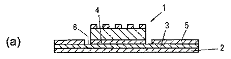
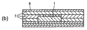
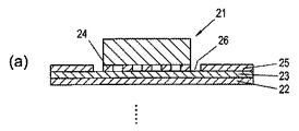
- 少なくとも1つの電子部品をプリント基板又はプリント基板中間体に集積する方法であって、以下の工程:
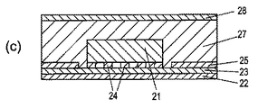
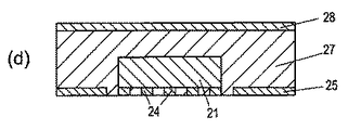
− 電子部品(1、21、31、41、51)を少なくとも暫定的に支持するための層(2、22、32、42、52)を提供し、
− 前記層(2、22、32、42、52)上に前記電子部品(1、21、31、41、51)を固定し、そのとき前記電子部品(21、41)の接点(24、23)又は前記電子部品(1、3)の表面に配置された導電層(4、34)が支持層(2、22、32、42、52)に配向され、
− 導電層(5、25、35、45、53)を、固定されるべき前記電子部品(1、21、31、41、51)及び/又は前記部品(21、41)の前記支持層に向けられた前記接点(24、43)の寸法と一致した少なくとも1つの隙間(6、26、38、46、60)とともに、前記支持層上(51)に配置し、
− 前記支持層に固定される前記部品(1、21、31、41、51)及び、前記部品(1、21、31、41、51)に近接し、前記支持層(2、22,32,42,52)上に配置された前記導電層(5、25、35、45、53)の少なくとも部分領域を、例えばプリプレグシート及び/又は樹脂のような絶縁素材(7、9、27、36、48、54、55)で少なくとも部分的に包囲或いは被覆し、
− 前記電子部品の前記接点(24、43)又は前記導電層(4、34)、及び前記部品に近接し、前記支持層(2、22、32、42、52)上に配置された前記導電層(5、25、35、45)の少なくとも部分領域を、前記支持層(2、22、32、42)の除去後に或いは除去によって露出し、
− 前記電子部品(1、21、31、41、51)の前記接点(24、43)又は前記導電層(4、34)を前記部品に近接する前記導電層(5、25、35、45、53)と少なくとも部分的に接触させる、を含む方法。 - 前記電子部品(1、21、31、41、51)が前記支持層(2、22、32、42、52)上に、接着剤(3、23、33、44)、接着箔、部品の接着膜などを介して固定されることを特徴とする請求項1に記載の方法。
- 前記接着層(3、23、33、44)又は接着箔、又は膜(K)が最大15μm、特に約0.1から10μmの厚さに形成されることを特徴とする請求項2に記載された方法。
- 接着層が、インクジェット、フレックス、凹版又はオフセット印刷によって塗着されることを特徴とする請求項1、2又は3に記載の方法。
- 前記部品(1、21、31、41、51)に近接する前記導電層(5、25、35、45、53)が金属箔、特に銅箔によって形成されることを特徴とする請求項1から4のいずれか一項に記載の方法。
- 金属箔(25、45)、特に銅箔が、特に導電性構造のために、最大で15μm、特に約0.1から10μmの厚さに形成されることを特徴とする請求項5に記載の方法。
- 前記金属箔(35)、特に銅箔が、特に放熱のために、最大500μm、特に約35から400μmの厚さに形成されることを特徴とする請求項5に記載の方法。
- 前記部品(21、41)に近接する前記導電層(25、45)が構造化された層で形成されることを特徴とする請求項1から7のいずれか一項に記載の方法。
- 前記支持層(22、42)に向けられた前記電子部品(21、41)の前記接点(24、43)において、前記支持層(22、42)が除去された後、前記接点(24、43)が構造化された前記導電層と接触或いは接続することを特徴とする請求項8に記載の方法。
- 前記電子部品(1、31)の前記導電層(4、34)の露出後、それに近接する前記導電層(5、35)と実質的に全面接触が行われることを特徴とする請求項1から7のいずれか一項に記載の方法。
- 導電性素材、特に熱伝導性素材から成る層(12)の全面接触がなされることを特徴とする請求項10に記載の方法。
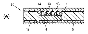
- 前記電子部品(1、21、31、41)の前記導電層(5、35)又は前記接点(24、43)の露出後及び、それに近接する前記導電層(5、25、35、45)との接触後、更なる層(12、13、29、30、57)及び/又はプリント基板の構造化が形成される或いは行われることを特徴とする請求項1から11のいずれか一項に記載の方法。
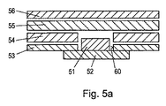
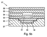
- プリント基板の少なくとも1枚の更なる層(57)が 凹部或いは溝(59)を集積された前記電子部品(51)の領域内に設けることを特徴とする請求項12に記載の方法。
- 例えばプリプレグシート及び/又は樹脂のような絶縁素材によって少なくとも部分的に包囲された、或いはそれによって被覆された電子部品(1、21、31、41、51)及び、前記電子部品(21、41)の接点(24、43)又は前記電子部品(1,31)表面の導電層の高さに配置され、前記部品に近接する導電層(5、25、35、45、53)から成るプリント基板又はプリント基板中間体であって、そのとき前記部品に近接する前記導電層が少なくとも1つの、固定されるべき前記電子部品(1、21、31、41、51)及び/又はそれと連結されるべき前記電子部品(21、41)の前記接点(24、43)の寸法と一致した隙間(6、26、38、46、60)を備え、そのとき前記電子部品(21、41)の前記接点(24、43)又は前記電子部品(1、31)の表面に配置された前記導電層(5、35)が、前記部品に近接した前記導電層(5、25、35、45)と連結されるか、或いは連結可能であることを特徴とするプリント基板又はプリント基板中間体。
- 前記部品(1、21、31、41、51)に近接する前記導電層(5、25、35、45、53)が金属箔、特に銅箔によって形成されることを特徴とする請求項14に記載されたプリント基板又はプリント基板中間体。
- 前記金属箔(25、45)、特に銅箔が、特に導電性構造のために、最大で15μm、特に約0.1から10μmの厚さを有することを特徴とする請求項15に記載のプリント基板又はプリント基板中間体。
- 前記金属箔(35)、特に銅箔が、特に放熱のために最大500μm、特に約35から400μmの厚さを有することを特徴とする請求項15に記載のプリント基板又はプリント基板中間体。
- 前記電子部品(21、41)の接点(24、43)との連結或いは接触のために、前記部品(21、41)に近接する前記導電層が構造化された導電層(25、45)によって形成されていることを特徴とする、請求項14から17のいずれか一項に記載のプリント基板又はプリント基板中間体。
- 前記電子部品(1、31)の前記導電層(4、34)との連結或いは接触のために、それに近接する前記導電層(5、35)と実質的に全面接触が行われることを特徴とする、請求項14から17のいずれか一項に記載のプリント基板又はプリント基板中間体。
- 導電性素材、特に熱伝導性素材からなる層(5、35)の全面接触がなされることを特徴とする請求項19に記載のプリント基板又はプリント基板中間体。
Applications Claiming Priority (3)
| Application Number | Priority Date | Filing Date | Title |
|---|---|---|---|
| ATGM41/2011U AT13055U1 (de) | 2011-01-26 | 2011-01-26 | Verfahren zur integration eines elektronischen bauteils in eine leiterplatte oder ein leiterplatten-zwischenprodukt sowie leiterplatte oder leiterplatten-zwischenprodukt |
| ATGM41/2011 | 2011-01-26 | ||
| PCT/AT2012/000011 WO2012100274A1 (de) | 2011-01-26 | 2012-01-24 | Verfahren zur integration eines elektronischen bauteils in eine leiterplatte oder ein leiterplatten-zwischenprodukt sowie leiterplatte oder leiterplatten-zwischenprodukt |
Publications (2)
| Publication Number | Publication Date |
|---|---|
| JP2014505367A true JP2014505367A (ja) | 2014-02-27 |
| JP5988178B2 JP5988178B2 (ja) | 2016-09-07 |
Family
ID=46579374
Family Applications (1)
| Application Number | Title | Priority Date | Filing Date |
|---|---|---|---|
| JP2013550705A Active JP5988178B2 (ja) | 2011-01-26 | 2012-01-24 | 電子部品のプリント基板又はプリント基板の中間生成物への集積方法及びプリント基板又はプリント基板の中間生成物 |
Country Status (6)
| Country | Link |
|---|---|
| US (1) | US9253888B2 (ja) |
| EP (1) | EP2668835B1 (ja) |
| JP (1) | JP5988178B2 (ja) |
| CN (2) | CN107426914B (ja) |
| AT (1) | AT13055U1 (ja) |
| WO (1) | WO2012100274A1 (ja) |
Families Citing this family (19)
| Publication number | Priority date | Publication date | Assignee | Title |
|---|---|---|---|---|
| AT13055U1 (de) * | 2011-01-26 | 2013-05-15 | Austria Tech & System Tech | Verfahren zur integration eines elektronischen bauteils in eine leiterplatte oder ein leiterplatten-zwischenprodukt sowie leiterplatte oder leiterplatten-zwischenprodukt |
| CN203206586U (zh) * | 2013-02-27 | 2013-09-18 | 奥特斯(中国)有限公司 | 用于生产印制电路板的半成品 |
| AT514074B1 (de) | 2013-04-02 | 2014-10-15 | Austria Tech & System Tech | Verfahren zum Herstellen eines Leiterplattenelements |
| AT514564B1 (de) * | 2013-07-04 | 2015-02-15 | Austria Tech & System Tech | Verfahren zum Ankontaktieren und Umverdrahten |
| US10219384B2 (en) | 2013-11-27 | 2019-02-26 | At&S Austria Technologie & Systemtechnik Aktiengesellschaft | Circuit board structure |
| AT515101B1 (de) | 2013-12-12 | 2015-06-15 | Austria Tech & System Tech | Verfahren zum Einbetten einer Komponente in eine Leiterplatte |
| JP2015146346A (ja) * | 2014-01-31 | 2015-08-13 | イビデン株式会社 | 多層配線板 |
| AT515447B1 (de) | 2014-02-27 | 2019-10-15 | At & S Austria Tech & Systemtechnik Ag | Verfahren zum Kontaktieren eines in eine Leiterplatte eingebetteten Bauelements sowie Leiterplatte |
| US11523520B2 (en) | 2014-02-27 | 2022-12-06 | At&S Austria Technologie & Systemtechnik Aktiengesellschaft | Method for making contact with a component embedded in a printed circuit board |
| GB2524791B (en) * | 2014-04-02 | 2018-10-03 | At & S Austria Tech & Systemtechnik Ag | Placement of component in circuit board intermediate product by flowable adhesive layer on carrier substrate |
| WO2016035631A1 (ja) * | 2014-09-04 | 2016-03-10 | 株式会社村田製作所 | 部品内蔵基板 |
| TWI611523B (zh) * | 2014-09-05 | 2018-01-11 | 矽品精密工業股份有限公司 | 半導體封裝件之製法 |
| KR102194718B1 (ko) * | 2014-10-13 | 2020-12-23 | 삼성전기주식회사 | 임베디드 기판 및 임베디드 기판의 제조 방법 |
| US20170084594A1 (en) * | 2015-09-20 | 2017-03-23 | Qualcomm Incorporated | Embedding die technology |
| EP3206229B1 (en) | 2016-02-09 | 2020-10-07 | AT & S Austria Technologie & Systemtechnik Aktiengesellschaft | Methods of manufacturing flexible electronic devices |
| EP3300105B1 (de) * | 2016-09-26 | 2022-07-13 | Infineon Technologies AG | Leistungshalbleitermodul und verfahren zur herstellung eines leistungshalbleitermoduls |
| CN207022286U (zh) * | 2017-01-13 | 2018-02-16 | 奥特斯(中国)有限公司 | 用于制造部件承载件的半成品及其部件承载件 |
| WO2020214520A1 (en) * | 2019-04-14 | 2020-10-22 | The Johns Hopkins University | Clutch system with phase changing materials |
| CN114793394B (zh) * | 2021-01-25 | 2025-05-27 | 礼鼎半导体科技秦皇岛有限公司 | 封装电路结构及其制作方法 |
Citations (5)
| Publication number | Priority date | Publication date | Assignee | Title |
|---|---|---|---|---|
| JP2006261246A (ja) * | 2005-03-15 | 2006-09-28 | Shinko Electric Ind Co Ltd | 配線基板および配線基板の製造方法 |
| JP2008544511A (ja) * | 2005-06-16 | 2008-12-04 | イムベラ エレクトロニクス オサケユキチュア | 回路基板構造の製造方法及び回路基板構造 |
| JP2010021423A (ja) * | 2008-07-11 | 2010-01-28 | Tdk Corp | Ic内蔵基板及びその製造方法 |
| JP2010153505A (ja) * | 2008-12-24 | 2010-07-08 | Shinko Electric Ind Co Ltd | 微細配線パッケージ及びその製造方法 |
| WO2010103695A1 (ja) * | 2009-03-09 | 2010-09-16 | 株式会社村田製作所 | 部品内蔵モジュールの製造方法及び部品内蔵モジュール |
Family Cites Families (14)
| Publication number | Priority date | Publication date | Assignee | Title |
|---|---|---|---|---|
| FI119215B (fi) | 2002-01-31 | 2008-08-29 | Imbera Electronics Oy | Menetelmä komponentin upottamiseksi alustaan ja elektroniikkamoduuli |
| FI115285B (fi) | 2002-01-31 | 2005-03-31 | Imbera Electronics Oy | Menetelmä komponentin upottamiseksi alustaan ja kontaktin muodostamiseksi |
| JP2004055991A (ja) * | 2002-07-23 | 2004-02-19 | Ngk Spark Plug Co Ltd | 配線基板 |
| FI119583B (fi) | 2003-02-26 | 2008-12-31 | Imbera Electronics Oy | Menetelmä elektroniikkamoduulin valmistamiseksi |
| FI115601B (fi) * | 2003-04-01 | 2005-05-31 | Imbera Electronics Oy | Menetelmä elektroniikkamoduulin valmistamiseksi ja elektroniikkamoduuli |
| CN2617121Y (zh) * | 2003-04-25 | 2004-05-19 | 威盛电子股份有限公司 | 多层板的结构 |
| FI20041680A7 (fi) | 2004-04-27 | 2005-10-28 | Imbera Electronics Oy | Elektroniikkamoduuli ja menetelmä sen valmistamiseksi |
| FI117814B (fi) * | 2004-06-15 | 2007-02-28 | Imbera Electronics Oy | Menetelmä elektroniikkamoduulin valmistamiseksi |
| FI117369B (fi) * | 2004-11-26 | 2006-09-15 | Imbera Electronics Oy | Menetelmä elektroniikkamoduulin valmistamiseksi |
| KR100704936B1 (ko) | 2005-06-22 | 2007-04-09 | 삼성전기주식회사 | 전자부품 내장 인쇄회로기판 및 그 제작방법 |
| US20100044845A1 (en) * | 2006-04-27 | 2010-02-25 | Nec Corporation | Circuit substrate, an electronic device arrangement and a manufacturing process for the circuit substrate |
| JP2009224379A (ja) * | 2008-03-13 | 2009-10-01 | Renesas Technology Corp | 半導体装置およびその製造方法 |
| AT12316U1 (de) * | 2008-10-30 | 2012-03-15 | Austria Tech & System Tech | Verfahren zur integration eines elektronischen bauteils in eine leiterplatte |
| AT13055U1 (de) * | 2011-01-26 | 2013-05-15 | Austria Tech & System Tech | Verfahren zur integration eines elektronischen bauteils in eine leiterplatte oder ein leiterplatten-zwischenprodukt sowie leiterplatte oder leiterplatten-zwischenprodukt |
-
2011
- 2011-01-26 AT ATGM41/2011U patent/AT13055U1/de not_active IP Right Cessation
-
2012
- 2012-01-24 US US13/980,383 patent/US9253888B2/en active Active
- 2012-01-24 WO PCT/AT2012/000011 patent/WO2012100274A1/de not_active Ceased
- 2012-01-24 EP EP12709271.6A patent/EP2668835B1/de active Active
- 2012-01-24 JP JP2013550705A patent/JP5988178B2/ja active Active
- 2012-01-24 CN CN201710570832.0A patent/CN107426914B/zh active Active
- 2012-01-24 CN CN201280006766.XA patent/CN103348777B/zh active Active
Patent Citations (5)
| Publication number | Priority date | Publication date | Assignee | Title |
|---|---|---|---|---|
| JP2006261246A (ja) * | 2005-03-15 | 2006-09-28 | Shinko Electric Ind Co Ltd | 配線基板および配線基板の製造方法 |
| JP2008544511A (ja) * | 2005-06-16 | 2008-12-04 | イムベラ エレクトロニクス オサケユキチュア | 回路基板構造の製造方法及び回路基板構造 |
| JP2010021423A (ja) * | 2008-07-11 | 2010-01-28 | Tdk Corp | Ic内蔵基板及びその製造方法 |
| JP2010153505A (ja) * | 2008-12-24 | 2010-07-08 | Shinko Electric Ind Co Ltd | 微細配線パッケージ及びその製造方法 |
| WO2010103695A1 (ja) * | 2009-03-09 | 2010-09-16 | 株式会社村田製作所 | 部品内蔵モジュールの製造方法及び部品内蔵モジュール |
Also Published As
| Publication number | Publication date |
|---|---|
| CN107426914A (zh) | 2017-12-01 |
| US20140000941A1 (en) | 2014-01-02 |
| WO2012100274A1 (de) | 2012-08-02 |
| US9253888B2 (en) | 2016-02-02 |
| JP5988178B2 (ja) | 2016-09-07 |
| EP2668835A1 (de) | 2013-12-04 |
| CN103348777A (zh) | 2013-10-09 |
| CN107426914B (zh) | 2021-01-08 |
| AT13055U1 (de) | 2013-05-15 |
| EP2668835B1 (de) | 2014-10-22 |
| CN103348777B (zh) | 2017-07-28 |
Similar Documents
| Publication | Publication Date | Title |
|---|---|---|
| JP5988178B2 (ja) | 電子部品のプリント基板又はプリント基板の中間生成物への集積方法及びプリント基板又はプリント基板の中間生成物 | |
| CN102090155B (zh) | 用于将至少一个电子构件集成到印制线路板中的方法以及印制线路板 | |
| CN102204418B (zh) | 用于将电子部件集成到印制电路板中的方法 | |
| US9024203B2 (en) | Embedded printed circuit board and method for manufacturing same | |
| JPWO2010018708A1 (ja) | 部品内蔵モジュールの製造方法及び部品内蔵モジュール | |
| KR101755814B1 (ko) | 반도체 장치 및 그의 제조방법 | |
| CN105393649B (zh) | 用于制造印刷电路板元件的方法 | |
| CN201238050Y (zh) | 包含印制电路板和至少一个电子构件的系统 | |
| KR101905879B1 (ko) | 인쇄회로기판 및 그의 제조 방법 | |
| US8677615B2 (en) | Method for embedding electrical components | |
| JP6099902B2 (ja) | 配線基板の製造方法 | |
| JP5185622B2 (ja) | 多層配線基板 | |
| JP4470452B2 (ja) | 配線基板の製造方法 | |
| JP4514538B2 (ja) | 回路装置およびその製造方法 | |
| JP2008244336A (ja) | プリント配線板の製造方法、及びプリント配線板 | |
| KR20070013634A (ko) | 다층 인쇄회로기판의 제조방법 | |
| JP2004140171A (ja) | 多層プリント基板、多層プリント基板の放熱構造および多層プリント基板の製造方法 | |
| JP2005353751A (ja) | プリント配線基板 | |
| JP5067607B2 (ja) | 張合せ基板 | |
| JP5360404B2 (ja) | 部品内蔵基板の製造方法 | |
| JP2019091778A (ja) | 半導体装置用基板およびそれを用いた半導体装置の製造方法 | |
| JPH1075058A (ja) | セラミック基板とその製造方法 | |
| JP2008047613A (ja) | 積層セラミック基板に表面実装部品の固定部を形成する方法及び、その固定部に表面実装部品を固定する方法、並びに、これらの方法に用いる積層セラミック基板 | |
| JP2009064887A (ja) | プリント配線板 | |
| KR20120033808A (ko) | 인쇄회로기판 및 그의 제조 방법 |
Legal Events
| Date | Code | Title | Description |
|---|---|---|---|
| A621 | Written request for application examination |
Free format text: JAPANESE INTERMEDIATE CODE: A621 Effective date: 20150123 |
|
| A521 | Request for written amendment filed |
Free format text: JAPANESE INTERMEDIATE CODE: A523 Effective date: 20150325 |
|
| A977 | Report on retrieval |
Free format text: JAPANESE INTERMEDIATE CODE: A971007 Effective date: 20151023 |
|
| A131 | Notification of reasons for refusal |
Free format text: JAPANESE INTERMEDIATE CODE: A131 Effective date: 20151110 |
|
| A601 | Written request for extension of time |
Free format text: JAPANESE INTERMEDIATE CODE: A601 Effective date: 20160209 |
|
| A521 | Request for written amendment filed |
Free format text: JAPANESE INTERMEDIATE CODE: A523 Effective date: 20160303 |
|
| TRDD | Decision of grant or rejection written | ||
| A01 | Written decision to grant a patent or to grant a registration (utility model) |
Free format text: JAPANESE INTERMEDIATE CODE: A01 Effective date: 20160705 |
|
| A61 | First payment of annual fees (during grant procedure) |
Free format text: JAPANESE INTERMEDIATE CODE: A61 Effective date: 20160728 |
|
| R150 | Certificate of patent or registration of utility model |
Ref document number: 5988178 Country of ref document: JP Free format text: JAPANESE INTERMEDIATE CODE: R150 |
|
| R250 | Receipt of annual fees |
Free format text: JAPANESE INTERMEDIATE CODE: R250 |
|
| R250 | Receipt of annual fees |
Free format text: JAPANESE INTERMEDIATE CODE: R250 |
|
| R250 | Receipt of annual fees |
Free format text: JAPANESE INTERMEDIATE CODE: R250 |
|
| R250 | Receipt of annual fees |
Free format text: JAPANESE INTERMEDIATE CODE: R250 |
|
| R250 | Receipt of annual fees |
Free format text: JAPANESE INTERMEDIATE CODE: R250 |
|
| R250 | Receipt of annual fees |
Free format text: JAPANESE INTERMEDIATE CODE: R250 |
|
| R250 | Receipt of annual fees |
Free format text: JAPANESE INTERMEDIATE CODE: R250 |
|
| R250 | Receipt of annual fees |
Free format text: JAPANESE INTERMEDIATE CODE: R250 |