JP2015015497A - 放射放出半導体チップ - Google Patents
放射放出半導体チップ Download PDFInfo
- Publication number
- JP2015015497A JP2015015497A JP2014193756A JP2014193756A JP2015015497A JP 2015015497 A JP2015015497 A JP 2015015497A JP 2014193756 A JP2014193756 A JP 2014193756A JP 2014193756 A JP2014193756 A JP 2014193756A JP 2015015497 A JP2015015497 A JP 2015015497A
- Authority
- JP
- Japan
- Prior art keywords
- semiconductor
- layer
- region
- semiconductor chip
- connection layer
- Prior art date
- Legal status (The legal status is an assumption and is not a legal conclusion. Google has not performed a legal analysis and makes no representation as to the accuracy of the status listed.)
- Granted
Links
Images


Classifications
-
- H—ELECTRICITY
- H10—SEMICONDUCTOR DEVICES; ELECTRIC SOLID-STATE DEVICES NOT OTHERWISE PROVIDED FOR
- H10H—INORGANIC LIGHT-EMITTING SEMICONDUCTOR DEVICES HAVING POTENTIAL BARRIERS
- H10H29/00—Integrated devices, or assemblies of multiple devices, comprising at least one light-emitting semiconductor element covered by group H10H20/00
- H10H29/10—Integrated devices comprising at least one light-emitting semiconductor component covered by group H10H20/00
-
- H—ELECTRICITY
- H10—SEMICONDUCTOR DEVICES; ELECTRIC SOLID-STATE DEVICES NOT OTHERWISE PROVIDED FOR
- H10D—INORGANIC ELECTRIC SEMICONDUCTOR DEVICES
- H10D89/00—Aspects of integrated devices not covered by groups H10D84/00 - H10D88/00
- H10D89/60—Integrated devices comprising arrangements for electrical or thermal protection, e.g. protection circuits against electrostatic discharge [ESD]
- H10D89/601—Integrated devices comprising arrangements for electrical or thermal protection, e.g. protection circuits against electrostatic discharge [ESD] for devices having insulated gate electrodes, e.g. for IGFETs or IGBTs
- H10D89/611—Integrated devices comprising arrangements for electrical or thermal protection, e.g. protection circuits against electrostatic discharge [ESD] for devices having insulated gate electrodes, e.g. for IGFETs or IGBTs using diodes as protective elements
-
- H—ELECTRICITY
- H10—SEMICONDUCTOR DEVICES; ELECTRIC SOLID-STATE DEVICES NOT OTHERWISE PROVIDED FOR
- H10H—INORGANIC LIGHT-EMITTING SEMICONDUCTOR DEVICES HAVING POTENTIAL BARRIERS
- H10H20/00—Individual inorganic light-emitting semiconductor devices having potential barriers, e.g. light-emitting diodes [LED]
- H10H20/01—Manufacture or treatment
-
- H—ELECTRICITY
- H10—SEMICONDUCTOR DEVICES; ELECTRIC SOLID-STATE DEVICES NOT OTHERWISE PROVIDED FOR
- H10H—INORGANIC LIGHT-EMITTING SEMICONDUCTOR DEVICES HAVING POTENTIAL BARRIERS
- H10H20/00—Individual inorganic light-emitting semiconductor devices having potential barriers, e.g. light-emitting diodes [LED]
- H10H20/01—Manufacture or treatment
- H10H20/032—Manufacture or treatment of electrodes
-
- H—ELECTRICITY
- H10—SEMICONDUCTOR DEVICES; ELECTRIC SOLID-STATE DEVICES NOT OTHERWISE PROVIDED FOR
- H10H—INORGANIC LIGHT-EMITTING SEMICONDUCTOR DEVICES HAVING POTENTIAL BARRIERS
- H10H20/00—Individual inorganic light-emitting semiconductor devices having potential barriers, e.g. light-emitting diodes [LED]
- H10H20/80—Constructional details
- H10H20/81—Bodies
- H10H20/813—Bodies having a plurality of light-emitting regions, e.g. multi-junction LEDs or light-emitting devices having photoluminescent regions within the bodies
-
- H—ELECTRICITY
- H10—SEMICONDUCTOR DEVICES; ELECTRIC SOLID-STATE DEVICES NOT OTHERWISE PROVIDED FOR
- H10H—INORGANIC LIGHT-EMITTING SEMICONDUCTOR DEVICES HAVING POTENTIAL BARRIERS
- H10H20/00—Individual inorganic light-emitting semiconductor devices having potential barriers, e.g. light-emitting diodes [LED]
- H10H20/80—Constructional details
- H10H20/83—Electrodes
- H10H20/831—Electrodes characterised by their shape
-
- H—ELECTRICITY
- H10—SEMICONDUCTOR DEVICES; ELECTRIC SOLID-STATE DEVICES NOT OTHERWISE PROVIDED FOR
- H10H—INORGANIC LIGHT-EMITTING SEMICONDUCTOR DEVICES HAVING POTENTIAL BARRIERS
- H10H20/00—Individual inorganic light-emitting semiconductor devices having potential barriers, e.g. light-emitting diodes [LED]
- H10H20/80—Constructional details
- H10H20/83—Electrodes
- H10H20/831—Electrodes characterised by their shape
- H10H20/8312—Electrodes characterised by their shape extending at least partially through the bodies
-
- H—ELECTRICITY
- H10—SEMICONDUCTOR DEVICES; ELECTRIC SOLID-STATE DEVICES NOT OTHERWISE PROVIDED FOR
- H10H—INORGANIC LIGHT-EMITTING SEMICONDUCTOR DEVICES HAVING POTENTIAL BARRIERS
- H10H20/00—Individual inorganic light-emitting semiconductor devices having potential barriers, e.g. light-emitting diodes [LED]
- H10H20/80—Constructional details
- H10H20/85—Packages
- H10H20/857—Interconnections, e.g. lead-frames, bond wires or solder balls
-
- H—ELECTRICITY
- H10—SEMICONDUCTOR DEVICES; ELECTRIC SOLID-STATE DEVICES NOT OTHERWISE PROVIDED FOR
- H10H—INORGANIC LIGHT-EMITTING SEMICONDUCTOR DEVICES HAVING POTENTIAL BARRIERS
- H10H20/00—Individual inorganic light-emitting semiconductor devices having potential barriers, e.g. light-emitting diodes [LED]
- H10H20/80—Constructional details
- H10H20/81—Bodies
-
- H—ELECTRICITY
- H10—SEMICONDUCTOR DEVICES; ELECTRIC SOLID-STATE DEVICES NOT OTHERWISE PROVIDED FOR
- H10W—GENERIC PACKAGES, INTERCONNECTIONS, CONNECTORS OR OTHER CONSTRUCTIONAL DETAILS OF DEVICES COVERED BY CLASS H10
- H10W90/00—Package configurations
Landscapes
- Led Device Packages (AREA)
- Led Devices (AREA)
Abstract
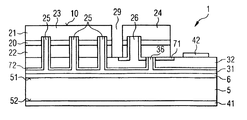
【解決手段】放射放出半導体チップ1は、キャリア5と半導体積層体を有する半導体ボディ2とを備える。半導体積層体を有する半導体ボディには、放出領域23および保護ダイオード領域24が形成されている。半導体積層体は、放射を発生するために設けられている活性領域20を備えており、この活性領域は、第1の半導体層21と第2の半導体層22との間に配置されている。第1の半導体層は、キャリアとは反対側の活性領域の面に配置されている。放出領域は、活性領域を貫いて延在する凹部25を有する。第1の半導体層は、放出領域においては、第1の接続層に導電接続されており、この第1の接続層31は、第1の半導体層から凹部の中をキャリアの方向に延在している。第1の接続層は、保護ダイオード領域においては、第2の半導体層に導電接続されている。
【選択図】図2
Description
− 放射を発生させるエピタキシャル積層体の第1の主領域(キャリア要素(例えばキャリア)に面している主領域)に、反射層が堆積または形成されており、この反射層が、エピタキシャル積層体において発生する電磁放射の少なくとも一部分を、エピタキシャル積層体中に反射する。
− エピタキシャル積層体の厚さは、20μm以下の範囲、特に10μm以下の範囲である。
− エピタキシャル積層体は、少なくとも一領域が混合構造(intermixing structure)である少なくとも1層の半導体層を含んでおり、この混合構造によって、理想的にはエピタキシャル積層体における近似的に光のエルゴード分布につながり、すなわち、この混合構造は、実質的にエルゴード的確率過程である散乱挙動を有する。
Claims (15)
- キャリア(5)と、半導体積層体を有する半導体ボディ(2)と、を備えている放射放出半導体チップ(1)であって、
− 前記半導体積層体を有する前記半導体ボディ(2)に、放出領域(23)および保護ダイオード領域(24)が形成されており、
− 前記半導体積層体が、放射を発生させるために設けられている活性領域(20)を備えており、前記活性領域が、第1の半導体層(21)と第2の半導体層(22)との間に配置されており、
− 前記第1の半導体層(21)が、前記キャリア(5)とは反対側の前記活性領域(20)の面に配置されており、
− 前記放出領域(23)が、前記活性領域(20)を貫いて延在する凹部(25)を有し、
− 前記第1の半導体層(21)が、前記放出領域(23)において、第1の接続層(31)に導電接続されており、前記第1の接続層(31)が、前記第1の半導体層(21)から前記凹部(25)の中を前記キャリア(5)の方向に延在しており、
− 前記第1の接続層(31)が、前記保護ダイオード領域(24)において、前記第2の半導体層(22)に導電接続されており、
− 前記第2の半導体層(22)が、前記放出領域(23)において、前記第2の接続層(32)に導電接続されており、
− 前記第2の接続層(32)は、部分的に前記半導体ボディ(2)と前記キャリア(5)との間に延在している、
放射放出半導体チップ。 - 前記放出領域と前記保護ダイオード領域が、それぞれの順方向に関して互いに逆並列に接続されている、
請求項1に記載の半導体チップ。 - 前記放出領域および前記保護ダイオード領域が、横方向に互いに並んで配置されている、前記半導体ボディの領域である、
請求項1または請求項2に記載の半導体チップ。 - 前記半導体ボディが前記キャリアに接着結合されており、前記第1の接続層が、部分的に前記半導体ボディと前記キャリアとの間に延在している、
請求項1から請求項3のいずれかに記載の半導体チップ。 - 前記第2の接続層が、部分的に前記放出領域と前記第1の接続層との間に延在している、
請求項1から請求項4のいずれかに記載の半導体チップ。 - 前記第2の接続層が、前記保護ダイオード領域において、前記第1の半導体層に導電接続されている、
請求項1から請求項5のいずれかに記載の半導体チップ。 - 前記保護ダイオード領域がさらなる凹部(26)を有し、前記第2の接続層が、前記第1の半導体層から前記さらなる凹部の中を前記キャリアの方向に延在している、
請求項1から請求項6のいずれかに記載の半導体チップ。 - 前記第2の接続層を外部から接触接続するために設けられているコンタクト(42)、
を有する、
請求項1から請求項7のいずれかに記載の半導体チップ。 - 前記コンタクトがコンタクト層(420)によって形成されており、前記コンタクト層(420)の少なくとも一部分が、前記保護ダイオード領域を横方向に画定している側面領域(240)を覆っている、
請求項8に記載の半導体チップ。 - 前記コンタクトが、前記半導体チップの平面視において、前記保護ダイオード領域を少なくとも部分的に覆っている、
請求項9に記載の半導体チップ。 - 前記コンタクトおよび前記保護ダイオード領域が、前記半導体チップの平面視において互いに並んで配置されている、
請求項8に記載の半導体チップ。 - 前記第1の接続層は、前記半導体チップの平面視において前記キャリアを完全に覆っている、
請求項1から請求項11のいずれかに記載の半導体チップ。 - 複数の放射放出半導体チップ(1)を製造する方法であって、
a)放射を発生させるために設けられる活性領域(20)を有する半導体積層体(2)を形成するステップであって、前記活性領域が、第1の半導体層(21)と第2の半導体層(22)との間に配置されている、前記ステップと、
b)前記第2の半導体層(22)および前記活性領域(20)を貫いて延在する複数の凹部(25)を形成するステップと、
c)前記半導体積層体(2)上に第1の接続層(31)を形成するステップであって、前記第1の接続層(31)が、前記凹部(25)において、前記第1の半導体層(21)に導電接続されており、前記第1の接続層(31)が、部分的に前記第2の半導体層(22)に導電接続されている、前記ステップと、
d)前記半導体積層体(2)とキャリア(5)とを備えている集合体(9)を形成するステップと、
e)前記半導体積層体(2)から複数の放出領域(23)および複数の保護ダイオード領域(24)を形成するステップであって、前記放出領域(23)それぞれが少なくとも1つの凹部(25)を有し、前記保護ダイオード領域(24)それぞれにおいて、前記第1の接続層(31)が前記第2の半導体層(22)に導電接続されている、前記ステップと、
f)前記集合体(9)を複数の半導体チップ(1)に個片化するステップと、
を含んでおり、
− 半導体チップ(1)それぞれが少なくとも1つの放出領域(23)と少なくとも1つの保護ダイオード領域(24)とを有し、
− 前記第2の半導体層(22)が、前記放出領域(23)において、前記第2の接続層(32)に導電接続されており、
− 前記第2の接続層(32)は、部分的に前記半導体ボディ(2)と前記キャリア(5)との間に延在している、
方法。 - ステップe)の前に、前記半導体積層体のための成長基板(8)を少なくとも部分的に除去する、
請求項13に記載の方法。 - 請求項1から請求項12のいずれかに記載の複数の半導体チップが製造される、
請求項13または請求項14に記載の方法。
Applications Claiming Priority (4)
| Application Number | Priority Date | Filing Date | Title |
|---|---|---|---|
| DE102008059580.2 | 2008-11-28 | ||
| DE102008059580 | 2008-11-28 | ||
| DE102009006177.0 | 2009-01-26 | ||
| DE102009006177A DE102009006177A1 (de) | 2008-11-28 | 2009-01-26 | Strahlungsemittierender Halbleiterchip |
Related Parent Applications (1)
| Application Number | Title | Priority Date | Filing Date |
|---|---|---|---|
| JP2011537839A Division JP5669746B2 (ja) | 2008-11-28 | 2009-10-29 | 放射放出半導体チップ |
Publications (2)
| Publication Number | Publication Date |
|---|---|
| JP2015015497A true JP2015015497A (ja) | 2015-01-22 |
| JP5890498B2 JP5890498B2 (ja) | 2016-03-22 |
Family
ID=42134160
Family Applications (2)
| Application Number | Title | Priority Date | Filing Date |
|---|---|---|---|
| JP2011537839A Expired - Fee Related JP5669746B2 (ja) | 2008-11-28 | 2009-10-29 | 放射放出半導体チップ |
| JP2014193756A Expired - Fee Related JP5890498B2 (ja) | 2008-11-28 | 2014-09-24 | 放射放出半導体チップ |
Family Applications Before (1)
| Application Number | Title | Priority Date | Filing Date |
|---|---|---|---|
| JP2011537839A Expired - Fee Related JP5669746B2 (ja) | 2008-11-28 | 2009-10-29 | 放射放出半導体チップ |
Country Status (8)
| Country | Link |
|---|---|
| US (2) | US9054016B2 (ja) |
| EP (1) | EP2351079B1 (ja) |
| JP (2) | JP5669746B2 (ja) |
| KR (1) | KR101679092B1 (ja) |
| CN (1) | CN102227807B (ja) |
| DE (1) | DE102009006177A1 (ja) |
| TW (1) | TWI433309B (ja) |
| WO (1) | WO2010060404A1 (ja) |
Families Citing this family (49)
| Publication number | Priority date | Publication date | Assignee | Title |
|---|---|---|---|---|
| DE102008022942A1 (de) * | 2008-05-09 | 2009-11-12 | Osram Opto Semiconductors Gmbh | Strahlungsemittierender Halbleiterchip |
| DE102008051048A1 (de) * | 2008-10-09 | 2010-04-15 | Osram Opto Semiconductors Gmbh | Optoelektronischer Halbleiterkörper |
| DE102009006177A1 (de) * | 2008-11-28 | 2010-06-02 | Osram Opto Semiconductors Gmbh | Strahlungsemittierender Halbleiterchip |
| DE102010024079B4 (de) | 2010-06-17 | 2025-08-28 | OSRAM Opto Semiconductors Gesellschaft mit beschränkter Haftung | Verfahren zur Herstellung eines optoelektronischen Halbleiterchips und optoelektronischer Halbleiterchip |
| KR101154709B1 (ko) * | 2010-07-28 | 2012-06-08 | 엘지이노텍 주식회사 | 발광 소자, 발광 소자 제조방법, 발광 소자 패키지 및 조명 시스템 |
| DE102010032813A1 (de) | 2010-07-30 | 2012-02-02 | Osram Opto Semiconductors Gmbh | Verfahren zur Herstellung eines optoelektronischen Halbleiterbauteils und optoelektronisches Halbleiterbauteil |
| DE102010034665B4 (de) | 2010-08-18 | 2024-10-10 | OSRAM Opto Semiconductors Gesellschaft mit beschränkter Haftung | Optoelektronischer Halbleiterchip und Verfahren zur Herstellung von optoelektronischen Halbleiterchips |
| DE102010046792A1 (de) * | 2010-09-28 | 2012-03-29 | Osram Opto Semiconductors Gmbh | Optoelektronischer Halbleiterchip und Verfahren zu dessen Herstellung |
| DE102010056056A1 (de) * | 2010-12-23 | 2012-06-28 | Osram Opto Semiconductors Gmbh | Verfahren zur Herstellung eines elektrischen Anschlussträgers |
| JP5777879B2 (ja) | 2010-12-27 | 2015-09-09 | ローム株式会社 | 発光素子、発光素子ユニットおよび発光素子パッケージ |
| KR20120099318A (ko) * | 2011-01-26 | 2012-09-10 | 엘지이노텍 주식회사 | 발광 소자 및 그 제조방법 |
| KR101762324B1 (ko) * | 2011-01-27 | 2017-07-27 | 엘지이노텍 주식회사 | 발광 소자 |
| US8536594B2 (en) * | 2011-01-28 | 2013-09-17 | Micron Technology, Inc. | Solid state lighting devices with reduced dimensions and methods of manufacturing |
| DE102011011378B4 (de) | 2011-02-16 | 2025-10-30 | OSRAM Opto Semiconductors Gesellschaft mit beschränkter Haftung | Halbleiterchip und Verfahren zur Herstellung von Halbleiterchips |
| CN106252482B (zh) | 2011-05-25 | 2019-08-23 | 欧司朗光电半导体有限公司 | 光电子半导体芯片 |
| KR20130021300A (ko) * | 2011-08-22 | 2013-03-05 | 엘지이노텍 주식회사 | 발광소자, 발광소자 패키지, 및 라이트 유닛 |
| US8809897B2 (en) | 2011-08-31 | 2014-08-19 | Micron Technology, Inc. | Solid state transducer devices, including devices having integrated electrostatic discharge protection, and associated systems and methods |
| US9490239B2 (en) | 2011-08-31 | 2016-11-08 | Micron Technology, Inc. | Solid state transducers with state detection, and associated systems and methods |
| DE102011112000B4 (de) | 2011-08-31 | 2023-11-30 | OSRAM Opto Semiconductors Gesellschaft mit beschränkter Haftung | Leuchtdiodenchip |
| US8723206B2 (en) | 2011-09-09 | 2014-05-13 | Samsung Electronics Co., Ltd. | Semiconductor light emitting device with contact hole passing through active layer |
| EP2573827B1 (en) * | 2011-09-23 | 2018-04-18 | Samsung Electronics Co., Ltd. | Semiconductor light emitting device |
| DE102011116232B4 (de) * | 2011-10-17 | 2020-04-09 | Osram Opto Semiconductors Gmbh | Optoelektronischer Halbleiterchip und Verfahren zu dessen Herstellung |
| DE102011054891B4 (de) | 2011-10-28 | 2017-10-19 | Osram Opto Semiconductors Gmbh | Verfahren zum Durchtrennen eines Halbleiterbauelementverbunds |
| CN103094274B (zh) * | 2011-11-01 | 2016-02-10 | 三星电子株式会社 | 半导体发光装置 |
| DE102012108763B4 (de) * | 2012-09-18 | 2023-02-09 | OSRAM Opto Semiconductors Gesellschaft mit beschränkter Haftung | Optoelektronischer halbleiterchip und lichtquelle mit dem optoelektronischen halbleiterchip |
| DE102012109028A1 (de) | 2012-09-25 | 2014-03-27 | Osram Opto Semiconductors Gmbh | Optoelektronisches Halbleiterbauteil und Verfahren zur Herstellung eines optoelektronischen Halbleiterbauteils |
| DE102012110909A1 (de) * | 2012-11-13 | 2014-05-15 | Osram Opto Semiconductors Gmbh | Strahlungsemittierender Halbleiterchip und Verfahren zum Betreiben eines Halbleiterchips |
| KR20140098564A (ko) * | 2013-01-31 | 2014-08-08 | 삼성전자주식회사 | 반도체 발광소자 |
| KR102080775B1 (ko) | 2013-06-19 | 2020-02-24 | 엘지이노텍 주식회사 | 발광소자 |
| TWI661578B (zh) | 2013-06-20 | 2019-06-01 | Epistar Corporation | 發光裝置及發光陣列 |
| FR3011381B1 (fr) * | 2013-09-30 | 2017-12-08 | Aledia | Dispositif optoelectronique a diodes electroluminescentes |
| DE102013112881A1 (de) | 2013-11-21 | 2015-05-21 | Osram Opto Semiconductors Gmbh | Optoelektronischer Halbleiterchip |
| DE102014105188A1 (de) * | 2014-04-11 | 2015-10-15 | Osram Opto Semiconductors Gmbh | Halbleiterchip, optoelektronisches Bauelement mit Halbleiterchip und Verfahren zur Herstellung eines Halbleiterchips |
| DE102014116512A1 (de) * | 2014-11-12 | 2016-05-12 | Osram Opto Semiconductors Gmbh | Optoelektronisches Halbleiterbauelement und Vorrichtung mit einem optoelektronischen Halbleiterbauelement |
| JP6351531B2 (ja) * | 2015-03-23 | 2018-07-04 | 株式会社東芝 | 半導体発光素子 |
| DE102015108056A1 (de) * | 2015-05-21 | 2016-11-24 | Osram Opto Semiconductors Gmbh | Optoelektronisches Halbleiterbauteil, optoelektronische Anordnung und Verfahren zur Herstellung eines optoelektronischen Halbleiterbauteils |
| KR102388284B1 (ko) | 2015-05-26 | 2022-04-19 | 쑤저우 레킨 세미컨덕터 컴퍼니 리미티드 | 발광소자 |
| DE102015114010A1 (de) * | 2015-08-24 | 2017-03-02 | Osram Opto Semiconductors Gmbh | Optoelektronisches Bauelement, Verfahren zur Herstellung eines optoelektronischen Bauelements und Verfahren zum Betrieb eines optoelektronischen Bauelements |
| KR102378952B1 (ko) | 2015-08-27 | 2022-03-25 | 쑤저우 레킨 세미컨덕터 컴퍼니 리미티드 | 발광소자 및 이를 포함하는 발광소자 패키지 |
| DE102015116865B4 (de) | 2015-10-05 | 2025-07-10 | OSRAM Opto Semiconductors Gesellschaft mit beschränkter Haftung | Verfahren zur Herstellung eines Halbleiterchips und Halbleiterchip |
| KR102463323B1 (ko) * | 2015-11-03 | 2022-11-04 | 쑤저우 레킨 세미컨덕터 컴퍼니 리미티드 | 발광소자 및 발광소자 패키지 |
| CN105896739A (zh) * | 2016-05-19 | 2016-08-24 | 吴永良 | 一种带无线充电的门锁装置 |
| DE102016114550B4 (de) | 2016-08-05 | 2021-10-21 | OSRAM Opto Semiconductors Gesellschaft mit beschränkter Haftung | Bauelement und Verfahren zur Herstellung von Bauelementen |
| DE102017104735B4 (de) | 2017-03-07 | 2021-09-02 | OSRAM Opto Semiconductors Gesellschaft mit beschränkter Haftung | Strahlungsemittierender Halbleiterchip |
| DE102017113949A1 (de) | 2017-06-23 | 2018-12-27 | Osram Opto Semiconductors Gmbh | Verfahren zur Herstellung von optoelektronischen Halbleiterchips und optoelektronischer Halbleiterchip |
| DE102018119688B4 (de) * | 2018-08-14 | 2024-06-27 | OSRAM Opto Semiconductors Gesellschaft mit beschränkter Haftung | Optoelektronisches Halbleiterbauelement mit einem ersten Kontaktelement, welches einen ersten und einen zweiten Abschnitt aufweist sowie Verfahren zur Herstellung des optoelektronischen Halbleiterbauelements |
| JP6909983B2 (ja) * | 2018-11-29 | 2021-07-28 | 日亜化学工業株式会社 | 発光素子 |
| US12245459B2 (en) * | 2019-08-23 | 2025-03-04 | Sharp Kabushiki Kaisha | Light-emitting device including a light-emitting diode and a protective diode and display device |
| US11508715B2 (en) * | 2020-04-24 | 2022-11-22 | Creeled, Inc. | Light-emitting diode chip with electrical overstress protection |
Citations (3)
| Publication number | Priority date | Publication date | Assignee | Title |
|---|---|---|---|---|
| US20050167680A1 (en) * | 2004-02-02 | 2005-08-04 | Shih-Chang Shei | Light-emitting diode structure with electrostatic discharge protection |
| JP2007157926A (ja) * | 2005-12-02 | 2007-06-21 | Sanken Electric Co Ltd | 保護ダイオードを伴った半導体発光装置及びその製造方法 |
| WO2008131735A1 (de) * | 2007-04-26 | 2008-11-06 | Osram Opto Semiconductors Gmbh | Optoelektronischer halbleiterkörper und verfahren zur herstellung eines solchen |
Family Cites Families (20)
| Publication number | Priority date | Publication date | Assignee | Title |
|---|---|---|---|---|
| US6547249B2 (en) * | 2001-03-29 | 2003-04-15 | Lumileds Lighting U.S., Llc | Monolithic series/parallel led arrays formed on highly resistive substrates |
| KR100431760B1 (ko) | 2001-08-08 | 2004-05-17 | 삼성전기주식회사 | AlGaInN계 반도체 엘이디(LED) 소자 및 그 제조 방법 |
| US6828596B2 (en) * | 2002-06-13 | 2004-12-07 | Lumileds Lighting U.S., Llc | Contacting scheme for large and small area semiconductor light emitting flip chip devices |
| CN100358163C (zh) * | 2002-08-01 | 2007-12-26 | 日亚化学工业株式会社 | 半导体发光元件及其制造方法、使用此的发光装置 |
| DE10308866A1 (de) * | 2003-02-28 | 2004-09-09 | Osram Opto Semiconductors Gmbh | Beleuchtungsmodul und Verfahren zu dessen Herstellung |
| DE102004005269B4 (de) * | 2003-11-28 | 2005-09-29 | Osram Opto Semiconductors Gmbh | Lichtemittierendes Halbleiterbauelement mit einer Schutzdiode |
| US7279724B2 (en) | 2004-02-25 | 2007-10-09 | Philips Lumileds Lighting Company, Llc | Ceramic substrate for a light emitting diode where the substrate incorporates ESD protection |
| US7064353B2 (en) | 2004-05-26 | 2006-06-20 | Philips Lumileds Lighting Company, Llc | LED chip with integrated fast switching diode for ESD protection |
| KR100665116B1 (ko) | 2005-01-27 | 2007-01-09 | 삼성전기주식회사 | Esd 보호용 led를 구비한 질화갈륨계 발광 소자 및그 제조 방법 |
| TWI257186B (en) * | 2005-09-29 | 2006-06-21 | Formosa Epitaxy Inc | Light-emitting diode chip |
| US7994514B2 (en) * | 2006-04-21 | 2011-08-09 | Koninklijke Philips Electronics N.V. | Semiconductor light emitting device with integrated electronic components |
| US7601989B2 (en) * | 2007-03-27 | 2009-10-13 | Philips Lumileds Lighting Company, Llc | LED with porous diffusing reflector |
| KR100849826B1 (ko) * | 2007-03-29 | 2008-07-31 | 삼성전기주식회사 | 발광소자 및 이를 포함하는 패키지 |
| JP2009016467A (ja) * | 2007-07-03 | 2009-01-22 | Sony Corp | 窒化ガリウム系半導体素子及びこれを用いた光学装置並びにこれを用いた画像表示装置 |
| DE102007061479A1 (de) | 2007-12-20 | 2009-06-25 | Osram Opto Semiconductors Gmbh | Leuchtdiodenchip mit Überspannungsschutz |
| DE102008022942A1 (de) * | 2008-05-09 | 2009-11-12 | Osram Opto Semiconductors Gmbh | Strahlungsemittierender Halbleiterchip |
| DE102008034560B4 (de) * | 2008-07-24 | 2022-10-27 | OSRAM Opto Semiconductors Gesellschaft mit beschränkter Haftung | Strahlungsemittierender Halbleiterchip und Verfahren zur Herstellung eines strahlungsemittierenden Halbleiterchips |
| DE102009006177A1 (de) * | 2008-11-28 | 2010-06-02 | Osram Opto Semiconductors Gmbh | Strahlungsemittierender Halbleiterchip |
| DE102009053064A1 (de) * | 2009-11-13 | 2011-05-19 | Osram Opto Semiconductors Gmbh | Dünnfilm-Halbleiterbauelement mit Schutzdiodenstruktur und Verfahren zur Herstellung eines Dünnfilm-Halbleiterbauelements |
| DE102009056386B4 (de) * | 2009-11-30 | 2024-06-27 | OSRAM Opto Semiconductors Gesellschaft mit beschränkter Haftung | Verfahren zur Herstellung eines Halbleiterbauelements |
-
2009
- 2009-01-26 DE DE102009006177A patent/DE102009006177A1/de not_active Withdrawn
- 2009-10-29 US US13/123,421 patent/US9054016B2/en active Active
- 2009-10-29 EP EP09767932.8A patent/EP2351079B1/de active Active
- 2009-10-29 CN CN2009801478179A patent/CN102227807B/zh active Active
- 2009-10-29 KR KR1020117014630A patent/KR101679092B1/ko active Active
- 2009-10-29 WO PCT/DE2009/001524 patent/WO2010060404A1/de not_active Ceased
- 2009-10-29 JP JP2011537839A patent/JP5669746B2/ja not_active Expired - Fee Related
- 2009-11-23 TW TW098139698A patent/TWI433309B/zh not_active IP Right Cessation
-
2014
- 2014-09-24 JP JP2014193756A patent/JP5890498B2/ja not_active Expired - Fee Related
-
2015
- 2015-05-04 US US14/702,807 patent/US9590008B2/en active Active
Patent Citations (3)
| Publication number | Priority date | Publication date | Assignee | Title |
|---|---|---|---|---|
| US20050167680A1 (en) * | 2004-02-02 | 2005-08-04 | Shih-Chang Shei | Light-emitting diode structure with electrostatic discharge protection |
| JP2007157926A (ja) * | 2005-12-02 | 2007-06-21 | Sanken Electric Co Ltd | 保護ダイオードを伴った半導体発光装置及びその製造方法 |
| WO2008131735A1 (de) * | 2007-04-26 | 2008-11-06 | Osram Opto Semiconductors Gmbh | Optoelektronischer halbleiterkörper und verfahren zur herstellung eines solchen |
Also Published As
| Publication number | Publication date |
|---|---|
| TWI433309B (zh) | 2014-04-01 |
| EP2351079A1 (de) | 2011-08-03 |
| JP5669746B2 (ja) | 2015-02-12 |
| CN102227807B (zh) | 2013-10-16 |
| DE102009006177A1 (de) | 2010-06-02 |
| WO2010060404A1 (de) | 2010-06-03 |
| TW201029232A (en) | 2010-08-01 |
| US9054016B2 (en) | 2015-06-09 |
| JP5890498B2 (ja) | 2016-03-22 |
| EP2351079B1 (de) | 2017-03-08 |
| JP2012510173A (ja) | 2012-04-26 |
| US20150236070A1 (en) | 2015-08-20 |
| US20110260205A1 (en) | 2011-10-27 |
| CN102227807A (zh) | 2011-10-26 |
| KR20110095918A (ko) | 2011-08-25 |
| US9590008B2 (en) | 2017-03-07 |
| KR101679092B1 (ko) | 2016-12-06 |
Similar Documents
| Publication | Publication Date | Title |
|---|---|---|
| JP5890498B2 (ja) | 放射放出半導体チップ | |
| JP5511813B2 (ja) | 静電放電に対する保護を有する放射放出半導体チップおよびその製造方法 | |
| KR101590204B1 (ko) | 복사 방출 반도체칩 | |
| JP6104158B2 (ja) | オプトエレクトロニクス半導体チップ、およびオプトエレクトロニクス半導体チップの製造方法 | |
| KR20120099720A (ko) | 보호 다이오드 구조물을 갖는 박막 반도체 소자 그리고 박막 반도체 소자를 제조하기 위한 방법 | |
| JP5813138B2 (ja) | キャリア基板、および半導体チップの製造方法 | |
| KR20150056559A (ko) | 서로 나란히 배치되는 복수의 활성 영역을 포함한 광전자 반도체 칩 | |
| KR102550004B1 (ko) | 발광 소자 |
Legal Events
| Date | Code | Title | Description |
|---|---|---|---|
| A977 | Report on retrieval |
Free format text: JAPANESE INTERMEDIATE CODE: A971007 Effective date: 20150722 |
|
| A131 | Notification of reasons for refusal |
Free format text: JAPANESE INTERMEDIATE CODE: A131 Effective date: 20150804 |
|
| A521 | Request for written amendment filed |
Free format text: JAPANESE INTERMEDIATE CODE: A523 Effective date: 20151023 |
|
| TRDD | Decision of grant or rejection written | ||
| A01 | Written decision to grant a patent or to grant a registration (utility model) |
Free format text: JAPANESE INTERMEDIATE CODE: A01 Effective date: 20160209 |
|
| A61 | First payment of annual fees (during grant procedure) |
Free format text: JAPANESE INTERMEDIATE CODE: A61 Effective date: 20160218 |
|
| R150 | Certificate of patent or registration of utility model |
Ref document number: 5890498 Country of ref document: JP Free format text: JAPANESE INTERMEDIATE CODE: R150 |
|
| R250 | Receipt of annual fees |
Free format text: JAPANESE INTERMEDIATE CODE: R250 |
|
| R250 | Receipt of annual fees |
Free format text: JAPANESE INTERMEDIATE CODE: R250 |
|
| R250 | Receipt of annual fees |
Free format text: JAPANESE INTERMEDIATE CODE: R250 |
|
| R250 | Receipt of annual fees |
Free format text: JAPANESE INTERMEDIATE CODE: R250 |
|
| R250 | Receipt of annual fees |
Free format text: JAPANESE INTERMEDIATE CODE: R250 |
|
| R250 | Receipt of annual fees |
Free format text: JAPANESE INTERMEDIATE CODE: R250 |
|
| LAPS | Cancellation because of no payment of annual fees |