JP2015018596A - 相変化記憶材料 - Google Patents
相変化記憶材料 Download PDFInfo
- Publication number
- JP2015018596A JP2015018596A JP2014146705A JP2014146705A JP2015018596A JP 2015018596 A JP2015018596 A JP 2015018596A JP 2014146705 A JP2014146705 A JP 2014146705A JP 2014146705 A JP2014146705 A JP 2014146705A JP 2015018596 A JP2015018596 A JP 2015018596A
- Authority
- JP
- Japan
- Prior art keywords
- phase change
- change memory
- phase
- atomic percent
- thin film
- Prior art date
- Legal status (The legal status is an assumption and is not a legal conclusion. Google has not performed a legal analysis and makes no representation as to the accuracy of the status listed.)
- Granted
Links
Images


Classifications
-
- G—PHYSICS
- G11—INFORMATION STORAGE
- G11B—INFORMATION STORAGE BASED ON RELATIVE MOVEMENT BETWEEN RECORD CARRIER AND TRANSDUCER
- G11B7/00—Recording or reproducing by optical means, e.g. recording using a thermal beam of optical radiation by modifying optical properties or the physical structure, reproducing using an optical beam at lower power by sensing optical properties; Record carriers therefor
- G11B7/24—Record carriers characterised by shape, structure or physical properties, or by the selection of the material
- G11B7/241—Record carriers characterised by shape, structure or physical properties, or by the selection of the material characterised by the selection of the material
- G11B7/242—Record carriers characterised by shape, structure or physical properties, or by the selection of the material characterised by the selection of the material of recording layers
- G11B7/243—Record carriers characterised by shape, structure or physical properties, or by the selection of the material characterised by the selection of the material of recording layers comprising inorganic materials only, e.g. ablative layers
- G11B7/2433—Metals or elements of Groups 13, 14, 15 or 16 of the Periodic Table, e.g. B, Si, Ge, As, Sb, Bi, Se or Te
-
- H—ELECTRICITY
- H10—SEMICONDUCTOR DEVICES; ELECTRIC SOLID-STATE DEVICES NOT OTHERWISE PROVIDED FOR
- H10N—ELECTRIC SOLID-STATE DEVICES NOT OTHERWISE PROVIDED FOR
- H10N70/00—Solid-state devices having no potential barriers, and specially adapted for rectifying, amplifying, oscillating or switching
- H10N70/011—Manufacture or treatment of multistable switching devices
- H10N70/021—Formation of switching materials, e.g. deposition of layers
- H10N70/026—Formation of switching materials, e.g. deposition of layers by physical vapor deposition, e.g. sputtering
-
- H—ELECTRICITY
- H10—SEMICONDUCTOR DEVICES; ELECTRIC SOLID-STATE DEVICES NOT OTHERWISE PROVIDED FOR
- H10N—ELECTRIC SOLID-STATE DEVICES NOT OTHERWISE PROVIDED FOR
- H10N70/00—Solid-state devices having no potential barriers, and specially adapted for rectifying, amplifying, oscillating or switching
- H10N70/20—Multistable switching devices, e.g. memristors
- H10N70/231—Multistable switching devices, e.g. memristors based on solid-state phase change, e.g. between amorphous and crystalline phases, Ovshinsky effect
-
- H—ELECTRICITY
- H10—SEMICONDUCTOR DEVICES; ELECTRIC SOLID-STATE DEVICES NOT OTHERWISE PROVIDED FOR
- H10N—ELECTRIC SOLID-STATE DEVICES NOT OTHERWISE PROVIDED FOR
- H10N70/00—Solid-state devices having no potential barriers, and specially adapted for rectifying, amplifying, oscillating or switching
- H10N70/801—Constructional details of multistable switching devices
- H10N70/881—Switching materials
- H10N70/882—Compounds of sulfur, selenium or tellurium, e.g. chalcogenides
- H10N70/8828—Tellurides, e.g. GeSbTe
-
- G—PHYSICS
- G11—INFORMATION STORAGE
- G11B—INFORMATION STORAGE BASED ON RELATIVE MOVEMENT BETWEEN RECORD CARRIER AND TRANSDUCER
- G11B7/00—Recording or reproducing by optical means, e.g. recording using a thermal beam of optical radiation by modifying optical properties or the physical structure, reproducing using an optical beam at lower power by sensing optical properties; Record carriers therefor
- G11B7/24—Record carriers characterised by shape, structure or physical properties, or by the selection of the material
- G11B7/241—Record carriers characterised by shape, structure or physical properties, or by the selection of the material characterised by the selection of the material
- G11B7/242—Record carriers characterised by shape, structure or physical properties, or by the selection of the material characterised by the selection of the material of recording layers
- G11B7/243—Record carriers characterised by shape, structure or physical properties, or by the selection of the material characterised by the selection of the material of recording layers comprising inorganic materials only, e.g. ablative layers
- G11B2007/24302—Metals or metalloids
- G11B2007/24312—Metals or metalloids group 14 elements (e.g. Si, Ge, Sn)
-
- G—PHYSICS
- G11—INFORMATION STORAGE
- G11B—INFORMATION STORAGE BASED ON RELATIVE MOVEMENT BETWEEN RECORD CARRIER AND TRANSDUCER
- G11B7/00—Recording or reproducing by optical means, e.g. recording using a thermal beam of optical radiation by modifying optical properties or the physical structure, reproducing using an optical beam at lower power by sensing optical properties; Record carriers therefor
- G11B7/24—Record carriers characterised by shape, structure or physical properties, or by the selection of the material
- G11B7/241—Record carriers characterised by shape, structure or physical properties, or by the selection of the material characterised by the selection of the material
- G11B7/242—Record carriers characterised by shape, structure or physical properties, or by the selection of the material characterised by the selection of the material of recording layers
- G11B7/243—Record carriers characterised by shape, structure or physical properties, or by the selection of the material characterised by the selection of the material of recording layers comprising inorganic materials only, e.g. ablative layers
- G11B2007/24302—Metals or metalloids
- G11B2007/24314—Metals or metalloids group 15 elements (e.g. Sb, Bi)
-
- G—PHYSICS
- G11—INFORMATION STORAGE
- G11B—INFORMATION STORAGE BASED ON RELATIVE MOVEMENT BETWEEN RECORD CARRIER AND TRANSDUCER
- G11B7/00—Recording or reproducing by optical means, e.g. recording using a thermal beam of optical radiation by modifying optical properties or the physical structure, reproducing using an optical beam at lower power by sensing optical properties; Record carriers therefor
- G11B7/24—Record carriers characterised by shape, structure or physical properties, or by the selection of the material
- G11B7/241—Record carriers characterised by shape, structure or physical properties, or by the selection of the material characterised by the selection of the material
- G11B7/242—Record carriers characterised by shape, structure or physical properties, or by the selection of the material characterised by the selection of the material of recording layers
- G11B7/243—Record carriers characterised by shape, structure or physical properties, or by the selection of the material characterised by the selection of the material of recording layers comprising inorganic materials only, e.g. ablative layers
- G11B2007/24302—Metals or metalloids
- G11B2007/24316—Metals or metalloids group 16 elements (i.e. chalcogenides, Se, Te)
-
- G—PHYSICS
- G11—INFORMATION STORAGE
- G11B—INFORMATION STORAGE BASED ON RELATIVE MOVEMENT BETWEEN RECORD CARRIER AND TRANSDUCER
- G11B7/00—Recording or reproducing by optical means, e.g. recording using a thermal beam of optical radiation by modifying optical properties or the physical structure, reproducing using an optical beam at lower power by sensing optical properties; Record carriers therefor
- G11B7/24—Record carriers characterised by shape, structure or physical properties, or by the selection of the material
- G11B7/241—Record carriers characterised by shape, structure or physical properties, or by the selection of the material characterised by the selection of the material
- G11B7/252—Record carriers characterised by shape, structure or physical properties, or by the selection of the material characterised by the selection of the material of layers other than recording layers
- G11B7/253—Record carriers characterised by shape, structure or physical properties, or by the selection of the material characterised by the selection of the material of layers other than recording layers of substrates
-
- Y—GENERAL TAGGING OF NEW TECHNOLOGICAL DEVELOPMENTS; GENERAL TAGGING OF CROSS-SECTIONAL TECHNOLOGIES SPANNING OVER SEVERAL SECTIONS OF THE IPC; TECHNICAL SUBJECTS COVERED BY FORMER USPC CROSS-REFERENCE ART COLLECTIONS [XRACs] AND DIGESTS
- Y10—TECHNICAL SUBJECTS COVERED BY FORMER USPC
- Y10T—TECHNICAL SUBJECTS COVERED BY FORMER US CLASSIFICATION
- Y10T428/00—Stock material or miscellaneous articles
- Y10T428/12—All metal or with adjacent metals
- Y10T428/12493—Composite; i.e., plural, adjacent, spatially distinct metal components [e.g., layers, joint, etc.]
- Y10T428/12674—Ge- or Si-base component
-
- Y—GENERAL TAGGING OF NEW TECHNOLOGICAL DEVELOPMENTS; GENERAL TAGGING OF CROSS-SECTIONAL TECHNOLOGIES SPANNING OVER SEVERAL SECTIONS OF THE IPC; TECHNICAL SUBJECTS COVERED BY FORMER USPC CROSS-REFERENCE ART COLLECTIONS [XRACs] AND DIGESTS
- Y10—TECHNICAL SUBJECTS COVERED BY FORMER USPC
- Y10T—TECHNICAL SUBJECTS COVERED BY FORMER US CLASSIFICATION
- Y10T428/00—Stock material or miscellaneous articles
- Y10T428/12—All metal or with adjacent metals
- Y10T428/12493—Composite; i.e., plural, adjacent, spatially distinct metal components [e.g., layers, joint, etc.]
- Y10T428/12681—Ga-, In-, Tl- or Group VA metal-base component
-
- Y—GENERAL TAGGING OF NEW TECHNOLOGICAL DEVELOPMENTS; GENERAL TAGGING OF CROSS-SECTIONAL TECHNOLOGIES SPANNING OVER SEVERAL SECTIONS OF THE IPC; TECHNICAL SUBJECTS COVERED BY FORMER USPC CROSS-REFERENCE ART COLLECTIONS [XRACs] AND DIGESTS
- Y10—TECHNICAL SUBJECTS COVERED BY FORMER USPC
- Y10T—TECHNICAL SUBJECTS COVERED BY FORMER US CLASSIFICATION
- Y10T428/00—Stock material or miscellaneous articles
- Y10T428/21—Circular sheet or circular blank
-
- Y—GENERAL TAGGING OF NEW TECHNOLOGICAL DEVELOPMENTS; GENERAL TAGGING OF CROSS-SECTIONAL TECHNOLOGIES SPANNING OVER SEVERAL SECTIONS OF THE IPC; TECHNICAL SUBJECTS COVERED BY FORMER USPC CROSS-REFERENCE ART COLLECTIONS [XRACs] AND DIGESTS
- Y10—TECHNICAL SUBJECTS COVERED BY FORMER USPC
- Y10T—TECHNICAL SUBJECTS COVERED BY FORMER US CLASSIFICATION
- Y10T428/00—Stock material or miscellaneous articles
- Y10T428/31504—Composite [nonstructural laminate]
- Y10T428/31678—Of metal
Landscapes
- Chemical & Material Sciences (AREA)
- Inorganic Chemistry (AREA)
- Engineering & Computer Science (AREA)
- Manufacturing & Machinery (AREA)
- Optical Record Carriers And Manufacture Thereof (AREA)
- Thermal Transfer Or Thermal Recording In General (AREA)
- Semiconductor Memories (AREA)
- Manufacturing Optical Record Carriers (AREA)
- Physical Vapour Deposition (AREA)
- Glass Compositions (AREA)
Abstract
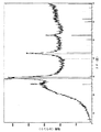
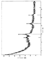
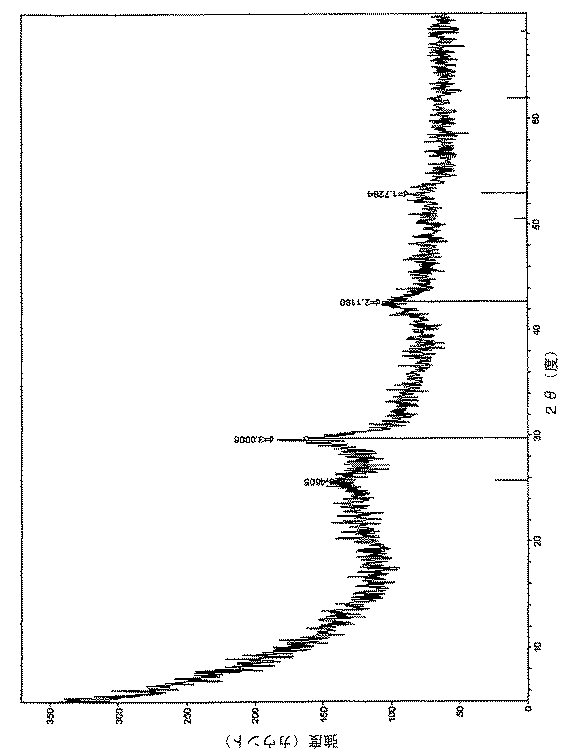
【解決手段】相変化記憶非晶性材料からなる薄膜をパルス・レーザ堆積により基板上に堆積し、相変化記憶非晶性材料を六方晶結晶相に転化させる、各工程を有する。相変化記憶非晶性材料は、原子パーセントで表して、5から45のGe、5から40のAs、またはAsの原子パーセントがSbの原子パーセントよりも大きいAsとSbの組合せ、45から65のTe、および、Al,Si,Ga,Se,In,Sn,Tl,Pb,Bi,P,S,またはそれらの組合せを含む。
【選択図】図1
Description
5から45のGe、
5から40のAs、またはAsとSbの組合せ、ここで、Asの原子パーセントはSbの原子パーセントよりも大きい、および
45から65のTe、
を含む。
10から30のGe、
15から30のAs、またはAsとSbの組合せ、ここで、Asの原子パーセントはSbの原子パーセントよりも大きい、および
50から60のTe、
を含む。
5から45のGe、
5から40のAs、またはAsとSbの組合せ、ここで、Asの原子パーセントはSbの原子パーセントよりも大きい、および
45から65のTe、
を含む。
10から30のGe、
15から30のAs、またはAsとSbの組合せ、ここで、Asの原子パーセントはSbの原子パーセントよりも大きい、および
50から60のTe、
を含む。
5から45のGe、
5から40のAs、またはAsとSbの組合せ、ここで、Asの原子パーセントはSbの原子パーセントよりも大きい、および
45から65のTe、
を含む。
10から30のGe、
15から30のAs、またはAsとSbの組合せ、ここで、Asの原子パーセントはSbの原子パーセントよりも大きい、および
50から60のTe、
を含む。
a. 少なくとも1つの六方晶結晶相を有する組成物からなる結晶化薄膜、または
b. 結晶化形態で少なくとも1つの六方晶相を有することのできる結晶化可能な組成物、
を備えた物品であって、
前記組成物が、原子パーセントで表して、
5から45のGe、
5から40のAs、またはAsとSbの組合せ、ここで、Asの原子パーセントはSbの原子パーセントよりも大きい、
45から65のTe、および
Al,Si,Ga,Se,In,Sn,Tl,Pb,Bi,P,S,またはそれらの組合せを含むものである、物品。
前記Al,Si,Ga,Se,In,Sn,Tl,Pb,Bi,P,S,またはそれらの組合せの原子パーセントが20パーセント以下であることを特徴とする実施態様1記載の物品。
前記薄膜が基板上に配置されることを特徴とする実施態様1または2記載の物品。
Claims (2)
- パルス・レーザ堆積により、相変化記憶非晶性材料からなる薄膜を基板上に堆積し、
該相変化記憶非晶性材料を六方晶結晶相に転化させる、
各工程を有してなり、
前記相変化記憶非晶性材料は、原子パーセントで表して、
5から45のGe、
5から40のAs、またはAsとSbの組合せ、ここで、Asの原子パーセントはSbの原子パーセントよりも大きい、
45から65のTe、および
Al,Si,Ga,Se,In,Sn,Tl,Pb,Bi,P,S,またはそれらの組合せを含むものである、
方法。 - パルス・レーザ堆積により、六方晶結晶相を有する相変化記憶材料からなる薄膜を基板上に堆積し、
該六方晶結晶相を非晶相に転化させる、
各工程を有してなり、
前記相変化記憶材料は、原子パーセントで表して、
5から45のGe、
5から40のAs、またはAsとSbの組合せ、ここで、Asの原子パーセントはSbの原子パーセントよりも大きい、
45から65のTe、および
Al,Si,Ga,Se,In,Sn,Tl,Pb,Bi,P,S,またはそれらの組合せを含むものである、
方法。
Applications Claiming Priority (4)
| Application Number | Priority Date | Filing Date | Title |
|---|---|---|---|
| US9286808P | 2008-08-29 | 2008-08-29 | |
| US61/092,868 | 2008-08-29 | ||
| US12/503,156 US8206804B2 (en) | 2008-08-29 | 2009-07-15 | Phase change memory materials |
| US12/503,156 | 2009-07-15 |
Related Parent Applications (1)
| Application Number | Title | Priority Date | Filing Date |
|---|---|---|---|
| JP2011525009A Division JP2012501511A (ja) | 2008-08-29 | 2009-08-28 | 相変化記憶材料 |
Publications (2)
| Publication Number | Publication Date |
|---|---|
| JP2015018596A true JP2015018596A (ja) | 2015-01-29 |
| JP6053041B2 JP6053041B2 (ja) | 2016-12-27 |
Family
ID=41507809
Family Applications (2)
| Application Number | Title | Priority Date | Filing Date |
|---|---|---|---|
| JP2011525009A Pending JP2012501511A (ja) | 2008-08-29 | 2009-08-28 | 相変化記憶材料 |
| JP2014146705A Expired - Fee Related JP6053041B2 (ja) | 2008-08-29 | 2014-07-17 | 相変化記憶材料 |
Family Applications Before (1)
| Application Number | Title | Priority Date | Filing Date |
|---|---|---|---|
| JP2011525009A Pending JP2012501511A (ja) | 2008-08-29 | 2009-08-28 | 相変化記憶材料 |
Country Status (7)
| Country | Link |
|---|---|
| US (1) | US8206804B2 (ja) |
| EP (1) | EP2335297A1 (ja) |
| JP (2) | JP2012501511A (ja) |
| KR (1) | KR101715956B1 (ja) |
| CN (1) | CN102138233B (ja) |
| TW (1) | TWI404633B (ja) |
| WO (1) | WO2010024936A1 (ja) |
Families Citing this family (4)
| Publication number | Priority date | Publication date | Assignee | Title |
|---|---|---|---|---|
| US10889887B2 (en) | 2016-08-22 | 2021-01-12 | Honeywell International Inc. | Chalcogenide sputtering target and method of making the same |
| CN106601907B (zh) * | 2016-12-14 | 2019-02-22 | 中国科学院上海微系统与信息技术研究所 | 一种选通管材料、选通管单元及其制作方法 |
| CN109880451B (zh) * | 2019-01-18 | 2020-12-18 | 申再军 | 基于相变的陶瓷包覆材料、墙体保温材料及其制备方法 |
| CN114400285B (zh) * | 2022-01-15 | 2025-12-19 | 西安交通大学 | 一种基于砷碲化合物的光学相变存储材料、器件及其制备方法 |
Citations (3)
| Publication number | Priority date | Publication date | Assignee | Title |
|---|---|---|---|---|
| WO1991005342A1 (en) * | 1989-09-28 | 1991-04-18 | Matsushita Electric Industrial Co., Ltd. | Optical data recording medium and method of producing the same |
| JPH0562239A (ja) * | 1991-06-20 | 1993-03-12 | Hitachi Ltd | 記録媒体及びこれを用いた情報の記録方法 |
| JP2008103053A (ja) * | 2006-03-13 | 2008-05-01 | Ricoh Co Ltd | 光記録媒体 |
Family Cites Families (10)
| Publication number | Priority date | Publication date | Assignee | Title |
|---|---|---|---|---|
| EP1372146B1 (en) * | 1999-05-19 | 2007-11-14 | Mitsubishi Kagaku Media Co., Ltd. | Optical recording method and medium. |
| JP2003200665A (ja) * | 2001-03-08 | 2003-07-15 | Mitsubishi Chemicals Corp | 光学的情報記録用媒体及びその記録消去方法並びに製造方法 |
| US20020160305A1 (en) * | 2001-03-08 | 2002-10-31 | Mitsubishi Chemical Corporation | Optical recording medium, method of writing and erasing information using the same, and process of producing the same |
| US6930913B2 (en) | 2002-02-20 | 2005-08-16 | Stmicroelectronics S.R.L. | Contact structure, phase change memory cell, and manufacturing method thereof with elimination of double contacts |
| TWI226058B (en) * | 2002-09-11 | 2005-01-01 | Tdk Corp | Optical recording medium |
| KR100651657B1 (ko) * | 2005-06-29 | 2006-12-01 | 한국과학기술연구원 | 고집적 비휘발성 메모리용 상변화 재료 |
| US8188454B2 (en) * | 2005-10-28 | 2012-05-29 | Ovonyx, Inc. | Forming a phase change memory with an ovonic threshold switch |
| US7626190B2 (en) * | 2006-06-02 | 2009-12-01 | Infineon Technologies Ag | Memory device, in particular phase change random access memory device with transistor, and method for fabricating a memory device |
| KR20080055508A (ko) * | 2006-12-15 | 2008-06-19 | 삼성전자주식회사 | 한 층에서 다른 결정 격자 구조를 갖는 상변화층 및 그형성 방법과 Ti 확산 방지 수단을 구비하는 상변화메모리 소자 및 그 제조 방법 |
| KR20090002506A (ko) * | 2007-06-29 | 2009-01-09 | 제일모직주식회사 | 상변화 메모리 소자 연마용 cmp 슬러리 조성물 및 이를이용한 연마 방법 |
-
2009
- 2009-07-15 US US12/503,156 patent/US8206804B2/en not_active Expired - Fee Related
- 2009-08-28 KR KR1020117007093A patent/KR101715956B1/ko not_active Expired - Fee Related
- 2009-08-28 JP JP2011525009A patent/JP2012501511A/ja active Pending
- 2009-08-28 EP EP09789238A patent/EP2335297A1/en not_active Withdrawn
- 2009-08-28 CN CN200980134692.6A patent/CN102138233B/zh not_active Expired - Fee Related
- 2009-08-28 TW TW98129195A patent/TWI404633B/zh not_active IP Right Cessation
- 2009-08-28 WO PCT/US2009/004922 patent/WO2010024936A1/en not_active Ceased
-
2014
- 2014-07-17 JP JP2014146705A patent/JP6053041B2/ja not_active Expired - Fee Related
Patent Citations (3)
| Publication number | Priority date | Publication date | Assignee | Title |
|---|---|---|---|---|
| WO1991005342A1 (en) * | 1989-09-28 | 1991-04-18 | Matsushita Electric Industrial Co., Ltd. | Optical data recording medium and method of producing the same |
| JPH0562239A (ja) * | 1991-06-20 | 1993-03-12 | Hitachi Ltd | 記録媒体及びこれを用いた情報の記録方法 |
| JP2008103053A (ja) * | 2006-03-13 | 2008-05-01 | Ricoh Co Ltd | 光記録媒体 |
Non-Patent Citations (1)
| Title |
|---|
| JPN5011012568; MOHAMED S H: 'STRUCTURAL AND OPTICAL PROPERTIES OF GE-AS-TE THIN FILMS' EUROPEAN PHYSICAL JOURNAL V34 N3, 200606, P165-171, APPLIED PHYSICS EDP SCIENCES * |
Also Published As
| Publication number | Publication date |
|---|---|
| TW201026504A (en) | 2010-07-16 |
| TWI404633B (zh) | 2013-08-11 |
| US20100055493A1 (en) | 2010-03-04 |
| KR101715956B1 (ko) | 2017-03-13 |
| CN102138233B (zh) | 2014-07-02 |
| JP2012501511A (ja) | 2012-01-19 |
| CN102138233A (zh) | 2011-07-27 |
| EP2335297A1 (en) | 2011-06-22 |
| US8206804B2 (en) | 2012-06-26 |
| WO2010024936A1 (en) | 2010-03-04 |
| JP6053041B2 (ja) | 2016-12-27 |
| KR20110059732A (ko) | 2011-06-03 |
Similar Documents
| Publication | Publication Date | Title |
|---|---|---|
| EP0499273B1 (en) | Congruent state changeable optical memory alloy and data carrier | |
| US6723410B2 (en) | Optical recording medium | |
| Buller et al. | Influence of partial substitution of Te by Se and Ge by Sn on the properties of the Blu-ray phase-change material Ge8Sb2Te11 | |
| JP6053041B2 (ja) | 相変化記憶材料 | |
| TW487682B (en) | Rewritable phase-change type optical information recording composition and optical disk containing the same | |
| CN104868053B (zh) | 一种用于相变存储器的Ge‑Sb‑Te‑Se薄膜材料及其制备方法 | |
| Lie et al. | Ge2Sb2Te5 thin film doped with silver | |
| WO2023008432A1 (ja) | 相変化材料 | |
| JP3899770B2 (ja) | 光学的情報記録用媒体並びにその再生方法及び記録方法 | |
| Yamada | Development of materials for third generation optical storage media | |
| TW479257B (en) | Rewritable optical information medium | |
| KR20080016120A (ko) | 상변화 메모리 소자 및 이의 제조방법 | |
| Choi et al. | Growth and Phase Separation Behavior in Ge-Doped Sb− Te Thin Films Deposited by Combined Plasma-Enhanced Chemical Vapor and Atomic Layer Depositions | |
| CN111725397A (zh) | 一种相变材料结构、存储器单元及其制作方法 | |
| JP7687722B2 (ja) | 相変化材料および相変化型メモリ素子 | |
| CN1291401C (zh) | 可重写型光学信息记录媒体及其记录方法 | |
| KR100411336B1 (ko) | 되쓰기형 광기록매체용 상변화형 광기록재료 | |
| CN101371305B (zh) | 光学记录介质 | |
| US6753059B2 (en) | Optical recording material and optical recording medium using same | |
| Lee et al. | Ultra-high-density phase-change storage using AlNiGd metallic glass thin film as recording layer | |
| TW554339B (en) | Optical information recording medium | |
| Mongia et al. | Crystallization kinetics in (AgSbTe) x (In1− ySby) 1− x films used in optical data storage | |
| CN116583166A (zh) | 一种可用于相变存储器件的新型相变薄膜材料与制备方法 | |
| Zhu et al. | Research on phase-change of disc recording media GaSbBi | |
| Jones | Phase change memory materials: Why do Ge/Sb/Te alloys dominate |
Legal Events
| Date | Code | Title | Description |
|---|---|---|---|
| A977 | Report on retrieval |
Free format text: JAPANESE INTERMEDIATE CODE: A971007 Effective date: 20151119 |
|
| A131 | Notification of reasons for refusal |
Free format text: JAPANESE INTERMEDIATE CODE: A131 Effective date: 20151124 |
|
| A601 | Written request for extension of time |
Free format text: JAPANESE INTERMEDIATE CODE: A601 Effective date: 20160222 |
|
| A601 | Written request for extension of time |
Free format text: JAPANESE INTERMEDIATE CODE: A601 Effective date: 20160311 |
|
| A521 | Request for written amendment filed |
Free format text: JAPANESE INTERMEDIATE CODE: A523 Effective date: 20160511 |
|
| TRDD | Decision of grant or rejection written | ||
| A01 | Written decision to grant a patent or to grant a registration (utility model) |
Free format text: JAPANESE INTERMEDIATE CODE: A01 Effective date: 20161101 |
|
| A61 | First payment of annual fees (during grant procedure) |
Free format text: JAPANESE INTERMEDIATE CODE: A61 Effective date: 20161125 |
|
| R150 | Certificate of patent or registration of utility model |
Ref document number: 6053041 Country of ref document: JP Free format text: JAPANESE INTERMEDIATE CODE: R150 |
|
| LAPS | Cancellation because of no payment of annual fees |