JP2015019070A - p型ガリウムナイトライド電流障壁層を有する垂直型トランジスタおよびその製造方法 - Google Patents
p型ガリウムナイトライド電流障壁層を有する垂直型トランジスタおよびその製造方法 Download PDFInfo
- Publication number
- JP2015019070A JP2015019070A JP2014142115A JP2014142115A JP2015019070A JP 2015019070 A JP2015019070 A JP 2015019070A JP 2014142115 A JP2014142115 A JP 2014142115A JP 2014142115 A JP2014142115 A JP 2014142115A JP 2015019070 A JP2015019070 A JP 2015019070A
- Authority
- JP
- Japan
- Prior art keywords
- layer
- gallium nitride
- gan
- type gallium
- current barrier
- Prior art date
- Legal status (The legal status is an assumption and is not a legal conclusion. Google has not performed a legal analysis and makes no representation as to the accuracy of the status listed.)
- Granted
Links
Images








Classifications
-
- H—ELECTRICITY
- H10—SEMICONDUCTOR DEVICES; ELECTRIC SOLID-STATE DEVICES NOT OTHERWISE PROVIDED FOR
- H10P—GENERIC PROCESSES OR APPARATUS FOR THE MANUFACTURE OR TREATMENT OF DEVICES COVERED BY CLASS H10
- H10P10/00—Bonding of wafers, substrates or parts of devices
-
- H—ELECTRICITY
- H10—SEMICONDUCTOR DEVICES; ELECTRIC SOLID-STATE DEVICES NOT OTHERWISE PROVIDED FOR
- H10D—INORGANIC ELECTRIC SEMICONDUCTOR DEVICES
- H10D30/00—Field-effect transistors [FET]
- H10D30/01—Manufacture or treatment
- H10D30/015—Manufacture or treatment of FETs having heterojunction interface channels or heterojunction gate electrodes, e.g. HEMT
-
- H—ELECTRICITY
- H10—SEMICONDUCTOR DEVICES; ELECTRIC SOLID-STATE DEVICES NOT OTHERWISE PROVIDED FOR
- H10D—INORGANIC ELECTRIC SEMICONDUCTOR DEVICES
- H10D30/00—Field-effect transistors [FET]
- H10D30/01—Manufacture or treatment
- H10D30/021—Manufacture or treatment of FETs having insulated gates [IGFET]
- H10D30/028—Manufacture or treatment of FETs having insulated gates [IGFET] of double-diffused metal oxide semiconductor [DMOS] FETs
- H10D30/0291—Manufacture or treatment of FETs having insulated gates [IGFET] of double-diffused metal oxide semiconductor [DMOS] FETs of vertical DMOS [VDMOS] FETs
- H10D30/0295—Manufacture or treatment of FETs having insulated gates [IGFET] of double-diffused metal oxide semiconductor [DMOS] FETs of vertical DMOS [VDMOS] FETs using recessing of the source electrodes
-
- H—ELECTRICITY
- H10—SEMICONDUCTOR DEVICES; ELECTRIC SOLID-STATE DEVICES NOT OTHERWISE PROVIDED FOR
- H10D—INORGANIC ELECTRIC SEMICONDUCTOR DEVICES
- H10D30/00—Field-effect transistors [FET]
- H10D30/40—FETs having zero-dimensional [0D], one-dimensional [1D] or two-dimensional [2D] charge carrier gas channels
- H10D30/47—FETs having zero-dimensional [0D], one-dimensional [1D] or two-dimensional [2D] charge carrier gas channels having two-dimensional [2D] charge carrier gas channels, e.g. nanoribbon FETs or high electron mobility transistors [HEMT]
-
- H—ELECTRICITY
- H10—SEMICONDUCTOR DEVICES; ELECTRIC SOLID-STATE DEVICES NOT OTHERWISE PROVIDED FOR
- H10D—INORGANIC ELECTRIC SEMICONDUCTOR DEVICES
- H10D30/00—Field-effect transistors [FET]
- H10D30/40—FETs having zero-dimensional [0D], one-dimensional [1D] or two-dimensional [2D] charge carrier gas channels
- H10D30/47—FETs having zero-dimensional [0D], one-dimensional [1D] or two-dimensional [2D] charge carrier gas channels having two-dimensional [2D] charge carrier gas channels, e.g. nanoribbon FETs or high electron mobility transistors [HEMT]
- H10D30/471—High electron mobility transistors [HEMT] or high hole mobility transistors [HHMT]
- H10D30/477—Vertical HEMTs or vertical HHMTs
-
- H—ELECTRICITY
- H10—SEMICONDUCTOR DEVICES; ELECTRIC SOLID-STATE DEVICES NOT OTHERWISE PROVIDED FOR
- H10D—INORGANIC ELECTRIC SEMICONDUCTOR DEVICES
- H10D30/00—Field-effect transistors [FET]
- H10D30/60—Insulated-gate field-effect transistors [IGFET]
- H10D30/64—Double-diffused metal-oxide semiconductor [DMOS] FETs
- H10D30/66—Vertical DMOS [VDMOS] FETs
-
- H—ELECTRICITY
- H10—SEMICONDUCTOR DEVICES; ELECTRIC SOLID-STATE DEVICES NOT OTHERWISE PROVIDED FOR
- H10D—INORGANIC ELECTRIC SEMICONDUCTOR DEVICES
- H10D30/00—Field-effect transistors [FET]
- H10D30/60—Insulated-gate field-effect transistors [IGFET]
- H10D30/64—Double-diffused metal-oxide semiconductor [DMOS] FETs
- H10D30/66—Vertical DMOS [VDMOS] FETs
- H10D30/668—Vertical DMOS [VDMOS] FETs having trench gate electrodes, e.g. UMOS transistors
-
- H—ELECTRICITY
- H10—SEMICONDUCTOR DEVICES; ELECTRIC SOLID-STATE DEVICES NOT OTHERWISE PROVIDED FOR
- H10D—INORGANIC ELECTRIC SEMICONDUCTOR DEVICES
- H10D62/00—Semiconductor bodies, or regions thereof, of devices having potential barriers
- H10D62/10—Shapes, relative sizes or dispositions of the regions of the semiconductor bodies; Shapes of the semiconductor bodies
- H10D62/102—Constructional design considerations for preventing surface leakage or controlling electric field concentration
- H10D62/103—Constructional design considerations for preventing surface leakage or controlling electric field concentration for increasing or controlling the breakdown voltage of reverse-biased devices
- H10D62/105—Constructional design considerations for preventing surface leakage or controlling electric field concentration for increasing or controlling the breakdown voltage of reverse-biased devices by having particular doping profiles, shapes or arrangements of PN junctions; by having supplementary regions, e.g. junction termination extension [JTE]
- H10D62/106—Constructional design considerations for preventing surface leakage or controlling electric field concentration for increasing or controlling the breakdown voltage of reverse-biased devices by having particular doping profiles, shapes or arrangements of PN junctions; by having supplementary regions, e.g. junction termination extension [JTE] having supplementary regions doped oppositely to or in rectifying contact with regions of the semiconductor bodies, e.g. guard rings with PN or Schottky junctions
- H10D62/107—Buried supplementary regions, e.g. buried guard rings
-
- H—ELECTRICITY
- H10—SEMICONDUCTOR DEVICES; ELECTRIC SOLID-STATE DEVICES NOT OTHERWISE PROVIDED FOR
- H10D—INORGANIC ELECTRIC SEMICONDUCTOR DEVICES
- H10D62/00—Semiconductor bodies, or regions thereof, of devices having potential barriers
- H10D62/10—Shapes, relative sizes or dispositions of the regions of the semiconductor bodies; Shapes of the semiconductor bodies
- H10D62/113—Isolations within a component, i.e. internal isolations
- H10D62/115—Dielectric isolations, e.g. air gaps
- H10D62/116—Dielectric isolations, e.g. air gaps adjoining the input or output regions of field-effect devices, e.g. adjoining source or drain regions
-
- H—ELECTRICITY
- H10—SEMICONDUCTOR DEVICES; ELECTRIC SOLID-STATE DEVICES NOT OTHERWISE PROVIDED FOR
- H10D—INORGANIC ELECTRIC SEMICONDUCTOR DEVICES
- H10D62/00—Semiconductor bodies, or regions thereof, of devices having potential barriers
- H10D62/80—Semiconductor bodies, or regions thereof, of devices having potential barriers characterised by the materials
- H10D62/85—Semiconductor bodies, or regions thereof, of devices having potential barriers characterised by the materials being Group III-V materials, e.g. GaAs
- H10D62/8503—Nitride Group III-V materials, e.g. AlN or GaN
-
- H—ELECTRICITY
- H10—SEMICONDUCTOR DEVICES; ELECTRIC SOLID-STATE DEVICES NOT OTHERWISE PROVIDED FOR
- H10D—INORGANIC ELECTRIC SEMICONDUCTOR DEVICES
- H10D64/00—Electrodes of devices having potential barriers
- H10D64/20—Electrodes characterised by their shapes, relative sizes or dispositions
- H10D64/23—Electrodes carrying the current to be rectified, amplified, oscillated or switched, e.g. sources, drains, anodes or cathodes
- H10D64/251—Source or drain electrodes for field-effect devices
- H10D64/252—Source or drain electrodes for field-effect devices for vertical or pseudo-vertical devices
-
- H—ELECTRICITY
- H10—SEMICONDUCTOR DEVICES; ELECTRIC SOLID-STATE DEVICES NOT OTHERWISE PROVIDED FOR
- H10D—INORGANIC ELECTRIC SEMICONDUCTOR DEVICES
- H10D64/00—Electrodes of devices having potential barriers
- H10D64/20—Electrodes characterised by their shapes, relative sizes or dispositions
- H10D64/23—Electrodes carrying the current to be rectified, amplified, oscillated or switched, e.g. sources, drains, anodes or cathodes
- H10D64/251—Source or drain electrodes for field-effect devices
- H10D64/256—Source or drain electrodes for field-effect devices for lateral devices wherein the source or drain electrodes are recessed in semiconductor bodies
-
- H—ELECTRICITY
- H10—SEMICONDUCTOR DEVICES; ELECTRIC SOLID-STATE DEVICES NOT OTHERWISE PROVIDED FOR
- H10P—GENERIC PROCESSES OR APPARATUS FOR THE MANUFACTURE OR TREATMENT OF DEVICES COVERED BY CLASS H10
- H10P72/00—Handling or holding of wafers, substrates or devices during manufacture or treatment thereof
- H10P72/70—Handling or holding of wafers, substrates or devices during manufacture or treatment thereof for supporting or gripping
- H10P72/74—Handling or holding of wafers, substrates or devices during manufacture or treatment thereof for supporting or gripping using temporarily an auxiliary support
-
- H—ELECTRICITY
- H10—SEMICONDUCTOR DEVICES; ELECTRIC SOLID-STATE DEVICES NOT OTHERWISE PROVIDED FOR
- H10D—INORGANIC ELECTRIC SEMICONDUCTOR DEVICES
- H10D62/00—Semiconductor bodies, or regions thereof, of devices having potential barriers
- H10D62/10—Shapes, relative sizes or dispositions of the regions of the semiconductor bodies; Shapes of the semiconductor bodies
- H10D62/13—Semiconductor regions connected to electrodes carrying current to be rectified, amplified or switched, e.g. source or drain regions
- H10D62/149—Source or drain regions of field-effect devices
- H10D62/151—Source or drain regions of field-effect devices of IGFETs
- H10D62/156—Drain regions of DMOS transistors
- H10D62/157—Impurity concentrations or distributions
-
- H—ELECTRICITY
- H10—SEMICONDUCTOR DEVICES; ELECTRIC SOLID-STATE DEVICES NOT OTHERWISE PROVIDED FOR
- H10P—GENERIC PROCESSES OR APPARATUS FOR THE MANUFACTURE OR TREATMENT OF DEVICES COVERED BY CLASS H10
- H10P34/00—Irradiation with electromagnetic or particle radiation of wafers, substrates or parts of devices
- H10P34/40—Irradiation with electromagnetic or particle radiation of wafers, substrates or parts of devices with high-energy radiation
- H10P34/42—Irradiation with electromagnetic or particle radiation of wafers, substrates or parts of devices with high-energy radiation with electromagnetic radiation, e.g. laser annealing
-
- H—ELECTRICITY
- H10—SEMICONDUCTOR DEVICES; ELECTRIC SOLID-STATE DEVICES NOT OTHERWISE PROVIDED FOR
- H10P—GENERIC PROCESSES OR APPARATUS FOR THE MANUFACTURE OR TREATMENT OF DEVICES COVERED BY CLASS H10
- H10P72/00—Handling or holding of wafers, substrates or devices during manufacture or treatment thereof
- H10P72/70—Handling or holding of wafers, substrates or devices during manufacture or treatment thereof for supporting or gripping
- H10P72/74—Handling or holding of wafers, substrates or devices during manufacture or treatment thereof for supporting or gripping using temporarily an auxiliary support
- H10P72/7412—Handling or holding of wafers, substrates or devices during manufacture or treatment thereof for supporting or gripping using temporarily an auxiliary support the auxiliary support including means facilitating the separation of a device or wafer from the auxiliary support
-
- H—ELECTRICITY
- H10—SEMICONDUCTOR DEVICES; ELECTRIC SOLID-STATE DEVICES NOT OTHERWISE PROVIDED FOR
- H10P—GENERIC PROCESSES OR APPARATUS FOR THE MANUFACTURE OR TREATMENT OF DEVICES COVERED BY CLASS H10
- H10P72/00—Handling or holding of wafers, substrates or devices during manufacture or treatment thereof
- H10P72/70—Handling or holding of wafers, substrates or devices during manufacture or treatment thereof for supporting or gripping
- H10P72/74—Handling or holding of wafers, substrates or devices during manufacture or treatment thereof for supporting or gripping using temporarily an auxiliary support
- H10P72/7426—Handling or holding of wafers, substrates or devices during manufacture or treatment thereof for supporting or gripping using temporarily an auxiliary support used as a support during build up manufacturing of active devices
-
- H—ELECTRICITY
- H10—SEMICONDUCTOR DEVICES; ELECTRIC SOLID-STATE DEVICES NOT OTHERWISE PROVIDED FOR
- H10P—GENERIC PROCESSES OR APPARATUS FOR THE MANUFACTURE OR TREATMENT OF DEVICES COVERED BY CLASS H10
- H10P72/00—Handling or holding of wafers, substrates or devices during manufacture or treatment thereof
- H10P72/70—Handling or holding of wafers, substrates or devices during manufacture or treatment thereof for supporting or gripping
- H10P72/74—Handling or holding of wafers, substrates or devices during manufacture or treatment thereof for supporting or gripping using temporarily an auxiliary support
- H10P72/7432—Handling or holding of wafers, substrates or devices during manufacture or treatment thereof for supporting or gripping using temporarily an auxiliary support used in a transfer process involving transfer directly from an origin substrate to a target substrate without use of an intermediate handle substrate
-
- H—ELECTRICITY
- H10—SEMICONDUCTOR DEVICES; ELECTRIC SOLID-STATE DEVICES NOT OTHERWISE PROVIDED FOR
- H10P—GENERIC PROCESSES OR APPARATUS FOR THE MANUFACTURE OR TREATMENT OF DEVICES COVERED BY CLASS H10
- H10P72/00—Handling or holding of wafers, substrates or devices during manufacture or treatment thereof
- H10P72/70—Handling or holding of wafers, substrates or devices during manufacture or treatment thereof for supporting or gripping
- H10P72/74—Handling or holding of wafers, substrates or devices during manufacture or treatment thereof for supporting or gripping using temporarily an auxiliary support
- H10P72/744—Details of chemical or physical process used for separating the auxiliary support from a device or a wafer
Landscapes
- Junction Field-Effect Transistors (AREA)
- Electrodes Of Semiconductors (AREA)
- Thin Film Transistor (AREA)
Abstract
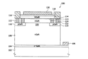
【解決手段】基板102の第1領域上のドレイン電極106と、基板102における、第1領域と離隔した第2領域上のドリフト層108と、ドリフト層108の上部に配置され、電流アパーチャ109を構成するp型GaN電流障壁層110と、p型GaN電流障壁層110およびドリフト層108の上に配置されるチャネル層112と、チャネル層112上に配置され、チャネル層の表面に隣接する2次元電子ガス層113の形成を引き起こす半導体層114と、チャネル層112内に配置され、p型GaN電流障壁層110とコンタクトする金属コンタクトプラグ124と、金属コンタクトプラグ124およびチャネル層112上のソース電極116と、半導体層114の上部面上に順に積層されたゲート絶縁層118およびゲート電極層120とを含む。
【選択図】図2
Description
Claims (22)
- 基板の第1領域上のドレイン電極と、
前記基板における、前記第1領域と離隔した第2領域上のドリフト層と、
前記ドリフト層の上部に配置されたp型ガリウムナイトライド(GaN)電流障壁層であって、それらの間に電流アパーチャを構成し、前記電流アパーチャが、垂直方向にキャリアが移動する経路を提供する、p型ガリウムナイトライド(GaN)電流障壁層と、
前記p型ガリウムナイトライド(GaN)電流障壁層およびドリフト層の上に配置され、その表面に隣接して2次元電子ガス層を有するチャネル層と、
前記チャネル層上に配置され、前記2次元電子ガス層の形成を引き起こす半導体層と、
前記チャネル層内に配置され、前記p型ガリウムナイトライド(GaN)電流障壁層とコンタクトする金属コンタクトプラグと、
前記金属コンタクトプラグおよび前記チャネル層上のソース電極と、
前記チャネル層の反対側である前記半導体層の上部面上に順に積層されたゲート絶縁層およびゲート電極とを含む、垂直型トランジスタ。 - 前記ドリフト層は、n型ガリウムナイトライド(GaN)層を含む、請求項1に記載の垂直型トランジスタ。
- 前記チャネル層は、ガリウムナイトライド(GaN)層を含み、前記半導体層は、アルミニウムガリウムナイトライド(AlGaN)層を含む、請求項1に記載の垂直型トランジスタ。
- 前記金属コンタクトプラグは、平面視で円形形状を有する、請求項1に記載の垂直型トランジスタ。
- 前記金属コンタクトプラグは、平面視で矩形形状を有する、請求項1に記載の垂直型トランジスタ。
- 隣接する前記金属コンタクトプラグ間の距離は、5μm以下である、請求項1に記載の垂直型トランジスタ。
- ドレイン電極上のドリフト層と、
前記ドリフト層の上部に配置されるp型ガリウムナイトライド(GaN)電流障壁層と、
前記p型ガリウムナイトライド(GaN)電流障壁層上に配置されるドナー層と、
前記ドナー層内に配置され、前記p型ガリウムナイトライド(GaN)電流障壁層とコンタクトする金属コンタクトプラグと、
前記金属コンタクトプラグおよびドナー層上のソース電極と、
前記ドナー層、前記p型ガリウムナイトライド(GaN)電流障壁層および前記ドリフト層内に形成されるトレンチと、
前記トレンチの内壁に配置されたゲート絶縁層と、
前記ゲート絶縁層上に配置されるゲート電極とを含む、垂直型トランジスタ。 - 前記ドレイン電極と前記ドリフト層との間に配置される基板と、
前記基板と前記ドリフト層との間に配置されるバッファ層をさらに含む、請求項7に記載の垂直型トランジスタ。 - 前記ドリフト層は、n型ガリウムナイトライド(GaN)層を含み、前記ドナー層は、n+型ガリウムナイトライド(GaN)層を含む、請求項7に記載の垂直型トランジスタ。
- 前記金属コンタクトプラグは、平面視で円形形状を有する、請求項7に記載の垂直型トランジスタ。
- 前記金属コンタクトプラグは、平面視で矩形形状を有する、請求項7に記載の垂直型トランジスタ。
- 前記金属コンタクトプラグ間の距離は、5μm以下である、請求項7に記載の垂直型トランジスタ。
- ドレイン電極と、
前記ドレイン電極の上部に配置され、電流流れ経路(current flow path)を提供する開口部によって分離される電流遮断パターンと、
前記開口部において前記ドレイン電極上に配置される低抵抗パターンと、
前記低抵抗パターンおよび前記電流遮断パターンを覆うドリフト層と、
前記ドリフト層内に配置され、その表面にチャネル領域を有するp型ガリウムナイトライド(GaN)電流障壁層と、
前記p型ガリウムナイトライド(GaN)電流障壁層の上部に配置されるドナー層と、
前記ドナー層内に配置され、前記p型ガリウムナイトライド(GaN)電流障壁層とコンタクトする金属コンタクトプラグと、
前記金属コンタクトプラグおよび前記ドナー層上のソース電極と、
前記p型ガリウムナイトライド(GaN)電流障壁層の間の前記ドリフト層上に配置されるゲート絶縁層と、
前記ゲート絶縁層上に配置されるゲート電極とを含み、
前記ゲート絶縁層および前記ゲート電極が、前記p型ガリウムナイトライド(GaN)電流障壁層の前記チャネル領域上まで延長されている、垂直型トランジスタ。 - 前記低抵抗パターンは、n+型ガリウムナイトライド(GaN)層を含み、前記ドリフト層は、前記低抵抗パターンよりも不純物濃度の低いn型ガリウムナイトライド(GaN)層を含み、前記ドナー層は、前記ドリフト層よりも不純物濃度の高いn+型ガリウムナイトライド(GaN)層を含む、請求項13に記載の垂直型トランジスタ。
- 前記金属コンタクトプラグは、円形形状を有する、請求項13に記載の垂直型トランジスタ。
- 前記金属コンタクトプラグは、矩形形状を有する、請求項13に記載の垂直型トランジスタ。
- 前記金属コンタクトプラグ間の距離は、5μm以下である、請求項13に記載の垂直型トランジスタ。
- ドレイン電極と、前記ドレイン電極上のドリフト層と、前記ドリフト層上のp型ガリウムナイトライド(GaN)電流障壁層と、前記p型ガリウムナイトライド(GaN)電流障壁層上のドナー層とを形成するステップと、
前記ドナー層をパターニングして前記p型ガリウムナイトライド(GaN)電流障壁層の一部表面を露出させるホールを形成するステップと、
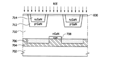
前記ホールを形成した後、前記p型ガリウムナイトライド(GaN)電流障壁層内の水素成分を除去するステップとを含む、垂直型トランジスタの製造方法。 - 前記ホールは、平面視で円形形状である、請求項18に記載の垂直型トランジスタの製造方法。
- 前記ホールは、平面視で矩形形状である、請求項18に記載の垂直型トランジスタの製造方法。
- 前記p型ガリウムナイトライド(GaN)電流障壁層内の水素成分を除去するステップは、前記ホールによって露出するp型ガリウムナイトライド(GaN)電流障壁層の露出表面に対してパルスレーザを照射して行うことを含む、請求項18に記載の垂直型トランジスタの製造方法。
- 前記ホールの内部を金属で満たすステップをさらに含む、請求項18に記載の垂直型トランジスタの製造方法。
Applications Claiming Priority (2)
| Application Number | Priority Date | Filing Date | Title |
|---|---|---|---|
| KR1020130081622A KR20150007546A (ko) | 2013-07-11 | 2013-07-11 | p형 갈륨나이트라이드 전류장벽층을 갖는 수직형 트랜지스터 및 그 제조방법 |
| KR10-2013-0081622 | 2013-07-11 |
Publications (2)
| Publication Number | Publication Date |
|---|---|
| JP2015019070A true JP2015019070A (ja) | 2015-01-29 |
| JP5805276B2 JP5805276B2 (ja) | 2015-11-04 |
Family
ID=51176196
Family Applications (1)
| Application Number | Title | Priority Date | Filing Date |
|---|---|---|---|
| JP2014142115A Active JP5805276B2 (ja) | 2013-07-11 | 2014-07-10 | p型ガリウムナイトライド電流障壁層を有する垂直型トランジスタおよびその製造方法 |
Country Status (5)
| Country | Link |
|---|---|
| US (1) | US20150014699A1 (ja) |
| EP (1) | EP2824711A3 (ja) |
| JP (1) | JP5805276B2 (ja) |
| KR (1) | KR20150007546A (ja) |
| CN (1) | CN104282746A (ja) |
Cited By (4)
| Publication number | Priority date | Publication date | Assignee | Title |
|---|---|---|---|---|
| JP2019087690A (ja) * | 2017-11-09 | 2019-06-06 | 株式会社豊田中央研究所 | 窒化物半導体装置とその製造方法 |
| JP2019087689A (ja) * | 2017-11-09 | 2019-06-06 | 株式会社豊田中央研究所 | 窒化物半導体装置とその製造方法 |
| JP2021114496A (ja) * | 2020-01-16 | 2021-08-05 | 信一郎 高谷 | 縦型窒化物半導体トランジスタ装置 |
| JP2024126913A (ja) * | 2023-03-08 | 2024-09-20 | 株式会社デンソー | 窒化物半導体装置とその製造方法 |
Families Citing this family (12)
| Publication number | Priority date | Publication date | Assignee | Title |
|---|---|---|---|---|
| CN105470294A (zh) * | 2015-12-08 | 2016-04-06 | 北京华进创威电子有限公司 | 一种垂直型氮化镓功率开关器件及其制备方法 |
| US10147813B2 (en) * | 2016-03-04 | 2018-12-04 | United Silicon Carbide, Inc. | Tunneling field effect transistor |
| CN109314138B (zh) * | 2016-10-28 | 2021-10-15 | 华为技术有限公司 | 场效应晶体管及其制造方法 |
| CN109952656B (zh) * | 2016-11-11 | 2021-11-05 | 住友电气工业株式会社 | 碳化硅半导体器件 |
| CN111886683B (zh) * | 2018-03-22 | 2024-01-02 | 松下控股株式会社 | 氮化物半导体装置 |
| CN111129139B (zh) * | 2018-11-01 | 2021-03-30 | 西安电子科技大学 | 一种基于悬浮场板的自对准栅氮化镓增强型垂直功率器件 |
| CN111584620A (zh) * | 2020-05-28 | 2020-08-25 | 西安电子科技大学芜湖研究院 | 一种降低p型mosfet源漏电极接触电阻的制备方法 |
| CN114078965B (zh) | 2020-08-11 | 2023-08-08 | 联华电子股份有限公司 | 高电子迁移率晶体管及其制作方法 |
| US11978790B2 (en) | 2020-12-01 | 2024-05-07 | Texas Instruments Incorporated | Normally-on gallium nitride based transistor with p-type gate |
| CN113030802B (zh) * | 2021-02-23 | 2023-05-16 | 南京邮电大学 | 一种基于类cavet晶体管结构的高灵敏度磁场传感器 |
| CN113539822B (zh) * | 2021-09-16 | 2022-01-28 | 浙江大学杭州国际科创中心 | 一种垂直电流孔径晶体管制备方法 |
| US20240055509A1 (en) * | 2021-12-31 | 2024-02-15 | Innoscience (Suzhou) Technology Co., Ltd. | Nitride-based semiconductor device and method for manufacturing the same |
Citations (3)
| Publication number | Priority date | Publication date | Assignee | Title |
|---|---|---|---|---|
| JP2004055869A (ja) * | 2002-07-22 | 2004-02-19 | Nec Corp | 半導体装置 |
| WO2012177699A1 (en) * | 2011-06-20 | 2012-12-27 | The Regents Of The University Of California | Current aperture vertical electron transistors |
| JPWO2011024549A1 (ja) * | 2009-08-31 | 2013-01-24 | 日本電気株式会社 | 半導体装置および電界効果トランジスタ |
Family Cites Families (2)
| Publication number | Priority date | Publication date | Assignee | Title |
|---|---|---|---|---|
| JP2009117820A (ja) * | 2007-10-16 | 2009-05-28 | Rohm Co Ltd | 窒化物半導体素子および窒化物半導体素子の製造方法 |
| JP4985760B2 (ja) * | 2009-12-28 | 2012-07-25 | 住友電気工業株式会社 | 半導体装置およびその製造方法 |
-
2013
- 2013-07-11 KR KR1020130081622A patent/KR20150007546A/ko not_active Ceased
-
2014
- 2014-07-09 CN CN201410325340.1A patent/CN104282746A/zh active Pending
- 2014-07-09 US US14/327,204 patent/US20150014699A1/en not_active Abandoned
- 2014-07-10 JP JP2014142115A patent/JP5805276B2/ja active Active
- 2014-07-10 EP EP14176590.9A patent/EP2824711A3/en not_active Withdrawn
Patent Citations (3)
| Publication number | Priority date | Publication date | Assignee | Title |
|---|---|---|---|---|
| JP2004055869A (ja) * | 2002-07-22 | 2004-02-19 | Nec Corp | 半導体装置 |
| JPWO2011024549A1 (ja) * | 2009-08-31 | 2013-01-24 | 日本電気株式会社 | 半導体装置および電界効果トランジスタ |
| WO2012177699A1 (en) * | 2011-06-20 | 2012-12-27 | The Regents Of The University Of California | Current aperture vertical electron transistors |
Cited By (5)
| Publication number | Priority date | Publication date | Assignee | Title |
|---|---|---|---|---|
| JP2019087690A (ja) * | 2017-11-09 | 2019-06-06 | 株式会社豊田中央研究所 | 窒化物半導体装置とその製造方法 |
| JP2019087689A (ja) * | 2017-11-09 | 2019-06-06 | 株式会社豊田中央研究所 | 窒化物半導体装置とその製造方法 |
| JP7031238B2 (ja) | 2017-11-09 | 2022-03-08 | 株式会社豊田中央研究所 | 窒化物半導体装置とその製造方法 |
| JP2021114496A (ja) * | 2020-01-16 | 2021-08-05 | 信一郎 高谷 | 縦型窒化物半導体トランジスタ装置 |
| JP2024126913A (ja) * | 2023-03-08 | 2024-09-20 | 株式会社デンソー | 窒化物半導体装置とその製造方法 |
Also Published As
| Publication number | Publication date |
|---|---|
| CN104282746A (zh) | 2015-01-14 |
| KR20150007546A (ko) | 2015-01-21 |
| US20150014699A1 (en) | 2015-01-15 |
| EP2824711A2 (en) | 2015-01-14 |
| EP2824711A3 (en) | 2015-07-15 |
| JP5805276B2 (ja) | 2015-11-04 |
Similar Documents
| Publication | Publication Date | Title |
|---|---|---|
| JP5805276B2 (ja) | p型ガリウムナイトライド電流障壁層を有する垂直型トランジスタおよびその製造方法 | |
| JP4645034B2 (ja) | Iii族窒化物半導体を有する半導体素子 | |
| JP6280796B2 (ja) | ショットキーダイオードおよび高電子移動度トランジスタを備えた半導体デバイスの製造方法 | |
| US8829608B2 (en) | Semiconductor device | |
| US10439060B2 (en) | Semiconductor device and method of manufacturing semiconductor device | |
| US9059199B2 (en) | Method and system for a gallium nitride vertical transistor | |
| KR102071019B1 (ko) | 노멀리 오프 타입 트랜지스터 및 그 제조방법 | |
| JP2014154887A (ja) | 垂直型ガリウムナイトライドトランジスタおよびその製造方法 | |
| TWI650861B (zh) | 半導體裝置及其製造方法 | |
| CN105074931B (zh) | 利用沟槽栅电极的绝缘栅双极性晶体管 | |
| JP2019003969A (ja) | 炭化珪素半導体装置および炭化珪素半導体装置の製造方法 | |
| US8835935B2 (en) | Trench MOS transistor having a trench doped region formed deeper than the trench gate | |
| JP2015153781A (ja) | 半導体装置及びその製造方法 | |
| US20140191241A1 (en) | Gallium nitride vertical jfet with hexagonal cell structure | |
| JP2010192745A (ja) | 窒化物半導体素子および窒化物半導体素子の製造方法 | |
| CN104919594A (zh) | 制造半导体器件的方法 | |
| CN101202304A (zh) | 内置mis结构的hemt | |
| WO2019163075A1 (ja) | 半導体装置 | |
| JP4645753B2 (ja) | Iii族窒化物半導体を有する半導体素子 | |
| JP2013105798A (ja) | 半導体装置及びその製造方法 | |
| CN110098250A (zh) | 带体区的竖直型器件及其制造方法及相应电子设备 | |
| TWI688100B (zh) | 寬帶隙半導體裝置 | |
| US20220336588A1 (en) | High Voltage Device and Manufacturing Method Thereof | |
| KR102608092B1 (ko) | 절연게이트 양극성 트랜지스터 및 제조방법 | |
| WO2022259593A1 (ja) | 電界効果トランジスタとその製造方法 |
Legal Events
| Date | Code | Title | Description |
|---|---|---|---|
| A977 | Report on retrieval |
Free format text: JAPANESE INTERMEDIATE CODE: A971007 Effective date: 20150409 |
|
| A131 | Notification of reasons for refusal |
Free format text: JAPANESE INTERMEDIATE CODE: A131 Effective date: 20150421 |
|
| A521 | Request for written amendment filed |
Free format text: JAPANESE INTERMEDIATE CODE: A523 Effective date: 20150713 |
|
| TRDD | Decision of grant or rejection written | ||
| A01 | Written decision to grant a patent or to grant a registration (utility model) |
Free format text: JAPANESE INTERMEDIATE CODE: A01 Effective date: 20150804 |
|
| A61 | First payment of annual fees (during grant procedure) |
Free format text: JAPANESE INTERMEDIATE CODE: A61 Effective date: 20150901 |
|
| R150 | Certificate of patent or registration of utility model |
Ref document number: 5805276 Country of ref document: JP Free format text: JAPANESE INTERMEDIATE CODE: R150 |
|
| R250 | Receipt of annual fees |
Free format text: JAPANESE INTERMEDIATE CODE: R250 |
|
| R250 | Receipt of annual fees |
Free format text: JAPANESE INTERMEDIATE CODE: R250 |
|
| R250 | Receipt of annual fees |
Free format text: JAPANESE INTERMEDIATE CODE: R250 |
|
| R250 | Receipt of annual fees |
Free format text: JAPANESE INTERMEDIATE CODE: R250 |
|
| R250 | Receipt of annual fees |
Free format text: JAPANESE INTERMEDIATE CODE: R250 |
|
| R250 | Receipt of annual fees |
Free format text: JAPANESE INTERMEDIATE CODE: R250 |
|
| R250 | Receipt of annual fees |
Free format text: JAPANESE INTERMEDIATE CODE: R250 |
|
| R250 | Receipt of annual fees |
Free format text: JAPANESE INTERMEDIATE CODE: R250 |