JP2015129941A - Display circuit with reduced metal routing resistance - Google Patents
Display circuit with reduced metal routing resistance Download PDFInfo
- Publication number
- JP2015129941A JP2015129941A JP2015002350A JP2015002350A JP2015129941A JP 2015129941 A JP2015129941 A JP 2015129941A JP 2015002350 A JP2015002350 A JP 2015002350A JP 2015002350 A JP2015002350 A JP 2015002350A JP 2015129941 A JP2015129941 A JP 2015129941A
- Authority
- JP
- Japan
- Prior art keywords
- layer
- display
- dielectric layer
- film transistor
- thin film
- Prior art date
- Legal status (The legal status is an assumption and is not a legal conclusion. Google has not performed a legal analysis and makes no representation as to the accuracy of the status listed.)
- Granted
Links
Images




Classifications
-
- G—PHYSICS
- G02—OPTICS
- G02F—OPTICAL DEVICES OR ARRANGEMENTS FOR THE CONTROL OF LIGHT BY MODIFICATION OF THE OPTICAL PROPERTIES OF THE MEDIA OF THE ELEMENTS INVOLVED THEREIN; NON-LINEAR OPTICS; FREQUENCY-CHANGING OF LIGHT; OPTICAL LOGIC ELEMENTS; OPTICAL ANALOGUE/DIGITAL CONVERTERS
- G02F1/00—Devices or arrangements for the control of the intensity, colour, phase, polarisation or direction of light arriving from an independent light source, e.g. switching, gating or modulating; Non-linear optics
- G02F1/01—Devices or arrangements for the control of the intensity, colour, phase, polarisation or direction of light arriving from an independent light source, e.g. switching, gating or modulating; Non-linear optics for the control of the intensity, phase, polarisation or colour
- G02F1/13—Devices or arrangements for the control of the intensity, colour, phase, polarisation or direction of light arriving from an independent light source, e.g. switching, gating or modulating; Non-linear optics for the control of the intensity, phase, polarisation or colour based on liquid crystals, e.g. single liquid crystal display cells
- G02F1/133—Constructional arrangements; Operation of liquid crystal cells; Circuit arrangements
- G02F1/136—Liquid crystal cells structurally associated with a semi-conducting layer or substrate, e.g. cells forming part of an integrated circuit
- G02F1/1362—Active matrix addressed cells
- G02F1/1368—Active matrix addressed cells in which the switching element is a three-electrode device
-
- G—PHYSICS
- G02—OPTICS
- G02F—OPTICAL DEVICES OR ARRANGEMENTS FOR THE CONTROL OF LIGHT BY MODIFICATION OF THE OPTICAL PROPERTIES OF THE MEDIA OF THE ELEMENTS INVOLVED THEREIN; NON-LINEAR OPTICS; FREQUENCY-CHANGING OF LIGHT; OPTICAL LOGIC ELEMENTS; OPTICAL ANALOGUE/DIGITAL CONVERTERS
- G02F1/00—Devices or arrangements for the control of the intensity, colour, phase, polarisation or direction of light arriving from an independent light source, e.g. switching, gating or modulating; Non-linear optics
- G02F1/01—Devices or arrangements for the control of the intensity, colour, phase, polarisation or direction of light arriving from an independent light source, e.g. switching, gating or modulating; Non-linear optics for the control of the intensity, phase, polarisation or colour
- G02F1/13—Devices or arrangements for the control of the intensity, colour, phase, polarisation or direction of light arriving from an independent light source, e.g. switching, gating or modulating; Non-linear optics for the control of the intensity, phase, polarisation or colour based on liquid crystals, e.g. single liquid crystal display cells
- G02F1/133—Constructional arrangements; Operation of liquid crystal cells; Circuit arrangements
- G02F1/136—Liquid crystal cells structurally associated with a semi-conducting layer or substrate, e.g. cells forming part of an integrated circuit
- G02F1/1362—Active matrix addressed cells
- G02F1/136286—Wiring, e.g. gate line, drain line
-
- H—ELECTRICITY
- H10—SEMICONDUCTOR DEVICES; ELECTRIC SOLID-STATE DEVICES NOT OTHERWISE PROVIDED FOR
- H10D—INORGANIC ELECTRIC SEMICONDUCTOR DEVICES
- H10D30/00—Field-effect transistors [FET]
- H10D30/60—Insulated-gate field-effect transistors [IGFET]
- H10D30/67—Thin-film transistors [TFT]
- H10D30/6704—Thin-film transistors [TFT] having supplementary regions or layers in the thin films or in the insulated bulk substrates for controlling properties of the device
- H10D30/6723—Thin-film transistors [TFT] having supplementary regions or layers in the thin films or in the insulated bulk substrates for controlling properties of the device having light shields
-
- H—ELECTRICITY
- H10—SEMICONDUCTOR DEVICES; ELECTRIC SOLID-STATE DEVICES NOT OTHERWISE PROVIDED FOR
- H10D—INORGANIC ELECTRIC SEMICONDUCTOR DEVICES
- H10D30/00—Field-effect transistors [FET]
- H10D30/60—Insulated-gate field-effect transistors [IGFET]
- H10D30/67—Thin-film transistors [TFT]
- H10D30/6729—Thin-film transistors [TFT] characterised by the electrodes
- H10D30/673—Thin-film transistors [TFT] characterised by the electrodes characterised by the shapes, relative sizes or dispositions of the gate electrodes
- H10D30/6733—Multi-gate TFTs
-
- H—ELECTRICITY
- H10—SEMICONDUCTOR DEVICES; ELECTRIC SOLID-STATE DEVICES NOT OTHERWISE PROVIDED FOR
- H10D—INORGANIC ELECTRIC SEMICONDUCTOR DEVICES
- H10D86/00—Integrated devices formed in or on insulating or conducting substrates, e.g. formed in silicon-on-insulator [SOI] substrates or on stainless steel or glass substrates
- H10D86/40—Integrated devices formed in or on insulating or conducting substrates, e.g. formed in silicon-on-insulator [SOI] substrates or on stainless steel or glass substrates characterised by multiple TFTs
- H10D86/441—Interconnections, e.g. scanning lines
-
- H—ELECTRICITY
- H10—SEMICONDUCTOR DEVICES; ELECTRIC SOLID-STATE DEVICES NOT OTHERWISE PROVIDED FOR
- H10D—INORGANIC ELECTRIC SEMICONDUCTOR DEVICES
- H10D86/00—Integrated devices formed in or on insulating or conducting substrates, e.g. formed in silicon-on-insulator [SOI] substrates or on stainless steel or glass substrates
- H10D86/40—Integrated devices formed in or on insulating or conducting substrates, e.g. formed in silicon-on-insulator [SOI] substrates or on stainless steel or glass substrates characterised by multiple TFTs
- H10D86/451—Integrated devices formed in or on insulating or conducting substrates, e.g. formed in silicon-on-insulator [SOI] substrates or on stainless steel or glass substrates characterised by multiple TFTs characterised by the compositions or shapes of the interlayer dielectrics
-
- H—ELECTRICITY
- H10—SEMICONDUCTOR DEVICES; ELECTRIC SOLID-STATE DEVICES NOT OTHERWISE PROVIDED FOR
- H10D—INORGANIC ELECTRIC SEMICONDUCTOR DEVICES
- H10D86/00—Integrated devices formed in or on insulating or conducting substrates, e.g. formed in silicon-on-insulator [SOI] substrates or on stainless steel or glass substrates
- H10D86/40—Integrated devices formed in or on insulating or conducting substrates, e.g. formed in silicon-on-insulator [SOI] substrates or on stainless steel or glass substrates characterised by multiple TFTs
- H10D86/60—Integrated devices formed in or on insulating or conducting substrates, e.g. formed in silicon-on-insulator [SOI] substrates or on stainless steel or glass substrates characterised by multiple TFTs wherein the TFTs are in active matrices
Landscapes
- Physics & Mathematics (AREA)
- Nonlinear Science (AREA)
- Engineering & Computer Science (AREA)
- Microelectronics & Electronic Packaging (AREA)
- Mathematical Physics (AREA)
- Chemical & Material Sciences (AREA)
- Crystallography & Structural Chemistry (AREA)
- General Physics & Mathematics (AREA)
- Optics & Photonics (AREA)
- Devices For Indicating Variable Information By Combining Individual Elements (AREA)
- Liquid Crystal (AREA)
- Position Input By Displaying (AREA)
Abstract
Description
本発明は、一般的に、電子装置に関するもので、より特定すれば、ディスプレイを伴う電子装置に関する。 The present invention relates generally to electronic devices, and more particularly to electronic devices with a display.
(関連出願の相互参照)
本出願は、2014年1月8日出願された米国特許出願第14/150,458号の優先権を主張するもので、該出願は、参考としてここにそのまま援用される。
(Cross-reference of related applications)
This application claims priority from US patent application Ser. No. 14 / 150,458, filed Jan. 8, 2014, which is hereby incorporated by reference in its entirety.
近年、移動電子装置は、その携帯性、多様性及び使用し易さから、非常にポピュラーなものとなってきている。スマートホンや、ポータブル音楽/ビデオプレーヤや、タブレットパーソナルコンピュータ(PC)のような多数の異なる形式の移動電子装置が、現在、市場で入手できるが、それらのほとんどは、幾つかの基本的なコンポーネントを共有している。特に、タッチセンサパネル、タッチスクリーン、等は、種々の移動電子装置の入力装置として入手できる。特に、タッチスクリーンは、動作し易さ及び多様性から益々ポピュラーなものとなってきている。タッチスクリーンは、タッチ感知面をもつ透明のパネルであるタッチセンサパネルと;そのタッチセンサパネルの後方に一部分又は完全に配置されるLCDパネル又はOLEDパネルのようなディスプレイ装置であって、タッチ感知面がディスプレイ装置のビューエリアの少なくとも一部分をカバーするようなディスプレイ装置と;を備えている。 In recent years, mobile electronic devices have become very popular due to their portability, diversity and ease of use. Many different types of mobile electronic devices such as smart phones, portable music / video players, and tablet personal computers (PCs) are currently available on the market, most of which are some basic components Sharing. In particular, touch sensor panels, touch screens, etc. are available as input devices for various mobile electronic devices. In particular, touch screens are becoming increasingly popular due to their ease of operation and diversity. The touch screen is a touch sensor panel that is a transparent panel having a touch-sensitive surface; and a display device such as an LCD panel or an OLED panel that is partially or completely disposed behind the touch sensor panel. Including a display device that covers at least a portion of the view area of the display device.
典型的な移動電子装置のサイズがラップトップ又はデスクトップコンピュータに比して比較的小さいとすれば、移動電子装置の表示エリアを最大にすることがしばしば要望される。タッチスクリーンを伴う装置では、表示エリアを増大することで、より大きなタッチアクティブエリアにすることができる。典型的に、移動電子装置のディスプレイ/タッチアクティブエリアは、インアクティブなボーダーエリアによって一部分又は完全に包囲される。このボーダーエリアは、多くの場合、ディスプレイ及び/又はタッチセンサパネルから装置の回路へ信号を引き回すために予約される。あるタッチベース装置のボーダーエリアは、ディスプレイ/タッチアクティブエリアに比して既に比較的小さいが、それでもそのボーダーエリアを更に減少すれば、装置の全体的なサイズを増加せずに、装置のディスプレイ/タッチアクティブエリアに利用できるスペースを最大にする上で役立つ。 Given that the size of a typical mobile electronic device is relatively small compared to a laptop or desktop computer, it is often desirable to maximize the display area of the mobile electronic device. In a device with a touch screen, a larger touch active area can be obtained by increasing the display area. Typically, the display / touch active area of a mobile electronic device is partially or completely surrounded by an inactive border area. This border area is often reserved for routing signals from the display and / or touch sensor panel to the circuitry of the device. The border area of a touch-based device is already relatively small compared to the display / touch active area, but if the border area is still further reduced, the display / touch area of the device is not increased without increasing the overall size of the device. Helps maximize the space available for the touch active area.
それ故、ボーダーエリアを減少した電子ディスプレイを提供できることが望まれる。 It is therefore desirable to be able to provide an electronic display with a reduced border area.
液晶ディスプレイを有する電子装置が提供される。液晶ディスプレイは、ガラス基板上に形成された表示ピクセル回路を含む。ガラス基板上には薄膜トランジスタ構造体が形成される。この薄膜トランジスタ構造体には、パッシベーション層が形成される(例えば、薄膜トランジスタのゲート導体の頂部には、窒化シリコンパッシベーションライナーが直接形成される)。 An electronic device having a liquid crystal display is provided. The liquid crystal display includes display pixel circuits formed on a glass substrate. A thin film transistor structure is formed on the glass substrate. A passivation layer is formed on the thin film transistor structure (for example, a silicon nitride passivation liner is directly formed on top of the gate conductor of the thin film transistor).
窒化物パッシベーション層には誘電体ライナー(例えば、薄い酸化シリコン層)が形成される。この誘電体ライナーには第1の低k誘電体層が形成される。この第1の低k誘電体層には第2の低k誘電体層が形成される。第1及び第2の低k誘電体層は、バックライトの透過性を最大にするために実質的に同様の屈折率を有する材料から形成される。 A dielectric liner (eg, a thin silicon oxide layer) is formed on the nitride passivation layer. A first low-k dielectric layer is formed on the dielectric liner. A second low-k dielectric layer is formed on the first low-k dielectric layer. The first and second low-k dielectric layers are formed from materials having substantially similar refractive indices to maximize backlight transparency.
ディスプレイは、そのアクティブな領域に行列に配置された表示ピクセルのアレイを含む。アレイ内の各表示ピクセルは、導電性の引き回し経路を経て関連コントロール回路に結合される。例えば、各表示ピクセルの各薄膜トランジスタは、ディスプレイドライバへ引き回される対応データ線、ゲートドライバへ引き回される少なくとも1つの対応ゲート線、並びに共通電極(Vcom)ドライバ又は関連タッチセンサ/ドライバへ引き回されるVcomに結合される。データ及びゲート線を関連ドライバ回路に結合する導電性の引き回し経路は、ディスプレイのインアクティブなボーダー領域に形成される。 The display includes an array of display pixels arranged in a matrix in its active area. Each display pixel in the array is coupled to an associated control circuit via a conductive routing path. For example, each thin film transistor of each display pixel is associated with a corresponding data line routed to the display driver, at least one corresponding gate line routed to the gate driver, and a common electrode (V com ) driver or an associated touch sensor / driver. Coupled to V com routed. Conductive routing paths that couple data and gate lines to associated driver circuits are formed in the inactive border area of the display.
第1の導電性引き回し経路は、第1の低k誘電体層における誘電体ライナーに形成される。第2の導電性引き回し経路は、第2の低k誘電体層における第1の低k誘電体層に形成される。第2の低k誘電体層には、Vcom電極及びピクセル蓄積キャパシタ回路が形成される。第1及び第2の導電性引き回し経路は、実質的に同様のシート抵抗を示す。パッシベーション層の下に形成されるTFTゲート導体は、第1及び第2の低k誘電体層に各々形成された第1及び第2の導電性引き回し経路より実質的に大きなシート抵抗を示す耐高温材料から形成される(例えば、ゲート導電性材料は、第1及び第2の導電性引き回し経路を形成するのに使用される材料の少なくとも2倍の抵抗率を示す)。ある構成において、ピクセルアドレス能力を改善するために、アクティブなディスプレイ領域において第1の低k誘電体層には付加的なTFTゲート導体が形成される。 A first conductive routing path is formed in the dielectric liner in the first low-k dielectric layer. A second conductive routing path is formed in the first low-k dielectric layer in the second low-k dielectric layer. A V com electrode and a pixel storage capacitor circuit are formed in the second low-k dielectric layer. The first and second conductive routing paths exhibit substantially similar sheet resistance. The TFT gate conductor formed under the passivation layer has a high temperature resistance that exhibits a substantially higher sheet resistance than the first and second conductive routing paths formed in the first and second low-k dielectric layers, respectively. Formed from a material (eg, the gate conductive material exhibits a resistivity that is at least twice that of the material used to form the first and second conductive routing paths). In some configurations, additional TFT gate conductors are formed in the first low-k dielectric layer in the active display area to improve pixel addressability.
第1の低k誘電体層に引き回し経路を使用することで、全引き回し抵抗が減少される。これは、巾を減少した引き回し経路を使用できるようにし、ディスプレイの周囲引き回し能力を改善すると共に、インアクティブなボーダーエリアを減少する。又、表示ピクセルアレイの関連する行列コントロール線へドライバを接続する配線のファンアウトピッチを減少する上で役立つように、第1及び第2の導電性引き回し経路をインターレースすることもできる。又、配線のファンアウトピッチを減少することは、インアクティブなボーダー領域を減少する上でも役立ち、アクティブなディスプレイ領域を最大にして、有用性を向上させることもできる。 By using a routing path in the first low-k dielectric layer, the total routing resistance is reduced. This allows a reduced width routing path to be used, improves the display's perimeter routing capability and reduces the inactive border area. The first and second conductive routing paths can also be interlaced to help reduce the fanout pitch of the wiring connecting the drivers to the associated matrix control lines of the display pixel array. In addition, reducing the fanout pitch of the wiring also helps to reduce the inactive border area, and the active display area can be maximized to improve the usefulness.
本発明の更に別の特徴、その性質及び種々の効果は、添付図面及び以下の詳細な説明から明らかとなろう。 Further features of the invention, its nature and various advantages will be apparent from the accompanying drawings and from the detailed description that follows.
本発明は、電子装置のディスプレイ/双方向タッチエリアを最大にするために電子装置のボーダーエリアを減少する方法及び回路に関する。より詳細には、従来のM1及びM2金属引き回し層間に付加的な金属引き回し構造体を形成することができる。この付加的な金属引き回し構造体は、M1金属引き回し層に形成される導体よりも実質的に低い抵抗を示す。それ故、付加的な金属引き回し構造体の使用は、引き回し抵抗を減少する上で役立ち、薄い引き回し経路を形成できるようにすると共に、M2金属引き回し層に形成される引き回し構造体に関連してインターレース型の信号引き回しも可能にする。薄い引き回しワイヤを形成しそして引き回し経路をインターレースする(ワイヤピッチを減少する)ことは、電子装置のボーダーエリアを減少する上で役立つ。 The present invention relates to a method and circuit for reducing the border area of an electronic device to maximize the display / interactive touch area of the electronic device. More particularly, additional metal routing structures can be formed between conventional M1 and M2 metal routing layers. This additional metal routing structure exhibits a substantially lower resistance than the conductor formed in the M1 metal routing layer. Therefore, the use of an additional metal routing structure helps reduce routing resistance, allows for the formation of a thin routing path, and is interlaced in conjunction with the routing structure formed in the M2 metal routing layer. Enables signal routing of the mold. Forming a thin routing wire and interlacing the routing path (reducing the wire pitch) helps reduce the border area of the electronic device.
ディスプレイが設けられるタイプの例示的な電子装置が図1に示されている。電子装置10は、コンピュータモニタのようなディスプレイに一体化されたコンピュータのようなコンピュータ、ラップトップコンピュータ、タブレットコンピュータ、若干小型のポータブル装置、例えば、腕時計装置、ペンダント装置、又は他のウェアラブル又はミニアチュア装置、セルラー電話、メディアプレーヤ、タブレットコンピュータ、ゲーム機、ナビゲーション装置、コンピュータモニタ、テレビジョン、又は他の電子装置である。
An exemplary electronic device of the type provided with a display is shown in FIG. The
図1に示すように、装置10は、ディスプレイ14のようなディスプレイを備えている。ディスプレイ14は、容量性タッチ電極又は他のタッチセンサコンポーネントを合体するタッチスクリーンでもよいし、或いはタッチ感知ではないディスプレイでもよい。ディスプレイ14は、液晶ディスプレイ(LCD)コンポーネントから形成された画像ピクセル、又は他の適当な表示ピクセル構造体を含む。ディスプレイ14が液晶ディスプレイピクセルを使用して形成された構成体をここで一例として時々取り上げる。しかしながら、これは、単なる例示に過ぎない。ディスプレイ14を形成するのに、必要に応じて、適当なタイプの表示技術が使用されてもよい。
As shown in FIG. 1, the
装置10は、ハウジング12のようなハウジングを有する。ケースとも称されるハウジング12は、プラスチック、ガラス、セラミック、繊維組成物、金属(例えば、ステンレススチール、アルミニウム、等)、他の適当な材料、或いは2つ以上のそれら材料の組み合わせで形成される。
ハウジング12は、ハウジング12のある部分又は全部が単一の構造体として加工又は成形されるユニボディ構成を使用して形成されてもよいし、或いは複数構造体(例えば、内部フレーム構造体、ハウジング外面を形成する1つ以上の構造体、等)を使用して形成されてもよい。
The
図1に示すように、ハウジング12は、複数の部分を有する。例えば、ハウジング12は、上部12A及び下部12Bを有する。上部12Aは、下部12Bに対して回転軸16の周りで回転できるようにヒンジを使用して下部12Bに結合される。キーボード18のようなキーボード及びタッチパッド20のようなタッチパッドがハウジング部分12Bにマウントされる。
As shown in FIG. 1, the
ディスプレイ14は、アクティブエリアAAのようなアクティブエリアと、エリアIAのようなインアクティブエリアとを有する。アクティブエリアAAは、例えば、装置10のユーザに画像を表示するために表示ピクセルがアクティブに使用されるディスプレイ14の中央の長方形エリアである。インアクティブエリアIAには、アクティブな表示ピクセルがない。図1の例では、インアクティブエリアIAは、ディスプレイ14のアクティブエリアAAの周囲を取り巻く長方形リングの形状を有する。
The
インアクティブエリアIAには、回路及び他のコンポーネントが時々形成される。回路及び他のコンポーネントを装置10のユーザによる視界から隠すために、インアクティブエリアIAには、不透明なマスクが時々設けられる。不透明なマスクは、黒い顔料を含むポリマ材料のような不透明な材料で形成されるか、又は他の色の不透明なマスク材料から形成される。ここでは、一例として、ディスプレイ14の不透明なマスク材料が黒い見掛けを有する構成を時々取り上げる。しかしながら、これは、例示に過ぎない。装置10の不透明なマスク層は、適当な色のものでよい。
Circuits and other components are sometimes formed in the inactive area IA. In order to hide circuitry and other components from view by the user of the
図2の例では、装置10は、ユーザの手の中に収まるに充分なほど小さいハウジングを使用して具現化される(例えば、図2の装置10は、セルラー電話のようなハンドヘルド電子装置である)。図2に示すように、装置10は、ハウジング12の前面にマウントされたディスプレイ14のようなディスプレイを備えている。ディスプレイ14は、アクティブな表示ピクセルで実質的に埋められるか、或いはアクティブな部分AAのようなアクティブな部分を取り巻くインアクティブな部分IAのようなインアクティブな部分を有する。ディスプレイ14は、ボタン22を受け入れる開口及びスピーカ部分24を受け入れる開口のような開口(例えば、ディスプレイ14のインアクティブ領域IA又はアクティブ領域AAの開口)を有する。
In the example of FIG. 2, the
図3は、電子装置10がタブレットコンピュータの形態で具現化された構成の電子装置10の斜視図である。図3に示すように、ディスプレイ14は、ハウジング12の上面(前面)にマウントされる。ボタン22を受け入れるために(例えば、アクティブ領域AAを取り巻くインアクティブ領域IAにおいて)ディスプレイ14には開口が形成される。
FIG. 3 is a perspective view of the
図4は、コンピュータモニタへ一体化されたコンピュータの形態で具現化された構成の電子装置10の斜視図である。図4に示すように、ディスプレイ14は、ハウジング12の前面にマウントされる。スタンド26は、ハウジング12を支持するために使用される。ディスプレイ14は、アクティブ領域AAを取り巻くインアクティブ領域IAのようなインアクティブ領域を含む。
FIG. 4 is a perspective view of the
必要に応じて、ディスプレイ14は、アクティブ領域AAの1つ以上の縁に沿ったインアクティブ領域IAのサイズを縮小又は排除するように構成される。インアクティブ領域IAが長方形のアクティブ領域AAの4つの全ての縁に沿って延びる構成は、一例として述べるものである。
If desired, the
図1−4のディスプレイ14を形成するのに使用されるタイプのディスプレイの一部分の断面側面図が図5に示されている。図5に示したように、ディスプレイ14は、カラーフィルタ(CF)層28、及び薄膜トランジスタ(TFT)層30を備えている。カラーフィルタ層28は、ディスプレイ基板上に形成されたカラーフィルタ素子のアレイを含む。図5に示すように、カラーフィルタアレイ31は、ディスプレイ14のアクティブ領域AAにおいてカラーフィルタ基板29の内面に形成される。
A cross-sectional side view of a portion of a display of the type used to form the
カラーフィルタ層28は、黒いマスク材料45のような不透明マスク材料の層も含む。黒いマスク材料45(黒いマスク層又は黒いマトリクス層とも称される)は、カラーフィルタ基板29の内面に形成され、そしてディスプレイ14のアクティブ領域AAを取り巻く不透明な周辺ボーダーを形成する。ディスプレイ14のアクティブ領域AA内には黒いマスク層45’のような不透明なマスク材料も形成される。黒いマスク材料45’は、色の混合を防止するためにアクティブ領域AAにおいて隣接着色ピクセル間に使用される。ディスプレイのアクティブ部分に使用される黒いマスク材料は、黒いマトリクス又は黒いマトリクス層とも称される。典型的な構成では、黒いマトリクス層45’には、アクティブエリアAA全体にわたりカラーフィルタ素子開口が分散されている。各開口には、カラーフィルタ素子(例えば、赤、緑又は青のカラーフィルタ素子)が設けられる。
液晶(LC)層32は、液晶材料を含み、そしてカラーフィルタ層28と薄膜トランジスタ層30との間に挿入される。薄膜トランジスタ層30は、TFT基板30Bのような誘電体基板に形成されたディスプレイ回路30Aを含む。ディスプレイ回路30Aは、ディスプレイドライバ回路(例えば、1つ以上のディスプレイドライバ集積回路)と、薄膜トランジスタ回路(例えば、ポリシリコントランジスタ回路又はアモルファスシリコントランジスタ回路)と、液晶層32に加えられる電界をコントロールするための金属線、キャパシタ、電極と、容量性タッチセンサ電極とを含む。
The liquid crystal (LC)
ディスプレイ基板29及び30Bに使用される適当な材料は、平面ガラス基板、プラスチック基板、又は他の適当な基板材料のシートを含む。
Suitable materials used for
ディスプレイ14は、上部及び下部の偏光層39及び40を有する。バックライトユニット41は、ディスプレイ14のための裏側照明を与える。バックライト41は、発光ダイオードのストリップのような光源を含む。又、バックライト41は、光ガイドプレート及び背面反射器も含む。背面反射器は、光が漏れるのを防止するために光ガイドパネルの下面に配置される。光源からの光は、光ガイドパネルの縁へ注入され、そしてディスプレイ14を通過する方向43に上方へ散乱する。
The
図5に示すディスプレイ14の層をカバーし且つ保護するために、カバーガラスの層のような任意のカバー層が使用される。ディスプレイ14に含まれる他の層は、光学的な膜層(例えば、1/4波長プレート、半波長プレート、拡散膜、光学的接着剤、及び複屈折補償層)、シールド層(例えば、電界がディスプレイの動作を妨げるのを防止する)、ヒートシンク層(例えば、ディスプレイから熱を運び去る)、及び他の適当なディスプレイ層を含む。
An optional cover layer, such as a cover glass layer, is used to cover and protect the layer of
ディスプレイ14の層の1つ以上にタッチセンサ構造体が合体される。典型的なタッチセンサ構成では、インジウムスズ酸化物のような透明な導電性材料のパッド及び/又はストリップを使用して容量性タッチセンサ電極のアレイが具現化される。必要に応じて、他のタッチ技術が使用されてもよい(例えば、抵抗性タッチ、音響タッチ、光学的タッチ、等)。インジウムスズ酸化物又は他の透明な導電性材料又は非透明導体は、ディスプレイ14に信号線(例えば、データ、電力、コントロール信号、等を搬送する構造体)を形成するのにも使用される。タッチセンサ構造体及び回路は、TFT基板30B上にディスプレイ回路30Aと共に含まれる。
A touch sensor structure is incorporated into one or more of the layers of the
白黒ディスプレイでは、カラーフィルタ層28が省略される。カラーディスプレイでは、カラーフィルタ層28を使用して、画像ピクセルのアレイに着色することができる。各画像ピクセルは、例えば、3つの対応するサブピクセルを有する。各サブピクセルは、カラーフィルタアレイ31の個別のカラーフィルタ素子に関連付けられる。カラーフィルタ素子は、例えば、赤(R)のカラーフィルタ素子、青(B)のカラーフィルタ素子、及び緑(G)のカラーフィルタ素子を含む。これらの素子は、行列に配置される。例えば、カラーフィルタ素子は、ディスプレイ14の巾を横切ってストライプに(例えば、RGBパターン又はBRGパターンのような繰り返しパターンで)配置され、各列のカラーフィルタ素子が同じになるようにする(即ち、各列が全て赤の素子、全て青の素子、又は全て緑の素子を含むように)。各サブピクセルの光透過量をコントロールすることにより、望ましい色の画像を表示することができる。
In the monochrome display, the
各サブピクセルを透過する光の量は、ディスプレイのコントロール回路及び電極を使用してコントロールすることができる。各サブピクセルは、例えば、透明なインジウムスズ酸化物電極が設けられる。液晶層の関連部分を通る電界をコントロールし、従って、サブピクセルの光透過量をコントロールするサブピクセル電極の信号は、薄膜トランジスタを使用して印加される。薄膜トランジスタは、データ線からデータ信号を受信し、そしてそれに関連するゲート線により返送されるときに、その薄膜トランジスタに関連した電極にデータ線信号を印加する。 The amount of light transmitted through each subpixel can be controlled using the display's control circuitry and electrodes. Each subpixel is provided with, for example, a transparent indium tin oxide electrode. The signal of the subpixel electrode that controls the electric field through the relevant part of the liquid crystal layer and thus the light transmission of the subpixel is applied using a thin film transistor. The thin film transistor receives a data signal from the data line and applies the data line signal to the electrode associated with the thin film transistor when returned by the gate line associated therewith.
必要に応じて、電子装置10及びディスプレイ14には他の構成も使用される。図1−5の例は、単なる例示に過ぎない。
Other configurations may be used for the
ディスプレイ14及び装置10に使用されるタイプの回路を示す図が、図6に示されている。図6に示すように、ディスプレイ14は、入力/出力回路102及びコントロール回路104のような装置コンポーネント100に結合される。入力/出力回路102は、装置入力を受け取るためのコンポーネントを含む。例えば、入力/出力回路102は、オーディオ入力を受け取るためのマイクロホン、キーボード、キーパッド、或いは入力(例えば、ユーザからのキー押圧入力又はボタン押圧入力)を受け取るための他のボタン又はスイッチ、入力を収集するためのセンサ、例えば、加速度計、コンパス、光センサ、接近センサ、タッチセンサ(例えば、ディスプレイ14に関連したタッチセンサ又は個別のタッチセンサ)、或いは他の入力装置を含む。又、入力/出力回路102は、出力を供給するためのコンポーネントも含む。出力回路は、スピーカのようなコンポーネント、発光ダイオード、又は光出力を発生する他の発光装置、バイブレータ、及び出力を供給するための他のコンポーネントを含む。回路102の入力/出力ポートは、アナログ及び/又はデジタル入力信号を受信するのに使用されると共に、アナログ及び/又はデジタル出力信号を出力するのに使用される。回路102に使用される入力/出力ポートは、例えば、オーディオポート、デジタルデータポート、30ピンコネクタ、9ピンコネクタ、可逆コネクタに関連したポート、及びユニバーサルシリアルバスコネクタ及び他のデジタルデータコネクタに関連したポートを含む。
A diagram illustrating the type of circuitry used in
コントロール回路104は、装置10の動作をコントロールするのに使用される。コントロール回路104は、揮発性及び不揮発性メモリ回路のようなストレージ回路、ソリッドステートドライブ、ハードドライブ、並びに他のメモリ及びストレージ回路を含む。コントロール回路104は、マイクロプロセッサ又は他のプロセッサにおける処理回路のような処理回路も含む。コントロール回路104を実施するのに1つ以上の集積回路が使用される。コントロール回路104に含まれる集積回路は、例えば、マイクロプロセッサ、デジタル信号プロセッサ、電力管理ユニット、基本帯域プロセッサ、マイクロコントローラ、特定用途向け集積回路、オーディオ及び/又はビジュアル情報をハンドリングする回路、及び他のコントロール回路を含む。
The
コントロール回路104は、装置10のソフトウェアを実行するのに使用される。例えば、コントロール回路104は、ディスプレイ14における画像(例えば、テキスト、ピクチャー、ビデオ、等)の表示に関連してコードを実行するように構成される。
The
ディスプレイ14は、ピクセルアレイ122のようなピクセルアレイを備えている。ピクセルアレイ122は、ディスプレイドライバ回路118のようなディスプレイドライバ回路により発生されたコントロール信号を使用してコントロールされる。ディスプレイドライバ回路118は、1つ以上の集積回路(IC)を使用して実施され、時々、ドライバIC、ディスプレイドライバ集積回路、又はディスプレイドライバと称される。ピクセルアレイ122は、ガラス層のような基板上の薄膜トランジスタ回路から形成される。ガラス層は、時々、薄膜トランジスタ層又は薄膜トランジスタ基板層と称される。回路118のためのディスプレイドライバ集積回路は、薄膜トランジスタ基板の縁にマウントされる(一例として)。
装置10の動作中に、コントロール回路104は、ディスプレイドライバ回路118にデータを与える。例えば、コントロール回路104は、経路108のような経路を使用して、ディスプレイ14に表示されるべきテキスト、グラフィック、ビデオ、又は他の画像に対応するデジタルデータをディスプレイドライバ回路118に供給する。ディスプレイドライバ回路118は、経路108に受信されるデータを、ピクセルアレイ122のピクセルをコントロールするための信号に変換する。ピクセルアレイ122のピクセルをコントロールするための信号は、経路119のような経路を使用してゲートドライバ回路116のようなゲートドライバ回路に送られる。
During operation of the
ピクセルアレイ122は、アクティブなディスプレイ領域120(ディスプレイ14のアクティブ領域とも称される)を総体的に形成する表示ピクセル110の行及び列を含む。ゲートドライバ回路116及びドライバ回路118は、アクティブなディスプレイ領域120を取り巻くインアクティブなボーダー領域に配置される。ピクセルアレイ122の回路は、データ線112のデータ線信号及びゲート線114のゲート線信号のような信号を使用してコントロールされる。
ピクセルアレイ122のピクセル40は、ディスプレイ14の液晶材料にまたがって電界を発生するためのポリシリコントランジスタ回路、アモルファスシリコントランジスタ回路、又は酸化物ベースのトランジスタ回路(例えば、InGaZnOトランジスタ)、及びその関連構造体のような薄膜トランジスタ回路を含む。ピクセル40を形成するのに使用される薄膜トランジスタ構造体は、基板(薄膜トランジスタ層又は薄膜トランジスタ基板とも称される)に配置される。薄膜トランジスタ(TFT)層は、平面ガラス基板、プラスチック基板、又は他の適当な基板材料のシートから形成される。
ゲートドライバ回路116は、ゲート線114にゲート信号を発生するのに使用される。ゲートドライバ回路116のような回路は、薄膜トランジスタ層上の薄膜トランジスタから(例えば、ポリシリコントランジスタ回路、アモルファスシリコントランジスタ回路、又はInGaZnOトランジスタのような酸化物ベースのトランジスタ回路から)形成される。例えば、表示ピクセル110の薄膜トランジスタがInGaZnOトランジスタから形成される場合には、ゲートドライバ回路116の薄膜トランジスタも、InGaZnOトランジスタから形成される。ゲートドライバ回路116は、(図6に示すように)ピクセルアレイ122の左右両側に配置されるか、又はピクセルアレイ122の片側のみに配置される。
The
ピクセルアレイ122のデータ線信号は、アナログ画像データ(例えば、ピクセル輝度レベルを表わす大きさをもつ電圧)を搬送する。ディスプレイ14に画像を表示するプロセスの間に、ディスプレイドライバ回路118は、コントロール回路104から経路108を経てデジタルデータを受け取り、そしてそれに対応するデータ信号を経路112に与える。
The data line signal of the
データ線112のデータ線信号は、ピクセルアレイ122における表示ピクセル110の列に送られる。ゲート線信号は、各ゲート線114を使用しゲートドライバ回路116によりピクセルアレイ122におけるピクセル110の行に送られる。アレイ122において表示ピクセル110が配置される仕方を説明するのに使用される「行」及び「列」という用語は、単なる例示に過ぎず、交換可能である。一般的に、ディスプレイ14におけるピクセル110は、任意の適当な配列で編成される。
Data line signals on
図7は、ピクセルアレイ122における例示的な表示ピクセル110の回路図である。図7のピクセル110のようなピクセルは、アレイ122における各ゲート線114及びゲート線112の交点に配置される。
FIG. 7 is a circuit diagram of an
データ信号Dは、データ線112(図6)の1つから端子154へ供給される。薄膜トランジスタ150のような薄膜トランジスタは、ゲートドライバ回路116(図6)からゲート線信号Gを受信するゲート152のようなゲート端子を有する。信号Gがアサートされると、トランジスタ150がターンオンし、そして信号Dが電圧Vpとしてノード156へ送られる。ディスプレイ14のデータは、フレームで表示される。1つのフレームにおいて信号Gのアサートに続いて信号Gがデアサートされる。次いで、信号Gがアサートされて、トランジスタ52をターンオンし、そしてその後の表示フレームにおいてVpの新たな値を捕獲する。
The data signal D is supplied to the terminal 154 from one of the data lines 112 (FIG. 6). A thin film transistor such as
ディスプレイ14は、ノード158に結合される共通電極を有する。共通電極(Vcom電極とも称される)を使用して、共通電極電圧Vcomのような共通電極電圧をアレイ122の各ピクセル110におけるノード158のようなノードに分配する。ピクセル110は、キャパシタCSTのような信号蓄積素子又は他の電荷蓄積素子を有する。蓄積キャパシタCSTは、ノード156と158との間に結合される。ピクセルの液晶材料(液晶材料160)を通る電界をコントロールするのに使用されるピクセル110内の電極構造によりノード156及び158を横切って平行プレートキャパシタンスCLCが形成される。図7に示したように、電極構造体162は、ノード156に結合される。キャパシタンスCLCは、ノード158における電極構造体162と共通電極Vcomとの間のキャパシタンスに関連付けられる。
データ線112と、(図7のゲートGのようなゲートに結合された)ゲート線114のゲート線信号は、ピクセル110を充電する(例えば、キャパシタンスCST及びCLCを充電する)のに使用される。ピクセル110が充電されると、電極構造体162は、ピクセル110における液晶材料160のピクセルサイズ部分を横切ってコントロールされた電界(即ち、VpとVcomとの間の差に比例する大きさの電界)を印加する。蓄積キャパシタCSTに関連したキャパシタンスは、フレームとフレームとの間に(即ち、連続する信号Gのアサートとアサートとの間の期間に)信号Vを蓄積するのに使用される。蓄積キャパシタCST(及びキャパシタンスCLC)の存在のために、Vpの値(ひいては、液晶材料160を横切る関連する電界)が各フレームの期間中にノード156及び158を横切って維持される。
The
液晶材料160を横切って発生される電界は、液晶材料160の液晶の配向を変化させる。これは、液晶材料160を通過する光の偏光を変化させる。偏光の変化は、アレイ122の各ピクセル110を透過する光の量をコントロールするのに使用される。
The electric field generated across the
図8は、図6のディスプレイ14の一部分の拡大図である。より詳細には、図8は、点線で示されたアクティブエリア120の縁を越えてデータ線112がどれほど延長できるかを示す。各データ線112は、各金属引き回し経路113を経てディスプレイドライバ118に接続される。このタイプの金属トレース113は、インアクティブボーダーエリアIAにおいて引き回される。金属トレース113が互いの経路に交差するのを防止するために、各トレース113は、図8に示したように、先ず、装置のx方向に(即ち、巾に沿って)引き回され、次いで、装置のy方向に(即ち、長さに沿って)平行に引き回される。これは、装置のボーダーエリアが全ての周囲金属引き回し部113を受け入れるに充分な広さであることを要求する。このため、ボーダー領域は、装置10の表面の著しい面積を占有する。ドライバICが、装置の巾又は長さを横切って分散された複数の引き回しトレースへ信号を駆動しなければならないこの構成は、引き回し「ファンアウト(fanout)」とも称される。
FIG. 8 is an enlarged view of a portion of the
高解像度のディスプレイは、比較的大きなファンアウトを要求し、これは、全体的な寸法が固定された装置においてアクティブエリア(即ち、表示/タッチアクティブエリア)として使用できるスペースに否定的な影響を及ぼす。タッチパネルの引き回しトレースによっても同じ問題が生じる。従って、高い有用性を与えるために、図1−4に示すような装置のボーダーエリアを減少して、そのアクティブエリアを最大にすることが望ましい。換言すれば、ボーダーエリアを狭めることにより、装置のディスプレイ及びタッチスクリーンを広くすることができる。 High resolution displays require a relatively large fanout, which negatively impacts the space that can be used as an active area (ie, display / touch active area) in a device with a fixed overall size. . The same problem occurs with the trace of the touch panel. Therefore, in order to provide high usability, it is desirable to reduce the border area of the device as shown in FIGS. 1-4 to maximize its active area. In other words, the display and touch screen of the device can be widened by narrowing the border area.
図9は、ディスプレイの薄膜トランジスタ層に形成される従来の表示ピクセル及び関連引き回し構造体200の断面側面図である。図9に示すように、薄膜トランジスタ208は、ガラス基板202に形成される。ガラス基板202において薄膜トランジスタ208の真下に金属の光シールド204がしばしば形成され、バックライトが薄膜トランジスタ208の動作を潜在的に妨げるのを防止する。
FIG. 9 is a cross-sectional side view of a conventional display pixel and associated
次いで、ガラス基板202において光シールド204上に1つ以上の緩衝層206が形成される。緩衝層206上にポリシリコン210がパターン化されて、トランジスタ208のアクティブエリアを形成する。緩衝層206においてポリシリコン210の上にゲート絶縁層212が形成される。ゲート絶縁層212には金属ゲート導体214が形成され、トランジスタ208のゲート端子として働く。ゲート絶縁材料212にはゲート214の上に窒化シリコン層220が形成される。
Next, one or more buffer layers 206 are formed on the
次いで、窒化シリコン層220上に酸化シリコン層222が形成される。層222、220及び212を通して金属コンタクト構造体216及び218が形成されて、ポリシリコン210とのコンタクトをなす。図9において、コンタクト216に結合されるポリシリコン210の部分は、対応するデータ線に結合されるトランジスタ208の第1のソース/ドレイン端子として働き(即ち、コンタクト216は、画像データ信号が供給されるところの金属引き回し経路に接続され)、一方、コンタクト218に結合されるポリシリコン210の部分は、対応するピクセルノードに結合されるトランジスタ208の第2のソース/ドレイン端子として働く(即ち、コンタクト218は、画像データ信号が一時的に蓄積されるピクセル電極構造体に接続される)。
Next, a
酸化シリコン層222にはアクリル系有機平坦化層224が形成される。平坦化層224には共通電極(Vcom)層226が形成される。Vcom層226には金属引き回し導体228が形成される。コンタクト218とピクセル電極層232との間に伝記的接続を形成するために(即ち、表示ピクセルコンタクトを形成するために)平坦化層224には開口が形成される。ピクセル電極層232と共通電極層226との間には絶縁材料230が介在される。Vcom電極226と、このVcom電極に重畳するピクセル電極232の一部分から、表示ピクセル蓄積キャパシタ240が形成される(即ち、Vcom層226と、このVcom層226に直接向いたピクセル電極層232の部分は、絶縁材料230により分離され、そして全体的には表示ピクセルのための蓄積キャパシタとして働く)。共通電極層226及びピクセル電極層232は、典型的に、薄膜トランジスタ層の上の液晶材料へのバックライトの通過を許す透明材料であるインジウムスズ酸化物から形成される。
An acrylic
典型的に、薄膜トランジスタ208及びそれに関連したピクセル及びVcom電極は、ディスプレイ14のアクティブエリアAA部分に形成される。アクティブエリアAAにおける表示ピクセルアレイ回路と、それに関連したコントロール回路(即ち、ディスプレイドライバ、ゲート線ドライバ、タッチドライバ及びセンサ回路、等)との間の引き回しは、インアクティブボーダーエリアIAで形成される。図9に示すように、窒化シリコン層220においてゲート絶縁層212上に金属引き回し構造体250が形成され、平坦化層224において酸化層222上に金属引き回し構造体252が形成され、そして平坦化層224上に金属引き回し構造体254が形成される。金属引き回し構造体250が形成される層は、一般的に、「M1」金属引き回し層と称される。金属引き回し構造体252が形成される層は、一般的に、「M2」金属引き回し層と称される。金属引き回し構造体254が形成される層は、一般的に、「M3」金属引き回し層と称される。それ故、引き回し構造体250、252及び254を形成するのに使用される材料は、各々、M1金属、M2金属及びM3金属とも称される。
Typically, the thin film transistor 208 and associated pixels and V com electrodes are formed in the active area AA portion of the
従来のTFTベースのディスプレイでは、M1金属の形成後にTFT構造体への高温アニールプロセスの適用を持続できるようにするため、M1金属を耐高温材料から形成する必要がある。しかしながら、耐高温材料は、抵抗率が高いことで悩みがある。例えば、M2及びM3金属は、0.2オーム/平方未満のシート抵抗を示し、一方、耐高温M1金属は、0.4オーム/平方より高いシート抵抗を示す(即ち、M1金属の抵抗率は、M2金属及びM3金属の2倍以上である)。高いM1抵抗は、一般的に、高い抵抗率を補償するためにM1層の金属引き回し経路を比較的巾広にする必要があり、引き回しエリアを不当に増大する。 In conventional TFT-based displays, the M1 metal must be formed from a high temperature resistant material so that the application of the high temperature annealing process to the TFT structure can be continued after the M1 metal is formed. However, high temperature resistant materials suffer from high resistivity. For example, M2 and M3 metals exhibit a sheet resistance of less than 0.2 ohm / square, while high temperature resistant M1 metals exhibit a sheet resistance greater than 0.4 ohm / square (ie, the resistivity of M1 metal is , More than twice as much as M2 metal and M3 metal). A high M1 resistance generally requires a relatively wide metal routing path in the M1 layer to compensate for the high resistivity, which unduly increases the routing area.
一般的に、ディスプレイのインアクティブボーダーは、引き回しファンアウトピッチを減少することにより(即ち、隣接する金属引き回しワイヤ間の距離を縮小することにより)減少される。図9を更に参照すれば、M2引き回し経路のピッチは、距離Tpで示される。最小許容ピッチTpは、ファンアウトワイヤの密度を制限する現在のTFT製造技術によってセットされる。金属ファンアウトピッチを減少する1つの方法は、インターレース型の金属引き回しによるものである。インターレース型金属引き回しは、M1及びM2の両方の層において異なる関連信号を引き回しさせて、隣接ワイヤ間の有効ピッチを減少する必要がある。しかしながら、M1及びM2金属のシート抵抗は、インターレース型引き回しの引き回し抵抗要件を満足するには、相違し過ぎる(即ち、インターレース型引き回しでは、異なる金属引き回し層におけるインターレース金属経路が引き回し性能要件を満足するために実質的に同様のシート抵抗を有する必要がある)。 In general, the inactive border of the display is reduced by reducing the routing fanout pitch (ie, by reducing the distance between adjacent metal routing wires). Still referring to FIG. 9, the pitch of the M2 routing path is indicated by the distance T p . The minimum allowable pitch T p is set by current TFT manufacturing technology that limits the density of fan-out wires. One way to reduce the metal fanout pitch is by interlaced metal routing. Interlaced metal routing needs to route different related signals in both M1 and M2 layers to reduce the effective pitch between adjacent wires. However, the sheet resistance of M1 and M2 metals is too different to satisfy the routing resistance requirements of interlaced routing (ie, interlaced routing allows the interlaced metal paths in different metal routing layers to meet routing performance requirements. In order to have a substantially similar sheet resistance).
装置表面のより広いエリアを表示及び/又はタッチベース入力受信のためのアクティブエリアとして使用できるように全体的な寸法を増加せずに装置のインアクティブなボーダーエリアを最小にできる本開示の種々の実施形態を以下に説明する。種々の実施形態において、これは、M1及びM2金属引き回し層間に付加的な金属引き回し構造体を形成することにより達成できる。 Various aspects of the present disclosure that can minimize the inactive border area of the device without increasing the overall dimensions so that a larger area of the device surface can be used as an active area for display and / or touch-based input reception Embodiments are described below. In various embodiments, this can be accomplished by forming additional metal routing structures between the M1 and M2 metal routing layers.
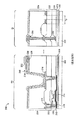
本発明の実施形態によれば、図9の従来のTFTディスプレイ構造体に比して改善された金属引き回し能力を示す表示ピクセル及び関連引き回し構造体300が提供される(例えば、図10を参照)。図10に示すように、薄膜トランジスタ308のような薄膜トランジスタは、ガラス又は他の誘電体材料から作られた透明基板302上に形成される。薄膜トランジスタ308は、図7を参照して説明された表示ピクセル薄膜トランジスタ150として働く。
In accordance with embodiments of the present invention, a display pixel and associated
光シールド304のような光シールド構造体は、基板302においてトランジスタ308の真下に形成され、そしてバックライトがトランジスタ308の動作を妨げるのを防止するように働く。緩衝層306のような1つ以上の緩衝層が基板302上及び光シールド304上に形成される。緩衝層306は、適当な透明誘電体材料から形成される。
A light shield structure, such as
トランジスタ308の活性材料310が緩衝層306上に形成される。活性材料310は、アモルファスシリコン又はポリシリコンの層である(一例として)。ゲート絶縁層312のようなゲート絶縁層が緩衝層306上及び活性材料上に形成される。ゲート絶縁体312上には、ゲート導体314のような導電性ゲート構造体が配置される。ゲート導体314は、薄膜トランジスタ308のゲート端子として働く。ゲート314の真下にある活性材料310の部分は、トランジスタ308のチャンネル領域として働く。
An
窒化シリコン層320のようなパッシベーション層がゲート絶縁層312上及びゲート314上に形成される。層320を堆積した後に、水素添加アニールプロセスを適用して、薄膜トランジスタ構造体308を不動態化する。ゲート314が形成される材料は、「M1」金属とも称される。その結果、ゲート導体314が形成される層320は、第1金属(M1)引き回し層とも称される。
A passivation layer such as a
酸化シリコンライナー321のような酸化層がパッシベーション層320上に形成される。層321は、その上に金属構造体を形成する間にエッチング停止層として働く。層321上には低k誘電体層322(例えば、誘電率kが二酸化シリコンより小さい誘電体材料から形成された層)が形成される。層322は、アクリル系ホトレジスト又は他の感光材料、シロキサン系ポリマ、シリコン系誘電体、有機材料、これらの材料の組み合わせ、及び/又は適当な低k誘電体層から形成される。
An oxide layer such as a
トランジスタの活性材料310と電気的コンタクトをなすために、構造体316及び318のようなトランジスタソース/ドレインコンタクト構造体が層322を通して形成される。コンタクト構造体316及び318は、「ビア(via)」構造体とも称される。特に、ビア316にコンタクトする活性材料310の部分は、トランジスタ308の第1のソース/ドレイン領域として働き、一方、ビア318にコンタクトする活性材料310の部分は、トランジスタ308の第2のソース/ドレイン領域として働く。アクティブなソース/ドレイン領域上にゲート導体が形成される薄膜トランジスタは、一般的に、「トップ・ゲート」薄膜トランジスタと称される。これは、単なる例示に過ぎない。必要があれば、ピクセル300は、アクティブなソース/ドレイン領域下にゲート導体が形成される「ボトム・ゲート」薄膜トランジスタ構成体を使用して形成される。
Transistor source / drain contact structures such as
トランジスタのソース/ドレイン端子を他の表示ピクセル回路に接続するために、「M2」金属引き回し経路とも称される金属引き回し構造体が層322上に形成される。一例として、層322上に形成された第1のM2金属引き回し経路は、ビア316を経て対応するデータ線(例えば、図7のデータ線D)に接続するように使用され、一方、層322上に形成された第2のM2金属引き回し経路は、ビア318を経て対応するピクセル電極ノード(例えば、図7においてピクセル電圧Vpが蓄積されるノード156)に接続するように使用される。
A metal routing structure, also referred to as an “M2” metal routing path, is formed on
層322には別の低k誘電体層が形成される。この層324は、平坦化層として働き、第2の金属(M2)引き回し層とも称される。層322と同様に、層324は、アクリル系ホトレジスト又は他の感光材料、シロキサン系ポリマ、シリコン系誘電体、有機材料、これらの材料の組み合わせ、及び/又は適当な低k誘電体層から形成される。一般的に、誘電体層を通して伝播するバックライトの透過度を最大にするために、層322及び324は、実質的に同様の屈折率を有する同じ材料で形成しなければならない(例えば、屈折率は、相違が0.1以下、0.08以下、0.05以下、0.01以下、当でなければならない)
低k誘電体平坦化層324には、Vcom層326のような共通電極層が形成される。この共通電極層326は、表示ピクセルアレイ全体をカバーする透明導電性材料のブランケット膜として、又は付加的な引き回し経路によって相互接続された個別のVcom領域として、又は容量性タッチ感知技術をサポートする他のパターン(例えば、透明導電性材料の水平及び垂直ストリップ)で形成される。Vcom電極を他のディスプレイ回路に接続するために(例えば、異なるVcom層を相互接続し、Vcom層を関連Vcomドライバ回路に接続し、Vcom層をタッチセンサ回路に接続し、等々のために)、付加的なVcom引き回し構造体328(「M3」金属引き回し経路とも称される)がVcom層326上に形成される。
A common electrode layer such as a V com layer 326 is formed on the low-k
ビア318とピクセル電極層332との間に電気的接続を形成して表示ピクセルコンタクト360(蓄積キャパシタを薄膜トランジスタ308に接続するコンタクト)を形成するために、平坦下層324には開口が形成される。ピクセル電極層332は、液晶材料160(図7)に電界を印加するフィンガー状の電極(図10には示さず)を形成するパターンとされる。ピクセル電極層332と共通電極層326との間に絶縁材料330が形成される。Vcom電極326、及びVcom電極326と重畳するピクセル電極332の一部分は、蓄積キャパシタ340を形成する(例えば、蓄積キャパシタは、Vcom層326、該Vcom層326を直接向いたピクセル電極層332の一部分、及び2つの対向する平行導体間に介在する絶縁材料330を含む)。
An opening is formed in the
一般的に、共通電極326及びピクセル電極332は、薄膜トランジスタ層の上の液晶材料へのバックライトの通過を許すインジウムスズ酸化物又は他の適当な透明材料から形成される。光シールド構造体304及びM1ゲート構造体は、モリブデン、タングステン、その2つの組み合わせのような耐高温材料、及び/又は他の適当な耐高温材料から形成される。ビア316及び318、並びにM2及びM3金属引き回し構造体は、銅、アルミニウム、銀、金、タングステン、ニッケル、他の金属、それら材料の組み合わせ、及び/又はディスプレイ14においてデータ及びコントロール信号を引き回すのに適した他の導電性材料から形成される。
Generally, the
典型的に、薄膜トランジスタ308及びそれに関連したピクセル及びVcom電極は、ディスプレイ14のアクティブエリアAA部分に形成される。アクティブエリアAAの表示ピクセルアレイ回路と、それに関連したコントロール回路(例えば、ディスプレイドライバ、ゲート線ドライバ、タッチドライバ及びセンサ回路、等)との間の引き回しは、インアクティブボーダーエリアIA内に形成される。図10に示すように、ゲート導体314は、パッシベーション層320においてゲート絶縁層312上に形成され、金属引き回し構造体350は、低k誘電体層322においてエッチング停止層321上に形成され、金属引き回し構造体352は、低k誘電体平坦化層324において低k誘電体層322上に形成され、そして金属引き回し構造体354は、平坦下層324上に形成される。
Typically, the
ゲート構造体314が形成される層は、一般的に、「M1」又は第1/最下部の金属引き回し層と称される。金属引き回し構造体352が形成される層は、一般的に、「M2」又は第2の金属引き回し層と称される。金属引き回し構造体354が形成される層は、一般的に、「M3」又は第3の金属引き回し層と称される。金属引き回し経路350は、M1及びM2の金属引き回し層間に形成された付加的な金属引き回し構造体を表わす。それ故、金属引き回し経路350が形成される層322は、中間引き回し層又はサブM2(又は「M2s」)金属引き回し層と称される。それ故、引き回し構造体350、352及び354を形成するのに使用される材料は、各々、M2s金属、M2金属、及びM3金属と称される。M3金属引き回し層上に形成される金属引き回し層がもしあれば、一般的に、順次に、M4金属引き回し層、M5金属引き回し層、M6金属引き回し層、等々と称される。
The layer in which the
上述したように、M1引き回し構造体は、高い抵抗率を示す耐高温材料から形成される。それ故、M1金属引き回し層以外の金属引き回し層に導電性経路形態を使用して信号の引き回しを遂行することが望まれる。M2s金属引き回し構造体350がパッシベーション層320上に形成される(例えば、M2s引き回し構造体を形成する前に高温アニールプロセスが遂行される)ので、M2s金属は、耐高温材料を使用して形成する必要がなく、むしろ、M2及びM3金属引き回し経路を形成するのに使用される同じ低抵抗率材料を使用して形成することができる。例えば、M2s、M2及びM3金属引き回し構造体は、銅、アルミニウム、銀、金、ニッケル、それら材料の組み合わせ、及び/又は低いシート抵抗を示し且つディスプレイ14においてデータ及びコントロール信号を引き回すのに適した他の導電性材料(即ち、シート抵抗が0.4オーム/平方未満、0.2オーム/平方未満、0.05オーム/平方未満、0.01オーム/平方未満、等の材料)から形成される。M2s及びM2金属は、実質的に同様の抵抗率レベルを示す。例えば、M2s及びM2金属引き回し経路は、両方とも、0.047オーム/平方のシート抵抗を示す。このようにM2s金属の引き回し構造体を形成することで、抵抗率の低い導電性経路を形成でき、TFTディスプレイ/タッチ構造体に対する全体的な引き回し能力を高める付加的な金属引き回し層が提供される。
As described above, the M1 routing structure is formed from a high temperature resistant material exhibiting a high resistivity. Therefore, it is desirable to perform signal routing using conductive path configurations in metal routing layers other than the M1 metal routing layer. Since the M2s
M2及びM2s金属引き回し経路が同じ信号を搬送するように並列に使用されるときには、より薄い個々の引き回し経路を形成することができる。というのは、2つの個別の経路を使用して同じ信号を搬送することで、引き回し抵抗が著しく減少するからである。図10に示すように、層322に形成される少なくとも幾つかの導電性引き回し経路350、及び層322に形成される導電性引き回し経路は、層322を通して形成されたビア351を使用して並列に短絡される。一般的に、巾を減少した金属引き回し経路を使用することは、ファンアウトピッチを減少する上で役立ち、インアクティブなボーダーエリアを減少する。
When M2 and M2s metal routing paths are used in parallel to carry the same signal, thinner individual routing paths can be formed. This is because routing resistance is significantly reduced by carrying the same signal using two separate paths. As shown in FIG. 10, at least some
隣接するM2及びM2s金属引き回し経路を使用して異なる信号を搬送するシナリオでは、インターレース型金属引き回しを実施することができる。インターレース型金属引き回しを実施するために、第1の引き回し経路350は、M2s引き回し層(例えば、層322)に形成され、そして第2の引き回し経路352は、過剰な寄生的結合作用を経験することなく第1の引き回し経路350にできるだけ接近してM2引き回し層(例えば、層324)に形成される。この解決策を使用してM2s及びM2層に3つ以上の金属引き回し経路を形成することができる。このような構成では、回路300のエリアIAにおける隣接引き回しワイヤ間の有効ピッチTp’は、図9を参照して述べたように、回路200のエリアIAにおいてM2層に形成された隣接引き回しワイヤ間のピッチTpより小さい(例えば、同じ層に隣接する金属引き回し経路を形成するだけでなく異なる層に隣接する金属引き回し経路を形成できることで、有効配線ピッチが減少される)。インターレース型引き回しによりピッチを減少することで、インアクティブなボーダーエリアを更に減少することができる。
In scenarios where adjacent M2 and M2s metal routing paths are used to carry different signals, interlaced metal routing can be implemented. To implement interlaced metal routing, a
別の適当な構成では、M2s金属引き回し層に付加的なTFTゲート構造体が形成される。図11は、M1ゲート導体314の上に付加的なゲート導体351が形成される実施例を示す。この実施例では、付加的なゲート導体351は、M2s金属引き回し層においてエッチング停止層321上に直接形成される。各表示ピクセルにおいてトランジスタ308に対する2つ以上のゲート構造体を使用することで、ピクセルアドレス能力の改善が与えられる。
In another suitable configuration, additional TFT gate structures are formed in the M2s metal routing layer. FIG. 11 shows an embodiment in which an
図12は、二重ゲートトランジスタ151のようなマルチゲート薄膜トランジスタを有する表示ピクセル110の回路図である。図12に示すように、トランジスタ151は、対応するデータ線112に結合された第1のソース/ドレイン端子と、電圧Vpが蓄積されるノード156に結合された第2のソース/ドレイン端子と、第1のゲート線114−1に結合された第1のゲート端子と、第2のゲート線114−2に結合された第2のゲート端子とを有する。第1のゲート線114−1は、トランジスタ151に第1のゲート信号G1を供給するために層320のM1金属を使用して形成され、一方、第2のゲート線114−2は、トランジスタ151に第2のゲート信号G2を供給するために層322のM2s金属を使用して形成される。図12の実施例では、ゲート線114−1は、水平に引き回され、一方、ゲート線114−2は、垂直に引き回される(即ち、ゲート線114−1は、ゲート線114−2に対して直交する)。これは、単に例示に過ぎない。別の例として、ゲート線114−1が垂直に引き回され、一方、ゲート線114−2が水平に引き回されてもよい。更に別の例として、ゲート線114−1及び114−2の両方が水平に引き回されてもよい。
FIG. 12 is a circuit diagram of a
ゲート信号G1及びG2は、トランジスタ151の動作をコントロールするために個別に使用されてもよいし又は一緒に使用されてもよい。1つの構成では、トランジスタ151をターンオンするためにゲート信号G1及びG2の両方をアサートしなければならない(例えば、トランジスタ151がデータ信号を線112から蓄積ノード156へ通過できるようにするには信号G1及びG2が同時に高にならねばならない)。別の構成では、トランジスタ151をターンオンするために2つのゲート信号の一方だけをアサートすればよい(例えば、トランジスタ151は、G1を高に駆動するか又はG2を高に駆動することでデータ信号を線112から蓄積ノード156へ通過させることができる)。図12の表示ピクセル110の残り部分(例えば、蓄積キャパシタCST、キャパシタンスCLCを有する液晶材料、及びVcom電極158)についての説明は、図7を参照して既に述べたものと同様であり、ここでは繰り返し説明しない。図12の二重ゲート表示ピクセル構成は、単なる例示に過ぎず、本発明の範囲をそれに限定するものではない。必要に応じて、3つ以上のゲートコントロール線を有する表示ピクセルを実施することができる。
Gate signals G1 and G2 may be used individually or together to control the operation of
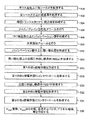
図13は、図10及び11を参照して述べたタイプのTFT構造体を形成するのに含まれる例示的ステップのフローチャートである。ステップ500において、基板302上に不透明の光シールド構造体304が形成される。ステップ520において、基板302上で光シールド304の上に1つ以上の緩衝層306が形成される。
FIG. 13 is a flowchart of exemplary steps involved in forming a TFT structure of the type described with reference to FIGS. In
ステップ504において、緩衝層306上に薄膜トランジスタ構造体308が形成される(例えば、アクティブエリアポリシリコン材料及びそれに関連したソース/ドレインドーピング及び弱くドープされたドレイン(LDD)領域、ゲート絶縁層、及びM1ゲート構造体を形成することができる)。ステップ506において、アニールプロセスを行ってソース/ドレイン領域を活性化する(例えば、ソース/ドレインドーパントを材料310において適切に拡散させる上で役立つように)。
In
ステップ508において、薄膜トランジスタ構造体308の上にパッシベーション層320(例えば、窒化シリコン層)が形成される。ステップ510において、水素添加アニールプロセスを行って、実際上、層320で薄膜トランジスタ308を不動態化する。
In
ステップ512において、パッシベーション層320の上に薄い酸化層321が形成される。層321は、その上に金属を形成する間にエッチング停止層として働く。
In
ステップ514において、エッチング停止層321にM2s金属引き回し構造体が形成される。M2s金属引き回し経路は、インアクティブボーダーエリアに形成されて、周辺信号引き回し(例えば、ゲート線引き回し、データ線引き回し、Vcom引き回し、等)を与えると共に、アクティブなディスプレイエリア内にも形成されて付加的なゲートコントロールを与える(例えば、図11及び12を参照)。
In
ステップ516において、層321上に第1の低k誘電体層322が形成される。ステップ518において、ホトリソグラフィー及びエッチングプロセスを経て第1の低k誘電体層322にコンタクトホールが形成される。ある構成では、層322は、感光材料から形成され、そして望ましいコンタクトホールを形成するように露出及び現像されるホトレジストのように使用される。
In
ステップ520において、層322上で、アクティブ及びインアクティブの両エリアでM2金属引き回し構造体がパターン化される。
In
ステップ522において、第1の低k誘電体層322上で、M2金属引き回し構造体の上に第2の低k誘電体層324が形成される。1つの構成では、第1及び第2の低k誘電体層は、同じ低k誘電体材料から形成される。他の構成では、第1及び第2の低k誘電体層が、バックライト透過度を最大にする努力において実質的に同様の屈折率を有する異なる低k誘電体材料から形成される。
In
ステップ524において、ホトリソグラフィー及びエッチングプロセスを経て第2の低k誘電体層324にコンタクトホールが形成される(例えば、層324は、耐ホトレジスト及びエッチング材料からも形成される)。ステップ526において、Vcom電極326、M3金属引き回し構造体328、蓄積キャパシタ、ピクセル電極332、及び他の表示ピクセル構造体が形成される。
In
図13のステップは、単なる例示に過ぎず、本発明の範囲をそれに限定するものではない。一般的に、LCD及び他のタイプのディスプレイにおけるTFTディスプレイ/タッチ回路は、このように形成される。製造方法を特定の順序で説明したが、上述した動作と動作との間に他のステップを遂行することもでき、上述した動作を、それらが若干異なる時間に生じるように調整することもでき、等々であることを理解されたい。 The steps in FIG. 13 are merely illustrative and do not limit the scope of the invention. In general, TFT display / touch circuits in LCDs and other types of displays are thus formed. Although the manufacturing methods have been described in a specific order, other steps can be performed between the operations described above, and the operations described above can be adjusted so that they occur at slightly different times, I hope you understand.
一実施形態によれば、基板と、基板上に形成された薄膜トランジスタと、薄膜トランジスタ上に形成されたパッシベーション層と、パッシベーション層上に形成された誘電体ライナーと、誘電体ライナー上に形成された導電性引き回し構造体とを備えたディスプレイ回路が提供される。 According to one embodiment, a substrate, a thin film transistor formed on the substrate, a passivation layer formed on the thin film transistor, a dielectric liner formed on the passivation layer, and a conductive material formed on the dielectric liner A display circuit is provided that includes a sex routing structure.
別の実施形態によれば、パッシベーション層は、窒化シリコンを含む。 According to another embodiment, the passivation layer comprises silicon nitride.
別の実施形態によれば、誘電体ライナーは、エッチング停止材料を含む。 According to another embodiment, the dielectric liner includes an etch stop material.
別の実施形態によれば、ディスプレイ回路は、誘電体ライナー上で導電性引き回し構造体の上に形成された誘電体層を含む。 According to another embodiment, a display circuit includes a dielectric layer formed over a conductive routing structure on a dielectric liner.
別の実施形態によれば、誘電体層は、低k誘電体材料を含む。 According to another embodiment, the dielectric layer comprises a low-k dielectric material.
別の実施形態によれば、ディスプレイ回路は、誘電体層上に形成された付加的な導電性引き回し構造体を含み、誘電体ライナー上に形成された導電性引き回し構造体、及び誘電体層上に形成された付加的な導電性引き回し構造体は、実質的に同様の抵抗率を示す。 According to another embodiment, the display circuit includes an additional conductive routing structure formed on the dielectric layer, the conductive routing structure formed on the dielectric liner, and on the dielectric layer. The additional conductive routing structure formed in FIG. 4 exhibits substantially similar resistivity.
別の実施形態によれば、薄膜トランジスタは、導電性引き回し構造体より大きなシート抵抗を示す導電性材料から形成されたゲート構造体を含む。 According to another embodiment, the thin film transistor includes a gate structure formed from a conductive material that exhibits a greater sheet resistance than the conductive routing structure.
別の実施形態によれば、薄膜トランジスタのゲート構造体は、パッシベーション層に形成される。 According to another embodiment, the thin film transistor gate structure is formed in a passivation layer.
一実施形態によれば、ディスプレイ回路を製造する方法において、基板上に薄膜トランジスタを形成し、薄膜トランジスタ上に低k誘電体層を形成し、及び低k誘電体層に導電性引き回し経路を形成することを含む方法が提供される。 According to one embodiment, in a method of manufacturing a display circuit, a thin film transistor is formed on a substrate, a low k dielectric layer is formed on the thin film transistor, and a conductive routing path is formed in the low k dielectric layer. Is provided.
別の実施形態によれば、前記方法は、薄膜トランジスタ上にパッシベーション層を形成することを含み、そのパッシベーション層は、薄膜トランジスタと低k誘電体層との間に介在される。 According to another embodiment, the method includes forming a passivation layer on the thin film transistor, the passivation layer being interposed between the thin film transistor and the low-k dielectric layer.
別の実施形態によれば、前記方法は、パッシベーション層と低k誘電体層との間に介在する酸化物ライナーを形成することを含み、その酸化物ライナー上に導電性引き回し経路が形成される。 According to another embodiment, the method includes forming an oxide liner interposed between a passivation layer and a low-k dielectric layer, and a conductive routing path is formed on the oxide liner. .
別の実施形態によれば、前記方法は、低k誘電体層上に別の誘電体層を形成し、及びその別の誘電体層上にディスプレイ回路のための共通電極を形成することを含む。 According to another embodiment, the method includes forming another dielectric layer on the low-k dielectric layer and forming a common electrode for the display circuit on the other dielectric layer. .
別の実施形態によれば、前記方法は、低k誘電体層上に付加的な導電性引き回し経路を形成することを含み、導電性引き回し経路及びその付加的な導電性引き回し経路は、低k誘電体層を通して形成されたビアを使用して並列に短絡される。 According to another embodiment, the method includes forming an additional conductive routing path on the low-k dielectric layer, wherein the conductive routing path and the additional conductive routing path are low k. Shorted in parallel using vias formed through the dielectric layer.
別の実施形態によれば、前記方法は、低k誘電体層上に付加的な導電性引き回し経路を形成することを含み、導電性引き回し経路及びその付加的な導電性引き回し経路は、配線ピッチを減少するようにインターレースされる。 According to another embodiment, the method includes forming an additional conductive routing path on the low-k dielectric layer, the conductive routing path and the additional conductive routing path being a wiring pitch. Is interlaced to reduce
別の実施形態によれば、前記方法は、低k誘電体層上に別の誘電体層を形成し、及びその別の誘電体層上に蓄積キャパシタを形成することを含む。 According to another embodiment, the method includes forming another dielectric layer on the low-k dielectric layer and forming a storage capacitor on the other dielectric layer.
一実施形態によれば、基板と、基板上に形成された薄膜トランジスタとを備え、薄膜トランジスタは、基板上に形成されたソース/ドレイン構造体、ソース/ドレイン構造体上に形成された第1ゲート構造体、及び第1ゲート構造体上に形成された第2ゲート構造体を含む電子装置ディスプレイ構造体が提供される。 According to one embodiment, a substrate comprises a substrate and a thin film transistor formed on the substrate, the thin film transistor comprising a source / drain structure formed on the substrate, a first gate structure formed on the source / drain structure. There is provided an electronic device display structure including a body and a second gate structure formed on the first gate structure.
別の実施形態によれば、第1ゲート構造体は、第1材料から形成され、そして第2ゲート構造体は、第1材料とは異なる第2材料から形成される。 According to another embodiment, the first gate structure is formed from a first material and the second gate structure is formed from a second material that is different from the first material.
別の実施形態によれば、第1材料は、第2材料より大きなシート抵抗を示す。 According to another embodiment, the first material exhibits a greater sheet resistance than the second material.
別の実施形態によれば、電子装置ディスプレイ構造体は、第1ゲート構造体上に形成されたパッシベーション層と、そのパッシベーション層上に形成された誘電体ライナーとを備え、その誘電体ライナー上に第2ゲート構造体が形成される。 According to another embodiment, an electronic device display structure comprises a passivation layer formed on a first gate structure, and a dielectric liner formed on the passivation layer, on the dielectric liner. A second gate structure is formed.
別の実施形態によれば、電子装置ディスプレイ構造体は、第1ゲート構造体に結合された第1ゲート線と、第2ゲート構造体に結合された第2ゲート線とを備え、第1ゲート線は、第2ゲート線に直交する。 According to another embodiment, an electronic device display structure comprises a first gate line coupled to a first gate structure and a second gate line coupled to a second gate structure, wherein the first gate The line is orthogonal to the second gate line.
以上、本発明の原理を例示したが、当業者であれば、本発明の精神及び範囲から逸脱せずに種々の変更がなされ得ることが明らかであろう。上述した実施形態は、個々に具現化されてもよいし又は任意の組み合わせで具現化されてもよい。 While the principles of the invention have been illustrated above, it will be apparent to those skilled in the art that various modifications can be made without departing from the spirit and scope of the invention. The embodiments described above may be embodied individually or in any combination.
10:電子装置
12:ハウジング
14:ディスプレイ
18:キーボード
20:タッチパッド
28:カラーフィルタ(CF)層
29:カラーフィルタ基板
30:薄膜トランジスタ(TFT)層
31:カラーフィルタアレイ
32:液晶(LC)層
39、40:偏光層
41:バックライトユニット
45:黒いマスク材料
100:装置コンポーネント
102:入力/出力回路
104:コントロール回路
110:表示ピクセル
112:データ線
114:ゲート線
116:ゲートディスプレイ回路
118:ディスプレイドライバ回路
119:経路
120:アクティブディスプレイ領域
122:ピクセルアレイ
300:表示ピクセル及び関連引き回し構造体
302:透明基板
306:緩衝層
308:薄膜トランジスタ
310:活性材料
312:ゲート絶縁体
314:ゲート導体
316、318:コンタクト構造体
320:窒化シリコン層(パッシベーション層)
321:酸化シリコンライナー
322:低k誘電体層
324:低k誘電体平坦化層
326:Vcom層
328:Vcom引き回し構造体
330:絶縁材料
332:ピクセル電極層
340:蓄積キャパシタ
350:金属引き回し経路
360:表示ピクセルコンタクト
AA:アクティブエリア
IA:インアクティブエリア
10: Electronic device 12: Housing 14: Display 18: Keyboard 20: Touch pad 28: Color filter (CF) layer 29: Color filter substrate 30: Thin film transistor (TFT) layer 31: Color filter array 32: Liquid crystal (LC)
321: Silicon oxide liner 322: Low-k dielectric layer 324: Low-k dielectric planarizing layer 326: V com layer 328: V com routing structure 330: Insulating material 332: Pixel electrode layer 340: Storage capacitor 350: Metal routing Path 360: Display pixel contact AA: Active area IA: Inactive area
Claims (20)
前記基板上に形成された薄膜トランジスタと、
前記薄膜トランジスタ上に形成されたパッシベーション層と、
前記パッシベーション層上に形成された誘電体ライナーと、
前記誘電体ライナー上に形成された導電性引き回し構造体と、
を備えたディスプレイ回路。 A substrate,
A thin film transistor formed on the substrate;
A passivation layer formed on the thin film transistor;
A dielectric liner formed on the passivation layer;
A conductive routing structure formed on the dielectric liner;
Display circuit equipped with.
基板上に薄膜トランジスタを形成し、
前記薄膜トランジスタ上に低k誘電体層を形成し、及び
前記低k誘電体層に導電性引き回し経路を形成する、
ことを含む方法。 In a method of manufacturing a display circuit,
A thin film transistor is formed on the substrate,
Forming a low-k dielectric layer on the thin film transistor, and forming a conductive routing path in the low-k dielectric layer;
A method involving that.
前記別の誘電体層上にディスプレイ回路のための共通電極を形成する、
ことを更に含む、請求項9に記載の方法。 Forming another dielectric layer on the low-k dielectric layer, and forming a common electrode for a display circuit on the another dielectric layer;
10. The method of claim 9, further comprising:
前記別の誘電体層上に蓄積キャパシタを形成する、
ことを更に含む請求項9に記載の方法。 Forming another dielectric layer on the low-k dielectric layer, and forming a storage capacitor on the other dielectric layer;
The method of claim 9 further comprising:
前記基板上に形成された薄膜トランジスタと、
を備え、前記薄膜トランジスタは、
前記基板上に形成されたソース/ドレイン構造体、
前記ソース/ドレイン構造体上に形成された第1ゲート構造体、及び
前記第1ゲート構造体上に形成された第2ゲート構造体、
を含む電子装置ディスプレイ構造体。 A substrate,
A thin film transistor formed on the substrate;
The thin film transistor comprises:
A source / drain structure formed on the substrate;
A first gate structure formed on the source / drain structure; and a second gate structure formed on the first gate structure;
An electronic device display structure comprising:
前記パッシベーション層上に形成された誘電体ライナー、
を更に備え、前記誘電体ライナー上に前記第2ゲート構造体が形成される、請求項16に記載の電子装置ディスプレイ構造体。 A passivation layer formed on the first gate structure, and a dielectric liner formed on the passivation layer;
The electronic device display structure of claim 16, further comprising: the second gate structure formed on the dielectric liner.
前記第2ゲート構造体に結合された第2ゲート線、
を備え、前記第1ゲート線は、前記第2ゲート線に直交する、請求項16に記載の電子装置ディスプレイ構造体。 A first gate line coupled to the first gate structure; and a second gate line coupled to the second gate structure;
The electronic device display structure of claim 16, wherein the first gate line is orthogonal to the second gate line.
Applications Claiming Priority (2)
| Application Number | Priority Date | Filing Date | Title |
|---|---|---|---|
| US14/150,458 US9704888B2 (en) | 2014-01-08 | 2014-01-08 | Display circuitry with reduced metal routing resistance |
| US14/150,458 | 2014-01-08 |
Related Child Applications (1)
| Application Number | Title | Priority Date | Filing Date |
|---|---|---|---|
| JP2017031730A Division JP6362721B2 (en) | 2014-01-08 | 2017-02-23 | Display circuit with reduced metal routing resistance |
Publications (2)
| Publication Number | Publication Date |
|---|---|
| JP2015129941A true JP2015129941A (en) | 2015-07-16 |
| JP6313716B2 JP6313716B2 (en) | 2018-04-18 |
Family
ID=53125388
Family Applications (3)
| Application Number | Title | Priority Date | Filing Date |
|---|---|---|---|
| JP2015002350A Expired - Fee Related JP6313716B2 (en) | 2014-01-08 | 2015-01-08 | Display circuit with reduced metal routing resistance |
| JP2017031730A Expired - Fee Related JP6362721B2 (en) | 2014-01-08 | 2017-02-23 | Display circuit with reduced metal routing resistance |
| JP2018120556A Expired - Fee Related JP6772217B2 (en) | 2014-01-08 | 2018-06-26 | Display circuit with reduced metal routing resistance |
Family Applications After (2)
| Application Number | Title | Priority Date | Filing Date |
|---|---|---|---|
| JP2017031730A Expired - Fee Related JP6362721B2 (en) | 2014-01-08 | 2017-02-23 | Display circuit with reduced metal routing resistance |
| JP2018120556A Expired - Fee Related JP6772217B2 (en) | 2014-01-08 | 2018-06-26 | Display circuit with reduced metal routing resistance |
Country Status (5)
| Country | Link |
|---|---|
| US (1) | US9704888B2 (en) |
| JP (3) | JP6313716B2 (en) |
| KR (2) | KR20150083043A (en) |
| CN (2) | CN104599651B (en) |
| DE (1) | DE102014226616A1 (en) |
Cited By (2)
| Publication number | Priority date | Publication date | Assignee | Title |
|---|---|---|---|---|
| JP2018032827A (en) * | 2016-08-26 | 2018-03-01 | 大日本印刷株式会社 | Wiring board and display device |
| JP2019505999A (en) * | 2016-01-28 | 2019-02-28 | 武漢華星光電技術有限公司 | Low temperature polysilicon array substrate manufacturing method |
Families Citing this family (29)
| Publication number | Priority date | Publication date | Assignee | Title |
|---|---|---|---|---|
| US9704888B2 (en) | 2014-01-08 | 2017-07-11 | Apple Inc. | Display circuitry with reduced metal routing resistance |
| CN103928472A (en) * | 2014-03-26 | 2014-07-16 | 京东方科技集团股份有限公司 | Array substrate, manufacturing method of array substrate and display device |
| KR102205856B1 (en) * | 2014-06-11 | 2021-01-21 | 삼성디스플레이 주식회사 | Organic light emitting diode display device including sensors |
| TWI578544B (en) * | 2014-12-02 | 2017-04-11 | 鴻海精密工業股份有限公司 | Thin film transistor and display array substrate using the same |
| KR102411327B1 (en) * | 2015-01-02 | 2022-06-21 | 삼성디스플레이 주식회사 | Display device |
| KR20160086016A (en) * | 2015-01-08 | 2016-07-19 | 삼성디스플레이 주식회사 | Thin film transistor array panel and manufacturing method therfor |
| KR102263603B1 (en) * | 2015-01-20 | 2021-06-10 | 삼성디스플레이 주식회사 | Organic light emitting diode display |
| CN104698711B (en) * | 2015-04-01 | 2018-06-01 | 上海天马微电子有限公司 | Array substrate, display panel and electronic equipment |
| CN104777692B (en) | 2015-05-08 | 2018-09-04 | 厦门天马微电子有限公司 | Array substrate and production method, touch-control display panel |
| KR102430817B1 (en) * | 2015-11-05 | 2022-08-10 | 삼성디스플레이 주식회사 | display device |
| KR102485707B1 (en) * | 2016-01-29 | 2023-01-09 | 삼성디스플레이 주식회사 | Organic light emitting display device |
| CN106094373A (en) * | 2016-06-02 | 2016-11-09 | 武汉华星光电技术有限公司 | TFT substrate and preparation method thereof |
| US10288871B1 (en) * | 2016-06-27 | 2019-05-14 | Amazon Technologies, Inc. | Organic material layer as light shield for thin film transistor channel |
| TWI625847B (en) * | 2016-09-09 | 2018-06-01 | 友達光電股份有限公司 | Pixel structure and its making method |
| KR102376412B1 (en) * | 2017-07-14 | 2022-03-22 | 삼성디스플레이 주식회사 | Touch sensor and display device including the same |
| US11222931B2 (en) * | 2017-07-28 | 2022-01-11 | Sharp Kabushiki Kaisha | Display device |
| US10566354B2 (en) * | 2018-02-26 | 2020-02-18 | Wuhan China Star Optoelectronics Technology Co., Ltd. | Array substrate, touch display screen and manufacturing method of array substrate |
| CN108540600B (en) * | 2018-03-30 | 2020-09-18 | Oppo广东移动通信有限公司 | electronic device |
| US20240021629A1 (en) * | 2018-04-27 | 2024-01-18 | Boe Technology Group Co., Ltd. | Array substrate, method of manufacturing the same and method of improving performance of the same, display panel and display device |
| US11187834B2 (en) | 2018-06-14 | 2021-11-30 | Intevac, Inc. | Multi-colored dielectric coating |
| US10852607B2 (en) | 2018-08-21 | 2020-12-01 | Apple Inc. | Displays with data lines that accommodate openings |
| US11852938B2 (en) | 2018-08-21 | 2023-12-26 | Apple Inc. | Displays with data lines that accommodate openings |
| CN109768054B (en) * | 2019-02-25 | 2020-11-10 | 云谷(固安)科技有限公司 | Array substrate and display screen |
| US11036322B2 (en) * | 2019-06-24 | 2021-06-15 | Wuhan China Star Optoelectronics Technology Co., Ltd | Array substrate and method of manufacturing same |
| CN112309280B (en) * | 2019-07-31 | 2022-04-29 | 北京梦之墨科技有限公司 | Electroluminescent sheet with controllable pattern, manufacturing method thereof and light-emitting device |
| TW202329672A (en) * | 2021-09-07 | 2023-07-16 | 美商歐柏西迪恩感應器公司 | Sensor design |
| CN114355686B (en) | 2022-01-07 | 2023-08-01 | 武汉华星光电技术有限公司 | Array substrate and liquid crystal display panel |
| KR102923662B1 (en) * | 2022-05-04 | 2026-02-05 | 경희대학교 산학협력단 | Display pixel circuit using ferroelectric thin film transistor and driving method thereof |
| US11966544B2 (en) | 2022-07-29 | 2024-04-23 | Apple Inc. | Data line shielding for electronic device displays with touch sensors |
Citations (10)
| Publication number | Priority date | Publication date | Assignee | Title |
|---|---|---|---|---|
| JPH0682826A (en) * | 1992-09-03 | 1994-03-25 | Sharp Corp | Active matrix substrate and manufacturing method thereof |
| JP2001077373A (en) * | 1999-07-06 | 2001-03-23 | Semiconductor Energy Lab Co Ltd | Semiconductor device and manufacturing method thereof |
| JP2002094065A (en) * | 2000-09-11 | 2002-03-29 | Matsushita Electric Ind Co Ltd | Thin film transistor, liquid crystal display device using the same, and image display application device using the liquid crystal display device |
| JP2004253596A (en) * | 2003-02-20 | 2004-09-09 | Nec Corp | Thin film transistor substrate and method of manufacturing the same |
| JP2005031645A (en) * | 2003-06-16 | 2005-02-03 | Semiconductor Energy Lab Co Ltd | Display device and manufacturing method thereof |
| JP2005173579A (en) * | 2003-11-21 | 2005-06-30 | Semiconductor Energy Lab Co Ltd | Display device |
| WO2006016662A1 (en) * | 2004-08-11 | 2006-02-16 | Sanyo Electric Co., Ltd. | Semiconductor element matrix array and manufacturing method of the same, and display panel |
| JP2008034367A (en) * | 2006-07-04 | 2008-02-14 | Semiconductor Energy Lab Co Ltd | Display device |
| JP2011164329A (en) * | 2010-02-09 | 2011-08-25 | Sony Corp | Electro-optical display panel |
| JP2011186362A (en) * | 2010-03-11 | 2011-09-22 | Seiko Epson Corp | Electro-optic device and electronic device |
Family Cites Families (45)
| Publication number | Priority date | Publication date | Assignee | Title |
|---|---|---|---|---|
| JPH1197698A (en) | 1997-09-24 | 1999-04-09 | Toshiba Corp | Thin film transistor |
| US6365917B1 (en) | 1998-11-25 | 2002-04-02 | Semiconductor Energy Laboratory Co., Ltd. | Semiconductor device |
| JP2000258798A (en) * | 1999-03-05 | 2000-09-22 | Sanyo Electric Co Ltd | Display device |
| TW518637B (en) * | 1999-04-15 | 2003-01-21 | Semiconductor Energy Lab | Electro-optical device and electronic equipment |
| TW478014B (en) | 1999-08-31 | 2002-03-01 | Semiconductor Energy Lab | Semiconductor device and method of manufacturing thereof |
| KR100675924B1 (en) | 1999-11-09 | 2007-02-01 | 비오이 하이디스 테크놀로지 주식회사 | Liquid crystal display device having high opening ratio and high transmittance |
| JP3861590B2 (en) * | 2000-11-21 | 2006-12-20 | セイコーエプソン株式会社 | Electro-optical device and projector |
| TW525216B (en) | 2000-12-11 | 2003-03-21 | Semiconductor Energy Lab | Semiconductor device, and manufacturing method thereof |
| JP4884586B2 (en) | 2000-12-18 | 2012-02-29 | 株式会社 日立ディスプレイズ | Liquid crystal display |
| SG118117A1 (en) | 2001-02-28 | 2006-01-27 | Semiconductor Energy Lab | Semiconductor device and manufacturing method thereof |
| JP3702860B2 (en) | 2001-04-16 | 2005-10-05 | セイコーエプソン株式会社 | Electro-optical device, manufacturing method thereof, and electronic apparatus |
| JP2003255381A (en) * | 2001-12-28 | 2003-09-10 | Advanced Display Inc | Image display device and method of manufacturing the same |
| KR100846464B1 (en) * | 2002-05-28 | 2008-07-17 | 삼성전자주식회사 | Amorphous Silicon Thin Film Transistor-Liquid Crystal Display and Manufacturing Method Thereof |
| JP4006284B2 (en) | 2002-07-17 | 2007-11-14 | 株式会社 日立ディスプレイズ | Liquid crystal display |
| KR100968560B1 (en) | 2003-01-07 | 2010-07-08 | 삼성전자주식회사 | Metal wiring formation method of thin film transistor substrate and thin film transistor substrate |
| US7161184B2 (en) * | 2003-06-16 | 2007-01-09 | Semiconductor Energy Laboratory Co., Ltd. | Display device and method for manufacturing the same |
| JP2005057242A (en) | 2003-07-18 | 2005-03-03 | Seiko Epson Corp | Thin film transistor, active matrix substrate, display device, and electronic device |
| US20060082536A1 (en) * | 2004-10-04 | 2006-04-20 | Jun Koyama | Display device and driving method |
| US7999994B2 (en) * | 2005-02-23 | 2011-08-16 | Pixtronix, Inc. | Display apparatus and methods for manufacture thereof |
| JP4799952B2 (en) * | 2005-08-08 | 2011-10-26 | 三菱電機株式会社 | Liquid crystal display |
| TWI322288B (en) * | 2006-03-07 | 2010-03-21 | Au Optronics Corp | Manufacture method of pixel array substrate |
| JP2008112136A (en) * | 2006-10-04 | 2008-05-15 | Mitsubishi Electric Corp | Display device and manufacturing method thereof |
| JP2008305199A (en) | 2007-06-07 | 2008-12-18 | Fujitsu Component Ltd | Input system and program |
| WO2009117438A2 (en) | 2008-03-20 | 2009-09-24 | Applied Materials, Inc. | Process to make metal oxide thin film transistor array with etch stopping layer |
| TWI374510B (en) | 2008-04-18 | 2012-10-11 | Au Optronics Corp | Gate driver on array of a display and method of making device of a display |
| US8258511B2 (en) | 2008-07-02 | 2012-09-04 | Applied Materials, Inc. | Thin film transistors using multiple active channel layers |
| KR101024535B1 (en) | 2008-07-07 | 2011-03-31 | 엘지디스플레이 주식회사 | LCD Display |
| JP4798186B2 (en) * | 2008-08-21 | 2011-10-19 | セイコーエプソン株式会社 | Electro-optical device and electronic apparatus |
| JP5176814B2 (en) * | 2008-09-22 | 2013-04-03 | セイコーエプソン株式会社 | Electro-optical device, electronic apparatus, and method of manufacturing electro-optical device |
| CN102265405B (en) | 2008-12-24 | 2015-09-23 | 3M创新有限公司 | Enhanced Stability in Metal Oxide Semiconductor Thin Film Transistors |
| US8198666B2 (en) * | 2009-02-20 | 2012-06-12 | Semiconductor Energy Laboratory Co., Ltd. | Semiconductor device including a nonvolatile memory element having first, second and third insulating films |
| BR112012002178A2 (en) | 2009-07-28 | 2016-05-31 | Sharp Kk | wiring board, method of fabrication, display panel, and display device |
| CN102473734B (en) | 2009-07-31 | 2015-08-12 | 株式会社半导体能源研究所 | Semiconductor device and manufacturing method thereof |
| KR102295450B1 (en) | 2009-10-09 | 2021-08-27 | 가부시키가이샤 한도오따이 에네루기 켄큐쇼 | Display device |
| US8617986B2 (en) | 2009-11-09 | 2013-12-31 | Taiwan Semiconductor Manufacturing Company, Ltd. | Integrated circuits and methods for forming the integrated circuits |
| US8617946B2 (en) | 2009-11-11 | 2013-12-31 | Taiwan Semiconductor Manufacturing Company, Ltd. | Integrated circuits including metal gates and fabrication methods thereof |
| KR101654324B1 (en) | 2009-12-28 | 2016-09-09 | 엘지디스플레이 주식회사 | Liquid Crystal Display device and Fabricating Method thereof |
| CN111326435B (en) | 2010-04-23 | 2023-12-01 | 株式会社半导体能源研究所 | Semiconductor device manufacturing method |
| WO2011162104A1 (en) * | 2010-06-25 | 2011-12-29 | Semiconductor Energy Laboratory Co., Ltd. | Semiconductor device and method for driving the same |
| CN103718231B (en) * | 2011-08-09 | 2018-09-14 | 夏普株式会社 | Display device |
| US9318484B2 (en) * | 2013-02-20 | 2016-04-19 | Semiconductor Energy Laboratory Co., Ltd. | Semiconductor device |
| KR102018284B1 (en) * | 2013-02-28 | 2019-09-05 | 삼성디스플레이 주식회사 | Substrate formed thin film transistor array and organic light emitting diode display |
| KR102173707B1 (en) * | 2013-05-31 | 2020-11-04 | 삼성디스플레이 주식회사 | Thin film transistor and organic light emitting diode display including the same |
| KR102296294B1 (en) * | 2013-11-05 | 2021-09-01 | 삼성디스플레이 주식회사 | Thin film transistor array panel and method for manufacturing the same |
| US9704888B2 (en) | 2014-01-08 | 2017-07-11 | Apple Inc. | Display circuitry with reduced metal routing resistance |
-
2014
- 2014-01-08 US US14/150,458 patent/US9704888B2/en active Active
- 2014-12-19 DE DE102014226616.5A patent/DE102014226616A1/en not_active Ceased
-
2015
- 2015-01-07 CN CN201510008080.XA patent/CN104599651B/en not_active Expired - Fee Related
- 2015-01-07 CN CN201520009770.2U patent/CN204391112U/en not_active Expired - Fee Related
- 2015-01-08 KR KR1020150002490A patent/KR20150083043A/en not_active Ceased
- 2015-01-08 JP JP2015002350A patent/JP6313716B2/en not_active Expired - Fee Related
-
2017
- 2017-02-23 JP JP2017031730A patent/JP6362721B2/en not_active Expired - Fee Related
- 2017-04-13 KR KR1020170047940A patent/KR101837343B1/en not_active Expired - Fee Related
-
2018
- 2018-06-26 JP JP2018120556A patent/JP6772217B2/en not_active Expired - Fee Related
Patent Citations (10)
| Publication number | Priority date | Publication date | Assignee | Title |
|---|---|---|---|---|
| JPH0682826A (en) * | 1992-09-03 | 1994-03-25 | Sharp Corp | Active matrix substrate and manufacturing method thereof |
| JP2001077373A (en) * | 1999-07-06 | 2001-03-23 | Semiconductor Energy Lab Co Ltd | Semiconductor device and manufacturing method thereof |
| JP2002094065A (en) * | 2000-09-11 | 2002-03-29 | Matsushita Electric Ind Co Ltd | Thin film transistor, liquid crystal display device using the same, and image display application device using the liquid crystal display device |
| JP2004253596A (en) * | 2003-02-20 | 2004-09-09 | Nec Corp | Thin film transistor substrate and method of manufacturing the same |
| JP2005031645A (en) * | 2003-06-16 | 2005-02-03 | Semiconductor Energy Lab Co Ltd | Display device and manufacturing method thereof |
| JP2005173579A (en) * | 2003-11-21 | 2005-06-30 | Semiconductor Energy Lab Co Ltd | Display device |
| WO2006016662A1 (en) * | 2004-08-11 | 2006-02-16 | Sanyo Electric Co., Ltd. | Semiconductor element matrix array and manufacturing method of the same, and display panel |
| JP2008034367A (en) * | 2006-07-04 | 2008-02-14 | Semiconductor Energy Lab Co Ltd | Display device |
| JP2011164329A (en) * | 2010-02-09 | 2011-08-25 | Sony Corp | Electro-optical display panel |
| JP2011186362A (en) * | 2010-03-11 | 2011-09-22 | Seiko Epson Corp | Electro-optic device and electronic device |
Cited By (2)
| Publication number | Priority date | Publication date | Assignee | Title |
|---|---|---|---|---|
| JP2019505999A (en) * | 2016-01-28 | 2019-02-28 | 武漢華星光電技術有限公司 | Low temperature polysilicon array substrate manufacturing method |
| JP2018032827A (en) * | 2016-08-26 | 2018-03-01 | 大日本印刷株式会社 | Wiring board and display device |
Also Published As
| Publication number | Publication date |
|---|---|
| CN104599651B (en) | 2017-03-22 |
| JP2018146989A (en) | 2018-09-20 |
| JP6772217B2 (en) | 2020-10-21 |
| US9704888B2 (en) | 2017-07-11 |
| KR20170047198A (en) | 2017-05-04 |
| CN104599651A (en) | 2015-05-06 |
| DE102014226616A1 (en) | 2015-07-09 |
| JP6313716B2 (en) | 2018-04-18 |
| KR20150083043A (en) | 2015-07-16 |
| KR101837343B1 (en) | 2018-03-09 |
| JP6362721B2 (en) | 2018-07-25 |
| CN204391112U (en) | 2015-06-10 |
| US20150194443A1 (en) | 2015-07-09 |
| JP2017107595A (en) | 2017-06-15 |
Similar Documents
| Publication | Publication Date | Title |
|---|---|---|
| JP6362721B2 (en) | Display circuit with reduced metal routing resistance | |
| US10210830B2 (en) | Display having vertical gate line extensions and minimized borders | |
| US9977276B2 (en) | Array substrate, display panel and display device | |
| CN204360062U (en) | Display pixel circuits and display pixel structure | |
| US8994906B2 (en) | Display with multilayer and embedded signal lines | |
| US10019090B2 (en) | Display with touch sensor circuitry | |
| TWI397756B (en) | Active array substrate, liquid crystal display panel and method for manufacturing the same | |
| CN101561609A (en) | Active array substrate, liquid crystal display panel and method for manufacturing active array substrate | |
| JP2017122913A (en) | Display panel | |
| CN116339019A (en) | touch display device | |
| US12405502B2 (en) | Pixel layouts for electronic device displays | |
| CN115472664B (en) | Display panel and display device | |
| US20240065057A1 (en) | Fanout Lines with Shielding in an Active Area | |
| JP2019066719A (en) | Display panel | |
| CN115691314A (en) | electronic device |
Legal Events
| Date | Code | Title | Description |
|---|---|---|---|
| A977 | Report on retrieval |
Free format text: JAPANESE INTERMEDIATE CODE: A971007 Effective date: 20160108 |
|
| A131 | Notification of reasons for refusal |
Free format text: JAPANESE INTERMEDIATE CODE: A131 Effective date: 20160201 |
|
| A521 | Request for written amendment filed |
Free format text: JAPANESE INTERMEDIATE CODE: A523 Effective date: 20160502 |
|
| A02 | Decision of refusal |
Free format text: JAPANESE INTERMEDIATE CODE: A02 Effective date: 20161031 |
|
| A521 | Request for written amendment filed |
Free format text: JAPANESE INTERMEDIATE CODE: A523 Effective date: 20170223 |
|
| A911 | Transfer to examiner for re-examination before appeal (zenchi) |
Free format text: JAPANESE INTERMEDIATE CODE: A911 Effective date: 20170404 |
|
| A912 | Re-examination (zenchi) completed and case transferred to appeal board |
Free format text: JAPANESE INTERMEDIATE CODE: A912 Effective date: 20170609 |
|
| A521 | Request for written amendment filed |
Free format text: JAPANESE INTERMEDIATE CODE: A523 Effective date: 20180117 |
|
| A61 | First payment of annual fees (during grant procedure) |
Free format text: JAPANESE INTERMEDIATE CODE: A61 Effective date: 20180323 |
|
| R150 | Certificate of patent or registration of utility model |
Ref document number: 6313716 Country of ref document: JP Free format text: JAPANESE INTERMEDIATE CODE: R150 |
|
| R250 | Receipt of annual fees |
Free format text: JAPANESE INTERMEDIATE CODE: R250 |
|
| R250 | Receipt of annual fees |
Free format text: JAPANESE INTERMEDIATE CODE: R250 |
|
| LAPS | Cancellation because of no payment of annual fees |