JP2015141902A - Impedance element, method of manufacturing the same, noise filter using the same, and method of manufacturing the same - Google Patents
Impedance element, method of manufacturing the same, noise filter using the same, and method of manufacturing the same Download PDFInfo
- Publication number
- JP2015141902A JP2015141902A JP2014011934A JP2014011934A JP2015141902A JP 2015141902 A JP2015141902 A JP 2015141902A JP 2014011934 A JP2014011934 A JP 2014011934A JP 2014011934 A JP2014011934 A JP 2014011934A JP 2015141902 A JP2015141902 A JP 2015141902A
- Authority
- JP
- Japan
- Prior art keywords
- conductor
- impedance element
- manufacturing
- tip
- connection
- Prior art date
- Legal status (The legal status is an assumption and is not a legal conclusion. Google has not performed a legal analysis and makes no representation as to the accuracy of the status listed.)
- Pending
Links
Images







Landscapes
- Filters And Equalizers (AREA)
- Coils Or Transformers For Communication (AREA)
Abstract
【課題】高いインダクタンス値を有し、大電流を流すことのできるインピーダンス素子及びそれを用いたノイズフィルタを製造する。【解決手段】少なくとも4本の偶数本の貫通孔(4)を有する直方体状の磁性体(3)を形成する。逆U字状の導体(5)を形成する。貫通孔に導体の先端を挿入する。対角の2本を除く導体を電気的に接続する。すると、インピーダンス素子(2)内部に螺旋状コイルが形成される。この製造方法により、高いインダクタンス値を有し、大電流を流すことができるインピーダンス素子を得られる。さらに、前記インピーダンス素子を1個又は2個、ケース(6)と裏蓋(7)の内部に収納すると、前述の性能を有するノイズフィルタ(1)を製造できる。【選択図】図1An impedance element having a high inductance value and capable of flowing a large current and a noise filter using the impedance element are manufactured. A rectangular parallelepiped magnetic body (3) having at least four even number of through holes (4) is formed. An inverted U-shaped conductor (5) is formed. Insert the tip of the conductor into the through hole. The conductors other than the two diagonals are electrically connected. Then, a spiral coil is formed inside the impedance element (2). By this manufacturing method, an impedance element having a high inductance value and allowing a large current to flow can be obtained. Further, when one or two impedance elements are housed inside the case (6) and the back cover (7), the noise filter (1) having the above-described performance can be manufactured. [Selection] Figure 1
Description
本発明は、スイッチング電源や電子機器のDC電源等の入出力部におけるコモンモードノイズ、ディファレンシャルモードノイズを除去するのに適したインピーダンス素子及びその製造方法並びにそれを用いたノイズフィルタ及びその製造方法に関する。 The present invention relates to an impedance element suitable for removing common mode noise and differential mode noise in an input / output unit such as a switching power supply or a DC power supply of an electronic device, a manufacturing method thereof, a noise filter using the impedance element, and a manufacturing method thereof. .
従来から、電子機器への入力電流に含まれる高周波の電圧変化を除去し、安定した電気信号を電子機器に供給するための素子であるノイズフィルタやインピーダンス素子として、特許文献1(特許第2836039号公報)に示すインピーダンス素子が公知であり、この種のインピーダンス素子は、図14に示すように導体が磁性体を巻回してチョークコイルを形成する構造となっている。 Conventionally, Patent Document 1 (Patent No. 2836039) is known as a noise filter or impedance element that is an element for removing a high-frequency voltage change included in an input current to an electronic device and supplying a stable electric signal to the electronic device. As shown in FIG. 14, this type of impedance element has a structure in which a conductor is wound around a magnetic material to form a choke coil.
すなわち前記公知のインピーダンス素子51は、磁性体52に貫通孔53を設け、前記貫通孔53内に形成された内部導電路54と前記磁性体53の表面に形成された表面導電路55とによって螺旋状の導電路を形成している。この螺旋状の導電路により、前記公知のインピーダンス素子51は、高いインダクタンスを得られるという優れた効果を発揮する。
That is, the known
しかしながら、前記公知のインピーダンス素子51は、前記内部導電路54、前記表面導電路55及び外部電極56が焼き付けやめっき等の方法にて形成されているため、結果としてインピーダンス素子全体の抵抗値が高くなってしまい、大電流を流すことができないという問題があった。したがって、本発明の課題は、大電流を流すことのできるインピーダンス素子及びその製造方法並びにそれを用いたノイズフィルタ及びその製造方法を提供することにある。
However, since the
前記の課題を解決するため、少なくとも4本の偶数本の貫通孔を有する直方体状の磁性体を形成する磁性体形成ステップと、逆U字状の導体を形成する導体形成ステップと、前記貫通孔に前記導体の先端を挿入する導体挿入ステップと、前記導体の先端部に電気的な接続をして1本の螺旋状内部コイルを形成する導体接続ステップとからなるインピーダンス素子の製造方法を採用する。 In order to solve the above problems, a magnetic body forming step for forming a rectangular parallelepiped magnetic body having at least four even number of through holes, a conductor forming step for forming an inverted U-shaped conductor, and the through holes A method of manufacturing an impedance element is adopted, which includes a conductor insertion step of inserting a conductor tip into the conductor and a conductor connection step of electrically connecting the tip of the conductor to form one spiral internal coil. .
前記インピーダンス素子は、上記の製造方法により、前記インピーダンス素子に流せる電流量を大きくすることができるとともに、インダクタンス値を高くすることができる。 The impedance element can increase the amount of current that can flow through the impedance element and increase the inductance value by the above manufacturing method.
本発明に係るインピーダンス素子製造方法において、前記接続が、前記導体の先端を折り曲げ、折り曲げた導体の先端同士で行う電気的な接続である。この方法によって、前記導体が前記磁性体を挟持する構造となるとともに、インピーダンス素子のインダクタンス値を高くすることができる。 In the impedance element manufacturing method according to the present invention, the connection is an electrical connection performed by bending the ends of the conductors and bending the ends of the conductors. By this method, the conductor has a structure for sandwiching the magnetic body, and the inductance value of the impedance element can be increased.
本発明に係るインピーダンス素子製造方法において、前記接続が、前記導体の先端を、両端に穴を有する接続導体に挿入し、前記導体の先端と前記接続導体とで行う電気的な接続である。この方法によって、前記導体と前記接続導体とが前記磁性体を挟持する構造となるとともに、インピーダンス素子のインダクタンス値を高くすることができる。 In the impedance element manufacturing method according to the present invention, the connection is an electrical connection performed by inserting the leading end of the conductor into a connecting conductor having holes at both ends and connecting the leading end of the conductor and the connecting conductor. By this method, the conductor and the connection conductor can sandwich the magnetic body, and the inductance value of the impedance element can be increased.
本発明に係るインピーダンス素子製造方法において、前記接続が、導体接続用回路と穴とを有する接続基板に前記導体の先端を挿入し、前記導体の先端と前記導体接続用回路とで行う電気的な接続である。この方法によって、インピーダンス素子のインダクタンス値を高くすることができる、前記導体と前記絶族基板とが前記磁性体を挟持する構造となる、インピーダンス素子の凹凸を小さくすることができる等の効果を発揮する。 In the impedance element manufacturing method according to the present invention, the connection is performed by inserting the tip of the conductor into a connection board having a conductor connection circuit and a hole, and performing the connection between the tip of the conductor and the conductor connection circuit. It is a connection. By this method, the inductance value of the impedance element can be increased, the conductor and the insulative substrate can sandwich the magnetic material, and the unevenness of the impedance element can be reduced. To do.
本発明に係るインピーダンス素子製造方法において、前記導体が、その一部分に前記貫通孔の直径より大きい抜け止め加工部を有する導体である。この構造によって、前記導体は前記貫通孔に固定される。 In the impedance element manufacturing method according to the present invention, the conductor is a conductor having a retaining portion larger than the diameter of the through hole in a part thereof. With this structure, the conductor is fixed to the through hole.
また、前記の課題を解決するため、少なくとも4本の偶数本の貫通孔を有する直方体状の磁性体を形成する磁性体形成ステップと、逆U字状の導体を形成する導体形成ステップと、前記貫通孔に前記導体の先端を挿入する導体挿入ステップと、前記導体の先端部に電気的な接続をして1本の螺旋状内部コイルを形成する導体接続ステップとからなるインピーダンス素子形成ステップと、そのインピーダンス素子1個又は2個を1組のケースと裏蓋との内部に収納するケーシングステップとを有するノイズフィルタの製造方法を採用する。 In order to solve the above problems, a magnetic body forming step for forming a rectangular parallelepiped magnetic body having at least four even number of through holes, a conductor forming step for forming an inverted U-shaped conductor, An impedance element forming step comprising: a conductor inserting step for inserting the tip of the conductor into the through hole; and a conductor connecting step for electrically connecting to the tip of the conductor to form one spiral internal coil; A method of manufacturing a noise filter having a casing step for accommodating one or two impedance elements in a case and a back cover is adopted.
前記ノイズフィルタは、上記の製造方法により、ノイズフィルタに流せる電流量を大きくすることができるとともに、インダクタンス値を高くすることができる。さらに、前記ノイズフィルタは、一般的な実装装置によってノイズフィルタを実装する基板上に実装される。 The noise filter can increase the amount of current that can flow through the noise filter and increase the inductance value by the above manufacturing method. Furthermore, the noise filter is mounted on a substrate on which the noise filter is mounted by a general mounting apparatus.
本発明に係るノイズフィルタ製造方法において、さらに2個の前記インピーダンス素子同士の間に非磁性体層を設けるステップを加えたノイズフィルタの製造方法である。この方法によって、ディファレンシャルモードにおいて、2個のインピーダンス素子間の磁束の相殺を防ぐ構造となる。 In the noise filter manufacturing method according to the present invention, the noise filter manufacturing method further includes a step of providing a nonmagnetic layer between the two impedance elements. By this method, in the differential mode, the magnetic flux between the two impedance elements is prevented from being canceled.
本発明に係るノイズフィルタ製造方法において、前記接続が、前記導体の先端を折り曲げ、折り曲げた導体の先端同士で行う電気的な接続である。この方法によって、前記導体が前記磁性体を挟持する構造となるとともに、インピーダンス素子のインダクタンス値を高くすることができる。 In the noise filter manufacturing method according to the present invention, the connection is an electrical connection performed by bending the ends of the conductors and bending the ends of the conductors. By this method, the conductor has a structure for sandwiching the magnetic body, and the inductance value of the impedance element can be increased.
本発明に係るノイズフィルタ製造方法において、前記接続が、前記導体の先端を、両端に穴を有する接続導体に挿入し、前記導体の先端と前記接続導体とで行う電気的な接続である。この方法によって、前記導体と前記接続導体とが前記磁性体を挟持する構造となるとともに、インピーダンス素子のインダクタンス値を高くすることができる。 In the noise filter manufacturing method according to the present invention, the connection is an electrical connection performed by inserting the leading end of the conductor into a connecting conductor having holes at both ends, and the leading end of the conductor and the connecting conductor. By this method, the conductor and the connection conductor can sandwich the magnetic body, and the inductance value of the impedance element can be increased.
本発明に係るノイズフィルタ製造方法において、本発明に係るインピーダンス素子製造方法において、前記接続が、導体接続用回路と穴とを有する接続基板に前記導体の先端を挿入し、前記導体の先端と前記導体接続用回路とで行う電気的な接続である。この方法によって、インピーダンス素子のインダクタンス値を高くすることができる、前記導体と前記絶族基板とが前記磁性体を挟持する構造となる、インピーダンス素子の凹凸を小さくすることができる等の効果を発揮する。 In the noise filter manufacturing method according to the present invention, in the impedance element manufacturing method according to the present invention, the connection is performed by inserting a tip of the conductor into a connection board having a circuit for conductor connection and a hole, This is an electrical connection performed with a circuit for conductor connection. By this method, the inductance value of the impedance element can be increased, the conductor and the insulative substrate can sandwich the magnetic material, and the unevenness of the impedance element can be reduced. To do.
本発明に係るノイズフィルタ製造方法において、前記導体が、その一部分に前記貫通孔の直径より大きい抜け止め加工部を有する導体である。この構造によって、前記導体は前記貫通孔に固定される。この方法によって、前記導体は、前記貫通孔に固定される。 In the noise filter manufacturing method according to the present invention, the conductor is a conductor having a retaining portion larger than the diameter of the through hole in a part thereof. With this structure, the conductor is fixed to the through hole. By this method, the conductor is fixed to the through hole.
本発明に係るインピーダンス素子は、少なくとも4本の偶数本の貫通孔を有する直方体状の磁性体と、前記貫通孔に挿通される逆U字状の導体とからなるとともに、前記導体の先端部を電気的に接続してなる1本の螺旋状内部コイルを有するインピーダンス素子である。これによって、前記インピーダンス素子は、高いインダクタンス値を得ることができるとともに、前記インピーダンス素子に流せる電流量を大きくできる。 An impedance element according to the present invention includes a rectangular parallelepiped magnetic body having at least four even number of through holes, and an inverted U-shaped conductor inserted through the through hole, and a tip portion of the conductor This is an impedance element having one spiral internal coil that is electrically connected. As a result, the impedance element can obtain a high inductance value and can increase the amount of current that can be passed through the impedance element.
本発明に係るインピーダンス素子は、少なくとも4本の偶数本の貫通孔を有する直方体状の磁性体と、前記貫通孔に挿通される逆U字状の導体とからなり、前記導体の先端部を電気的に接続してなる1本の螺旋状内部コイルにするとともに、前記螺旋状内部コイルの先端を外方に露出させてなるインピーダンス素子である。これによって、前記インピーダンス素子は、高いインダクタンス値を得ることができる、前記インピーダンス素子に流せる電流量を大きくできる、螺旋状内部コイルの先端によって基板に接続される等の作用を有する。 An impedance element according to the present invention includes a rectangular parallelepiped magnetic body having at least four even number of through holes, and an inverted U-shaped conductor inserted through the through hole. It is an impedance element formed by making one spiral internal coil connected to each other and exposing the tip of the spiral internal coil to the outside. As a result, the impedance element can obtain a high inductance value, can increase the amount of current that can be passed through the impedance element, and is connected to the substrate by the tip of the spiral internal coil.
本発明に係るノイズフィルタは、少なくとも4本の偶数本の貫通孔を有する直方体状の磁性体と、前記貫通孔に挿通される逆U字状の導体とからなるとともに、前記導体の先端部を電気的に接続してなる1本の螺旋状内部コイルを有するインピーダンス素子と、そのインピーダンス素子1個又は2個を内包する1組のケースと裏蓋とからなるノイズフィルタである。これによって、前記ノイズフィルタは、前記ノイズフィルタに流せる電流量を大きくできるとともに、高いインダクタンス値を得られる。また、一般的な実装装置によって、ノイズフィルタを実装する基板に実装される。 A noise filter according to the present invention includes a rectangular parallelepiped magnetic body having at least four even number of through holes, and an inverted U-shaped conductor inserted through the through hole, and the tip of the conductor is The noise filter includes an impedance element having one spiral internal coil that is electrically connected, and a pair of cases and back covers that contain one or two impedance elements. As a result, the noise filter can increase the amount of current that can flow through the noise filter, and can obtain a high inductance value. Moreover, it mounts on the board | substrate which mounts a noise filter with a general mounting apparatus.
本発明に係るノイズフィルタは、少なくとも4本の偶数本の貫通孔を有する直方体状の磁性体と、前記貫通孔に挿通される逆U字状の導体とからなるとともに、前記導体の先端部を電気的に接続してなる1本の螺旋状内部コイルを有するインピーダンス素子と、そのインピーダンス素子1個又は2個を内包する1組のケースと裏蓋とからなり、前記螺旋状内部コイルの先端を前記裏蓋の外方に露出させてなるノイズフィルタである。これによって、前記ノイズフィルタは、高いインダクタンス値を得られる、前記ノイズフィルタに流せる電流量を大きくできる、螺旋状内部コイルの先端によって基板に接続される等の効果を有する。また、一般的な実装装置によって、ノイズフィルタを実装する基板に実装される。 A noise filter according to the present invention includes a rectangular parallelepiped magnetic body having at least four even number of through holes, and an inverted U-shaped conductor inserted through the through hole, and the tip of the conductor is An impedance element having one spiral internal coil formed by electrical connection, and a pair of cases and back covers enclosing one or two impedance elements, and the tip of the spiral internal coil It is a noise filter exposed to the outside of the back cover. Accordingly, the noise filter has effects such as obtaining a high inductance value, increasing the amount of current that can be passed through the noise filter, and being connected to the substrate by the tip of the spiral internal coil. Moreover, it mounts on the board | substrate which mounts a noise filter with a general mounting apparatus.
本発明は、上記の手段を採用することにより、ノイズフィルタに流す電流量を大きくすることができるという、優れた効果を発揮する。また、本発明は、上記の手段を採用することにより、コモンモード、ディファレンシャルモード両方において、高いノイズ除去性能を有するノイズフィルタを製造できるという、優れた効果を発揮する。 The present invention exhibits an excellent effect that the amount of current flowing through the noise filter can be increased by employing the above-described means. In addition, the present invention exhibits an excellent effect that a noise filter having high noise removal performance can be manufactured in both the common mode and the differential mode by employing the above-described means.
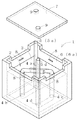
次に、本発明の好ましい実施形態を説明する。まず、図1に示す本発明に係るノイズフィルタ1の製造方法を説明する。前記製造方法は、磁性体形成ステップ、別途用意した導体を直線状から逆U字状に変形させる導体変形ステップと導体に抜け止め加工部を設ける抜け止め加工ステップ(なお、導体変形ステップと抜け止め加工ステップとをあわせて「導体成形ステップ」という。)、得られた磁性体に設けられた貫通孔に抜け止め加工済み逆U字状導体(以下、「加工済み導体」という。)を挿入する導体挿入ステップ、導体の先端部同士を電気的に接続する導体接続ステップ、及びケースと裏蓋を取り付けるパッケージステップからなる。以下、各ステップを順次説明する。
Next, a preferred embodiment of the present invention will be described. First, a method for manufacturing the
(磁性体形成ステップ)前記磁性体3として図2に示すような、直方体状をなす1個の塊状磁性体からなり、上面3aから底面3bに向かって4個の貫通孔4が垂直に形成されているとともに、前記上面3a又は前記底面3bから見ると前記貫通孔は縦2列、横2列となるように配置されている磁性体を用意する。前記磁性体3の材料は、Ni−Zn系フェライトであることが好ましい。
(Magnetic body forming step) As the
(導体形成ステップ:導体変形ステップ)別途用意した直線状の導体5を、図3に示すように、頂部5eが導体先端部5a(5c)及び5b(5d)側に対して直角になるようにプレス加工によって逆U字状に折り曲げて変形させ、逆U字状導体5fを得る。
(Conductor formation step: Conductor deformation step) As shown in FIG. 3, the separately prepared
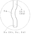
(導体形成ステップ:抜け止め加工ステップ)導体変形ステップにて得られた前記逆U字状導体5fの、前記先端部5a、5b、5c、5dと前記頂部5eとの間に、プレス加工によって、図4(a)に示す形状の抜け止め加工部5gを設け、加工済み導体5hを得る。前記抜け止め加工部5gの形状は、図4(a)に示す以外にも、図4(b)、図4(c)、図4(d)に示す形状のものを選択することができる。前記抜け止め加工部5gの幅又は直径は、前記貫通孔4の直径よりもわずかに大きくなるように設定される。なお、前記抜け止め加工部5gは、特に強調する場合を除いて、図面には表示しない。
(Conductor forming step: retaining process step) Between the
前記導体5は、Cu、Sn、Znから選択される1つの金属又はこれらの合金を使用する。また、導体5の断面の形状は、前記抜け止め加工部5g以外は円形であることが好ましいが、長方形であってもよい。前記金属を使用することにより、前記導体5は、抵抗値を下げてノイズ以外の電気信号が減衰されることを抑制する、表面の酸化を防止する、剛性を上げて壊れにくくする等の効果を得られる。
The
(導体挿入ステップ)図5に示すように、前記磁性体3の4個の貫通孔4のうち、隣り合う2個の貫通孔4a、4bに、上面3a側から加工済み導体5hの先端部5a、5bを挿入する。残る2つの貫通孔4c、4dにも、同様に上面3a側から加工済み導体5hの先端部5c、5dを挿入する。したがって、加工済み導体5hは、一部分が前記貫通孔4の内部に保持され、4個の先端部5a、5b、5c、5dが露出する。
(Conductor Insertion Step) As shown in FIG. 5, among the four through
(導体接続ステップ)図6に示すように、前記加工済み導体5hが挿入された前記磁性体3を、下面3bが上になるように図示しない台に載せ、前記先端部5a、5b、5c、5dのうち、2個の先端部5b、5cを、図7に示すように内側に折り曲げて接触させる。その後、はんだ付けやカシメ止め等の方法によって、前記先端部5b、5cを電気的に接続させる。このステップにより、インピーダンス素子2が完成する。すなわち、4本の貫通孔4を有する直方体状の磁性体3と、前記貫通孔4に挿通される2本の逆U字状の導体5とからなるとともに、前記導体5の先端部5b、5cを電気的に接続してなる1本の螺旋状内部コイルを有するインピーダンス素子2が完成する。
(Conductor Connection Step) As shown in FIG. 6, the
(パッケージステップ)図8に示すように、開口部6aを有する直方体状の樹脂製のケース6を用意し、前記開口部6aを上にして図示しない台の上に置き、前記インピーダンス素子2を前記磁性体3の下面3bが上になるようにして前記ケース6に収める。さらに、2個の貫通孔9を有する裏蓋7を、前記先端部5a、5dが前記貫通孔9を貫通するように前記開口部6aに設置し、係止め突起8により固定する。以上の方法により、再び図1に示す形状・構造を有するノイズフィルタ1が完成する。すなわち、4本の貫通孔4を有する直方体状の磁性体3と、前記貫通孔4に挿通される2本の逆U字状の導体5とからなるとともに、前記導体5の先端部5b、5cを電気的に接続してなる1本の螺旋状内部コイルを有するインピーダンス素子2と、そのインピーダンス素子2を1個内包する1組のケース6と裏蓋7とからなるノイズフィルタ1が完成する。これにより、前記磁性体3の上面3a側が、前記ケース6によって平らになり、前記ノイズフィルタ1は、一般的な実装装置によってノイズフィルタを実装する基板上に実装される。
(Packaging Step) As shown in FIG. 8, a rectangular
再び図7に示すように、導体5は、磁性体3の内部及び表面を巻回することにより螺旋状内部コイルを形成する。この構造によって、インピーダンス素子2及びそれを内包するノイズフィルタ1は、高いインダクタンス値を得られるため、高いノイズ除去性能を発揮できる。
As shown in FIG. 7 again, the
図9に示すように、先端部5a、5dは、外方に露出して外部接続用の端子となる。この構造によって、ノイズフィルタ1を設置する基板26と磁性体3との間に隙間が存在するため、基板26が変形したときに磁性体3が受ける応力を導体5が緩和して、磁性体3が破損しにくくなる。
As shown in FIG. 9, the tip portions 5a and 5d are exposed to the outside and serve as terminals for external connection. With this structure, there is a gap between the substrate 26 on which the
また、この構造により、基板26と導体5とが電気的に接続される。再び図14に示す従来のインピーダンス素子51の外部電極56の断面積よりも導体5の断面積の方が大きい場合、基板から磁性体3に至るまでの電気抵抗が下がり、インピーダンス素子2に大電流を流すことが可能になる。
Further, with this structure, the substrate 26 and the
再び図4(a)、図4(b)、図4(c)、図4(d)に示すように、導体5は、抜け止め加工部5gを有するため、導体5を磁性体3に固定することができ、貫通孔4の内部において振動することを抑制することができる。
As shown in FIGS. 4 (a), 4 (b), 4 (c), and 4 (d) again, since the
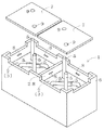
ここで、本発明の第二実施例は、図10に示すように、2個のインピーダンス素子2が、ケース6と裏蓋7との内部に収納されるとともに、インピーダンス素子2同士の間に非磁性体層28が存在する構造をとる。この構造によって、ディファレンシャルモードにおいて2個のインピーダンス素子2同士が磁束を打ち消し合うことを防止し、高いノイズ除去性能を発揮できる。
Here, in the second embodiment of the present invention, as shown in FIG. 10, two
ここで、本発明の他の実施形態を示す。(1)例えば、インピーダンス素子の製造方法において、磁性体成形ステップと導体成形ステップは独立しているため、先に導体形成ステップを行い、その後磁性体成型ステップを行うことができる。 Here, another embodiment of the present invention will be described. (1) For example, in the impedance element manufacturing method, since the magnetic body forming step and the conductor forming step are independent, the conductor forming step can be performed first, and then the magnetic body forming step can be performed.
(2)導体成形ステップにおいて、先に抜け止め加工ステップを行い、その後、導体変形ステップを行うことも可能である。 (2) In the conductor forming step, it is also possible to first perform a retaining step and then perform a conductor deformation step.
(3)加工済み導体5hの接続方法は、前記加工済み導体5hを折り曲げるのみならず、図11に示すように導体5と同じ材質からなり、両端に穴30を有する接続用金属片29を先端部5b、5cの間に橋渡しをした後に電気的に接続する方法、図12に示すように導体接続用回路31をと穴33とを有する接続基板32を、前記穴33に先端部5a、5b、5c、5dを挿通するように磁性体3の底面3bに載せ、前記導体接続用回路と導体5とを電気的に接続する方法等をとることができる。
(3) The processed
(4)また、接続された導体がなす螺旋状内部コイルの巻線方向は、図示しないが、必要に応じて右巻と左巻きを選択することができる。 (4) Although the winding direction of the spiral internal coil formed by the connected conductor is not shown, right-handed or left-handed can be selected as necessary.
(5)磁性体に設ける貫通孔及び逆U字状の導体の数は、貫通孔2本に対して導体を1本通す状態を1組と表現すれば、その状態を2組だけでなく必要なインダクタンス値を得られるように図13に示す3組の場合や、図示しないが4組以上に増やすことが可能である。 (5) The number of through-holes and inverted U-shaped conductors provided in the magnetic body is not limited to two sets if the state of passing one conductor through two through-holes is expressed as one set. In order to obtain a simple inductance value, it is possible to increase the number of sets to three or more as shown in FIG.
以上、本発明の詳細について、実施例を示しながら説明したが、ここで示したのは本発明の一実施形態であり、その技術思想を踏まえた上で、発明の効果を著しく損なわない程度において、前記実施形態の一部を変更して実施することが可能である。 The details of the present invention have been described above with reference to the examples. However, the present invention is only an embodiment of the present invention, and is based on the technical idea of the present invention without significantly impairing the effects of the invention. It is possible to carry out by changing a part of the embodiment.
本発明を利用すると、簡便かつ効率的に、ノイズ除去を必要とする電子機器の分野に対して、幅広く使用できるインピーダンス素子やノイズフィルタを提供できる。 By using the present invention, it is possible to provide an impedance element and a noise filter that can be widely used in the field of electronic devices that require noise removal simply and efficiently.
1:ノイズフィルタ
2:インピーダンス素子
3:磁性体
3a:上面
3b:底面
4、4a、4b、4c、4d:貫通孔
5:導体
5a、5b、5c、5d:先端部
5e:頂部
5f:逆U字状導体
5g:抜け止め加工部
5h:加工済み導体
6:ケース
6a:開口部
7:裏蓋
8:係止め部
9:貫通孔
26:基板
27:はんだ
28:非磁性体層
29:接続用金属片
30:穴
31:導体接続用回路
32:接続基板
33:穴
51:インピーダンス素子
52:磁性体
53:貫通孔
54:内部導電路
55:表面導電路
56:外部電極
1: Noise filter 2: Impedance element 3: Magnetic body 3a:
Claims (15)
A rectangular parallelepiped magnetic body having at least four even number of through-holes and an inverted U-shaped conductor inserted through the through-hole, and electrically connected at the tip of the conductor 1 It comprises an impedance element having a spiral internal coil, a pair of cases enclosing one or two impedance elements and a back cover, and the tip of the spiral internal coil is exposed to the outside of the back cover. Noise filter.
Priority Applications (1)
| Application Number | Priority Date | Filing Date | Title |
|---|---|---|---|
| JP2014011934A JP2015141902A (en) | 2014-01-27 | 2014-01-27 | Impedance element, method of manufacturing the same, noise filter using the same, and method of manufacturing the same |
Applications Claiming Priority (1)
| Application Number | Priority Date | Filing Date | Title |
|---|---|---|---|
| JP2014011934A JP2015141902A (en) | 2014-01-27 | 2014-01-27 | Impedance element, method of manufacturing the same, noise filter using the same, and method of manufacturing the same |
Publications (1)
| Publication Number | Publication Date |
|---|---|
| JP2015141902A true JP2015141902A (en) | 2015-08-03 |
Family
ID=53772117
Family Applications (1)
| Application Number | Title | Priority Date | Filing Date |
|---|---|---|---|
| JP2014011934A Pending JP2015141902A (en) | 2014-01-27 | 2014-01-27 | Impedance element, method of manufacturing the same, noise filter using the same, and method of manufacturing the same |
Country Status (1)
| Country | Link |
|---|---|
| JP (1) | JP2015141902A (en) |
Cited By (1)
| Publication number | Priority date | Publication date | Assignee | Title |
|---|---|---|---|---|
| CN115938790A (en) * | 2022-12-26 | 2023-04-07 | 广州市德珑电子器件有限公司 | Manufacturing method and structure of high-safety common-mode inductance magnetic ring |
Citations (8)
| Publication number | Priority date | Publication date | Assignee | Title |
|---|---|---|---|---|
| JPS5020152U (en) * | 1973-06-15 | 1975-03-07 | ||
| JPS5295326U (en) * | 1976-01-14 | 1977-07-16 | ||
| JPS56145122U (en) * | 1980-04-02 | 1981-11-02 | ||
| JPH0269909A (en) * | 1988-09-05 | 1990-03-08 | Matsushita Electric Ind Co Ltd | noise removal filter |
| JPH02120815U (en) * | 1989-03-16 | 1990-09-28 | ||
| JPH03124616U (en) * | 1990-03-29 | 1991-12-17 | ||
| JPH03286614A (en) * | 1990-04-02 | 1991-12-17 | Mitsubishi Electric Corp | Filter |
| JPH10270256A (en) * | 1997-03-21 | 1998-10-09 | Taiyo Yuden Co Ltd | Electronic part |
-
2014
- 2014-01-27 JP JP2014011934A patent/JP2015141902A/en active Pending
Patent Citations (8)
| Publication number | Priority date | Publication date | Assignee | Title |
|---|---|---|---|---|
| JPS5020152U (en) * | 1973-06-15 | 1975-03-07 | ||
| JPS5295326U (en) * | 1976-01-14 | 1977-07-16 | ||
| JPS56145122U (en) * | 1980-04-02 | 1981-11-02 | ||
| JPH0269909A (en) * | 1988-09-05 | 1990-03-08 | Matsushita Electric Ind Co Ltd | noise removal filter |
| JPH02120815U (en) * | 1989-03-16 | 1990-09-28 | ||
| JPH03124616U (en) * | 1990-03-29 | 1991-12-17 | ||
| JPH03286614A (en) * | 1990-04-02 | 1991-12-17 | Mitsubishi Electric Corp | Filter |
| JPH10270256A (en) * | 1997-03-21 | 1998-10-09 | Taiyo Yuden Co Ltd | Electronic part |
Cited By (1)
| Publication number | Priority date | Publication date | Assignee | Title |
|---|---|---|---|---|
| CN115938790A (en) * | 2022-12-26 | 2023-04-07 | 广州市德珑电子器件有限公司 | Manufacturing method and structure of high-safety common-mode inductance magnetic ring |
Similar Documents
| Publication | Publication Date | Title |
|---|---|---|
| US11587717B2 (en) | Inductor element | |
| CN201323122Y (en) | Electronic component | |
| US20040130428A1 (en) | Surface mount magnetic core winding structure | |
| US20140049353A1 (en) | Inductor and method of manufacturing inductor | |
| US10607769B2 (en) | Electronic component including a spacer part | |
| KR20160092674A (en) | Chip electronic component and board having the same mounted thereon | |
| US8878640B2 (en) | Common-mode choke coil | |
| JP2018186242A (en) | Coil parts and electronic equipment | |
| JP2005327876A (en) | Coil component and its manufacturing method | |
| US11908608B2 (en) | Coil component | |
| CN104051128A (en) | High Performance High Current Power Inductors | |
| CN113744951B (en) | Coil device | |
| KR20160014302A (en) | Chip electronic component and board having the same mounted thereon | |
| JP7288297B2 (en) | Coil parts and electronic equipment | |
| JP5217528B2 (en) | Multiple inductor | |
| CN110676015B (en) | Electronic device, connector and electromagnetic device thereof | |
| US20110122589A1 (en) | Magnetic element having improved transformers and commom mode chokes | |
| KR20140071756A (en) | Inductor and inductor manufacturing method | |
| KR20150139267A (en) | Wire wound inductor | |
| JP4666935B2 (en) | Toroidal choke parts | |
| JP2004266081A (en) | Common mode coil | |
| CN205016365U (en) | Inductor subassembly, DC -DC converter and high current output wave filter | |
| JP3165822U (en) | Winding chip choke coil | |
| US20190066904A1 (en) | Chip-type passive component | |
| JP5623330B2 (en) | Electronic components |
Legal Events
| Date | Code | Title | Description |
|---|---|---|---|
| A621 | Written request for application examination |
Free format text: JAPANESE INTERMEDIATE CODE: A621 Effective date: 20170123 |
|
| A977 | Report on retrieval |
Free format text: JAPANESE INTERMEDIATE CODE: A971007 Effective date: 20180118 |
|
| A131 | Notification of reasons for refusal |
Free format text: JAPANESE INTERMEDIATE CODE: A131 Effective date: 20180130 |
|
| A521 | Request for written amendment filed |
Free format text: JAPANESE INTERMEDIATE CODE: A523 Effective date: 20180330 |
|
| A131 | Notification of reasons for refusal |
Free format text: JAPANESE INTERMEDIATE CODE: A131 Effective date: 20180904 |
|
| A02 | Decision of refusal |
Free format text: JAPANESE INTERMEDIATE CODE: A02 Effective date: 20190312 |