JP2015152995A - Touch panel device - Google Patents
Touch panel device Download PDFInfo
- Publication number
- JP2015152995A JP2015152995A JP2014024140A JP2014024140A JP2015152995A JP 2015152995 A JP2015152995 A JP 2015152995A JP 2014024140 A JP2014024140 A JP 2014024140A JP 2014024140 A JP2014024140 A JP 2014024140A JP 2015152995 A JP2015152995 A JP 2015152995A
- Authority
- JP
- Japan
- Prior art keywords
- circuit
- touch
- touch panel
- electrode lines
- image area
- Prior art date
- Legal status (The legal status is an assumption and is not a legal conclusion. Google has not performed a legal analysis and makes no representation as to the accuracy of the status listed.)
- Granted
Links
Images


Landscapes
- Position Input By Displaying (AREA)
Abstract
Description
本発明は、静電容量方式のタッチパネル装置の入力方法および駆動方法に関するものである。 The present invention relates to an input method and a driving method of a capacitive touch panel device.
近年、入力デバイスの1つである静電容量方式のタッチパネルを液晶パネルや有機ELパネル等の表示パネルに貼り合せた表示装置が、2次元の座標入力手段として、パソコンや携帯情報端末の分野で広く普及している。 In recent years, a display device in which a capacitive touch panel, which is one of input devices, is bonded to a display panel such as a liquid crystal panel or an organic EL panel has been used as a two-dimensional coordinate input means in the field of personal computers and portable information terminals. Widely used.
このタッチパネル装置は、電極が配設された平板状をなすタッチパネル本体の表面側に、操作者の指などの指示物によるタッチ操作が行われるタッチ面が平面状に形成された2次元の座標入力手段である。 This touch panel device is a two-dimensional coordinate input in which a touch surface on which a touch operation is performed by an indicator such as an operator's finger is formed on the surface side of a flat touch panel body on which electrodes are arranged. Means.
静電容量方式のタッチパネルセンサー部分の配線は透明電極であるITO配線、あるいは銅配線が主流となっている。特許文献1では、銅または銅合金の網目状の銅配線で構成した電極線を形成することで表示部の画像を識別できるように銅配線の透明性を向上させている。この銅配線は大型化に適しているので50インチを越えた表示装置にも静電容量方式タッチパネルが実現可能になりつつある。
The wiring of the capacitive touch panel sensor part is mainly ITO wiring which is a transparent electrode or copper wiring. In
静電容量方式タッチパネル装置を備えた大型の表示装置の場合、大きな講堂やホールなどに設置されることが想定されるが、より多くの注目を集めるよう高い位置に設置するのが望ましい。しかし、表示画面が大きく、かつ高い位置に設置されると、表示部の表面をタッチ面にしても、全ての領域を操作者が指で触ることが難しい。その場合には大型の表示画面にタッチ操作を可能にするタッチパネル機能の有効性が失われてしまう問題があった。 In the case of a large display device provided with a capacitive touch panel device, it is assumed that it is installed in a large auditorium or hall, but it is desirable to install it at a high position to attract more attention. However, if the display screen is large and installed at a high position, it is difficult for the operator to touch the entire area with a finger even if the surface of the display unit is a touch surface. In that case, there is a problem that the effectiveness of the touch panel function that enables a touch operation on a large display screen is lost.
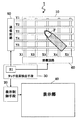
図11を参照してその問題の状況を説明する。図11では、静電容量方式タッチパネル装置を備えた大型の表示装置の画面に8個の押しボタンを表示している場合を示す。ここで操作者Mがタッチパネル本体10の3番のボタン位置3にタッチしようとしても、表示装置の画面が大きいために指が届かずにタッチ出来ない。
The problem situation will be described with reference to FIG. FIG. 11 shows a case where eight push buttons are displayed on the screen of a large display device having a capacitive touch panel device. Here, even if the operator M tries to touch the
また、小型のタッチパネル装置と同等のタッチ位置の分解精度や操作者Mの二本の指Fが近接したときの識別性能を求めると、大型の表示画面に重ね合わせたタッチパネル本体10の、タッチ位置検出用の電極線の本数が大幅に増加する問題があった。タッチ位置検出用の電極線の本数が大幅に増加すると、制御回路の信号線の本数や制御回路と接続するケーブルの信号線の本数などが増加することでタッチパネル装置のコストが大幅に増加してしまう問題があった。
Further, when the resolution accuracy of the touch position equivalent to that of the small touch panel device and the identification performance when the two fingers F of the operator M are close to each other are obtained, the touch position of the
本発明は 上記の問題を鑑みたものであり、縮小画像領域Sに表示画面全体に表示する画像を縮小して表示し、その縮小画像領域Sにタッチすることであたかも表示画面全体にタッチしているようにタッチ位置を示すカーソルを表示するものである。 The present invention has been made in view of the above-described problems. An image displayed on the entire display screen is reduced and displayed in the reduced image area S, and touching the reduced image area S is as if the entire display screen is touched. As shown, a cursor indicating the touch position is displayed.
また、上記の縮小画像領域S以外の表示画面でのタッチパネル装置の位置精度などの機能を必要最小限とし大幅なコストダウンを行なう。 In addition, functions such as the positional accuracy of the touch panel device on the display screen other than the reduced image area S described above are minimized, and the cost is greatly reduced.
本発明は、上記の課題を解決するために、互いに並走する複数の駆動信号電極線及び互いに並走する複数の信号検出電極線が格子状に配置されると共にその表面側に設けた保護絶縁体の表面をタッチ面にした平板状のタッチパネル本体を表示部に重ねて設けたタッチパネル装置であって、前記表示部へ表示する画像を制御する表示制御手段と、前記駆動信号電極線を順次に選択して駆動信号を印加する送信回路と、前記信号検出電極線を順次に選択して前記駆動信号電極線と前記信号検出電極線の交差点に形成される静電容量への蓄積電荷量を検出する受信回路と、前記送信回路と前記受信回路を制御することにより前記タッチ面への操作者のタッチ位置を検出するタッチ位置検出手段を備え、前記表示制御手段が、前記表示部の全体画面に表示する画像を縮小して該表示部の一部の縮小画像領域に表示する手段を有し、前記タッチ位置検出手段が、前記縮小画像領域へのタッチ位置と該縮小画像領域外へのタッチ位置を区別して検出する回路と、前記縮小画像領域へのタッチ位置の座標を全体画面の座標に拡大するタッチ位置座標変換回路を有し、前記表示制御手段が前記表示部に、前記タッチ位置を示すカーソルを前記全体画面の座標に表示したり、あたかも全体画面の対応する座標位置をタッチしたかのごとく操作されることを特徴とするタッチパネル装置である。 In order to solve the above-described problems, the present invention provides a protective insulation in which a plurality of drive signal electrode lines that run parallel to each other and a plurality of signal detection electrode lines that run parallel to each other are arranged in a lattice pattern and provided on the surface side thereof A touch panel device in which a flat touch panel body having a body surface as a touch surface is provided on a display unit, the display control means for controlling an image to be displayed on the display unit, and the drive signal electrode lines in order A transmission circuit that selects and applies a drive signal and the signal detection electrode line are sequentially selected to detect the amount of charge accumulated in the capacitance formed at the intersection of the drive signal electrode line and the signal detection electrode line And a touch position detection means for detecting the touch position of the operator on the touch surface by controlling the transmission circuit and the reception circuit, and the display control means is provided on the entire screen of the display unit. A means for reducing an image to be displayed and displaying it in a reduced image area as a part of the display unit, wherein the touch position detecting means includes a touch position on the reduced image area and a touch position outside the reduced image area. And a touch position coordinate conversion circuit for enlarging the coordinates of the touch position on the reduced image area to the coordinates of the entire screen, and the display control means displays the touch position on the display unit. The touch panel device is characterized in that a cursor is displayed on the coordinates of the whole screen or operated as if the corresponding coordinate position on the whole screen is touched.
本発明は、この構成により、縮小画像領域Sに表示画面全体を縮小した表示を設け、その部分をタッチすることで表示画面全体をあたかもタッチしているように表示することができる効果がある。 With this configuration, the present invention has an effect of providing a reduced display of the entire display screen in the reduced image area S and displaying the entire display screen as if touched by touching that portion.
また、本発明は、上記のタッチパネル装置であって、前記縮小画像領域の外側の駆動信号電極線及び信号検出電極線が、複数のノードを接続したノードを構成して該ノード毎に前記送信回路及び受信回路に接続されていることを特徴とするタッチパネル装置である。 The present invention is the above touch panel device, wherein the drive signal electrode line and the signal detection electrode line outside the reduced image area constitute a node connecting a plurality of nodes, and the transmission circuit is provided for each node. The touch panel device is connected to a receiving circuit.
本発明は、この構成により制御回路のコストを低減できる効果がある。 The present invention has an effect that the cost of the control circuit can be reduced by this configuration.
本発明は、大型の表示画面にタッチパネル本体を重ね合わせた静電容量式タッチパネル装置においても、縮小画像領域Sのタッチ面へのタッチ操作のタッチ位置検出の精度良くし、かつ、表示部の全画面の全体の位置と縮小画像領域Sへのタッチ位置をリンクさせることにより、画面全体に渡ってタッチ位置を移動することなくあたかも画面全体に対しタッチ操作をしているようにカーソルを表示させ画面全体を操作できる効果がある。 The present invention also improves the accuracy of the touch position detection of the touch operation on the touch surface of the reduced image area S and the entire display unit even in the capacitive touch panel device in which the touch panel body is superimposed on the large display screen. By linking the entire position of the screen and the touch position to the reduced image area S, the cursor is displayed as if the touch operation is performed on the entire screen without moving the touch position over the entire screen. There is an effect that the whole can be operated.
また、本発明は、縮小画像領域Sは従来と同等の位置精度や二本の指が近接したときの識別性能を確保し、縮小画像領域S以外では駆動信号電極線と信号検出電極線の本数を減らすことで制御回路のコストを大きく低減できる効果がある。 Further, according to the present invention, the reduced image area S has the same positional accuracy as the conventional one and the identification performance when two fingers are close to each other, and the number of drive signal electrode lines and signal detection electrode lines in the area other than the reduced image area S. As a result, the cost of the control circuit can be greatly reduced.
<第1の実施形態>
以下、図1から図12を参照して、本発明の第1の実施形態を説明する。図1は、第1の実施形態のタッチパネル装置1を示す全体構成図である。第1の実施形態の静電容量方式タッチパネル装置1は表示部40と、それに重ね合わせた平板状のタッチパネル本体10を備え、表示部40の表示を制御する表示制御手段20とタッチ位置検出手段30を備えている。
<First Embodiment>
Hereinafter, the first embodiment of the present invention will be described with reference to FIGS. FIG. 1 is an overall configuration diagram illustrating a
このタッチパネル装置1は、図1及び図2のように、表示部40に重ね合わせて設けたタッチパネル本体10の表面のタッチ面2に操作者Mの指Fを接触させて、その指Fのタッチ位置情報を取得する。
As shown in FIG. 1 and FIG. 2, the
タッチパネル本体10には、駆動信号電極線Y1〜Y5と、信号検出電極線(X1〜X5)を交差させて設ける。駆動信号電極線Y1〜Y5には、送信回路50から駆動信号(パルス信号)を印加する。そして、信号検出電極線(X1〜X5)には受信回路60を接続し、受信回路60が電極線の交差点に形成された静電容量の充放電電流信号を受信する。
The
タッチパネル装置1は、表示制御手段20が、タッチパネル本体10と重なる表示部40の表示を制御し、タッチ位置検出手段30が、相互容量方式で、送信回路50及び受信回路60の動作を制御して、受信回路60から出力される電極線の交差点の静電容量の蓄積電荷量の検出信号に基づいて操作者Mの指Fのタッチパネル装置1への接触位置の座標を計算する。
In the
(タッチパネル本体)
タッチパネル装置1のタッチパネル本体10は平板状であり、図4の様に、互いに並走する複数の駆動信号電極線(Y1〜Y5)と、互いに並走する複数の信号検出電極線(X1〜X5)とが格子状に交差して配置されている。
(Touch panel body)
The
図2は、図1に示したタッチパネル本体10の断面を示す模式的な断面図である。図2において電場の状況を破線で示す。なお、タッチパネル本体10は、数mm程度の厚さで構成することができるため、実際には、タッチパネル本体10は指Fに比較してかなり薄いものとなる。
FIG. 2 is a schematic cross-sectional view showing a cross section of the
タッチパネル本体10の表面の、操作者Mが指Fでタッチして操作するタッチ面2は、メラミン樹脂等の保護絶縁体11で形成し、その保護絶縁体11が駆動信号電極線Y1〜Y5を保護する。
The
タッチパネル本体10の駆動信号電極線Y1〜Y5と信号検出電極線X1〜X5は、PET(ポリエチレンテレフタレート)等の支持シート12によって支持し、支持シート12の表面側に駆動信号電極線Y1〜Y5を設け、支持シート12の裏面側に信号検出電極線X1〜X5を設ける。
The drive signal electrode lines Y1 to Y5 and the signal detection electrode lines X1 to X5 of the
駆動信号電極線Y1〜Y5と信号検出電極線X1〜X5とが支持シート12を挟んで重なり合う電極の交差点には静電容量C11、C12が形成される。その静電容量を経由して駆動信号電極線Y1〜Y5から信号検出電極線X1〜X5に電流が流れる。
Capacitances C11 and C12 are formed at intersections of electrodes where the drive signal electrode lines Y1 to Y5 and the signal detection electrode lines X1 to X5 overlap with the
図2のように操作者Mの指Fがタッチ面2の表面に接触すると、指F側を経由してグラウンドまで電流が流れることで、電極線の交差点の静電容量C11に流れる電流が減少することで、静電容量C11に蓄積する電荷が減る。受信回路60がこの電荷を測定し、タッチ位置検出手段30のタッチ位置検出回路31が、その電荷の減少量を計算することで、操作者Mの指Fがタッチした位置を検出する。
When the finger F of the operator M touches the surface of the
(タッチパネルの電極の配線)
以下では、後の図6のように、タッチパネル装置1の画面の左下に縮小画像領域Sを設けた例を説明する。しかし、縮小画像領域Sの全体画面における位置はそれに限定されず、全体画面のどの位置に設けても良い。
(Touch panel electrode wiring)
Hereinafter, an example in which the reduced image region S is provided in the lower left of the screen of the
大型の表示画面に合わせた静電容量式タッチパネル装置の通常の使用方法を鑑みると、縮小画像領域Sの外の領域では高い位置精度は求められないので、縮小画像領域S以外の表示画面でのタッチパネル装置の位置精度を定めるタッチパネル本体10の電極線の送信回路50及び受信回路60への配線を、以下のようにして、必要最小限に設定する。
In view of the normal usage of the capacitive touch panel device adapted to a large display screen, high positional accuracy is not required in the area outside the reduced image area S. The wiring of the electrode lines of the
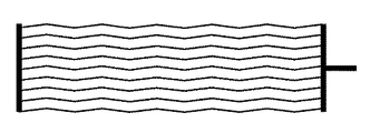
図3に、タッチパネルの駆動信号電極線Y及び信号検出電極線Xの電極線の配線の束の構成を示す。タッチパネルの駆動信号電極線Y又は信号検出電極線Xの1つのノードの電極線の構成は、図3のように、例えば5mmの幅に分散させて配置した9本の銅配線を束ねてその両端を接続して電極線を構成する。 FIG. 3 shows a configuration of a bundle of electrode lines of the drive signal electrode line Y and the signal detection electrode line X of the touch panel. The configuration of the electrode line of one node of the drive signal electrode line Y or the signal detection electrode line X of the touch panel is such that, as shown in FIG. 3, nine copper wires arranged in a 5 mm width, for example, are bundled and both ends thereof Are connected to form an electrode wire.
そして、図3の電極線で構成した駆動信号電極線Yと信号検出電極線Xを、タッチパネル本体10で、図4のように直角に交差させて格子状に電極線を配線する。図4では例として電極線のノードの5X5のマトリックスを示した。 Then, the drive signal electrode lines Y and the signal detection electrode lines X configured by the electrode lines in FIG. 3 are crossed at right angles as shown in FIG. FIG. 4 shows a 5 × 5 matrix of electrode line nodes as an example.
例えば寸法が縦747mm、横1329mm程度の大型の表示画面を持つタッチパネル装置1では、図5のように、1つのノード同士の交差する領域の寸法を、一般的なタッチパネル装置1の寸法と同様に5mmX5mmとして、60インチサイズ(16:9)で寸法が縦747mm、横1329mmのタッチパネル本体10を構成し、駆動信号電極線は約148本、信号検出電極線は約266本にする。
For example, in the
図6に駆動信号電極線と信号検出電極線の接続関係を示す。図6では、全体画面の左下の領域に縮小画像領域Sを設けた場合を示した。その縮小画像領域Sには、信号検出電極線X1〜X8と、駆動信号電極線Y144〜Y148を設定している。 FIG. 6 shows the connection relationship between the drive signal electrode lines and the signal detection electrode lines. FIG. 6 shows a case where the reduced image area S is provided in the lower left area of the entire screen. In the reduced image area S, signal detection electrode lines X1 to X8 and drive signal electrode lines Y144 to Y148 are set.
縮小画像領域Sの外の領域では、2本の電極線ノードを信号線の端で電気接続しそのまま制御回路へ入力する。すなわち、図6のように駆動信号電極線Y1とY2を電気接続し、信号検出電極線X9とX10を電気接続する。 In the area outside the reduced image area S, the two electrode line nodes are electrically connected at the end of the signal line and input to the control circuit as they are. That is, as shown in FIG. 6, the drive signal electrode lines Y1 and Y2 are electrically connected, and the signal detection electrode lines X9 and X10 are electrically connected.
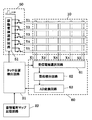
図7に、タッチパネル本体10に送信回路50と受信回路60を接続する回路のブロッ
ク図を示す。タッチパネル本体10の縮小画像領域Sの外の電極線の複数のノードを信号線の端で接続することで、その電極線が接続する制御部の回路のコストを低減できる。詳しくは、送信回路50と受信回路60の配線と回路を減らして回路のコストを低減でき、それらの回路を制御するタッチ位置検出回路31の配線と回路を減らして回路のコストを低減できる。
FIG. 7 shows a block diagram of a circuit for connecting the
また、縮小画像領域Sの外の電極線を、更に多数を、例えば3本のノードを信号線の端で接続して表示制御手段30のコストを更に低減することも可能である。この場合、精度が低下するので、精度が許容される限りで行う。 Further, it is possible to further reduce the cost of the display control means 30 by connecting more electrode lines outside the reduced image area S, for example, three nodes at the end of the signal line. In this case, the accuracy is lowered, so that the accuracy is allowed.
こうして、縮小画像領域Sでは、従来通りのタッチ位置検出精度と、近接した二本の指の接触位置の識別性能が得られる。一方、縮小画像領域Sの外の領域では、駆動信号電極線と信号検出電極線のノードを束ねることで、送信回路50と受信回路60と表示制御手段30の回路を減らす。それにより、タッチパネルの制御部のコストを低減することができる。
Thus, in the reduced image area S, the conventional touch position detection accuracy and the identification performance of the contact positions of two adjacent fingers can be obtained. On the other hand, in the area outside the reduced image area S, the nodes of the drive signal electrode line and the signal detection electrode line are bundled to reduce the circuits of the
(送信回路と受信回路)
図7のように、タッチ位置検出手段30のタッチ位置検出回路31が、送信回路50が駆動信号電極線Y1〜Y5に対して駆動信号を送信する動作を制御する。また、タッチ位置検出回路31が、受信回路60が信号検出電極線X1〜X5からの容量検出信号を受信する動作を制御する。それにより、受信回路60が、電極線の交点ごとの容量の蓄積電荷量を検出する。図8に、その送信回路50及び受信回路60の各部の信号の波形を示す。
(Transmission circuit and reception circuit)
As shown in FIG. 7, the touch
送信回路50は、駆動信号電極線Y1〜Y5ごとにスイッチング素子が接続されて構成される駆動電極選択回路51を有する。駆動電極選択回路51は、タッチ位置検出回路31に制御されて駆動信号電極線Y1〜Y5を1本ずつ選択して、図8(A)のように、パルス状の駆動信号を順次に駆動信号電極線Y1〜Y5に印加する。
The
受信回路60は、図7のように、受信電極選択回路61と電荷積分回路62とAD変換回路63とを備えている。受信電極選択回路61は、タッチ位置検出回路31に制御されて信号検出電極線X1〜X5を順に選択して、信号検出電極線X1〜X5からの出力信号を電荷積分回路62に順次入力させる。
As shown in FIG. 7, the receiving
図8(A)に示すように、受信電極選択回路61は、駆動電極選択回路51に選択された駆動信号電極線Y1〜Y5の1つ毎に、信号検出電極線X1〜X5を1本ずつ順次に選択して信号検出電極線X1〜X5の充放電電流信号を電荷積分回路62に送信する。これにより、全ての駆動信号電極線Y1〜Y5と全ての信号検出電極線X1〜X5の全ての組み合わせにおける充放電電流信号を読み出すことで、全ての電極線の交点ごとの充放電電流信号を取り出すことができる。
As shown in FIG. 8A, the reception
電荷積分回路62は、受信電極選択回路61から入力された、信号検出電極線X1〜X5の充放電電流信号(アナログ信号)を時間積分して電極線の交点ごとの容量の蓄積電荷量をあらわす電圧信号に変換し、その電圧信号をAD変換回路63に送信する。AD変換回路63は、その電圧信号をディジタルデータであらわしたディジタル信号に変換して出力する。
The
図8(B)のように、駆動信号電極線Y1〜Y5に駆動信号(パルス信号)を印加すると、電荷積分回路62の出力のピークが所定の振幅で変化するが、操作者Mの指Fがその電極線の交差点にタッチすると、操作者の指Fが導電性を持っておりグラウンド接地として働く。それにより、指と駆動信号電極線Y、指Fと信号検出電極線Xとの間の電気力線
に変化が生じ、図12のように、電荷積分回路62の出力電圧が小さくなる。
As shown in FIG. 8B, when a drive signal (pulse signal) is applied to the drive signal electrode lines Y1 to Y5, the peak of the output of the
(制御部)
図9は、タッチパネル装置1の制御部の回路のブロック図を示す。この制御部は、図9のように、表示制御手段20とタッチ位置検出手段30と送信回路50と受信回路60で構成する。
(Control part)
FIG. 9 is a block diagram of a circuit of the control unit of the
(表示制御手段)
表示制御手段20は、表示すべき画像データを作成する画像データ作成回路21と、画像データ作成回路21が作成した画像を縮小して縮小画像領域Sに表示する画像データを作成する画像データ縮小回路22と、縮小画像領域S用に縮小された画像データを、画像データ作成回路21が作成した元の画像データと合成した合成画像データを作成する画像データ合成回路23を有する。
(Display control means)
The display control means 20 includes an image
また、操作者Mの指Fのタッチ面2への接触位置のデータをタッチ位置検出手段30から受信して、画像データ作成回路21に、カーソルの画像を加えた画像データを作成させる制御を行うカーソル画像追加回路24を有する。
In addition, the operator M receives the touch position data of the finger F on the
(タッチ位置検出手段)
タッチ位置検出手段30は、タッチ位置検出回路31と、蓄積電荷マップ記憶回路32と、縮小画面/全体画面判定回路33と、タッチ位置座標変換回路34を有する。
(Touch position detection means)
The touch
タッチ位置検出回路31は、送信回路50を制御して、送信回路50に駆動信号電極線Y1〜Y5を順次に選択させて、図8(A)のように駆動信号電極線Y1〜Y5にパルス状の駆動信号を印加させる。また、受信回路60を制御して、受信回路60に信号検出電極線X1〜X5を順次に選択させて、信号検出電極線X1〜X5からの信号を取り出させる制御を行う。
The touch
そうして、受信回路60が、電極線の交差点の各静電容量に蓄積された電荷量を測定し、その値のディジタルデータを作成してタッチ位置検出回路に送信する。
Then, the receiving
蓄積電荷マップ記憶回路32は、操作者Mの指が接触しない状態の電極線の交差点の静電容量に蓄積される電荷の量を記憶する。
The accumulated charge
タッチ位置検出回路31は、受信回路60から受信した電極線の交差点の静電容量の電荷の量と蓄積電荷マップ記憶回路32が記憶する電荷の量の差を計算し、その差の大きさによって、操作者Mの指Fのタッチ位置を検出する。
The touch
縮小画面/全体画面判定回路33は、タッチ位置が縮小画像領域Sの位置か、それ以外の全体画面の位置かを判定する。
The reduced screen / whole
タッチ位置座標変換回路34は、縮小画面/全体画面判定回路33の判定結果に基づき、画面に表示するカーソルの位置座標を計算してその位置座標のデータをカーソル画像追加回路24に送信する。
The touch position coordinate
(動作手順)
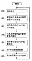
以下で、本実施形態の静電容量方式タッチパネル装置1の動作を、図10のフローチャートと、図11と図12を参照して説明する。
(Operation procedure)
Hereinafter, the operation of the capacitive
(ステップS1)画面表示処理
図10のステップS1の画面表示処理では、図11のように、表示制御手段20が、タッチパネル装置1の大型の表示部40の画面に、例えば8個の押しボタンを表示する。ここで、表示制御手段20は、表示部40の全体に表示する画像を縮小して、その縮小画像を縮小画像領域Sに表示する。
(Step S1) Screen Display Processing In the screen display processing in step S1 of FIG. 10, the display control means 20 applies, for example, eight push buttons on the screen of the
操作者MはステップS3で、タッチパネル本体10のタッチ面2に指Fを接触して画面を操作する。その操作者Mの指Fのタッチ面2への接触位置をタッチ位置検出手段30が検出する。
In step S3, the operator M touches the
表示制御手段20の動作の詳細は、表示制御手段20の画像データ作成回路21が、カーソル画像追加回路24から操作者Mの指Fが接触した位置のカーソル位置のデータを受信して、全体の画面に表示する画像データを作成する。次に、画像データ縮小回路22が、画像データ作成回路21が発生させた画面を縮小した画像データを作成する。
The details of the operation of the display control means 20 are as follows. The image
次に、画像データ合成回路23が、画像データ縮小回路22が縮小した画像データを、画像データ作成回路21が作成した画像データと合成した合成画像データを作成する。そして、合成画像データを表示部40が表示する。
Next, the image
(ステップS2)電極線の交差点の静電容量への充放電処理
タッチ位置検出手段30のタッチ位置検出回路31が、タッチパネル本体10の電極に接続した送信回路50を制御して、駆動信号電極線(Y1〜Y5)を順次に選択して駆動信号を印加し、また、受信回路60を制御して、信号検出電極線(X1〜X5)を順次に選択して電極線の交差点の静電容量の例えばC12の充放電電流を検出する。
(Step S2) Charge / Discharge Processing for Capacitances at Intersections of Electrode Lines The touch
(ステップS3)操作者の指のタッチ面への接触操作
操作者Mは、タッチパネル本体10の3番のボタン位置3をタッチしようとする場合に、全体画面が大きいために指Fが3番のボタン位置3には届かない。操作者Mは、その3番のボタン位置3の替りに、図11の様に、画面の左下位置に設けた縮小画像領域Sに表示されている3番のボタン位置3sにタッチする。
(Step S3) When the operator M is going to touch the
(ステップS4)交差点静電容量の蓄積電荷の検出処理
図2のように、操作者Mの指Fが、タッチパネル本体10の電極線の交差点の静電容量C11の位置のタッチ面2に接触すると、電極線の交差点の電界が変化することで電極線の交差点の静電容量静電容量C11に流れる電流が減少し、その静電容量C11に蓄積される電荷量が減少する。すなわち、タッチパネル本体10のタッチ面2に対する操作者の指Fによるタッチ操作に応じて、格子状の駆動信号電極線(Y1〜Y5)と信号検出電極線(X1〜X5)の交差点の静電容量に流れる電流が変化する。
(Step S4) Processing for Detecting Accumulated Charge at Intersection Capacitance As shown in FIG. When the electric field at the intersection of the electrode lines changes, the current flowing through the electrostatic capacitance C11 at the intersection of the electrode lines decreases, and the amount of charge accumulated in the electrostatic capacitance C11 decreases. That is, according to the touch operation of the
受信回路60は、駆動信号電極線に印加された駆動信号に応答した信号検出電極線(X1〜X5)の電極に流れる静電容量C11の充放電電流信号を受信する。すなわち、受信回路60は、駆動信号電極線Y1〜Y5と信号検出電極線X1〜X5とが交差する電極線の交差点ごとの静電容量C11、C12等に蓄積される電荷量による電流を測定して、その電流を積分することで電極線の交差点ごとの蓄積電荷の値を検出する。
The receiving
図12は、図1に示したタッチ面2に対するタッチ操作の位置に応じて受信回路60の電荷積分回路62から出力される信号を示す図である。駆動信号電極線Y1〜Y5及び信号検出電極線X1〜X5の選択により電極線の交差点ごとに信号検出電極線X1〜X5から出力される信号が電荷積分回路62によって時間積分されて交差点の静電容量の蓄積電荷量をあらわす電圧信号が得られる。
FIG. 12 is a diagram illustrating a signal output from the
図12(A)のように、タッチ面2における駆動信号電極線Y1と信号検出電極線X4との電極線の交差点上にタッチした場合は、駆動信号電極線Y1と信号検出電極線X4との電極線の交差点(X4,Y1)の静電容量に蓄積される電荷量が減少する。そのため、図12(B)のように、電荷積分回路62が駆動信号電極線Y1と信号検出電極線X4の交差点の静電容量に蓄積される電荷の充放電電流を検出して時間積分して電圧値を得る場合に、その電圧信号のレベルが低下する。
As shown in FIG. 12A, when touching the intersection of the drive signal electrode line Y1 and the signal detection electrode line X4 on the
それ以外に、電極線の交差点(X3,Y1)と(X5,Y1)、及び、(X3,Y2)と(X4,Y2)と(X5,Y2)の静電容量に蓄積される電荷量も少し減少して電荷積分回路62の出力電圧信号のレベルが少し低下する。
In addition, the amount of charge accumulated in the capacitances of the intersections (X3, Y1) and (X5, Y1) and (X3, Y2), (X4, Y2) and (X5, Y2) of the electrode lines The level of the output voltage signal of the
その交差点の静電容量の蓄積電荷量をあらわす電圧信号のレベルをAD変換回路63がディジタルデータに変換してタッチ位置検出手段30のタッチ位置検出回路31に出力する。
The
(ステップS5)タッチ位置検出処理
タッチ位置検出手段30のタッチ位置検出回路31が、受信回路60のAD変換回路63から、電極線の交差点の静電容量C11に蓄積された電荷量のディジタルデータを受信する。そして、その電荷量と蓄積電荷マップ記憶回路32の記憶している電荷量の値との差を計算し、その値の差が大きい場合に、その電極線の交差点に操作者の指Fが接触していると判定する。
(Step S5) Touch Position Detection Processing The touch
図12の場合では、電極線の交差点の静電容量に蓄積される電荷量の減少幅は、電極線の交差点(X4,Y1)が最も大きい。そのため、タッチ位置検出回路31は、出力値の低下がもっとも大きい電極線の交差点(X4,Y1)をタッチ位置であると判定する。
In the case of FIG. 12, the amount of decrease in the amount of charge accumulated in the capacitance at the intersection of the electrode lines is the largest at the intersection (X4, Y1) of the electrode lines. For this reason, the touch
こうして、タッチ位置検出手段30のタッチ位置検出回路31が、送信回路50を制御して受信回路60が検出した信号検出電極線(X1〜X5)の電極の出力信号の変化に基づいて操作者の指Fのタッチ面2への接触位置を検出する。
In this way, the touch
(ステップS6)タッチ位置座標変換処理
縮小画面/全体画面判定回路33が、タッチ位置検出回路31の検出したタッチ位置座標を、縮小画像領域S内にある位置座標か、それ以外の領域にある位置座標であるかを判定する。
(Step S6) Touch Position Coordinate Conversion Process The touch position coordinates detected by the reduced screen / whole
図11の例では、縮小画面/全体画面判定回路33が、検出された3番のボタン位置3sのタッチ位置座標が縮小画像領域S内にあると判定する。タッチ位置座標が縮小画像領域S内にあるので、タッチ位置座標変換回路34が、その座標を全体画面の位置座標へ変換し、それにより、元の画面にある3番のボタン位置3がタッチされたものとする。
In the example of FIG. 11, the reduced screen / whole
次に、タッチ位置座標変換回路34が、その判定結果に基づき、位置座標が縮小画像領域S内にあった場合、全体画面の位置座標へ変換する位置座標変換処理を行う。また、タッチ位置座標変換回路34は、位置座標が縮小画像領域S内に無い場合は、そのままの座標を位置座標とする。
Next, based on the determination result, the touch position coordinate
(ステップS7)タッチ位置カーソル表示処理
次に、表示制御手段20のカーソル画像追加回路24が、タッチ位置座標変換回路34が計算した位置座標データを用いて、タッチ位置のカーソルを全体画面に表示させる画像処理を行なう。
(Step S7) Touch Position Cursor Display Processing Next, the cursor
これにより、表示制御手段20が、縮小画像領域S内のタッチ部分に対応する部分のカーソルを、画面全体に対応させた位置に表示する。こうして、タッチパネル装置1が、操作者Mがあたかも表示画面全体の位置に自由に接触しているような様子で、表示部40の全画面内を動くカーソルを表示する。
Thereby, the display control means 20 displays the cursor of the part corresponding to the touch part in the reduced image area S at the position corresponding to the entire screen. In this way, the
このように、大型の表示画面に合わせた静電容量式タッチパネル装置1において、縮小画像領域Sを画面全体の位置とリンクさせることにより、操作者Mが縮小画像領域S内に指Fを接触させるだけで、タッチ位置を示すカーソルを表示部40の全体画面の広い領域内を移動させて、全体画面に対するタッチ位置を指定するマンマシンインターフェースを備えたタッチパネル装置1を実現することができる。
In this way, in the capacitive
1・・・タッチパネル装置
2・・・タッチ面
3・・・ボタン位置
3s・・・ボタン位置
10・・・タッチパネル本体
11・・・保護絶縁体
12・・・支持シート
20・・・表示制御手段
21・・・画像データ作成回路
22・・・画像データ縮小回路
23・・・画像データ合成回路
24・・・カーソル画像追加回路
30・・・タッチ位置検出手段
31・・・タッチ位置検出回路
32・・・蓄積電荷マップ記憶回路
33・・・縮小画面/全体画面判定回路
34・・・タッチ位置座標変換回路
40・・・表示部
50・・・送信回路
51・・・駆動電極選択回路
60・・・受信回路
61・・・受信電極選択回路
62・・・電荷積分回路
63・・・AD変換回路
C11、C12・・・静電容量
F・・・操作者の指
M・・・操作者
S・・・縮小画像領域
X1〜X5・・・信号検出電極線
Y1〜Y5・・・駆動信号電極線
DESCRIPTION OF
Claims (2)
前記表示部へ表示する画像を制御する表示制御手段と、前記駆動信号電極線を順次に選択して駆動信号を印加する送信回路と、前記信号検出電極線を順次に選択して前記駆動信号電極線と前記信号検出電極線の交差点に形成される静電容量への蓄積電荷量を検出する受信回路と、前記送信回路と前記受信回路を制御することにより前記タッチ面への操作者のタッチ位置を検出するタッチ位置検出手段を備え、
前記表示制御手段が、前記表示部の全体画面に表示する画像を縮小して該表示部の一部の縮小画像領域に表示する手段を有し、
前記タッチ位置検出手段が、前記縮小画像領域へのタッチ位置と該縮小画像領域外へのタッチ位置を区別して検出する回路と、前記縮小画像領域へのタッチ位置の座標を全体画面の座標に拡大するタッチ位置座標変換回路を有し、
前記表示制御手段が前記表示部に、前記タッチ位置を示すカーソルを前記全体画面の座標に表示したり、あたかも全体画面の対応する座標位置をタッチしたかのごとく操作されることを特徴とするタッチパネル装置。 A flat touch panel body in which a plurality of drive signal electrode lines running parallel to each other and a plurality of signal detection electrode lines running parallel to each other are arranged in a grid and the surface of the protective insulator provided on the surface side is the touch surface Is a touch panel device provided on the display unit,
Display control means for controlling an image displayed on the display unit, a transmission circuit for sequentially selecting the drive signal electrode lines and applying a drive signal, and the drive signal electrodes by sequentially selecting the signal detection electrode lines A receiving circuit that detects the amount of charge accumulated in the capacitance formed at the intersection of the line and the signal detection electrode line, and the touch position of the operator on the touch surface by controlling the transmitting circuit and the receiving circuit Touch position detecting means for detecting
The display control means includes means for reducing an image to be displayed on the entire screen of the display unit and displaying the reduced image on a part of the reduced image area of the display unit;
The touch position detecting means detects the touch position to the reduced image area and the touch position outside the reduced image area, and expands the coordinates of the touch position to the reduced image area to the coordinates of the entire screen. Touch position coordinate conversion circuit,
The touch panel, wherein the display control unit is operated as if the cursor indicating the touch position is displayed on the coordinates of the whole screen on the display unit, or as if the corresponding coordinate position of the whole screen is touched. apparatus.
Priority Applications (1)
| Application Number | Priority Date | Filing Date | Title |
|---|---|---|---|
| JP2014024140A JP6287297B2 (en) | 2014-02-12 | 2014-02-12 | Touch panel device |
Applications Claiming Priority (1)
| Application Number | Priority Date | Filing Date | Title |
|---|---|---|---|
| JP2014024140A JP6287297B2 (en) | 2014-02-12 | 2014-02-12 | Touch panel device |
Publications (2)
| Publication Number | Publication Date |
|---|---|
| JP2015152995A true JP2015152995A (en) | 2015-08-24 |
| JP6287297B2 JP6287297B2 (en) | 2018-03-07 |
Family
ID=53895214
Family Applications (1)
| Application Number | Title | Priority Date | Filing Date |
|---|---|---|---|
| JP2014024140A Active JP6287297B2 (en) | 2014-02-12 | 2014-02-12 | Touch panel device |
Country Status (1)
| Country | Link |
|---|---|
| JP (1) | JP6287297B2 (en) |
Cited By (3)
| Publication number | Priority date | Publication date | Assignee | Title |
|---|---|---|---|---|
| JP2018005291A (en) * | 2016-06-27 | 2018-01-11 | 株式会社ジャパンディスプレイ | Display device |
| JP2020091487A (en) * | 2016-07-11 | 2020-06-11 | 株式会社ジャパンディスプレイ | Detection device and display device |
| US11036332B2 (en) | 2016-07-11 | 2021-06-15 | Japan Display Inc. | Cover member and display apparatus |
Citations (6)
| Publication number | Priority date | Publication date | Assignee | Title |
|---|---|---|---|---|
| JPH11259237A (en) * | 1998-03-12 | 1999-09-24 | Ricoh Co Ltd | Image display device |
| JP2009064209A (en) * | 2007-09-06 | 2009-03-26 | Sharp Corp | Information display device |
| JP2010039515A (en) * | 2008-07-31 | 2010-02-18 | Dmc:Kk | Touch panel |
| WO2012173068A1 (en) * | 2011-06-15 | 2012-12-20 | シャープ株式会社 | Touch panel |
| JP2013097801A (en) * | 2011-10-28 | 2013-05-20 | Eturbotouch Technology Inc | Touch panel |
| JP2014178791A (en) * | 2013-03-14 | 2014-09-25 | Ricoh Co Ltd | Projector, projection system, image generation program, and image generation method |
-
2014
- 2014-02-12 JP JP2014024140A patent/JP6287297B2/en active Active
Patent Citations (6)
| Publication number | Priority date | Publication date | Assignee | Title |
|---|---|---|---|---|
| JPH11259237A (en) * | 1998-03-12 | 1999-09-24 | Ricoh Co Ltd | Image display device |
| JP2009064209A (en) * | 2007-09-06 | 2009-03-26 | Sharp Corp | Information display device |
| JP2010039515A (en) * | 2008-07-31 | 2010-02-18 | Dmc:Kk | Touch panel |
| WO2012173068A1 (en) * | 2011-06-15 | 2012-12-20 | シャープ株式会社 | Touch panel |
| JP2013097801A (en) * | 2011-10-28 | 2013-05-20 | Eturbotouch Technology Inc | Touch panel |
| JP2014178791A (en) * | 2013-03-14 | 2014-09-25 | Ricoh Co Ltd | Projector, projection system, image generation program, and image generation method |
Cited By (4)
| Publication number | Priority date | Publication date | Assignee | Title |
|---|---|---|---|---|
| JP2018005291A (en) * | 2016-06-27 | 2018-01-11 | 株式会社ジャパンディスプレイ | Display device |
| US10860830B2 (en) | 2016-06-27 | 2020-12-08 | Japan Display Inc. | Display device |
| JP2020091487A (en) * | 2016-07-11 | 2020-06-11 | 株式会社ジャパンディスプレイ | Detection device and display device |
| US11036332B2 (en) | 2016-07-11 | 2021-06-15 | Japan Display Inc. | Cover member and display apparatus |
Also Published As
| Publication number | Publication date |
|---|---|
| JP6287297B2 (en) | 2018-03-07 |
Similar Documents
| Publication | Publication Date | Title |
|---|---|---|
| US8970527B2 (en) | Capacitive touch panel having mutual capacitance and self capacitance sensing modes and sensing method thereof | |
| JP4670970B2 (en) | Display input device | |
| JP4932667B2 (en) | Screen input type image display system | |
| JP5264800B2 (en) | Touch panel device | |
| CN107783689B (en) | Driver chip, circuit film, chip-on-film type driver circuit, and display device | |
| JP2009122969A (en) | Screen input type image display device | |
| CN103941914B (en) | Touch panel, touch display panel and sensing method of touch signal | |
| JP2010055612A (en) | Multi-point touch-sensitive system | |
| KR101394731B1 (en) | Electronic device | |
| TW201237681A (en) | Position-sensing and force detection panel | |
| JP2010055613A (en) | Operation method for multi-point touch-sensitive system | |
| US20130321290A1 (en) | Method and apparatus for sensing touch input | |
| CN102289316A (en) | Method and apparatus for correcting touch coordinates in touch system | |
| JP2013517559A (en) | 5-wire resistive touch screen pressure measurement circuit and method | |
| CN101661362A (en) | Multipoint touch sensing device | |
| JP6578010B2 (en) | Method for correcting sensitivity of touch input device for detecting touch pressure and computer-readable recording medium | |
| KR101859713B1 (en) | The touch input device for providing user interface and the method for the same | |
| JP6287297B2 (en) | Touch panel device | |
| TWI545467B (en) | Detecting sensor, indicator position detecting device, and method for manufacturing detecting sensor | |
| EP2494429B1 (en) | Method and device for providing a touch screen with equi-potential connection points | |
| JP2015111317A (en) | Portable device with touch sensor and display device | |
| CN102193694A (en) | Electronics for Compensating Capacitance Deviations | |
| JP2013206341A (en) | Touch panel, touch panel controller, and information processor | |
| KR20150062714A (en) | Touchscreen apparatus | |
| CN104035638A (en) | Touch electrode structure, touch panel, display device and method for positioning touch point |
Legal Events
| Date | Code | Title | Description |
|---|---|---|---|
| A621 | Written request for application examination |
Free format text: JAPANESE INTERMEDIATE CODE: A621 Effective date: 20170119 |
|
| A131 | Notification of reasons for refusal |
Free format text: JAPANESE INTERMEDIATE CODE: A131 Effective date: 20170926 |
|
| A521 | Request for written amendment filed |
Free format text: JAPANESE INTERMEDIATE CODE: A523 Effective date: 20171109 |
|
| TRDD | Decision of grant or rejection written | ||
| A01 | Written decision to grant a patent or to grant a registration (utility model) |
Free format text: JAPANESE INTERMEDIATE CODE: A01 Effective date: 20180109 |
|
| A61 | First payment of annual fees (during grant procedure) |
Free format text: JAPANESE INTERMEDIATE CODE: A61 Effective date: 20180122 |
|
| R150 | Certificate of patent or registration of utility model |
Ref document number: 6287297 Country of ref document: JP Free format text: JAPANESE INTERMEDIATE CODE: R150 |
|
| R250 | Receipt of annual fees |
Free format text: JAPANESE INTERMEDIATE CODE: R250 |
|
| R250 | Receipt of annual fees |
Free format text: JAPANESE INTERMEDIATE CODE: R250 |
|
| R250 | Receipt of annual fees |
Free format text: JAPANESE INTERMEDIATE CODE: R250 |
|
| R250 | Receipt of annual fees |
Free format text: JAPANESE INTERMEDIATE CODE: R250 |
|
| R250 | Receipt of annual fees |
Free format text: JAPANESE INTERMEDIATE CODE: R250 |
|
| R250 | Receipt of annual fees |
Free format text: JAPANESE INTERMEDIATE CODE: R250 |