JP2015180902A - LASER DEVICE, EXPOSURE DEVICE AND INSPECTION DEVICE EQUIPPED WITH THIS LASER DEVICE - Google Patents
LASER DEVICE, EXPOSURE DEVICE AND INSPECTION DEVICE EQUIPPED WITH THIS LASER DEVICE Download PDFInfo
- Publication number
- JP2015180902A JP2015180902A JP2012169643A JP2012169643A JP2015180902A JP 2015180902 A JP2015180902 A JP 2015180902A JP 2012169643 A JP2012169643 A JP 2012169643A JP 2012169643 A JP2012169643 A JP 2012169643A JP 2015180902 A JP2015180902 A JP 2015180902A
- Authority
- JP
- Japan
- Prior art keywords
- light
- wavelength
- laser
- converted
- optical element
- Prior art date
- Legal status (The legal status is an assumption and is not a legal conclusion. Google has not performed a legal analysis and makes no representation as to the accuracy of the status listed.)
- Pending
Links
Images



Landscapes
- Optical Modulation, Optical Deflection, Nonlinear Optics, Optical Demodulation, Optical Logic Elements (AREA)
- Exposure Of Semiconductors, Excluding Electron Or Ion Beam Exposure (AREA)
- Exposure And Positioning Against Photoresist Photosensitive Materials (AREA)
Abstract
Description
本発明は、レーザ光を発生するレーザ光発生部と、レーザ光を増幅する増幅部と、増幅されたレーザ光を波長変換する波長変換部とを備えたレーザ装置に関する。また、このようなレーザ装置を備えた露光装置及び検査装置等のレーザシステムに関する。 The present invention relates to a laser device including a laser light generation unit that generates laser light, an amplification unit that amplifies the laser light, and a wavelength conversion unit that converts the wavelength of the amplified laser light. The present invention also relates to a laser system such as an exposure apparatus and an inspection apparatus provided with such a laser apparatus.
上記のようなレーザ装置は、例えば顕微鏡や形状測定装置、露光装置、検査装置などのレーザシステムの光源として用いられている。レーザ装置の出力波長は、組み込まれるシステムの用途及び機能に応じて設定され、例えば、出力光の波長が193nm,266nm,355nm等のレーザ装置が知られている。レーザ光発生部で発生するレーザ光(シード光)の波長や、増幅部に設ける増幅器の列数及び段数、波長変換部に設ける波長変換光学素子の種別及び組み合わせは、レーザシステムの用途や機能等に応じて設定される(例えば、特許文献1を参照)。 The laser apparatus as described above is used as a light source of a laser system such as a microscope, a shape measuring apparatus, an exposure apparatus, and an inspection apparatus. The output wavelength of the laser device is set in accordance with the use and function of the system to be incorporated. For example, laser devices having output light wavelengths of 193 nm, 266 nm, 355 nm, and the like are known. The wavelength of the laser light (seed light) generated by the laser light generation unit, the number of columns and stages of amplifiers provided in the amplification unit, the type and combination of wavelength conversion optical elements provided in the wavelength conversion unit, and the use and function of the laser system (For example, refer to Patent Document 1).
このようなレーザ装置において、出力光を高速でオン/オフするために幾つかの手法が提案されている。例えば、第1の技術では、波長変換光学系を複数の並列光路(例えば第1系列及び第2系列等)とこれらの並列光路から出射した光が重ね合わされて入射する直列光路とから構成し、各並列光路に対応して光源及び増幅器を設ける。第1系列及び第2系列には各光源から出射し各々増幅器により増幅されたパルス光を入射させておき、各光源の発光タイミングを調整する。すなわち、直列経路の最終段の波長変換光学素子における第1系列を通ったパルス光と第2系列を通ったパルス光との時間的な重ね合わせを制御し、これにより出力光をオン/オフ制御する(例えば、特許文献2を参照)。 In such a laser apparatus, several methods have been proposed to turn on / off output light at high speed. For example, in the first technique, the wavelength conversion optical system is configured by a plurality of parallel optical paths (for example, the first series and the second series, etc.) and a series optical path on which light emitted from these parallel optical paths is superimposed and incident, A light source and an amplifier are provided corresponding to each parallel optical path. Pulse light emitted from each light source and amplified by an amplifier is incident on the first series and the second series, and the light emission timing of each light source is adjusted. That is, the temporal superposition of the pulsed light passing through the first series and the pulsed light passing through the second series in the wavelength conversion optical element at the final stage of the series path is controlled, thereby controlling the output light on / off. (For example, refer to Patent Document 2).
また、第2の技術では、波長変換光学系を複数の波長変換光学素子からなる単一の直列光路とし、一組の光源及び増幅器で構成する。そして、光源から出射するシード光をピークパワーが高い状態と低い状態とに切り換え、これにより波長変換効率を変化させて出力光をオン/オフ制御する。 In the second technique, the wavelength conversion optical system is a single serial optical path composed of a plurality of wavelength conversion optical elements, and is configured by a set of light sources and amplifiers. Then, the seed light emitted from the light source is switched between a state where the peak power is high and a state where the peak power is low, thereby changing the wavelength conversion efficiency and controlling the output light on / off.
確かに、第1の技術においては、レーザ装置を構成する各光源、各増幅器,及び最終段の波長変換光学素子を除く全波長変換光学素子が常に動作状態ないし波長変換状態になるため、熱的に安定であり、出力光を高速且つ安定的にオン/オフ制御することができる。しかしながら、例えば波長1065nmの単一の光源の第3高調波により波長355nmの光を発生させるような単純な系ではこの方法は適用できない。また、波長変換光学系を形成する並列回路の数に応じて光源及び増幅器が必要であり、レーザ装置の構成が複雑化するという課題があった。 Certainly, in the first technique, all the wavelength conversion optical elements except for the respective light sources, amplifiers, and final stage wavelength conversion optical elements constituting the laser device are always in an operating state or a wavelength conversion state. Therefore, the output light can be controlled on / off stably at high speed. However, this method cannot be applied to a simple system in which light having a wavelength of 355 nm is generated by the third harmonic of a single light source having a wavelength of 1065 nm, for example. In addition, a light source and an amplifier are required according to the number of parallel circuits forming the wavelength conversion optical system, and there is a problem that the configuration of the laser device is complicated.
第2の技術においては、レーザ装置の構成はシンプルであるが、出力光のオン/オフに伴って波長変換光学系に入射するレーザ光のパワーが増減するため、波長変換部に設けられた波長変換光学素子はいずれも熱的な状態が大きく変化する。そのため、出力光を高速且つ安定的にオン/オフ制御することは難しいという課題があった。 In the second technique, the configuration of the laser device is simple, but the power of the laser light incident on the wavelength conversion optical system increases or decreases as the output light is turned on / off. All the conversion optical elements change greatly in the thermal state. For this reason, there is a problem that it is difficult to stably control on / off the output light at high speed.
本発明は、上記のような課題に鑑みてなされたものであり、簡明な構成でありながら出力光を高速且つ安定的に制御可能なレーザ装置を提供することを目的とする。また、システム全体の構成が簡明な露光装置、検査装置等を提供することを目的とする。 The present invention has been made in view of the above problems, and an object of the present invention is to provide a laser apparatus that can control output light at high speed and stably with a simple configuration. It is another object of the present invention to provide an exposure apparatus, an inspection apparatus, etc. with a simple system configuration.
本発明を例示する第1の態様はレーザ装置である。このレーザ装置は、レーザ光発生部と、増幅部と、波長変換部と、制御装置とを備える。レーザ光発生部は、パルス状の第1波長のレーザ光を発生する第1光源と、パルス状の第2波長のレーザ光を発生する第2光源とを有する。増幅部は、第1波長及び第2波長を含む波長帯域の光に利得を有する増幅器(例えば、実施形態におけるファイバ増幅器21)を有し、レーザ光発生部から出力された第1波長のレーザ光及び第2波長のレーザ光を増幅して、第1波長のレーザ光を増幅した第1増幅光及び第2波長のレーザ光を増幅した第2増幅光を出力する。波長変換部は、増幅部から出力された第1増幅光を第1変換光に波長変換し第2増幅光を透過する第1波長変換光学素子と、第1波長変換光学素子を透過した第2増幅光を第2変換光に波長変換し第1変換光を透過する第2波長変換光学素子と、第1変換光と第2変換光とから波長変換により第3変換光を発生する第3波長変換光学素子とを備える。そして制御部が、レーザ光発生部から出力する第1波長のレーザ光及び第2波長のレーザ光の相対的な出力タイミングを制御することにより、第3波長変換光学素子における第1変換光と第2変換光との時間的な重ね合わせを制御して、第3変換光の出力状態を制御するように構成される。
A first aspect illustrating the present invention is a laser device. The laser device includes a laser light generation unit, an amplification unit, a wavelength conversion unit, and a control device. The laser beam generator includes a first light source that generates a pulsed first wavelength laser beam and a second light source that generates a pulsed second wavelength laser beam. The amplifying unit includes an amplifier (for example, the
なお、第1波長及び第2波長は、第3波長変換光学素子において、第1変換光と第2変換光とは位相整合条件を満たすが、第1変換光単体及び第2変換光単体では位相整合条件を満たさないような波長に設定することができる。また、第1波長及び第2波長は、第1波長変換光学素子において、第1増幅光は位相整合条件を満たすが第2増幅光は位相整合条件を満たさず、第2波長変換光学素子において、第2増幅光は位相整合条件を満たすが第1増幅光は位相整合条件を満たさないような波長に設定することができる。 In the third wavelength conversion optical element, the first wavelength and the second wavelength satisfy the phase matching condition between the first converted light and the second converted light. A wavelength that does not satisfy the matching condition can be set. Further, the first wavelength and the second wavelength are the first wavelength conversion optical element, the first amplified light satisfies the phase matching condition, but the second amplified light does not satisfy the phase matching condition. The second amplified light can be set to a wavelength that satisfies the phase matching condition, but the first amplified light does not satisfy the phase matching condition.
また、制御部は、第3波長変換光学素子において第1変換光と第2変換光とが時間的に重複した状態と重複しない状態とに切り換えることにより、第3変換光のオン/オフを制御するように構成することができる。さらに、制御部は、第3波長変換光学素子において第1変換光と第2変換光との時間的な重複率を変化させることにより、第3変換光のパワーを制御するように構成することができる。 In addition, the control unit controls on / off of the third converted light by switching between the state in which the first converted light and the second converted light overlap with each other in the third wavelength conversion optical element. Can be configured to. Further, the control unit may be configured to control the power of the third converted light by changing a temporal overlap rate between the first converted light and the second converted light in the third wavelength conversion optical element. it can.
本発明を例示する第2の態様は露光装置である。この露光装置は、上記のようなレーザ装置と、所定の露光パターンが形成されたフォトマスクを保持するマスク支持部と、露光対象物を保持する露光対象物支持部と、レーザ装置から出力されたレーザ光をマスク支持部に保持されたフォトマスクに照射する照明光学系と、フォトマスクを透過した光を露光対象物支持部に保持された露光対象物に投影する投影光学系とを備えて構成される。 A second aspect illustrating the present invention is an exposure apparatus. This exposure apparatus is output from the laser apparatus as described above, a mask support section that holds a photomask on which a predetermined exposure pattern is formed, an exposure object support section that holds an exposure object, and a laser apparatus. An illumination optical system for irradiating a photomask held by a mask support with laser light, and a projection optical system for projecting light transmitted through the photomask onto an exposure target held by an exposure target support Is done.
本発明を例示する第3の態様は検査装置である。この検査装置は、上記のようなレーザ装置と、被検物を保持する被検物支持部と、レーザ装置から出力されたレーザ光を被検物支持部に保持された被検物に照射する照明光学系と、被検物からの光を検出器に投影する投影光学系とを備えて構成される。 A third aspect illustrating the present invention is an inspection apparatus. This inspection apparatus irradiates the test object held by the test object support part with the laser apparatus as described above, the test object support part that holds the test object, and the laser beam output from the laser apparatus. An illumination optical system and a projection optical system that projects light from the test object onto the detector are configured.
第1の態様のレーザ装置は、増幅部は、第1波長及び第2波長を含む波長帯域の光に利得を有する増幅器を有し、レーザ光発生部から出力された第1波長のレーザ光及び第2波長のレーザ光が同じ増幅器で増幅される。また、制御部は、レーザ光発生部から出力する第1波長のレーザ光及び第2波長のレーザ光の相対的な出力タイミングを制御することにより、第3波長変換光学素子における第1変換光と第2変換光との時間的な重ね合わせを制御して、第3変換光の出力状態を制御する。すなわち、このレーザ装置は、増幅器及び波長変換光学系が直列接続された単一の光路構成であり、かつ、第1,第2光源、増幅器、及び第1,第2波長変換光学素子が常に動作状態であるため熱的に安定であり、制御部によるタイミング制御で出力光を高速且つ安定的にオン/オフ制御することができる。従って、簡明な構成で出力光を高速且つ安定的にオン/オフ制御可能なレーザ装置を提供することができる。 In the laser device according to the first aspect, the amplifying unit includes an amplifier having a gain in light in a wavelength band including the first wavelength and the second wavelength, and the first wavelength laser light output from the laser light generating unit and The second wavelength laser light is amplified by the same amplifier. In addition, the control unit controls the relative output timing of the first wavelength laser beam and the second wavelength laser beam output from the laser beam generation unit, so that the first converted light in the third wavelength conversion optical element and The temporal superposition with the second converted light is controlled to control the output state of the third converted light. That is, this laser device has a single optical path configuration in which an amplifier and a wavelength conversion optical system are connected in series, and the first and second light sources, the amplifier, and the first and second wavelength conversion optical elements always operate. Since it is in the state, it is thermally stable, and the output light can be controlled on / off stably at high speed by the timing control by the control unit. Therefore, it is possible to provide a laser apparatus that can control the output light with a simple configuration at high speed and stably on / off.
第2の態様の露光装置は、第1の態様のレーザ装置を備えている。そのため、システム全体の構成が簡明な露光装置を提供することができる。 The exposure apparatus according to the second aspect includes the laser apparatus according to the first aspect. Therefore, an exposure apparatus with a simple system configuration can be provided.
第3の態様の検査装置は、第1の態様のレーザ装置を備えている。そのため、システム全体の構成が簡明な検査装置等を提供することができる。 The inspection apparatus according to the third aspect includes the laser apparatus according to the first aspect. Therefore, it is possible to provide an inspection apparatus with a simple configuration of the entire system.
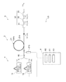
以下、本発明を実施するための形態について図面を参照しながら説明する。本発明の態様として例示するレーザ装置LSの概要構成図を図1に示す。レーザ装置LSは、パルス状のレーザ光(シード光)を発生するレーザ光発生部1と、レーザ光発生部1により発生されたシード光を増幅する増幅部2と、増幅部2から出力された増幅光を波長変換する波長変換部3と、これら各部の作動を制御する制御部8とを備えて構成される。
Hereinafter, embodiments for carrying out the present invention will be described with reference to the drawings. FIG. 1 shows a schematic configuration diagram of a laser apparatus LS exemplified as an aspect of the present invention. The laser device LS is output from the laser light generator 1 that generates pulsed laser light (seed light), the
レーザ光発生部1や増幅部2、波長変換部3の具体的な構成は、前述した特許文献等に開示されているように多数の構成形態がある。本実施形態においては、レーザ光発生部1において発生するシード光の波長を1.06μm帯の赤外光、波長変換部3から出力する出力光の波長を266nmの紫外光とした場合を例として説明する。
Specific configurations of the laser light generation unit 1, the
レーザ光発生部1は、波長帯域がともに1.06μm帯であるが、発振波長がわずかに異なる二つの光源を有して構成される。すなわち、レーザ光発生部1には、第1波長λ1のシード光を発生する第1光源11と、第2波長λ2のシード光を発生する第2光源12とが設けられる。ここでは、第1波長と第2波長との波長差Δλを8nmとし、第1波長λ1=1060nm、第2波長λ2=1068nmとする。
The laser light generator 1 has two light sources that have a wavelength band of 1.06 μm and have slightly different oscillation wavelengths. That is, the laser light generator 1 is provided with a
上記のような波長のシード光を発生する第1光源11及び第2光源12は、ともに発振波長が1.06μm帯のDFB(Distributed Feedback)半導体レーザを用いることができる。温度調整器により動作温度を制御することによって、DFB半導体レーザーの発振波長はある範囲の中で任意に設定することが可能である。DFB半導体レーザは、駆動電流を波形制御することによりCW発振及びパルス発振させることができる。本構成例においては、第1光源11及び第2光源12を1〜10MHz程度の所定の繰り返し周波数でパルス発振させる場合を主体として説明する。第1光源11及び第2光源12の作動は制御部8により制御される。レーザ光発生部1から出力されたパルス状の第1波長λ1のシード光Ls1及び第2波長λ2のシード光Ls2は、カプラ16により合波され増幅部2に入射する。
For both the
増幅部2は、レーザ光発生部1から出力されたシード光を増幅するファイバ増幅器21を備えて構成される。ファイバ増幅器21は、第1波長λ1及び第2波長λ2を含む波長1.06μm帯の光に利得を有するファイバ増幅器である。このようなファイバ増幅器として、イッテルビウム・ドープ・ファイバ増幅器(YDFA)を好適に用いることができる。
The
ファイバ増幅器(YDFA)21は、コアにイッテルビウム(Yb)がドープされた増幅用ファイバ21aと、増幅用ファイバに励起光を供給する励起光源21bとを主体として構成される。ファイバ増幅器21のゲインは、増幅用ファイバ21aを励起する励起光のパワーを制御すること、具体的には、制御部8が励起光源21bの駆動電力を制御することにより制御される。
The fiber amplifier (YDFA) 21 is mainly composed of an amplifying
YDFAは、波長が1000〜1100nmの帯域に利得を有するため、第1波長λ1=1060nmのシード光Ls1、及び第2波長λ2=1068nmのシード光Ls2を増幅することができる。また、カプラ16により合波されてファイバ増幅器21に入射する第1波長λ1のシード光Ls1及び第2波長λ2のシード光Ls2は、波長差Δλが8nm程度あるため各々独立して増幅され、第1波長のシード光Ls1が増幅された第1増幅光La1、及び第2波長のシード光Ls2が増幅された第2増幅光La2がファイバ増幅器21(増幅部2)から出力される。
Since YDFA has a gain in the band of wavelengths 1000 to 1100 nm, the seed light Ls 1 having the first wavelength λ 1 = 1060 nm and the seed light Ls 2 having the second wavelength λ 2 = 1068 nm can be amplified. Further, the seed light Ls 2 of the seed beam Ls 1 and the second wavelength lambda 2 of the first wavelength lambda 1 incident are combined by the
なお、説明簡明化のためファイバ増幅器21を単段で示したが、例えばシングルクラッドのファイバ増幅器を複数直列に接続し、あるいはシングルクラッドのファイバ増幅器とダブルクラッドのファイバ増幅器を直列に接続する等、複数のファイバ増幅器を直列に接続して増幅部2を構成することができる。増幅部2から出力された第1増幅光La1及び第2増幅光La2は、波長変換部3に入射する。
For simplicity, the
波長変換部3には、増幅部2から出力された第1増幅光La1及び第2増幅光La2が伝播する波長変換光学系30が設けられている。波長変換光学系30は、3つの波長変換光学素子31,32,33、すなわち第1波長変換光学素子31、第2波長変換素子32、第3波長変換光学素子33を主体とし、図示省略するレンズや波長板等を有して構成される。波長変換部3に入射した第1増幅光La1及び第2増幅光La2は、レンズを介して第1波長変換光学素子31に集光入射する。
The
第1波長変換光学素子31は、第2高調波発生(SHG:Second Harmonic Generation)により第1増幅光La1の第2高調波(第1変換光Lv1)を発生し、第2増幅光La2については波長変換することなく透過する非線形光学結晶である。このような第1波長変換光学素子31として、LBO(LiB3O5)結晶を用い、第1増幅光La1の第2高調波発生において位相整合条件を満たす所定温度(第1位相整合温度という)に調整設定して、非臨界位相整合(NCPM:Non Critical Phase Matching)で波長変換させる構成が例示される。
The first wavelength conversion
第1波長変換光学素子31で発生した波長530nmの第1変換光Lv1と、第1波長変換光学素子31を透過した波長1068nmの第2増幅光La2、並びに第1波長変換光学素子31を波長変換されずに透過した残余の第1増幅光La1は、第2波長変換光学素子32に入射する。
First converted light Lv 1 having a wavelength of 530 nm generated by the first wavelength converting
第2波長変換光学素子32は、第2高調波発生(SHG)により第2増幅光La2の第2高調波(第2変換光Lv2)を発生し、第1増幅光La1及び第1変換光Lv1については波長変換することなく透過する非線形光学結晶である。第2波長変換光学素子32として、第1波長変換光学素子31と同様のLBO結晶を用い、第2増幅光La2の第2高調波発生において位相整合条件を満たす第2位相整合温度に調整設定して、非臨界位相整合(NCPM)で波長変換させる構成が例示される。
The second wavelength conversion
位相整合が非臨界位相整合の場合には、発生する変換光(第1変換光Lv1及び第2変換光Lv2)にウォークオフが生じない。そのため、第1波長変換光学素子31及び第2波長変換素子32において各々十分な相互作用長を確保し、効率的に波長変換を行うことができる。また、出力される第1変換光Lv1及び第2変換光Lv2のビーム断面が楕円化するようなことがないため、ビーム断面を円形に整形するシリンドリカルレンズ等の整形光学素子を設ける必要がなく、第3波長変換光学素子33において効率的に波長変換することができる。
When the phase matching is non-critical phase matching, no walk-off occurs in the generated converted light (first converted light Lv 1 and second converted light Lv 2 ). Therefore, sufficient interaction length can be secured in each of the first wavelength conversion
上記のように、第1波長変換光学素子31は、第1増幅光La1を波長変換して第2高調波(第1変換光Lv1)を発生するが第2増幅光La2は波長変換することなく透過し、第2波長変換光学素子32は、第2増幅光La2を波長変換して第2高調波(第2変換光Lv2)を発生するが第1増幅光La1は波長変換することなく透過する。このような作用を実現する手段として、本技術においては、第1増幅光La1と第2増幅光La2との波長差Δλを利用する。換言すれば、第1波長変換光学素子31及び第2波長変換素子32において、いずれか一方の増幅光のみが位相整合条件を満たし、他方の増幅光は位相整合条件を満たさないように、第1波長λ1及び第2波長λ2が設定される。
As described above, the first wavelength conversion
第1,第2波長変換光学素子31,32としてLBO結晶を用いた場合について具体的に説明すると、例えば光軸方向の長さが20mm程度のLBO結晶を用いたときに、第1波長λ1または第2波長λ2について所定の位相整合温度で位相整合条件を満たす波長の許容幅(Δλ1,Δλ2)は数nm程度である。そのため、例えば第1波長変換光学素子31において、第1増幅光La1の第2高調波発生について位相整合条件を満たすように結晶温度を設定すれば、第1増幅光La1のみが位相整合条件を満たし、波長λが8nm異なる第2増幅光La2については位相整合条件を満たさない。第2波長変換光学素子32についても同様である。
The case where an LBO crystal is used as the first and second wavelength conversion
従って、第1波長変換光学素子31においては、第1増幅光La1のみが波長変換されて波長530nmの第1変換光Lv1が発生し、第2増幅光La2は波長変換されることなく第1波長変換光学素子31をそのまま透過する。また、第2波長変換光学素子32においては、第2増幅光La2のみが波長変換されて波長534nmの第2変換光Lv2が発生し、第1増幅光La1及び第1変換光Lv1は波長変換されることなく第2波長変換光学素子32をそのまま透過する。
Therefore, in the first wavelength conversion
以上では、第1波長変換光学素子31及び第2波長変換素子32としてLBO結晶を非臨界位相整合で用いた構成例について説明したが、本方法はLBO結晶やBBO(β-BaB2O4)結晶等の非線形光学結晶を臨界位相整合(CPM:Critical Phase Matching)で用いる構成についても、波長差Δλを利用して同様に適用することができる。例えば、第1増幅光La1について位相整合条件を満たすように第1波長変換光学素子31の角度位置を設定することによって、第1増幅光La1のみを波長変換して第1変換光Lv1を発生させ、第2増幅光La2は波長変換することなく透過させることができる。PPLN(Periodically Poled LiNbO3)結晶や、PPLT(Periodically Poled LiTaO3)結晶等の疑似位相整合(QPM:Quasi Phase Matching)結晶を用いる構成についても、波長差Δλを利用して同様に適用することができる。
In the above, the configuration example in which the LBO crystal is used in the non-critical phase matching as the first wavelength conversion
このようにして、第1波長変換光学素子31で発生し第2波長変換光学素子32を透過した波長530nmの第1変換光Lv1と、第2波長変換光学素子32で発生した波長534nmの第2変換光Lv2は、第3波長変換光学素子33に集光入射する。
Thus, the first converted light Lv 1 having a wavelength of 530 nm generated by the first wavelength conversion
第3波長変換光学素子33は、和周波発生(SFG:Sum Frequency Generation)により第1変換光Lv1と第2変換光Lv2との和周波を発生させる非線形光学結晶である。ここで、第3波長変換光学素子33に入射する光は、後述するように、第1変換光Lv1及び第2変換光Lv2が時間的に重複して入射する場合の他、第1変換光Lv1と第2変換光Lv2とが各々独立して入射する場合がある。しかし、第3波長変換光学素子33は、第1変換光Lv1と第2変換光Lv2との波長差Δλを利用して、第1変換光Lv1と第2変換光Lv2とは和周波発生の位相整合条件を満すが、第1変換光Lv1単体、及び第2変換光Lv2単体では和周波発生(第2高調波発生)の位相整合条件を満たさないように設定される。
The third wavelength conversion
第1変換光Lv1と第2変換光Lv2との和周波を発生させる第3波長変換光学素子33として、CLBO(CsLiB6O10)結晶を用い、第1変換光Lv1と第2変換光Lv2との和周波発生において位相整合条件を満たす所定の角度位置(位相整合角)に調整設定して、タイプIの臨界位相整合(CPM)で動作させる構成が例示される。第3波長変換光学素子33は、波長530nmの第1変換光Lv1と波長534nmの第2変換光Lv2との和周波発生によって波長266nmの第3変換光Lv3を発生させる位相整合条件に合わせて結晶が切り出される。
A CLBO (CsLiB 6 O 10 ) crystal is used as the third wavelength conversion
いま、第3波長変換光学素子33として、光軸方向の長さが10mm程度のCLBO結晶を用いた場合を想定すると、和周波発生の位相整合条件を満たす波長の許容幅(Δλ1,Δλ2)は〜0.2nm程度である。そのため、第1変換光Lv1と第2変換光Lv2とは位相整合条件を満たして波長266nmの第3変換光Lv3が発生するが、第1変換光Lv1単体、及び第2変換光Lv2単体では和周波発生の位相整合条件を満たさず、これらの第2高調波は発生しない。
Assuming that a CLBO crystal having a length in the optical axis direction of about 10 mm is used as the third wavelength conversion
第3波長変換光学素子33で発生した波長266nmの第3変換光Lv3は波長変換部3から出射され、レーザ装置LSから出力される。
The third converted light Lv 3 having a wavelength of 266 nm generated by the third wavelength conversion
以上、レーザ光発生部1、増幅部2、及び波長変換部3の構成について説明してきたが、レーザ装置LSにおいては、制御部8がレーザ光発生部1の作動を制御することにより、出力光である第3変換光Lv3を高速且つ安定的に制御可能になっている。既述したように、レーザ光発生部1には、第1波長λ1のシード光Ls1を発生する第1光源11と、第2波長λ2のシード光Ls2を発生する第2光源12とが設けられている。レーザ装置LSでは、制御部8が第1,第2光源の作動を制御することにより、出力光を高速且つ安定的に制御する。
The configuration of the laser light generation unit 1, the
制御部8には、各部の作動を制御する際に基準となる周波数100MHz程度のクロック信号を発生するクロック発生器80、クロック発生器80により発生されたクロック信号を基準として第1光源11を駆動する第1駆動信号及び第2光源12を駆動する第2駆動信号を生成する光源ドライバ81、レーザ装置LSが搭載されたシステムの加工プログラムや操作盤から入力される出力指令に基づいて光源ドライバ81に指令信号を出力する光源コントローラ83などを備えて構成される。
The
本構成例において、第1光源11を駆動する第1駆動信号、及び第2光源12を駆動する第2駆動信号は、ともにオン時間が1〜数nsecのパルスが、繰り返し周波数1〜10MHz程度で繰り返されるパルス列になっている。ここでは、第1駆動信号及び第2駆動信号を、ともにオン時間が1nsec、繰り返し周波数が1MHzのパルス列とする。
In this configuration example, the first drive signal for driving the
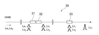
操作盤等から制御部8に入力される出力指令が、波長266nmの第3変換光(以下、「出力光」という)Lv3を出力するオン状態のとき、光源コントローラ83は、出力オン指令信号を光源ドライバ81に出力する。このとき、光源ドライバ81は、図2及び図3に示すように、第3波長変換光学素子33において第1変換光Lv1のパルス列と第2変換光Lv2のパルス列とが時間的に重なり合うように、第1光源11から出射する第1波長のシード光Ls1と第2光源12から出射する第2波長のシード光Ls2の相対的な出力タイミングを制御する。
When the output command input from the operation panel or the like to the
より具体的には、光源ドライバ81は第1変換光Lv1のパルス列と第2変換光Lv2のパルス列とが第3波長変換光学素子33において時間的に重なり合うタイミング(両者の光路長が同一の場合には同一タイミング)の第1駆動信号及び第2駆動信号を生成し、第1光源11及び第2光源12を駆動する。
More specifically, the
第1光源11から出射した第1波長のシード光Ls1、及び第2光源12から出射した第2波長のシード光Ls2は、各々ファイバ増幅器21により増幅されて第1増幅光La1及び第2増幅光La2となり、第1波長変換光学素子31に集光入射する。第1波長変換光学素子31においては、第1波長λ1と第2波長λ2との波長差Δλにより第1増幅光La1のみが波長変換されて第1変換光Lv1が発生し、第2増幅光La2は波長変換されずにそのまま透過する。第1波長変換光学素子31で発生した第1変換光Lv1、及び第1波長変換光学素子31をそのまま透過した第2増幅光La2は第2波長変換素子32に入射する。
The first wavelength seed light Ls 1 emitted from the
第2波長変換光学素子32においては、第1波長λ1と第2波長λ2との波長差Δλにより第2増幅光La2のみが波長変換されて第2変換光Lv2が発生する。第2波長変換光学素子32で発生した第2変換光Lv2と、波長変換光学素子32を透過した第1変換光Lv1は第3波長変換光学素子33に集光入射する。
In the second optical
第3波長変換光学素子33に入射する第1変換光Lv1と第2変換光Lv2とは、出力光を出射するオン状態のときに、第3波長変換光学素子33で両者のパルス列が時間的に重なり合うように設定されている。また既述したように、第3波長変換光学素子33は、第1変換光Lv1と第2変換光Lv2とが和周波発生の位相整合条件を満たし、第1変換光Lv1単体、及び第2変換光Lv2単体では第2高調波発生の位相整合条件を満たさないように設定されている。そのため、第3波長変換光学素子33において第1変換光Lv1と第2変換光Lv2との和周波発生により波長266nmの出力光(第3変換光)Lv3が発生し、レーザ装置LSから出力される。
When the first converted light Lv 1 and the second converted light Lv 2 incident on the third wavelength conversion
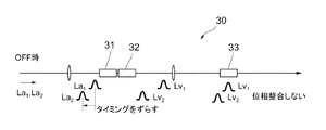
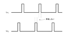
一方、操作盤等から制御部8に入力される出力指令が、出力光Lv3を停止するオフ状態のとき、光源コントローラ83は、出力オフ指令信号を光源ドライバ81に出力する。このとき、光源ドライバ81は、図4及び図5に示すように、第3波長変換光学素子33において第1変換光Lv1のパルス列と第2変換光Lv2のパルス列とが時間的に重なり合わないように、第1光源11から出射する第1波長のシード光Ls1と第2光源12から出射する第2波長のシード光Ls2の相対的な出力タイミングを制御する。
On the other hand, the
具体的には、光源ドライバ81は第1変換光Lv1のパルス列と第2変換光Lv2のパルス列とが第3波長変換光学素子33において時間的に重なり合わないタイミング(いずれか一方がオン状態のとき他方がオフ状態になるタイミング)の第1駆動信号及び第2駆動信号を生成し、第1光源11及び第2光源12を駆動する。
Specifically, the
第1光源11から出射した第1波長のシード光Ls1、及び第2光源12から出射した第2波長のシード光Ls2は、各々ファイバ増幅器21により増幅されて第1増幅光La1及び第2増幅光La2となり、第1波長変換光学素子31に集光入射する。第1波長変換光学素子31においては、第1波長λ1と第2波長λ2との波長差Δλにより第1増幅光La1のみが波長変換されて第1変換光Lv1が発生し、第2増幅光La2は波長変換されずにそのまま透過する。第1波長変換光学素子31で発生した第1変換光Lv1、及び第1波長変換光学素子31をそのまま透過した第2増幅光La2は第2波長変換素子32に入射する。
The first wavelength seed light Ls 1 emitted from the
第2波長変換光学素子32においては、第1波長λ1と第2波長λ2との波長差Δλにより第2増幅光La2のみが波長変換されて第2変換光Lv2が発生する。第2波長変換光学素子32で発生した第2変換光Lv2と、波長変換光学素子32を透過した第1変換光Lv1は第3波長変換光学素子33に集光入射する。
In the second optical
しかしこのときには、第3波長変換光学素子33に入射した第1変換光Lv1と第2変換光Lv2とは、第3波長変換光学素子33において両者のパルス列が時間的に重なり合わないように設定されている。また、第3波長変換光学素子33は、第1変換光Lv1と第2変換光Lv2とは和周波発生の位相整合条件を満たすが、第1変換光Lv1単体、及び第2変換光Lv2単体では第2高調波発生の位相整合条件を満たさないように設定されている。そのため、第3波長変換光学素子33において波長266nmの出力光Lv3は発生せず、レーザ装置LSから出力されない。
However, at this time, the first converted light Lv 1 and the second converted light Lv 2 incident on the third wavelength converting
以上のように第1光源11を駆動する第1駆動信号のパルス列と、第2光源12を駆動する第2駆動信号のパルス列との相対的なタイミングを変化させることによって、波長266nmの出力光Lv3をオン/オフが制御することができる。
As described above, by changing the relative timing of the pulse train of the first drive signal that drives the
なお、波長変換部3の出力端部に、例えば波長が300nm程度よりも短い光を反射し、波長がこれよりも長い光を透過するダイクロイックミラー等を設け、出力光Lv3と、第3波長変換光学素子33を透過した第1,第2増幅光及び第1,第2変換光等とを分離することによって、出力光以外の波長の光がレーザ装置LSから出力されることを防止することができる。
A dichroic mirror or the like that reflects light having a wavelength shorter than about 300 nm and transmits light having a wavelength longer than this is provided at the output end of the
以上では、レーザ装置LSから出力する出力光Lv3をオン/オフ制御する形態について説明したが、本構成のレーザ装置LSは、出力光Lv3のパワーを制御することもできる。上述したように、出力光Lv3をオン/オフする制御は、第1変換光Lv1のパルス列と第2変換光Lv2のパルス列とが第3波長変換光学素子33において時間的に重なり合う状態と、時間的に重なり合わない状態とに切り換えることによって実現される(図2〜図5を参照)。一方、出力光Lv3のパワーを変化させる制御は、第1変換光Lv1のパルス列と第2変換光Lv2のパルス列とが、第3波長変換光学素子33において時間的に重なる重複率を制御することによって実現される。この出力光のパワー制御も、具体的には、第1光源11を駆動する第1駆動信号と、第2光源を駆動する第2駆動信号との相対的なタイミングを変化させることにより行われる。
In the above description, the on / off control of the output light Lv 3 output from the laser device LS has been described. However, the laser device LS having this configuration can also control the power of the output light Lv 3 . As described above, the control for turning on / off the output light Lv 3 is performed in a state where the pulse train of the first converted light Lv 1 and the pulse train of the second converted light Lv 2 overlap in time in the third wavelength conversion
図6(a)〜(c)は、第1駆動信号と第2駆動信号との相対的なタイミングを変化させることにより、第3波長変換光学素子33における第1変換光Lv1のパルス列と第2変換光Lv2のパルス列との重複率を変化させた様子を示す説明図である。この図における(a)は、第3波長変換光学素子33における第1変換光Lv1のパルス列と第2変換光Lv2のパルス列との重複率を20%に設定した場合、(b)は両者の重複率を約50%に設定した場合、(c)は両者の重複率を80%に設定した場合を例示する。
6A to 6C show the pulse train of the first converted light Lv 1 in the third wavelength conversion
図6(a)に示す重複率20%の場合には、第3波長変換光学素子33で発生する出力光Lv3のパワーは、重複率が100%のときのパワーの20%になる。同様に図6(b)に示す重複率50%の場合には出力光Lv3のパワーは重複率100%のときのパワーの50%、図6(c)に示す重複率80%の場合には出力光Lv3のパワーは重複率100%のときのパワーの80%になる。
In the case of the overlap rate of 20% shown in FIG. 6A, the power of the output light Lv 3 generated by the third wavelength conversion
すなわち、第1光源11を駆動する第1駆動信号と第2光源12を駆動する第2駆動信号との相対的なタイミングを変化させて、第3波長変換光学素子33における第1変換光Lv1のパルス列と第2変換光Lv2のパルス列との重複率を変化させることにより、0〜100%の範囲で出力光Lv3のパワーを任意かつ高速に制御することができる。
That is, the first converted light Lv 1 in the third wavelength conversion
このような構成のレーザ装置LSにおいては、レーザ光発生部1において、出力光Lv3をオン/オフするために第1光源11及び第2光源12の少なくともいずれかを動作状態と非動作状態とに切り替えたり、出力光Lv3のパワーを制御するために第1光源11を駆動する第1駆動信号及び第2光源12を駆動する第2駆動信号の少なくともいずれかの信号波形を変化させたりする必要がなく、第1光源11及び第2光源12の両者をともに定常状態で動作させることができる。このため、第1光源11及び第2光源12を安定的に動作させ、発振波長及びパルス波形が安定した第1波長のシード光Ls1及び第2波長のシード光Ls2を発生させることができる。
In the laser apparatus LS having such a configuration, at least one of the
また、増幅部2では、ファイバ増幅器21に第1光源11で発生した第1波長のシード光Ls1及び第2光源で発生した第2波長のシード光Ls2が常時入射し、ファイバ増幅器21において各々増幅されて第1増幅光La1及び第2増幅光La2が定常的に出力される。このため、出力光Lv3をオン/オフしたり出力光Lv3のパワーを制御するためにファイバ増幅器21のゲインを変化させる必要がなく、ファイバ増幅器21を定常状態で安定的に動作させて第1増幅光La1及び第2増幅光La2を安定的に出力させることができる。
In the
さらに、波長変換部3においては、第1波長変換光学素子31に第1増幅光La1及び第2増幅光La2が常時入射して第1変換光Lv1が定常的に発生し、第2波長変換光学素子32には第1変換光Lv1及び第2増幅光La2が常時入射して第2変換光Lv2が定常的に発生する。また、第3波長変換光学素子33には第1波長変換光学素子31で発生した第1変換光Lv1と第1波長変換光学素子31で発生したと第2変換光Lv2とが常時入射する。そのため、第3波長変換光学素子33における出力光Lv3のパワーに応じた発熱量変化を除いて、第1〜第3波長変換光学素子31〜33は熱的に安定であり、特に第2波長変換光学素子32までの熱的な状態は極めて安定している。
Furthermore, in the
従って、このようなレーザ装置LSによれば、増幅部2のファイバ増幅器21と波長変換部3の第1〜第3波長変換光学素子31〜33を直列的に接続し、レーザ光発生部1の第1光源11を駆動する第1駆動信号と第2光源12を駆動する第2駆動信号との相対的なタイミングを変化させる簡明な構成で、出力光Lv3を高速且つ安定的に制御することができる。
Therefore, according to such a laser device LS, the
以上では、第1光源11及び第2光源12をパルス発振させ、その駆動信号の相対的なタイミングを変化させることによって出力光(第3変換光)の出力状態を制御する構成を例示した。しかし、本発明は上記構成形態に限らず、レーザ光発生部1から出力される第1波長のシード光Ls1と第2波長のシード光Ls2の出力タイミングを高速に制御可能な構成であればよい。
In the above, the configuration in which the output state of the output light (third converted light) is controlled by pulsating the
例えば、第1光源11及び第2光源12の少なくともいずれかの出射端部に電気光学変調器(EOM)等の外部変調器を設け、CW発振またはパルス発振させたレーザ光の一部を外部変調器により前記所定のタイミングで切り出して、第1波長のシード光Ls1及び第2波長のシード光Ls2をレーザ光発生部1から出力するように構成しても良い。このような形態のレーザ装置においても、前述したレーザ装置LSと同様の作用及び効果を得ることができ、さらにパルス波形の立ち上がり及び立ち下がりが、より急峻な出力光を出力することができる。
For example, an external modulator such as an electro-optic modulator (EOM) is provided at the emission end of at least one of the
なお、実施形態では、第1波長λ1と第2波長λ2との波長差Δλを8nmとした構成を例示したが、波長差Δλは増幅部2や波長変換部3の構成に応じて、適宜な値に設定することができる。すなわち、波長差Δλは、1本のファイバ増幅器21において第1波長λ1のシード光及び第2波長λ2のシード光を並立して増幅可能であり、また第3波長変換光学素子33において第1変換光Lv1と第2変換光Lv2のみが位相整合条件を満たすような波長差であればよい。なお、第1波長変換光学素子31において第1増幅光La1のみが位相整合条件を満たし、第2波長変換光学素子32において第2増幅光L2のみが位相整合条件を満たす他の構成として、第1増幅光La1と第2増幅光La2の偏光面の角度を直交させて第1波長変換光学素子31に入射する手法が例示される。この場合、第1波長変換光学素子31と第2波長変換光学素子32の間に、第2増幅光La2の偏光方向を90度回転させる一方第1変換光Lv1の偏光方向を保持するような2波長波長板を挿入するか、第3波長変換光学素子33をタイプIIの位相整合条件(2つの基本波の偏光方向が直交)で用いれば良い。
In the embodiment, the configuration in which the wavelength difference Δλ between the first wavelength λ 1 and the second wavelength λ 2 is 8 nm is illustrated, but the wavelength difference Δλ depends on the configuration of the
また、実施形態では、レーザ光発生部1から波長1.06μm帯のシード光を出力し、波長変換部3の三つの波長変換光学素子31,32,33で波長266nmの出力光に波長変換して出力する構成を例示したが、シード光の波長帯域や波長変換光学素子の個数及び配置、出力光の波長等は任意である。
In the embodiment, seed light having a wavelength of 1.06 μm is output from the laser light generation unit 1 and converted into output light having a wavelength of 266 nm by the three wavelength conversion
以上説明したようなレーザ装置LSは、小型軽量であるとともに取り扱いが容易であり、露光装置や光造形装置等の光加工装置、フォトマスクやウェハ等の検査装置、顕微鏡や望遠鏡等の観察装置、測長器や形状測定器等の測定装置、光治療装置などのシステムに好適に適用することができる。 The laser device LS as described above is small and light and easy to handle, optical processing devices such as exposure devices and stereolithography devices, inspection devices such as photomasks and wafers, observation devices such as microscopes and telescopes, The present invention can be suitably applied to a measuring device such as a length measuring device or a shape measuring device, and a system such as a phototherapy device.
レーザ装置LSを備えたシステムの第1の適用例として、半導体製造や液晶パネル製造のフォトリソグラフィ工程で用いられる露光装置について、その概要構成を示す図7を参照して説明する。露光装置500は、原理的には写真製版と同じであり、石英ガラス製のフォトマスク513に精密に描かれたデバイスパターンを、フォトレジストを塗布した半導体ウェハやガラス基板などの露光対象物515に光学的に投影して転写する。
As a first application example of a system including the laser device LS, an exposure apparatus used in a photolithography process for manufacturing a semiconductor or a liquid crystal panel will be described with reference to FIG. The
露光装置500は、上述したレーザ装置LSと、照明光学系502と、フォトマスク513を保持するマスク支持台503と、投影光学系504と、露光対象物515を保持する露光対象物支持テーブル505と、露光対象物支持テーブル505を水平面内で移動させる駆動機構506とを備えて構成される。照明光学系502は複数のレンズ群からなり、レーザ装置LSから出力されたレーザ光を、マスク支持台503に保持されたフォトマスク513に照射する。投影光学系504も複数のレンズ群により構成され、フォトマスク513を透過した光を露光対象物支持テーブル上の露光対象物515に投影する。
The
このような構成の露光装置500においては、レーザ装置LSから出力されたレーザ光が照明光学系502に入力され、所定光束に調整されたレーザ光がマスク支持台503に保持されたフォトマスク513に照射される。フォトマスク513を通過した光はフォトマスク513に描かれたデバイスパターンの像を有しており、この光が投影光学系504を介して露光対象物支持テーブル505に保持された露光対象物515の所定位置に照射される。これにより、フォトマスク513のデバイスパターンの像が、半導体ウェハや液晶パネル等の露光対象物515の上に所定倍率で結像露光される。
In the
次に、レーザ装置LSを備えたシステムの第2の適用例として、フォトマスクや液晶パネル、ウェハ等(被検物)の検査工程で使用される検査装置について、その概要構成を示す図8を参照して説明する。図8に例示する検査装置600は、フォトマスク等の光透過性を有する被検物613に描かれた微細なデバイスパターンの検査に好適に使用される。
Next, as a second application example of the system including the laser device LS, FIG. 8 showing a schematic configuration of an inspection device used in an inspection process of a photomask, a liquid crystal panel, a wafer, or the like (test object). The description will be given with reference. An
検査装置600は、前述したレーザ装置LSと、照明光学系602と、被検物613を保持する被検物支持台603と、投影光学系604と、被検物613からの光を検出するTDI(Time Delay Integration)センサ615と、被検物支持台603を水平面内で移動させる駆動機構606とを備えて構成される。照明光学系602は複数のレンズ群からなり、レーザ装置LSから出力されたレーザ光を、所定光束に調整して被検物支持台603に保持された被検物613に照射する。投影光学系604も複数のレンズ群により構成され、被検物613を透過した光をTDIセンサ615に投影する。
The
このような構成の検査装置600においては、レーザ装置LSから出力されたレーザ光が照明光学系602に入力され、所定光束に調整されたレーザ光が被検物支持台603に保持されたフォトマスク等の被検物613に照射される。被検物613からの光(本構成例においては透過光)は、被検物613に描かれたデバイスパターンの像を有しており、この光が投影光学系604を介してTDIセンサ615に投影され結像する。このとき、駆動機構606による被検物支持台603の水平移動速度と、TDIセンサ615の転送クロックとは同期して制御される。
In the
そのため、被検物613のデバイスパターンの像がTDIセンサ615により検出され、このようにして検出された被検物613の検出画像と、予め設定された所定の参照画像とを比較することにより、被検物に描かれた微細パターンの欠陥が抽出される。なお、被検物613がウェハ等のように光透過性を有さない場合には、被検物からの反射光を投影光学系604に入射してTDIセンサ615に導くことにより、同様に構成することができる。
Therefore, an image of the device pattern of the
LS レーザ装置
1 レーザ光発生部 2 増幅部
3 波長変換部 8 制御部
11 第1光源 12 第2光源
21 ファイバ増幅器(増幅器) 30 波長変換光学系
31 第1波長変換光学素子 32 第2波長変換光学素子
33 第3波長変換光学素子
Ls1 第1波長のシード光 Ls2 第2波長のシード光
La1 第1増幅光 La2 第2増幅光
Lv1 第1変換光 Lv2 第2変換光
Lv3 第3変換光(出力光)
500 露光装置
502 照明光学系 503 マスク支持台
504 投影光学系 505 露光対象物支持テーブル
513 フォトマスク 515 露光対象物
600 検査装置
602 照明光学系 603 被検物支持台
604 投影光学系 613 被検物
615 TDIセンサ
LS laser apparatus 1 Laser
DESCRIPTION OF
Claims (7)
前記第1波長及び前記第2波長を含む波長帯域の光に利得を有する増幅器を備え、前記レーザ光発生部から出力された前記第1波長のレーザ光及び前記第2波長のレーザ光を増幅して、前記第1波長のレーザ光を増幅した第1増幅光及び前記第2波長のレーザ光を増幅した第2増幅光を出力する増幅部と、
前記増幅部から出力された前記第1増幅光を第1変換光に波長変換し前記第2増幅光を透過する第1波長変換光学素子、前記第1波長変換光学素子を透過した前記第2増幅光を第2変換光に波長変換し前記第1変換光を透過する第2波長変換光学素子、及び前記第1変換光と前記第2変換光とから波長変換により第3変換光を発生する第3波長変換光学素子を有する波長変換部と、
前記レーザ光発生部の作動を制御する制御部とを備え、
前記制御部が、前記レーザ光発生部から出力するパルス状の前記第1波長のレーザ光及びパルス状の前記第2波長のレーザ光の相対的な出力タイミングを制御することにより、前記第3波長変換光学素子における前記第1変換光と前記第2変換光との時間的な重ね合わせを制御して、前記第3変換光の出力状態を制御する
ように構成したことを特徴とするレーザ装置。 A laser light generator having a first light source for generating a pulsed first wavelength laser beam and a second light source for generating a pulsed second wavelength laser beam;
An amplifier having a gain for light in a wavelength band including the first wavelength and the second wavelength, and amplifying the laser light of the first wavelength and the laser light of the second wavelength output from the laser light generation unit. An amplifying unit that outputs a first amplified light obtained by amplifying the laser light having the first wavelength and a second amplified light obtained by amplifying the laser light having the second wavelength;
The first wavelength conversion optical element that converts the wavelength of the first amplified light output from the amplification section into first converted light and transmits the second amplified light, and the second amplification that transmits the first wavelength converted optical element A second wavelength-converting optical element that converts the wavelength of light into second converted light and transmits the first converted light; and a third wavelength-converted optical element that generates third converted light from the first converted light and the second converted light. A wavelength converter having a three-wavelength conversion optical element;
A control unit for controlling the operation of the laser light generation unit,
The control unit controls the relative output timings of the pulsed first wavelength laser beam and the pulsed second wavelength laser beam output from the laser beam generation unit, whereby the third wavelength A laser apparatus configured to control temporal superposition of the first converted light and the second converted light in a conversion optical element to control an output state of the third converted light.
前記第3波長変換光学素子において、前記第1変換光と前記第2変換光とは位相整合条件を満たすが、前記第1変換光単体及び前記第2変換光単体では位相整合条件を満たさないような波長に設定される
ことを特徴とする請求項1に記載のレーザ装置。 The first wavelength and the second wavelength are:
In the third wavelength conversion optical element, the first converted light and the second converted light satisfy a phase matching condition, but the first converted light alone and the second converted light do not satisfy the phase matching condition. The laser device according to claim 1, wherein the laser device is set to a different wavelength.
前記第1波長変換光学素子において、前記第1増幅光は位相整合条件を満たすが前記第2増幅光は位相整合条件を満たさず、
前記第2波長変換光学素子において、前記第2増幅光は位相整合条件を満たすが前記第1増幅光は位相整合条件を満たさないような波長に設定される
ことを特徴とする請求項1または2に記載のレーザ装置。 The first wavelength and the second wavelength are:
In the first wavelength conversion optical element, the first amplified light satisfies a phase matching condition, but the second amplified light does not satisfy a phase matching condition.
3. The second wavelength conversion optical element according to claim 1, wherein the second amplified light is set to a wavelength that satisfies a phase matching condition, but the first amplified light does not satisfy a phase matching condition. The laser device described in 1.
ことを特徴とする請求項1〜3のいずれか一項に記載のレーザ装置。 The control unit switches on / off the third converted light by switching between the state in which the first converted light and the second converted light overlap with each other in the third wavelength conversion optical element. The laser device according to any one of claims 1 to 3, wherein OFF is controlled.
ことを特徴とする請求項1〜4のいずれか一項に記載のレーザ装置。 The control unit controls the power of the third converted light by changing a temporal overlap rate between the first converted light and the second converted light in the third wavelength conversion optical element. The laser device according to any one of claims 1 to 4.
所定の露光パターンが形成されたフォトマスクを保持するマスク支持部と、
露光対象物を保持する露光対象物支持部と、
前記レーザ装置から出力されたレーザ光を前記マスク支持部に保持されたフォトマスクに照射する照明光学系と、
前記フォトマスクを透過した光を露光対象物支持部に保持された露光対象物に投影する投影光学系と
を備えたことを特徴とする露光装置。 A laser device according to any one of claims 1 to 5;
A mask support for holding a photomask on which a predetermined exposure pattern is formed;
An exposure object support for holding the exposure object;
An illumination optical system for irradiating the photomask held by the mask support with the laser beam output from the laser device;
An exposure apparatus comprising: a projection optical system that projects light transmitted through the photomask onto an exposure target held by an exposure target support.
被検物を保持する被検物支持部と、
前記レーザ装置から出力されたレーザ光を前記被検物支持部に保持された被検物に照射する照明光学系と、
前記被検物からの光を検出器に投影する投影光学系と
を備えたことを特徴とする検査装置。 A laser device according to any one of claims 1 to 5;
An object support for holding the object;
An illumination optical system for irradiating a test object held by the test object support unit with laser light output from the laser device;
An inspection apparatus comprising: a projection optical system that projects light from the test object onto a detector.
Priority Applications (6)
| Application Number | Priority Date | Filing Date | Title |
|---|---|---|---|
| JP2012169643A JP2015180902A (en) | 2012-07-31 | 2012-07-31 | LASER DEVICE, EXPOSURE DEVICE AND INSPECTION DEVICE EQUIPPED WITH THIS LASER DEVICE |
| KR1020207007282A KR20200030633A (en) | 2012-07-31 | 2013-07-31 | Laser device, and exposure device and inspection device equipped with said laser device |
| PCT/JP2013/070717 WO2014021370A1 (en) | 2012-07-31 | 2013-07-31 | Laser device, and exposure device and inspection device equipped with said laser device |
| US14/417,986 US9608400B2 (en) | 2012-07-31 | 2013-07-31 | Laser device, and exposure device and inspection device provided with laser device |
| KR1020157005321A KR102090454B1 (en) | 2012-07-31 | 2013-07-31 | Laser device, and exposure device and inspection device equipped with said laser device |
| CN201380050529.8A CN104685414B (en) | 2012-07-31 | 2013-07-31 | Laser device, exposure device including same, and inspection device |
Applications Claiming Priority (1)
| Application Number | Priority Date | Filing Date | Title |
|---|---|---|---|
| JP2012169643A JP2015180902A (en) | 2012-07-31 | 2012-07-31 | LASER DEVICE, EXPOSURE DEVICE AND INSPECTION DEVICE EQUIPPED WITH THIS LASER DEVICE |
Publications (1)
| Publication Number | Publication Date |
|---|---|
| JP2015180902A true JP2015180902A (en) | 2015-10-15 |
Family
ID=54329186
Family Applications (1)
| Application Number | Title | Priority Date | Filing Date |
|---|---|---|---|
| JP2012169643A Pending JP2015180902A (en) | 2012-07-31 | 2012-07-31 | LASER DEVICE, EXPOSURE DEVICE AND INSPECTION DEVICE EQUIPPED WITH THIS LASER DEVICE |
Country Status (1)
| Country | Link |
|---|---|
| JP (1) | JP2015180902A (en) |
Cited By (1)
| Publication number | Priority date | Publication date | Assignee | Title |
|---|---|---|---|---|
| CN109154727A (en) * | 2016-05-26 | 2019-01-04 | 株式会社尼康 | Pulsed light generating means, pulsed light generation method, the exposure device and check device for having pulsed light generating means |
-
2012
- 2012-07-31 JP JP2012169643A patent/JP2015180902A/en active Pending
Cited By (7)
| Publication number | Priority date | Publication date | Assignee | Title |
|---|---|---|---|---|
| CN109154727A (en) * | 2016-05-26 | 2019-01-04 | 株式会社尼康 | Pulsed light generating means, pulsed light generation method, the exposure device and check device for having pulsed light generating means |
| KR20190011738A (en) * | 2016-05-26 | 2019-02-07 | 가부시키가이샤 니콘 | Pulsed light generating apparatus, pulse light generating method, exposure apparatus having pulse light generating apparatus, and inspection apparatus |
| JPWO2017204113A1 (en) * | 2016-05-26 | 2019-04-25 | 株式会社ニコン | Pulse light generation apparatus, pulse light generation method, exposure apparatus and inspection apparatus provided with pulse light generation apparatus |
| TWI733814B (en) * | 2016-05-26 | 2021-07-21 | 日商尼康股份有限公司 | Pulsed light generating device, pulsed light generating method, exposure device and inspection device provided with pulsed light generating device |
| KR102358736B1 (en) | 2016-05-26 | 2022-02-04 | 가부시키가이샤 니콘 | Pulsed light generating apparatus, pulsed light generating method, exposure apparatus and inspection apparatus provided with pulsed light generating apparatus |
| CN109154727B (en) * | 2016-05-26 | 2022-02-22 | 株式会社尼康 | Pulse light generating apparatus, pulse light generating method, exposure apparatus and inspection apparatus provided with pulse light generating apparatus |
| US11366070B2 (en) | 2016-05-26 | 2022-06-21 | Nikon Corporation | Pulsed light generation device, pulsed light generation method, exposure apparatus having pulsed light generation device and inspection apparatus having pulsed light generation device |
Similar Documents
| Publication | Publication Date | Title |
|---|---|---|
| JP6311720B2 (en) | LASER DEVICE, EXPOSURE DEVICE AND INSPECTION DEVICE EQUIPPED WITH THE LASER DEVICE | |
| CN104685414B (en) | Laser device, exposure device including same, and inspection device | |
| JP6016086B2 (en) | Ultraviolet laser apparatus, exposure apparatus and inspection apparatus equipped with the ultraviolet laser apparatus | |
| JP6304365B2 (en) | Pulse light generation method, pulse laser apparatus, exposure apparatus and inspection apparatus including the pulse laser apparatus, and electronic device manufacturing method | |
| US9429850B2 (en) | Laser device, and exposure device and inspection device provided with laser device | |
| JP6016124B2 (en) | Pulse laser apparatus, exposure apparatus and inspection apparatus | |
| JP2013156448A (en) | Laser device, exposure device and inspection device | |
| JP2010003771A (en) | Seed light generating device, light source device and method for adjusting the same, optical irradiation apparatus, exposure apparatus, and device manufacturing method | |
| JP5359461B2 (en) | Laser apparatus, light source apparatus, adjustment method thereof, light irradiation apparatus, exposure apparatus, and device manufacturing method | |
| JP2014036152A (en) | Fiber laser, laser device including fiber laser, exposure device and inspection device | |
| JP2015180903A (en) | LASER DEVICE, EXPOSURE DEVICE AND INSPECTION DEVICE EQUIPPED WITH THE LASER DEVICE | |
| KR102393457B1 (en) | Pulsed light generating apparatus, pulsed light generating method, exposure apparatus and inspection apparatus provided with pulsed light generating apparatus | |
| CN103348286A (en) | Ultraviolet laser device | |
| JP2015180902A (en) | LASER DEVICE, EXPOSURE DEVICE AND INSPECTION DEVICE EQUIPPED WITH THIS LASER DEVICE | |
| JP6299589B2 (en) | Ultraviolet laser apparatus, exposure apparatus and inspection apparatus equipped with the ultraviolet laser apparatus | |
| JP2013044764A (en) | Laser device, method for suppressing photorefractive effect of quasi-phase-matching wavelength conversion optical element, exposure device, and inspection device | |
| JP2013007931A (en) | Laser device, exposure device and inspecting device | |
| JP2012252289A (en) | Laser device, exposure apparatus, and inspection apparatus | |
| JP2013004597A (en) | Laser device, exposure apparatus with laser device and inspection apparatus | |
| JP5780457B2 (en) | Laser apparatus, exposure apparatus equipped with laser apparatus, and inspection apparatus | |
| JP2011069945A (en) | Method for generating laser beam | |
| JP5397773B2 (en) | Light source device | |
| JP2010237234A (en) | Light source device and adjustment method thereof |