JP2015201250A - semiconductor device - Google Patents
semiconductor device Download PDFInfo
- Publication number
- JP2015201250A JP2015201250A JP2015120001A JP2015120001A JP2015201250A JP 2015201250 A JP2015201250 A JP 2015201250A JP 2015120001 A JP2015120001 A JP 2015120001A JP 2015120001 A JP2015120001 A JP 2015120001A JP 2015201250 A JP2015201250 A JP 2015201250A
- Authority
- JP
- Japan
- Prior art keywords
- transistor
- potential
- electrode
- insulating layer
- circuit
- Prior art date
- Legal status (The legal status is an assumption and is not a legal conclusion. Google has not performed a legal analysis and makes no representation as to the accuracy of the status listed.)
- Withdrawn
Links
Images


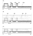


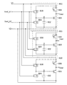


Classifications
-
- G—PHYSICS
- G11—INFORMATION STORAGE
- G11C—STATIC STORES
- G11C11/00—Digital stores characterised by the use of particular electric or magnetic storage elements; Storage elements therefor
- G11C11/21—Digital stores characterised by the use of particular electric or magnetic storage elements; Storage elements therefor using electric elements
- G11C11/34—Digital stores characterised by the use of particular electric or magnetic storage elements; Storage elements therefor using electric elements using semiconductor devices
- G11C11/40—Digital stores characterised by the use of particular electric or magnetic storage elements; Storage elements therefor using electric elements using semiconductor devices using transistors
- G11C11/401—Digital stores characterised by the use of particular electric or magnetic storage elements; Storage elements therefor using electric elements using semiconductor devices using transistors forming cells needing refreshing or charge regeneration, i.e. dynamic cells
- G11C11/4063—Auxiliary circuits, e.g. for addressing, decoding, driving, writing, sensing or timing
- G11C11/407—Auxiliary circuits, e.g. for addressing, decoding, driving, writing, sensing or timing for memory cells of the field-effect type
- G11C11/409—Read-write [R-W] circuits
- G11C11/4093—Input/output [I/O] data interface arrangements, e.g. data buffers
-
- G—PHYSICS
- G11—INFORMATION STORAGE
- G11C—STATIC STORES
- G11C11/00—Digital stores characterised by the use of particular electric or magnetic storage elements; Storage elements therefor
- G11C11/21—Digital stores characterised by the use of particular electric or magnetic storage elements; Storage elements therefor using electric elements
- G11C11/34—Digital stores characterised by the use of particular electric or magnetic storage elements; Storage elements therefor using electric elements using semiconductor devices
- G11C11/40—Digital stores characterised by the use of particular electric or magnetic storage elements; Storage elements therefor using electric elements using semiconductor devices using transistors
- G11C11/401—Digital stores characterised by the use of particular electric or magnetic storage elements; Storage elements therefor using electric elements using semiconductor devices using transistors forming cells needing refreshing or charge regeneration, i.e. dynamic cells
- G11C11/403—Digital stores characterised by the use of particular electric or magnetic storage elements; Storage elements therefor using electric elements using semiconductor devices using transistors forming cells needing refreshing or charge regeneration, i.e. dynamic cells with charge regeneration common to a multiplicity of memory cells, i.e. external refresh
- G11C11/405—Digital stores characterised by the use of particular electric or magnetic storage elements; Storage elements therefor using electric elements using semiconductor devices using transistors forming cells needing refreshing or charge regeneration, i.e. dynamic cells with charge regeneration common to a multiplicity of memory cells, i.e. external refresh with three charge-transfer gates, e.g. MOS transistors, per cell
-
- G—PHYSICS
- G11—INFORMATION STORAGE
- G11C—STATIC STORES
- G11C11/00—Digital stores characterised by the use of particular electric or magnetic storage elements; Storage elements therefor
- G11C11/21—Digital stores characterised by the use of particular electric or magnetic storage elements; Storage elements therefor using electric elements
- G11C11/34—Digital stores characterised by the use of particular electric or magnetic storage elements; Storage elements therefor using electric elements using semiconductor devices
- G11C11/40—Digital stores characterised by the use of particular electric or magnetic storage elements; Storage elements therefor using electric elements using semiconductor devices using transistors
- G11C11/401—Digital stores characterised by the use of particular electric or magnetic storage elements; Storage elements therefor using electric elements using semiconductor devices using transistors forming cells needing refreshing or charge regeneration, i.e. dynamic cells
- G11C11/4063—Auxiliary circuits, e.g. for addressing, decoding, driving, writing, sensing or timing
- G11C11/407—Auxiliary circuits, e.g. for addressing, decoding, driving, writing, sensing or timing for memory cells of the field-effect type
- G11C11/4074—Power supply or voltage generation circuits, e.g. bias voltage generators, substrate voltage generators, back-up power, power control circuits
-
- G—PHYSICS
- G11—INFORMATION STORAGE
- G11C—STATIC STORES
- G11C11/00—Digital stores characterised by the use of particular electric or magnetic storage elements; Storage elements therefor
- G11C11/21—Digital stores characterised by the use of particular electric or magnetic storage elements; Storage elements therefor using electric elements
- G11C11/34—Digital stores characterised by the use of particular electric or magnetic storage elements; Storage elements therefor using electric elements using semiconductor devices
- G11C11/40—Digital stores characterised by the use of particular electric or magnetic storage elements; Storage elements therefor using electric elements using semiconductor devices using transistors
- G11C11/401—Digital stores characterised by the use of particular electric or magnetic storage elements; Storage elements therefor using electric elements using semiconductor devices using transistors forming cells needing refreshing or charge regeneration, i.e. dynamic cells
- G11C11/4063—Auxiliary circuits, e.g. for addressing, decoding, driving, writing, sensing or timing
- G11C11/407—Auxiliary circuits, e.g. for addressing, decoding, driving, writing, sensing or timing for memory cells of the field-effect type
- G11C11/408—Address circuits
- G11C11/4085—Word line control circuits, e.g. word line drivers, - boosters, - pull-up, - pull-down, - precharge
-
- G—PHYSICS
- G11—INFORMATION STORAGE
- G11C—STATIC STORES
- G11C11/00—Digital stores characterised by the use of particular electric or magnetic storage elements; Storage elements therefor
- G11C11/21—Digital stores characterised by the use of particular electric or magnetic storage elements; Storage elements therefor using electric elements
- G11C11/34—Digital stores characterised by the use of particular electric or magnetic storage elements; Storage elements therefor using electric elements using semiconductor devices
- G11C11/40—Digital stores characterised by the use of particular electric or magnetic storage elements; Storage elements therefor using electric elements using semiconductor devices using transistors
- G11C11/401—Digital stores characterised by the use of particular electric or magnetic storage elements; Storage elements therefor using electric elements using semiconductor devices using transistors forming cells needing refreshing or charge regeneration, i.e. dynamic cells
- G11C11/4063—Auxiliary circuits, e.g. for addressing, decoding, driving, writing, sensing or timing
- G11C11/407—Auxiliary circuits, e.g. for addressing, decoding, driving, writing, sensing or timing for memory cells of the field-effect type
- G11C11/409—Read-write [R-W] circuits
- G11C11/4096—Input/output [I/O] data management or control circuits, e.g. reading or writing circuits, I/O drivers or bit-line switches
-
- H—ELECTRICITY
- H10—SEMICONDUCTOR DEVICES; ELECTRIC SOLID-STATE DEVICES NOT OTHERWISE PROVIDED FOR
- H10B—ELECTRONIC MEMORY DEVICES
- H10B41/00—Electrically erasable-and-programmable ROM [EEPROM] devices comprising floating gates
- H10B41/70—Electrically erasable-and-programmable ROM [EEPROM] devices comprising floating gates the floating gate being an electrode shared by two or more components
-
- H—ELECTRICITY
- H10—SEMICONDUCTOR DEVICES; ELECTRIC SOLID-STATE DEVICES NOT OTHERWISE PROVIDED FOR
- H10D—INORGANIC ELECTRIC SEMICONDUCTOR DEVICES
- H10D86/00—Integrated devices formed in or on insulating or conducting substrates, e.g. formed in silicon-on-insulator [SOI] substrates or on stainless steel or glass substrates
- H10D86/201—Integrated devices formed in or on insulating or conducting substrates, e.g. formed in silicon-on-insulator [SOI] substrates or on stainless steel or glass substrates the substrates comprising an insulating layer on a semiconductor body, e.g. SOI
Landscapes
- Engineering & Computer Science (AREA)
- Microelectronics & Electronic Packaging (AREA)
- Computer Hardware Design (AREA)
- Databases & Information Systems (AREA)
- Semiconductor Memories (AREA)
- Thin Film Transistor (AREA)
- Dram (AREA)
- Non-Volatile Memory (AREA)
- Metal-Oxide And Bipolar Metal-Oxide Semiconductor Integrated Circuits (AREA)
- Physical Vapour Deposition (AREA)
- Electrodes Of Semiconductors (AREA)
Abstract
Description
開示する発明は、半導体素子を利用した半導体装置およびその駆動方法に関するものであ
る。
The disclosed invention relates to a semiconductor device using a semiconductor element and a driving method thereof.
半導体素子を利用した記憶装置は、電力の供給がなくなると記憶内容が失われる揮発性の
ものと、電力の供給がなくなっても記憶内容は保持される不揮発性のものとに大別される
。
Storage devices using semiconductor elements are roughly classified into a volatile type in which stored contents are lost when power is not supplied and a non-volatile type in which stored contents are retained even when power is supplied.
揮発性記憶装置の代表的な例としては、DRAM(Dynamic Random Ac
cess Memory)がある。DRAMは、記憶素子を構成するトランジスタを選択
してキャパシタに電荷を蓄積することで、情報を記憶する。
A typical example of a volatile storage device is a DRAM (Dynamic Random Ac).
cess memory). A DRAM stores information by selecting a transistor constituting a memory element and accumulating electric charge in a capacitor.
上述の原理から、DRAMでは、情報を読み出すとキャパシタの電荷は失われるため、情
報の読み出しの度に、再度の書き込み動作が必要となる。また、記憶素子を構成するトラ
ンジスタにおいてはオフ状態でのソースとドレイン間のリーク電流(オフ電流)等によっ
て、トランジスタが選択されていない状況でも電荷が流出、または流入するため、データ
の保持期間が短い。このため、所定の周期で再度の書き込み動作(リフレッシュ動作)が
必要であり、消費電力を十分に低減することは困難である。また、電力の供給がなくなる
と記憶内容が失われるため、長期間の記憶の保持には、磁性材料や光学材料を利用した別
の記憶装置が必要となる。
Based on the above-described principle, in the DRAM, when information is read, the charge of the capacitor is lost. Therefore, every time information is read, a write operation is required again. In addition, in a transistor included in the memory element, electric charge flows out or flows in even in a state where the transistor is not selected due to a leakage current (off-state current) between the source and the drain in an off state. short. For this reason, a re-writing operation (refresh operation) is necessary at a predetermined cycle, and it is difficult to sufficiently reduce power consumption. Further, since the stored contents are lost when the power supply is stopped, another storage device using a magnetic material or an optical material is required to maintain the storage for a long time.
揮発性記憶装置の別の例としてはSRAM(Static Random Access
Memory)がある。SRAMは、フリップフロップなどの回路を用いて記憶内容を
保持するため、リフレッシュ動作が不要であり、この点においてはDRAMより有利であ
る。しかし、フリップフロップなどの回路を用いているため、記憶容量あたりの単価が高
くなるという問題がある。また、電力の供給がなくなると記憶内容が失われるという点に
ついては、DRAMと変わるところはない。
Another example of a volatile storage device is SRAM (Static Random Access).
Memory). An SRAM uses a circuit such as a flip-flop to hold stored contents, and therefore does not require a refresh operation. In this respect, the SRAM is more advantageous than a DRAM. However, since a circuit such as a flip-flop is used, there is a problem that the unit price per storage capacity increases. Further, there is no difference from DRAM in that the stored contents are lost when power supply is lost.
不揮発性記憶装置の代表例としては、フラッシュメモリがある。フラッシュメモリは、ト
ランジスタのゲート電極とチャネル形成領域との間にフローティングゲートを有し、当該
フローティングゲートに電荷を保持させることで記憶を行うため、データの保持期間は極
めて長く(半永久的)、揮発性記憶装置で必要なリフレッシュ動作が不要であるという利
点を有している(例えば、特許文献1参照)。
A typical example of the nonvolatile memory device is a flash memory. A flash memory has a floating gate between a gate electrode of a transistor and a channel formation region, and stores data by holding electric charge in the floating gate. Therefore, a data holding period is extremely long (semi-permanent) and volatile This has the advantage that the refresh operation necessary for the volatile memory device is not required (see, for example, Patent Document 1).
しかし、書き込みの際に生じるトンネル電流によって記憶素子を構成するゲート絶縁層が
劣化するため、所定回数の書き込みによって記憶素子が機能しなくなるという問題が生じ
る。この問題の影響を緩和するために、例えば、各記憶素子の書き込み回数を均一化する
手法が採られるが、これを実現するためには、複雑な周辺回路が必要になってしまう。そ
して、このような手法を採用しても、根本的な寿命の問題が解消するわけではない。つま
り、フラッシュメモリは、情報の書き換え頻度が高い用途には不向きである。
However, the gate insulating layer included in the memory element is deteriorated by a tunnel current generated at the time of writing, which causes a problem that the memory element does not function after a predetermined number of writings. In order to alleviate the influence of this problem, for example, a method of making the number of writings of each storage element uniform is adopted, but in order to realize this, a complicated peripheral circuit is required. And even if such a method is adopted, the fundamental problem of lifetime is not solved. That is, the flash memory is not suitable for applications where the information rewriting frequency is high.
また、フローティングゲートに電荷を注入させるため、または、その電荷を除去するため
には、高い電圧が必要であり、また、そのための回路も必要である。さらに、電荷の注入
、または除去のためには比較的長い時間を要し、書き込み、消去の高速化が容易ではない
という問題もある。
Further, in order to inject charge into the floating gate or to remove the charge, a high voltage is required, and a circuit therefor is also necessary. Furthermore, it takes a relatively long time to inject or remove charges, and there is a problem that it is not easy to speed up writing and erasing.
上述の問題に鑑み、開示する発明の一態様では、電力が供給されない状況でも記憶内容の
保持が可能で、かつ、書き込み回数にも制限が無い、新たな構造の半導体装置を提供する
ことを目的の一とする。
In view of the above problems, an object of one embodiment of the disclosed invention is to provide a semiconductor device with a new structure that can retain stored data even when power is not supplied and has no limit on the number of times of writing. One of them.
開示する発明では、トランジスタのオフ電流を十分に小さくすることができる材料、例え
ば、ワイドギャップ半導体である酸化物半導体材料を用いて半導体装置を構成する。トラ
ンジスタのオフ電流を十分に小さくすることができる半導体材料を用いることで、長期間
にわたって情報を保持することが可能である。
In the disclosed invention, a semiconductor device is formed using a material that can sufficiently reduce off-state current of a transistor, for example, an oxide semiconductor material that is a wide gap semiconductor. By using a semiconductor material capable of sufficiently reducing the off-state current of the transistor, information can be retained for a long time.
また、開示する発明では、例えば、ワイドギャップ半導体を用いて構成されたメモリセル
を含む半導体装置であって、メモリセルに書き込み用のトランジスタ、読み出し用のトラ
ンジスタおよび選択用のトランジスタを備えた半導体装置とする。
In the disclosed invention, for example, a semiconductor device including a memory cell configured using a wide gap semiconductor, the memory cell including a writing transistor, a reading transistor, and a selection transistor And
より具体的には、例えば次のような構成を採用することができる。 More specifically, for example, the following configuration can be adopted.
本発明の一態様は、書き込みワード線と、読み出しワード線と、ビット線と、ソース線と
、信号線と、複数のメモリセルでなるメモリセルアレイと、信号線と電気的に接続された
遅延回路を有する第1の駆動回路と、第2の駆動回路と、を有し、メモリセルの一は、第
1のゲート電極、第1のソース電極、第1のドレイン電極、及び第1のチャネル形成領域
を含む第1のトランジスタと、第2のゲート電極、第2のソース電極、第2のドレイン電
極、及び第2のチャネル形成領域を含む第2のトランジスタと、第3のゲート電極、第3
のソース電極、第3のドレイン電極、及び第3のチャネル形成領域を含む第3のトランジ
スタと、を有し、第1のチャネル形成領域は、第2のチャネル形成領域とは異なる半導体
材料を含んで構成され、第1のゲート電極と、第2のドレイン電極とは電気的に接続され
て電荷が保持されるノードを構成し、第1のドレイン電極と、第3のソース電極とは電気
的に接続され、ソース線は、第1のソース電極と電気的に接続され、第1の駆動回路は、
ビット線を介して、第3のドレイン電極と電気的に接続され、また、遅延回路および信号
線を介して、第2のソース電極と電気的に接続され、第2の駆動回路は、読み出しワード
線を介して第3のゲート電極と電気的に接続され、また、書き込みワード線を介して、第
2のゲート電極と電気的に接続される半導体装置である。
According to one embodiment of the present invention, a write word line, a read word line, a bit line, a source line, a signal line, a memory cell array including a plurality of memory cells, and a delay circuit electrically connected to the signal line A first driving circuit having a first driving circuit and a second driving circuit, wherein one of the memory cells includes a first gate electrode, a first source electrode, a first drain electrode, and a first channel formation. A first transistor including a region, a second transistor including a second gate electrode, a second source electrode, a second drain electrode, and a second channel formation region; a third gate electrode;
A third transistor including a source electrode, a third drain electrode, and a third channel formation region, wherein the first channel formation region includes a semiconductor material different from that of the second channel formation region. The first gate electrode and the second drain electrode are electrically connected to form a node for holding electric charge, and the first drain electrode and the third source electrode are electrically connected to each other. The source line is electrically connected to the first source electrode, and the first driver circuit is
The bit line is electrically connected to the third drain electrode, and the delay circuit and the signal line are electrically connected to the second source electrode. The semiconductor device is electrically connected to the third gate electrode via a line and electrically connected to the second gate electrode via a write word line.
また、本発明の別の一態様は、電源電位より高い電位が少なくとも与えられる書き込みワ
ード線と、読み出しワード線と、ビット線と、ソース線と、信号線と、複数のメモリセル
でなるメモリセルアレイと、信号線と電気的に接続された遅延回路を有する第1の駆動回
路と、第2の駆動回路と、電位変換回路と、を有し、メモリセルの一は、第1のゲート電
極、第1のソース電極、第1のドレイン電極、及び第1のチャネル形成領域を含む第1の
トランジスタと、第2のゲート電極、第2のソース電極、第2のドレイン電極、及び第2
のチャネル形成領域を含む第2のトランジスタと、第3のゲート電極、第3のソース電極
、第3のドレイン電極、及び第3のチャネル形成領域を含む第3のトランジスタと、を有
し、第1のチャネル形成領域は、第2のチャネル形成領域とは異なる半導体材料を含んで
構成され、第1のゲート電極と、第2のドレイン電極とは電気的に接続されて電荷が保持
されるノードを構成し、第1のドレイン電極と、第3のソース電極とは電気的に接続され
、ソース線は、第1のソース電極と電気的に接続され、第1の駆動回路は、ビット線を介
して、第3のドレイン電極と電気的に接続され、また、遅延回路および信号線を介して、
第2のソース電極と電気的に接続され、第2の駆動回路は、読み出しワード線を介して第
3のゲート電極と電気的に接続され、また、書き込みワード線を介して、第2のゲート電
極と電気的に接続され、電位変換回路は、第2の駆動回路に電源電位より高い電位を出力
する半導体装置である。
Another embodiment of the present invention is a memory cell array including a write word line, a read word line, a bit line, a source line, a signal line, and a plurality of memory cells to which a potential higher than a power supply potential is applied. A first driving circuit having a delay circuit electrically connected to the signal line, a second driving circuit, and a potential conversion circuit, wherein one of the memory cells includes a first gate electrode, A first transistor including a first source electrode, a first drain electrode, and a first channel formation region; a second gate electrode; a second source electrode; a second drain electrode;
A second transistor including a second channel formation region, and a third transistor including a third gate electrode, a third source electrode, a third drain electrode, and a third channel formation region. The first channel formation region includes a semiconductor material different from that of the second channel formation region, and the first gate electrode and the second drain electrode are electrically connected to each other and hold a charge. The first drain electrode and the third source electrode are electrically connected, the source line is electrically connected to the first source electrode, and the first driver circuit connects the bit line to the first source electrode. Through the delay circuit and the signal line, and electrically connected to the third drain electrode.
The second driver circuit is electrically connected to the second source electrode, the second driver circuit is electrically connected to the third gate electrode via the read word line, and the second gate is connected to the second gate electrode via the write word line. The potential conversion circuit is a semiconductor device that outputs a potential higher than the power supply potential to the second driver circuit.
または、上記の半導体装置において、一方の電極は電荷が保持されるノードと電気的に接
続され、他方の電極はソース線と電気的に接続される、容量素子を有する構成としてもよ
い。
Alternatively, the above semiconductor device may include a capacitor in which one electrode is electrically connected to a node in which electric charge is held and the other electrode is electrically connected to a source line.
または、上記の半導体装置において、第2の駆動回路は、電位変換回路および書き込みワ
ード線と電気的に接続された昇圧用レベルシフタを有する構成としてもよい。
Alternatively, in the above semiconductor device, the second driver circuit may include a boosting level shifter electrically connected to the potential conversion circuit and the write word line.
また、上記の半導体装置において、ビット線とソース線との間に、メモリセルの一を含む
複数のメモリセルが並列に接続される構成としてもよい。
In the above semiconductor device, a plurality of memory cells including one memory cell may be connected in parallel between the bit line and the source line.
または、上記の半導体装置において、第2のトランジスタの第2のチャネル形成領域は、
酸化物半導体を含む構成としてもよい。また、第3のチャネル形成領域は、第1のチャネ
ル形成領域と同じ半導体材料を含んで構成されてもよい。
Alternatively, in the above semiconductor device, the second channel formation region of the second transistor is
A structure including an oxide semiconductor may be employed. Further, the third channel formation region may be configured to include the same semiconductor material as that of the first channel formation region.
なお、上記において、酸化物半導体を用いてトランジスタを構成することがあるが、開示
する発明はこれに限定されない。酸化物半導体と同等のオフ電流特性が実現できる材料、
例えば、炭化シリコンをはじめとするワイドギャップ材料(より具体的には、例えば、エ
ネルギーギャップEgが3eVより大きい半導体材料)などを適用しても良い。
Note that although a transistor is formed using an oxide semiconductor in the above, the disclosed invention is not limited thereto. A material that can realize off-current characteristics equivalent to oxide semiconductors,
For example, a wide gap material such as silicon carbide (more specifically, for example, a semiconductor material having an energy gap Eg larger than 3 eV) may be applied.
なお、本明細書等において「上」や「下」の用語は、構成要素の位置関係が「直上」また
は「直下」であることを限定するものではない。例えば、「ゲート絶縁層上のゲート電極
」の表現であれば、ゲート絶縁層とゲート電極との間に他の構成要素を含むものを除外し
ない。
In the present specification and the like, the terms “upper” and “lower” do not limit that the positional relationship between the constituent elements is “directly above” or “directly below”. For example, the expression “a gate electrode over a gate insulating layer” does not exclude the case where another component is included between the gate insulating layer and the gate electrode.
また、本明細書等において「電極」や「配線」の用語は、これらの構成要素を機能的に限
定するものではない。例えば、「電極」は「配線」の一部として用いられることがあり、
その逆もまた同様である。さらに、「電極」や「配線」の用語は、複数の「電極」や「配
線」が一体となって形成されている場合なども含む。
Further, in this specification and the like, the terms “electrode” and “wiring” do not functionally limit these components. For example, an “electrode” may be used as part of a “wiring”
The reverse is also true. Furthermore, the terms “electrode” and “wiring” include a case where a plurality of “electrodes” and “wirings” are integrally formed.
また、「ソース」や「ドレイン」の機能は、異なる極性のトランジスタを採用する場合や
、回路動作において電流の方向が変化する場合などには入れ替わることがある。このため
、本明細書等においては、「ソース」や「ドレイン」の用語は、入れ替えて用いることが
できるものとする。
In addition, the functions of “source” and “drain” may be switched when transistors having different polarities are employed or when the direction of current changes in circuit operation. Therefore, in this specification and the like, the terms “source” and “drain” can be used interchangeably.
なお、本明細書等において、「電気的に接続」には、「何らかの電気的作用を有するもの
」を介して接続されている場合が含まれる。ここで、「何らかの電気的作用を有するもの
」は、接続対象間での電気信号の授受を可能とするものであれば、特に制限を受けない。
Note that in this specification and the like, “electrically connected” includes a case of being connected via “something having an electric action”. Here, the “thing having some electric action” is not particularly limited as long as it can exchange electric signals between connection targets.
例えば、「何らかの電気的作用を有するもの」には、電極や配線をはじめ、トランジスタ
などのスイッチング素子、抵抗素子、インダクタ、キャパシタ、その他の各種機能を有す
る素子などが含まれる。
For example, “thing having some electric action” includes electrodes, wiring, switching elements such as transistors, resistance elements, inductors, capacitors, and other elements having various functions.
酸化物半導体を用いたトランジスタはオフ電流が極めて小さいため、これを用いることに
より極めて長期にわたり記憶内容を保持することが可能である。つまり、リフレッシュ動
作が不要となるか、または、リフレッシュ動作の頻度を極めて低くすることが可能となる
ため、消費電力を十分に低減することができる。また、電力の供給がない場合(ただし、
電位は固定されていることが望ましい)であっても、長期にわたって記憶内容を保持する
ことが可能である。
A transistor including an oxide semiconductor has extremely low off-state current, so that stored data can be held for a very long time by using the transistor. That is, the refresh operation is not necessary or the frequency of the refresh operation can be extremely low, so that power consumption can be sufficiently reduced. If there is no power supply (however,
Even if it is desirable that the potential be fixed), the memory content can be retained for a long time.
また、開示する発明に係る半導体装置では、情報の書き込みに高い電圧を必要とせず、素
子の劣化の問題もない。例えば、従来の不揮発性メモリのように、フローティングゲート
への電子の注入や、フローティングゲートからの電子の引き抜きを行う必要がないため、
ゲート絶縁層の劣化といった問題が生じない。すなわち、開示する発明に係る半導体装置
では、従来の不揮発性メモリで問題となっている書き換え可能回数に制限はなく、信頼性
が飛躍的に向上する。さらに、トランジスタのオン状態、オフ状態によって、情報の書き
込みが行われるため、高速な動作も容易に実現しうる。また、情報を消去するための動作
が不要であるというメリットもある。
Further, in the semiconductor device according to the disclosed invention, a high voltage is not required for writing information and there is no problem of deterioration of elements. For example, there is no need to inject electrons into the floating gate or withdraw electrons from the floating gate unlike conventional nonvolatile memories.
There is no problem of deterioration of the gate insulating layer. That is, in the semiconductor device according to the disclosed invention, the number of rewritable times that is a problem in the conventional nonvolatile memory is not limited, and the reliability is dramatically improved. Further, since data is written depending on the on / off state of the transistor, high-speed operation can be easily realized. In addition, there is an advantage that an operation for erasing information is unnecessary.
また、酸化物半導体以外の材料を用いたトランジスタは、十分な高速動作が可能であるた
め、これを、酸化物半導体を用いたトランジスタと組み合わせて用いることにより、半導
体装置の動作(例えば、情報の読み出し動作)の高速性を十分に確保することができる。
また、酸化物半導体以外の材料を用いたトランジスタにより、高速動作が要求される各種
回路(論理回路、駆動回路など)を好適に実現することが可能である。
In addition, since a transistor including a material other than an oxide semiconductor can operate at a sufficiently high speed, operation of the semiconductor device (for example, information storage) can be performed by using the transistor in combination with a transistor including an oxide semiconductor. It is possible to sufficiently ensure the high speed of the read operation.
In addition, a transistor including a material other than an oxide semiconductor can favorably realize various circuits (such as a logic circuit and a driver circuit) that are required to operate at high speed.
このように、酸化物半導体以外の材料を用いたトランジスタ(換言すると、十分な高速動
作が可能なトランジスタ)と、酸化物半導体を用いたトランジスタ(より広義には、十分
にオフ電流が小さいトランジスタ)とを一体に備えることで、これまでにない特徴を有す
る半導体装置を実現することができる。
Thus, a transistor using a material other than an oxide semiconductor (in other words, a transistor that can operate at high speed) and a transistor using an oxide semiconductor (a transistor with a sufficiently low off-state current in a broad sense) , The semiconductor device having unprecedented characteristics can be realized.
本発明の実施の形態の一例について、図面を用いて以下に説明する。但し、本発明は以下
の説明に限定されず、本発明の趣旨およびその範囲から逸脱することなくその形態および
詳細を様々に変更し得ることは当業者であれば容易に理解される。従って、本発明は以下
に示す実施の形態の記載内容に限定して解釈されるものではない。
An example of an embodiment of the present invention will be described below with reference to the drawings. However, the present invention is not limited to the following description, and it is easily understood by those skilled in the art that modes and details can be variously changed without departing from the spirit and scope of the present invention. Therefore, the present invention should not be construed as being limited to the description of the embodiments below.
なお、図面等において示す各構成の、位置、大きさ、範囲などは、理解の簡単のため、実
際の位置、大きさ、範囲などを表していない場合がある。このため、開示する発明は、必
ずしも、図面等に開示された位置、大きさ、範囲などに限定されない。
Note that the position, size, range, and the like of each component illustrated in the drawings and the like may not represent the actual position, size, range, or the like for easy understanding. Therefore, the disclosed invention is not necessarily limited to the position, size, range, or the like disclosed in the drawings and the like.
なお、本明細書等における「第1」、「第2」、「第3」などの序数は、構成要素の混同
を避けるために付すものであり、数的に限定するものではないことを付記する。
Note that ordinal numbers such as “first”, “second”, and “third” in this specification and the like are added to avoid confusion between components and are not limited numerically. To do.
(実施の形態1)
本実施の形態では、開示する発明の一態様に係る半導体装置の回路構成および動作につい
て、図1乃至図9を参照して説明する。なお、回路図においては、酸化物半導体を用いた
トランジスタであることを示すために、OSの符号を併せて付す場合がある。
(Embodiment 1)
In this embodiment, a circuit configuration and operation of a semiconductor device according to one embodiment of the disclosed invention will be described with reference to FIGS. Note that in the circuit diagrams, an OS symbol may be added to indicate a transistor including an oxide semiconductor.
〈基本回路〉
はじめに、基本的な回路構成およびその動作について、図1を参照して説明する。図1(
A)に示す半導体装置において、第1の配線(1st Line)とトランジスタ160
のソース電極(またはドレイン電極)とは、電気的に接続され、第2の配線(2nd L
ine)とトランジスタ166のドレイン電極(またはソース電極)とは、電気的に接続
されている。また、第3の配線(3rd Line)とトランジスタ162のソース電極
(またはドレイン電極)とは、電気的に接続され、第4の配線(4th Line)と、
トランジスタ162のゲート電極とは、電気的に接続されている。そして、トランジスタ
160のゲート電極と、トランジスタ162のドレイン電極(またはソース電極)とは、
電気的に接続され、トランジスタ160のドレイン電極(またはソース電極)と、トラン
ジスタ166のソース電極(またはドレイン電極)とは、電気的に接続されている。また
、第5の配線(5th Line)と、トランジスタ166のゲート電極とは電気的に接
続されている。
<Basic circuit>
First, a basic circuit configuration and its operation will be described with reference to FIG. Figure 1
In the semiconductor device illustrated in A), the first wiring (1st Line) and the
Are electrically connected to the source electrode (or drain electrode) of the second wiring (2nd L
ine) and the drain electrode (or source electrode) of the
The gate electrode of the
The drain electrode (or source electrode) of the
ここで、トランジスタ162には、例えば、酸化物半導体を用いたトランジスタが適用さ
れる。酸化物半導体を用いたトランジスタは、オフ電流が極めて小さいという特徴を有し
ている。このため、トランジスタ162をオフ状態とすることで、トランジスタ160の
ゲート電極の電位を極めて長時間にわたって保持することが可能である。
Here, a transistor including an oxide semiconductor is used as the
なお、トランジスタ160、トランジスタ166については特に限定されない。情報の読
み出し速度を向上させるという観点からは、例えば、単結晶シリコンを用いたトランジス
タなど、スイッチング速度の高いトランジスタを適用するのが好適である。
Note that the
また、図1(B)に示すように、トランジスタ160のゲート電極およびトランジスタ1
62のドレイン電極(またはソース電極)と、電極の一方が電気的に接続されるように、
容量素子168を設けてもよい。容量素子168の電極の他方は、所定の電位が与えられ
ている。所定の電位とは、例えばGNDなどである。また、容量素子168の電極の他方
は、第1の配線と電気的に接続されていてもよい。そして、容量素子168を設けること
により、トランジスタ160のゲート電極に多くの電荷を保持することができ、情報の保
持特性を向上させることができる。
As shown in FIG. 1B, the gate electrode of the
62 drain electrode (or source electrode) and one of the electrodes are electrically connected,
A
図1(A)に示す半導体装置では、トランジスタ160のゲート電極の電位が保持可能と
いう特徴を生かすことで、次のように、情報の書き込み、保持、読み出しが可能である。
In the semiconductor device illustrated in FIG. 1A, information can be written, held, and read as follows by utilizing the feature that the potential of the gate electrode of the
はじめに、情報の書き込みおよび保持について説明する。まず、第4の配線の電位を、ト
ランジスタ162がオン状態となる電位にして、トランジスタ162をオン状態とする。
これにより、第3の配線の電位が、トランジスタ160のゲート電極に与えられる。すな
わち、トランジスタ160のゲート電極には、所定の電荷が与えられる(書き込み)。こ
こでは、異なる二つの電位を与える電荷(以下、低電位を与える電荷を電荷QL、高電位
を与える電荷を電荷QHという)のいずれかが与えられるものとする。なお、異なる三つ
またはそれ以上の電位を与える電荷を適用して、記憶容量を向上させても良い。その後、
第4の配線の電位を、トランジスタ162がオフ状態となる電位にして、トランジスタ1
62をオフ状態とすることにより、トランジスタ160のゲート電極に与えられた電荷が
保持される(保持)。
First, information writing and holding will be described. First, the potential of the fourth wiring is set to a potential at which the
Accordingly, the potential of the third wiring is supplied to the gate electrode of the
The potential of the fourth wiring is set to a potential at which the
When 62 is turned off, the charge given to the gate electrode of the
トランジスタ162のオフ電流は極めて小さいから、トランジスタ160のゲート電極の
電荷は長時間にわたって保持される。
Since the off-state current of the
次に、情報の読み出しについて説明する。第1の配線に所定の電位(定電位)を与えた状
態で、第5の配線に適切な電位(読み出し電位)を与え、トランジスタ166をオン状態
とすると、トランジスタ160のゲート電極に保持された電荷量に応じて、第2の配線は
異なる電位をとる。これは、書き込みにおいてQHが与えられた場合には、トランジスタ
160は「オン状態」となり、QLが与えられた場合には、トランジスタ160は「オフ
状態」となるからである。よって、第2の配線の電位を見ることで、保持されている情報
を読み出すことができる。
Next, reading of information will be described. When a predetermined potential (constant potential) is applied to the first wiring and an appropriate potential (reading potential) is applied to the fifth wiring and the
なお、メモリセルをアレイ状に配置して用いる場合には、所望のメモリセルの情報のみを
読み出せることが必要になる。そこで、上述のように、情報に応じた電荷がゲート電極に
保持されたトランジスタ160と第2の配線との間に、第5の配線がゲート電極に接続さ
れたトランジスタ166を設けることが好ましい。このようにして、読み出し対象のメモ
リセルの第5の配線に適切な電位を与えてトランジスタ166をオン状態にし、読み出し
対象ではないメモリセルの第5の配線に対してトランジスタ166がオフ状態となるよう
な電位、例えば接地電位などを与えて、トランジスタ166をオフ状態にすればよい。こ
れにより、各メモリセルのトランジスタ160のゲート電極に保持された電荷によること
なく、読み出し対象ではないメモリセルのトランジスタ160と第2の配線の間に電気的
に接続される当該メモリセルのトランジスタ166を選択的にオフ状態とすることができ
る。よって、読み出し対象のメモリセルに接続された第2の配線の電位のみを見ることが
出来るので、メモリセルをアレイ状に配置しても、所望のメモリセルの情報のみを容易に
読み出すことができる。
Note that in the case where memory cells are arranged in an array, it is necessary to read only information of a desired memory cell. Therefore, as described above, the
次に、情報の書き換えについて説明する。情報の書き換えは、上記情報の書き込みおよび
保持と同様に行われる。つまり、第4の配線の電位を、トランジスタ162がオン状態と
なる電位にして、トランジスタ162をオン状態とする。これにより、第3の配線の電位
(新たな情報に係る電位)が、トランジスタ160のゲート電極に与えられる。その後、
第4の配線の電位を、トランジスタ162がオフ状態となる電位にして、トランジスタ1
62をオフ状態とすることにより、トランジスタ160のゲート電極は、新たな情報に係
る電荷が与えられた状態となる。
Next, information rewriting will be described. Information rewriting is performed in the same manner as the above information writing and holding. That is, the potential of the fourth wiring is set to a potential at which the
The potential of the fourth wiring is set to a potential at which the
By turning off 62, the gate electrode of the
このように、開示する発明に係る半導体装置は、再度の情報の書き込みによって直接的に
情報を書き換えることが可能である。このためフラッシュメモリなどにおいて必要とされ
る高電圧を用いてのフローティングゲートからの電荷の引き抜きが不要であり、消去動作
に起因する動作速度の低下を抑制することができる。つまり、半導体装置の高速動作が実
現される。
As described above, the semiconductor device according to the disclosed invention can directly rewrite information by writing information again. For this reason, it is not necessary to extract charges from the floating gate using a high voltage required in a flash memory or the like, and it is possible to suppress a decrease in operation speed due to the erase operation. That is, high-speed operation of the semiconductor device is realized.
なお、トランジスタ162のドレイン電極(またはソース電極)は、トランジスタ160
のゲート電極と電気的に接続されることにより、不揮発性メモリ素子として用いられるフ
ローティングゲート型トランジスタのフローティングゲートと同等の作用を奏する。以下
において、トランジスタ162のドレイン電極(またはソース電極)とトランジスタ16
0のゲート電極が電気的に接続される部位をノードFGと呼ぶ場合がある。トランジスタ
162がオフの場合、当該ノードFGは絶縁体中に埋設されたと見ることができ、ノード
FGには電荷が保持される。酸化物半導体を用いたトランジスタ162のオフ電流は、シ
リコン半導体などで形成されるトランジスタの10万分の1以下であるため、トランジス
タ162のリークによる、ノードFGに蓄積された電荷の消失を無視することが可能であ
る。つまり、酸化物半導体を用いたトランジスタ162により、電力の供給が無くても情
報の保持が可能な不揮発性の記憶装置を実現することが可能である。
Note that the drain electrode (or the source electrode) of the
By being electrically connected to the gate electrode, the same effect as the floating gate of a floating gate type transistor used as a nonvolatile memory element can be obtained. In the following, the drain electrode (or source electrode) of the
A portion where the zero gate electrode is electrically connected may be referred to as a node FG. When the
例えば、トランジスタ162の室温(25℃)でのオフ電流が10zA(1zA(ゼプト
アンペア)は1×10⁻²¹A)以下である場合には、104秒以上のデータ保持を行う
ことも可能である。なお、当該保持時間が、トランジスタ特性や容量値によって変動する
ことはいうまでもない。
For example, in the case where the off-state current of the
また、開示する発明の半導体装置においては、従来のフローティングゲート型トランジス
タにおいて指摘されているゲート絶縁膜(トンネル絶縁膜)の劣化という問題が存在しな
い。つまり、従来問題とされていた、フローティングゲートへの電子の注入またはフロー
ティングゲートからの電子の引き抜きによるゲート絶縁膜の劣化という問題を解消するこ
とができる。これは、原理的な書き込み回数の制限が存在しないことを意味するものであ
る。また、従来のフローティングゲート型トランジスタにおいて書き込みや消去の際に必
要であった高電圧も不要である。
In the semiconductor device of the disclosed invention, there is no problem of deterioration of a gate insulating film (tunnel insulating film) pointed out in a conventional floating gate type transistor. That is, the problem of deterioration of the gate insulating film due to injection of electrons into the floating gate or extraction of electrons from the floating gate, which has been a problem in the past, can be solved. This means that there is no limit on the number of times of writing in principle. Further, the high voltage required for writing and erasing in the conventional floating gate type transistor is not necessary.
なお、半導体装置の記憶容量を大きくするためには、多値化の手法を採ることもできる。
例えば、メモリセルの一に3段階以上の情報を書き込む構成とすることで、2段階(1ビ
ット)の情報を書き込む場合と比較して記憶容量を増大させることができる。例えば、上
述のような、低電位を与える電荷QL、高電位を与える電荷QHに加え、他の電位を与え
る電荷Qをトランジスタ160のゲート電極に与えることで、多値化を実現することがで
きる。この場合、比較的規模の大きい回路構成を採用しても十分な記憶容量を確保するこ
とができる。
Note that in order to increase the storage capacity of the semiconductor device, a multilevel technique can be employed.
For example, by adopting a configuration in which three or more levels of information are written in one memory cell, the storage capacity can be increased as compared with the case of writing two levels (1 bit) of information. For example, in addition to the charge Q L that gives a low potential and the charge Q H that gives a high potential as described above, the charge Q that gives another potential is given to the gate electrode of the
〈応用例1〉
次に、図1に示す回路を応用したより具体的な回路構成および動作について、図2乃至図
5を参照して説明する。
<Application example 1>
Next, a more specific circuit configuration and operation to which the circuit shown in FIG. 1 is applied will be described with reference to FIGS.
図2(A)及び図2(B)は、(m×n)個のメモリセル170を有する半導体装置の回
路図の一例である。図2中のメモリセル170の構成は、図1(B)と同様である。すな
わち、図1(B)における第1の配線が図2(B)におけるソース線SLに相当し、図1
(B)における第2の配線が図2におけるビット線BLに相当し、図1(B)における第
3の配線が図2における信号線Sに相当し、図1(B)における第4の配線が図2におけ
る書き込みワード線WWLに相当し、図1(B)における第5の配線が図2における読み
出しワード線RWLに相当する(図2(B)参照)。ただし、図2(A)では、図1(B
)における第1の配線であるソース線SLは省略している。
2A and 2B are examples of circuit diagrams of a semiconductor device having (m × n)
2B corresponds to the bit line BL in FIG. 2, the third wiring in FIG. 1B corresponds to the signal line S in FIG. 2, and the fourth wiring in FIG. 1B. Corresponds to the write word line WWL in FIG. 2, and the fifth wiring in FIG. 1B corresponds to the read word line RWL in FIG. 2 (see FIG. 2B). However, in FIG. 2A, FIG.
The source line SL which is the first wiring in FIG.
図2に示す半導体装置は、m本(mは2以上の整数)の書き込みワード線WWLと、m本
の読み出しワード線RWLと、n本(nは2以上の整数)のビット線BLと、n本の信号
線Sと、メモリセル170が縦m個(行)×横n個(列)のマトリクス状に配置されたメ
モリセルアレイと、n本のビット線BLおよびn本の信号線Sに接続する第1の駆動回路
190と、m本の書き込みワード線WWLおよびm本の読み出しワード線RWLに接続す
る第2の駆動回路192と、を有する。ここで、各メモリセル170は、各ソース線SL
とビット線BLとの間に並列に接続されている。また、第1の駆動回路190、および第
2の駆動回路192を、配線WRITEおよび配線READによって接続する構成とする
のが好ましい。
The semiconductor device illustrated in FIG. 2 includes m (m is an integer of 2 or more) write word lines WWL, m read word lines RWL, n (n is an integer of 2 or more) bit lines BL, n signal lines S, a memory cell array in which
And the bit line BL are connected in parallel. In addition, the
その他、第2の駆動回路192には、アドレス選択信号線A_1乃至アドレス選択信号線
A_mが接続されている。アドレス選択信号線A_1乃至アドレス選択信号線A_mは、
メモリセルの行方向のアドレスを選択する信号を伝達する配線である。
In addition, the
A wiring for transmitting a signal for selecting an address in the row direction of the memory cell.
図3に、図2に示す半導体装置における第1の駆動回路190及び第2の駆動回路192
の具体的構成の一例を示す。ただし、第1の駆動回路190及び第2の駆動回路192の
構成は、これに限られるものではない。
3 shows a
An example of a specific configuration of is shown. However, the configuration of the
図3において、第1の駆動回路190は、入力端子と接続した制御回路202と、制御回
路202と接続した遅延回路204と、遅延回路204及び信号線Sと接続したバッファ
回路206と、ビット線と接続した読み出し回路208と、読み出し回路208からの信
号を出力する出力端子と、を有している。
In FIG. 3, the
また、図3において、第2の駆動回路192は、アドレス選択信号線A_1乃至アドレス
選択信号線A_mと接続したデコーダ210と、デコーダ210と接続した制御回路21
2と、制御回路212および書き込みワード線WWLと接続したバッファ回路216と、
制御回路212および読み出しワード線RWLと接続したバッファ回路218と、を有し
ている。ここでは、第2の駆動回路192から書き込みワード線WWLおよび読み出しワ
ード線RWLに接地電位GNDまたは電源電位VDDが出力される。
In FIG. 3, the
2 and a
A
図2に示す半導体装置において、データの書き込み、保持、および読み出しは、基本的に
図1の場合と同様である。つまり、具体的な書き込みの動作は以下のようになる。なお、
ここでは一例として、ノードFGに電位V1(電源電位VDDよりトランジスタ162の
しきい値分低い電位)または接地電位GNDのいずれかを与える場合について説明するが
、ノードFGに与える電位の関係はこれに限られない。また、ノードFGに電位V1を与
えた場合に保持されるデータをデータ”1”、ノードFGに接地電位GND(0V)を与
えた場合に保持されるデータをデータ”0”とする。
In the semiconductor device shown in FIG. 2, data writing, holding, and reading are basically the same as those in FIG. That is, the specific write operation is as follows. In addition,
Here, as an example, the case where either the potential V1 (potential lower than the power supply potential VDD by the threshold value of the transistor 162) or the ground potential GND is applied to the node FG will be described. Not limited. The data held when the potential V1 is applied to the node FG is data “1”, and the data held when the ground potential GND (0 V) is applied to the node FG is data “0”.
まず、書き込み対象のメモリセル170に接続される読み出しワード線RWLの電位をG
NDとし、書き込みワード線WWLの電位をVDDとしてメモリセル170を選択する。
First, the potential of the read word line RWL connected to the
The
メモリセル170にデータ”0”を書き込む場合には、信号線SにはGNDを与え、メモ
リセル170にデータ”1”を書き込む場合には、信号線Sにはトランジスタ162にお
いて生じるしきい値分の電位の低下を考慮した電位を与える。
When data “0” is written to the
データの保持は、書き込みワード線WWLの電位を、接地電位GNDとすることにより行
われる。
Data is held by setting the potential of the write word line WWL to the ground potential GND.
書き込みワード線WWLには接地電位GNDが与えられているため、データ”1”とデー
タ”0”のいずれが書き込まれた場合でも、トランジスタ162はオフ状態となる。トラ
ンジスタ162のオフ電流は極めて小さいから、トランジスタ160のゲート電極の電荷
は長時間にわたって保持される。
Since the ground potential GND is applied to the write word line WWL, the
データの読み出しは、読み出しワード線RWLの電位をVDDとし、書き込みワード線W
WLの電位をGNDとして読み出し対象のメモリセル170を選択して行われる。ここで
、各メモリセル170には、データに応じた電荷がゲート電極に保持されたトランジスタ
160とビット線BLとの間に、読み出しワード線RWLがゲート電極に接続されたトラ
ンジスタ166が設けられている。よって、読み出し対象ではないメモリセルに接続され
た読み出しワード線RWLの電位をGNDとすることで、読み出し対象のメモリセル17
0を容易に選択することができる。このように、データの読み出しの際の読み出しワード
線RWLの電位は、電位VDDまたは接地電位GNDとすればよいので、図2に示す半導
体装置において電位変換回路を設けたり、外部に別途電源を設ける必要がない。
In reading data, the potential of the read word line RWL is set to VDD, and the write word line W
This is performed by selecting the
0 can be easily selected. In this manner, the potential of the read word line RWL at the time of data reading may be the potential VDD or the ground potential GND. Therefore, a potential conversion circuit is provided in the semiconductor device illustrated in FIG. There is no need.
読み出しワード線RWLの電位をGNDからVDDに上昇させると、トランジスタ166
のゲート電極の電位が上昇してしきい値以上となり、トランジスタ166はオン状態とな
る。
When the potential of the read word line RWL is increased from GND to VDD, the
The potential of the gate electrode rises and becomes equal to or higher than the threshold value, so that the
上述の読み出し動作により、メモリセル170にデータ”1”(電位V1)が書き込まれ
ている場合には、トランジスタ160がオン状態となり、ビット線BLの電位が低下する
。また、データ”0”(接地電位GND)が書き込まれている場合には、トランジスタ1
60がオフ状態となり、読み出し開始時のビット線BLの電位が維持されるか、または上
昇する。
When data “1” (potential V1) is written in the
60 is turned off, and the potential of the bit line BL at the start of reading is maintained or increased.
図4には、図2に係る半導体装置のより詳細な動作に係るタイミングチャートの例を示す
。タイミングチャート中のREAD、A等の名称は、タイミングチャートに示す電位が与
えられる配線を示しており、同様の機能を有する配線が複数ある場合には、配線の名称の
末尾に_1、_2等を付すことで区別している。なお、ここでは説明を簡単にするため、
メモリセル170が2(行)×2(列)に配列された半導体装置を例に説明するが、開示
する発明はこれに限られない。
FIG. 4 shows an example of a timing chart relating to a more detailed operation of the semiconductor device according to FIG. The names such as READ and A in the timing chart indicate wirings to which the potential shown in the timing chart is applied. When there are a plurality of wirings having the same function, _1, _2, and the like are added to the end of the wiring name. It is distinguished by attaching. To simplify the explanation here,
Although a semiconductor device in which the
図4に示されるタイミングチャートは、全てのメモリセルにデータ”1”を書き込み(書
き込み1)、その後、書き込まれた全データを読み出し(読み出し1)、次に、第1行第
1列のメモリセルおよび第2行第2列のメモリセルにデータ”1”を書き込むと共に、第
1行第2列のメモリセルおよび第2行第1列のメモリセルにデータ”0”を書き込み(書
き込み2)、その後、書き込まれた全データを読み出す(読み出し2)場合の各配線の電
位の関係を示すものである。
In the timing chart shown in FIG. 4, data “1” is written to all memory cells (write 1), then all written data is read (read 1), and then the memory in the first row and first column is read. Data "1" is written into the cell and the memory cell in the second row and second column, and data "0" is written into the memory cell in the first row and second column and the memory cell in the second row and first column (write 2). Thereafter, the relationship between the potentials of the respective wirings when all the written data is read (reading 2) is shown.
書き込み1において、WRITEを高電位とし、READを低電位として、第1の駆動回
路190および第2の駆動回路192をメモリセルへの書き込みが行える状態にする。第
2の駆動回路192は、A_1、A_2の電位に応じた行選択信号をWWLに出力する。
ここでは、A_1、A_2が高電位の場合には対象の行が選択されることとする。また、
選択された行のWWLは、高電位となり、RWLは、選択、非選択に関わらず低電位とな
る。
In writing 1, WRITE is set to a high potential and READ is set to a low potential so that the
Here, the target row is selected when A_1 and A_2 are at a high potential. Also,
The WWL of the selected row has a high potential, and the RWL has a low potential regardless of selection or non-selection.
書き込み1においては、全てのメモリセルにデータ”1”を書き込むため、行選択のタイ
ミングに合わせて、S_1およびS_2を高電位とする。なお、S_1およびS_2の信
号入力期間は、WWLの信号入力期間と同期間、またはWWLの信号入力期間より長くな
るようにする。または、S_1およびS_2の信号入力を、WWLの信号入力より遅らせ
る。S_1およびS_2の信号入力期間がWWLの信号入力期間より短いと、メモリセル
への書き込みが不十分となる可能性があるためである。S_1およびS_2の信号入力期
間をWWLの信号入力期間より長くするためには、S_1やS_2に遅延回路を接続して
、S_1やS_2の信号入力を、WWLの信号入力より遅らせることが好ましい。または
、S_1やS_2に接続されるバッファ回路を構成するトランジスタのチャネル長を、W
WLに接続されるバッファ回路を構成するトランジスタのチャネル長より大きくして、S
_1およびS_2の信号入力を、WWLの信号入力より遅らせればよい。または、S_1
やS_2に接続されるバッファ回路を構成するトランジスタのチャネル幅を、WWLに接
続されるバッファ回路を構成するトランジスタのチャネル幅より小さくして、S_1およ
びS_2の信号入力を、WWLの信号入力より遅らせればよい。なお、BL_1およびB
L_2の電位は、書き込み時には問題とならない(高電位であっても良いし低電位であっ
ても良い)。
In writing 1, since data “1” is written to all the memory cells, S_1 and S_2 are set to a high potential in accordance with the timing of row selection. Note that the signal input period of S_1 and S_2 is longer than the signal input period of the WWL or in synchronization with the signal input period of the WWL. Alternatively, the signal input of S_1 and S_2 is delayed from the signal input of WWL. This is because if the signal input period of S_1 and S_2 is shorter than the signal input period of WWL, writing into the memory cell may be insufficient. In order to make the signal input period of S_1 and S_2 longer than the signal input period of WWL, it is preferable to connect a delay circuit to S_1 and S_2 and delay the signal input of S_1 and S_2 from the signal input of WWL. Alternatively, the channel length of a transistor included in the buffer circuit connected to S_1 or S_2 is set to W
The channel length of the transistor constituting the buffer circuit connected to WL is made larger than S
The signal input of _1 and S_2 may be delayed from the signal input of WWL. Or S_1
And the channel width of the transistor constituting the buffer circuit connected to S_2 is made smaller than the channel width of the transistor constituting the buffer circuit connected to WWL, and the signal input of S_1 and S_2 is delayed from the signal input of WWL. Just do it. BL_1 and B
The potential of L_2 does not cause a problem at the time of writing (may be a high potential or a low potential).
読み出し1においては、READを高電位とし、WRITEを低電位として、第1の駆動
回路190および第2の駆動回路192をメモリセルからの読み出しが行える状態にする
。第2の駆動回路192は、A_1、A_2に応じた行選択信号をRWLに出力する。こ
こでは、A_1、A_2が高電位の場合には対象の行が選択されることとする。また、選
択された行のRWLは高電位となり、WWLは、選択、非選択に関わらず低電位となる。
In reading 1, READ is set to a high potential and WRITE is set to a low potential so that the
上述の動作により、BL_1およびBL_2には、選択された行のメモリセルに保持され
ているデータに応じた電位が与えられる。なお、S_1およびS_2の電位は、読み出し
時には問題とならない。
Through the above-described operation, a potential corresponding to data held in the memory cell in the selected row is applied to BL_1 and BL_2. Note that the potentials of S_1 and S_2 are not a problem at the time of reading.
書き込み2における各配線の電位の関係は、書き込み1の場合と同様である。ただし、第
1行第1列のメモリセルおよび第2行第2列のメモリセルにデータ”1”を書き込むと共
に、第1行第2列のメモリセルおよび第2行第1列のメモリセルにデータ”0”を書き込
むために、行選択のタイミングに合わせて、S_1およびS_2を低電位または高電位と
する。
The relationship between the potentials of the wirings in writing 2 is the same as that in
読み出し2における各配線の電位の関係は、読み出し1の場合と同様である。BL_1お
よびBL_2には、選択された行のメモリセルに保持されているデータに応じた電位が与
えられることがわかる。
The relationship between the potentials of the wirings in the
なお、上述の書き込み動作において、書き込みワード線WWLに入力される信号よりも信
号線Sに入力される信号を遅らせるためには、図5に示す遅延回路を、図3に示す第1の
駆動回路190内の遅延回路204として用い、信号線Sと接続することが好ましい。遅
延回路204と信号線Sとを接続することで、書き込みワード線WWLの電位の変化より
信号線Sの電位の変化を遅らせることができ、メモリセル170への情報の書き込みを十
分に行うことができる。
Note that in the above write operation, in order to delay the signal input to the signal line S from the signal input to the write word line WWL, the delay circuit illustrated in FIG. 5 is replaced with the first drive circuit illustrated in FIG. The
遅延回路として、例えば、図5(A)に示すような偶数個のインバータ回路を直列に接続
した回路を用いることができる。または、図5(B)に示すように、直列に接続した偶数
個のインバータ回路の間に容量素子を付加した構成や、図5(C)に示すように、直列に
接続した偶数個のインバータ回路の間に抵抗を付加した構成としてもよい。または、図5
(D)に示すように、直列に接続した偶数個のインバータ回路の間に、抵抗および容量素
子を付加した構成としてもよい。さらに、図5(E)に示すように、直列に接続した偶数
個のインバータ回路の間に、アナログスイッチおよび容量素子を付加した構成としてもよ
い。ここで、アナログスイッチは常にオン状態としており、抵抗として機能する。また、
アナログスイッチは、寄生容量を有するので、さらに遅延効果を向上させることができる
。
As the delay circuit, for example, a circuit in which an even number of inverter circuits as shown in FIG. 5A are connected in series can be used. Alternatively, as shown in FIG. 5B, a structure in which a capacitor is added between an even number of inverter circuits connected in series, or an even number of inverters connected in series as shown in FIG. A configuration in which a resistor is added between the circuits may be employed. Or FIG.
As shown to (D), it is good also as a structure which added the resistor and the capacitive element between the even number of inverter circuits connected in series. Further, as shown in FIG. 5E, an analog switch and a capacitor may be added between an even number of inverter circuits connected in series. Here, the analog switch is always on and functions as a resistor. Also,
Since the analog switch has parasitic capacitance, the delay effect can be further improved.
または、上述の書き込み動作において、書き込みワード線WWLに入力される信号よりも
信号線Sに入力される信号を遅らせるために、第1の駆動回路190および第2の駆動回
路192に設けられるバッファ回路において、第2の駆動回路192が有するバッファ回
路のトランジスタのチャネル長よりも、第1の駆動回路190が有するバッファ回路のト
ランジスタのチャネル長を大きくしても良い。または、第1の駆動回路190および第2
の駆動回路192に設けられるバッファ回路において、第2の駆動回路192が有するバ
ッファ回路のトランジスタのチャネル幅よりも、第1の駆動回路190が有するバッファ
回路のトランジスタのチャネル幅を小さくしても良い。この場合にも、書き込みワード線
WWLの電位の変化より、信号線Sの電位の変化を遅らせることができ、メモリセル17
0への書き込みミスを抑制することができる。
Alternatively, in the above-described write operation, a buffer circuit provided in the
In the buffer circuit provided in the
Write errors to 0 can be suppressed.
以上、本実施の形態に示す構成、方法などは、他の実施の形態に示す構成、方法などと適
宜組み合わせて用いることができる。
The structures, methods, and the like described in this embodiment can be combined as appropriate with any of the structures, methods, and the like described in the other embodiments.
〈応用例2〉
図2に示す回路構成とは異なる回路構成について、図6乃至図9を参照して説明する。
<Application example 2>
A circuit configuration different from the circuit configuration illustrated in FIG. 2 will be described with reference to FIGS.
図6(A)及び図6(B)は、(m×n)個のメモリセル170を有する半導体装置の回
路図の一例である。図6中のメモリセル170の構成は、図2と同様であるため、詳細な
説明は省略する。
6A and 6B are examples of circuit diagrams of a semiconductor device including (m × n)
図6に示す半導体装置は、m本(mは2以上の整数)の書き込みワード線WWLと、m本
の読み出しワード線RWLと、n本(nは2以上の整数)のビット線BLと、n本の信号
線Sと、メモリセル170が縦m個(行)×横n個(列)のマトリクス状に配置されたメ
モリセルアレイと、電位変換回路180と、n本のビット線BLおよびn本の信号線Sに
接続する第1の駆動回路190と、m本の書き込みワード線WWLおよびm本の読み出し
ワード線RWLに接続する第2の駆動回路192と、を有する。ここで、電位変換回路1
80は、配線VHLによって第2の駆動回路192と接続され、第2の駆動回路192に
電源電位よりも高い電位(高電位:VH)を出力する。なお、本実施の形態では、配線W
RITEを電位変換回路180に接続することで、第1の駆動回路190の出力に合わせ
て電位を変換する構成としている。また、第1の駆動回路190、および第2の駆動回路
192を、配線WRITEおよび配線READによって接続する構成とするのが好ましい
。
6 includes m (m is an integer of 2 or more) write word lines WWL, m read word lines RWL, n (n is an integer of 2 or more) bit lines BL, A memory cell array in which n signal lines S,
80 is connected to the
By connecting RITE to the
その他、第2の駆動回路192には、アドレス選択信号線Aが接続されている。アドレス
選択信号線Aは、メモリセルの行方向のアドレスを選択する信号を伝達する配線である。
In addition, an address selection signal line A is connected to the
図7に、図6に示す半導体装置における第1の駆動回路190及び第2の駆動回路192
の具体的構成の一例を示す。ただし、第1の駆動回路190及び第2の駆動回路192の
構成は、これに限られるものではない。
7 shows a
An example of a specific configuration of is shown. However, the configuration of the
図7において、第1の駆動回路190は、入力端子と接続した制御回路202と、制御回
路202と接続した遅延回路204と、遅延回路204及び信号線Sと接続したバッファ
回路206と、ビット線と接続した読み出し回路208と、読み出し回路208からの信
号を出力する出力端子と、を有している。なお、遅延回路204については、図5に示す
回路と同様の回路を用いることができる。
In FIG. 7, the
また、図7において、第2の駆動回路192は、アドレス選択信号線Aと接続したデコー
ダ210と、デコーダ210と接続した制御回路212と、制御回路212と接続した昇
圧用レベルシフタ214_Hと、昇圧用レベルシフタ214_Hおよび書き込みワード線
WWLと接続したバッファ回路216と、制御回路212および読み出しワード線RWL
と接続したバッファ回路218と、を有している。第2の駆動回路192に含まれる昇圧
用レベルシフタ214_Hは、電位変換回路180で変換された電位VHを用いて信号の
振幅変換を行う。ここでは、書き込みワード線WWLにはGNDまたはVHが出力され、
読み出しワード線RWLには、GNDまたはVDDが出力される。
In FIG. 7, the
And a
GND or VDD is output to the read word line RWL.
図6に示す半導体装置において、データの書き込み、保持、および読み出しは、図2の場
合と同様である。ただし、図6に示す構成においては、書き込みの際に、書き込みワード
線WWLの電位を電源電位より高い電位(VH)とすることができる。これにより、信号
線Sを介してノードFGに与えられる電位が、トランジスタ162でしきい値分低下させ
られることを防ぐことができる。このため、ノードFGに十分に高い電位(例えば、VD
D)を与えることができ、より長期間のデータ保持が可能になる。また、データの識別力
が向上する。
In the semiconductor device shown in FIG. 6, data writing, holding, and reading are the same as those in FIG. However, in the configuration illustrated in FIG. 6, the potential of the write word line WWL can be higher than the power supply potential (VH) at the time of writing. Thus, the potential applied to the node FG through the signal line S can be prevented from being lowered by the threshold value in the
D) can be given and data can be retained for a longer period. In addition, the data discrimination power is improved.
電位変換回路180には、昇圧回路などを用いることができる。図8に4段の昇圧を行う
昇圧回路の一例を示す。図8において、第1のトランジスタ1300の入力端子(ここで
は、ソース端子またはドレイン端子であって、ゲート端子と接続されている端子をいう)
には電源電位VDDが供給される。第1のトランジスタ1300の出力端子(ここでは、
ソース端子またはドレイン端子であって、ゲート端子と接続されていない端子をいう)に
は第2のトランジスタ1310の入力端子及び第1の容量素子1350の一方の端子が接
続されている。同様に、第2のトランジスタ1310の出力端子には第3のトランジスタ
1320の入力端子及び第2の容量素子1360の一方の端子が接続されている。以下、
同様であるため詳細な説明は省略するが、第nのトランジスタの出力端子には第nの容量
素子の一方の端子が接続されているということもできる(n:自然数)。図8においては
、最終段のトランジスタの出力端子には、電源VDDと接続したトランジスタ1390が
接続されているが、この構成に限られない。例えば、接地電位GNDと接続した容量をさ
らに付加した構成としても良い。なお、図8においては、第5のトランジスタ1340の
出力が、昇圧回路の出力VHとなる。
As the
Is supplied with a power supply potential VDD. The output terminal of the first transistor 1300 (here,
An input terminal of the
Although the detailed description is omitted because it is the same, it can also be said that one terminal of the nth capacitor is connected to the output terminal of the nth transistor (n: natural number). In FIG. 8, the
さらに、第2の容量素子1360の他方の端子及び第4の容量素子1380の他方の端子
には、クロック信号CP_CLKが入力される。また、第1の容量素子1350の他方の
端子及び第3の容量素子1370の他方の端子には、クロック信号CP_CLKを反転さ
せたクロック信号が入力される。すなわち、第2kの容量素子の他方の端子にはクロック
信号CP_CLKが入力され、第2k−1の容量素子の他方の端子にはその反転クロック
信号が入力されるといえる(k:自然数)。もちろん、クロック信号CP_CLKと反転
クロック信号とは、入れ替えて用いることができる。
Further, the clock signal CP_CLK is input to the other terminal of the
クロック信号CP_CLKがLowである場合、つまり反転クロック信号がHighであ
る場合には、第2の容量素子1360および第4の容量素子1380が充電される。反転
クロック信号と容量結合するノードN1およびノードN3の電位は、所定の電圧(クロッ
ク信号CP_CLKのHighとLowの電位差に相当する電圧)分だけ引き上げられる
。一方で、クロック信号CP_CLKと容量結合するノードN2およびノードN4の電位
は、所定の電圧分だけ引き下げられる。
When the clock signal CP_CLK is Low, that is, when the inverted clock signal is High, the
これにより、第2のトランジスタ1310、第4のトランジスタ1330を通じて電荷が
移動し、ノードN2およびノードN4の電位が所定の値まで引き上げられる。
Accordingly, charge moves through the
次にクロック信号CP_CLKがHighになり、反転クロック信号がLowになると、
ノードN2及びノードN4の電位がさらに引き上げられる。一方で、ノードN1、ノード
N3の電位は、所定の電圧分だけ引き下げられる。
Next, when the clock signal CP_CLK becomes High and the inverted clock signal becomes Low,
The potentials of the nodes N2 and N4 are further raised. On the other hand, the potentials of the nodes N1 and N3 are lowered by a predetermined voltage.
これにより、第1のトランジスタ1300、第3のトランジスタ1320、第5のトラン
ジスタ1340を通じて電荷が移動し、その結果、ノードN1、ノードN3及びノードN
5の電位が所定の電位まで引き上げられることになる。このように、それぞれのノードに
おける電位がVN5=VN4(CP_CLK=High)>VN3(CP_CLK=Lo
w)>VN2(CP_CLK=High)>VN1(CP_CLK=Low)>VDDと
なることにより、昇圧が行われる。なお、昇圧回路の構成は、4段の昇圧を行うものに限
定されない。昇圧回路の段数は適宜変更することができる。なお、第1のトランジスタ1
300、第2のトランジスタ1310、第3のトランジスタ1320、第4のトランジス
タ1330、第5のトランジスタ1340としてnチャネル型トランジスタ、トランジス
タ1390としてpチャネル型トランジスタを用いることができる。
Accordingly, charges move through the
The potential of 5 is raised to a predetermined potential. Thus, the potential at each node is V N5 = V N4 (CP_CLK = High) > V N3 (CP_CLK = Lo
w) > V N2 (CP_CLK = High) > V N1 (CP_CLK = Low) > VDD, whereby boosting is performed. Note that the configuration of the booster circuit is not limited to one that performs four-stage boosting. The number of stages of the booster circuit can be changed as appropriate. Note that the
300, the
なお、昇圧回路に用いるトランジスタとして、オフ電流特性の良好な酸化物半導体を含む
トランジスタを用いることにより、各ノードの電圧の保持時間を長くすることができる。
Note that by using a transistor including an oxide semiconductor with favorable off-state current characteristics as the transistor used for the booster circuit, the voltage holding time of each node can be extended.
電位変換回路180で高電位へ変換された電位を用いて、第2の駆動回路192に含まれ
る昇圧用レベルシフタによって振幅変換した信号を、書き込みワード線WWLから各メモ
リセル170へと出力する。さらに、電位変換回路180で高電位へ変換された電位を用
いて、第1の駆動回路190に含まれる昇圧用レベルシフタによって振幅変換した信号を
、信号線Sから各メモリセル170へと出力する構成としてもよい。
A signal whose amplitude is converted by a boosting level shifter included in the
図9(A)及び図9(B)に、昇圧用レベルシフタの回路図の例を示す。図9(A)に示
すレベルシフタの構成は、以下の通りである。第1のp型トランジスタ1200のソース
端子と第3のp型トランジスタ1230のソース端子は、共に電位VHを供給する電源に
電気的に接続している。第1のp型トランジスタ1200のドレイン端子は、第2のp型
トランジスタ1210のソース端子と電気的に接続され、第3のp型トランジスタ123
0のドレイン端子は、第4のp型トランジスタ1240のソース端子と電気的に接続され
ている。第2のp型トランジスタ1210のドレイン端子は、第1のn型トランジスタ1
220のドレイン端子及び第3のp型トランジスタ1230のゲート端子に電気的に接続
され、第4のp型トランジスタ1240のドレイン端子は、第2のn型トランジスタ12
50のドレイン端子及び第1のp型トランジスタ1200のゲート端子と電気的に接続さ
れている。また、第1のn型トランジスタ1220のソース端子と第2のn型トランジス
タ1250のソース端子には、共にGND(=0[V])が与えられている。
9A and 9B show examples of circuit diagrams of boosting level shifters. The structure of the level shifter shown in FIG. 9A is as follows. The source terminal of the first p-
The drain terminal of 0 is electrically connected to the source terminal of the fourth p-
The drain terminal of 220 and the gate terminal of the third p-
50 drain terminals and the gate terminal of the first p-
図9(A)において、入力信号(I)は、第2のp型トランジスタ1210のゲート端子
と、第1のn型トランジスタ1220のゲート端子とに入力され、入力信号の反転信号(
IB)は、第4のp型トランジスタ1240のゲート端子と、第2のn型トランジスタ1
250のゲート端子とに入力される。出力信号(O)は、第4のp型トランジスタ124
0のドレイン端子から取り出される。また、第2のp型トランジスタ1210のドレイン
端子から出力信号の反転信号(OB)を取り出すこともできる。
In FIG. 9A, an input signal (I) is input to the gate terminal of the second p-
IB) is the gate terminal of the fourth p-
It is input to 250 gate terminals. The output signal (O) is the fourth p-type transistor 124.
It is taken out from the zero drain terminal. Further, an inverted signal (OB) of the output signal can be taken out from the drain terminal of the second p-
図9(A)に示すレベルシフタの基本的な動作を説明する。入力信号(I)にHighが
入力されると、第1のn型トランジスタ1220が導通状態となるため、第3のp型トラ
ンジスタ1230のゲート端子に電位GNDが入力され、第3のp型トランジスタ123
0が導通状態となるとともに、出力信号の反転信号(OB)にはLowが出力され、この
ときの電位はGNDとなる。一方、反転入力信号(IB)は、このときLowであるから
、第4のp型トランジスタ1240は導通状態となり、第2のn型トランジスタ1250
は非導通状態となる。ここで、第3のp型トランジスタ1230と第4のp型トランジス
タ1240が共に導通状態となるため、出力信号(O)にはHighが出力され、このと
きの電位はVHとなる。
The basic operation of the level shifter shown in FIG. When High is input to the input signal (I), the first n-
0 becomes conductive and Low is output as the inverted signal (OB) of the output signal, and the potential at this time is GND. On the other hand, since the inverting input signal (IB) is Low at this time, the fourth p-
Becomes non-conductive. Here, since the third p-
入力信号(I)の電位がLowのときは、図9(A)に示すレベルシフタが対称構造をと
ることから、上記と同様に理解でき、出力信号(O)からはLowが出力され、このとき
の電位は、GNDとなる。
When the potential of the input signal (I) is Low, the level shifter shown in FIG. 9 (A) has a symmetrical structure, so that it can be understood in the same manner as described above, and Low is output from the output signal (O). The potential becomes GND.
このようにして、入力した信号に対して振幅を変換した出力信号(O)を得ることができ
る。
In this way, an output signal (O) obtained by converting the amplitude of the input signal can be obtained.
図9(B)は、図9(A)とは異なる昇圧用レベルシフタの回路図の例を示す。図9(B
)に示すレベルシフタの構成は、以下の通りである。第1のp型トランジスタ1260の
ソース端子と第2のp型トランジスタ1280のソース端子は、共に電位VHを供給する
電源に電気的に接続している。第1のn型トランジスタ1270のドレイン端子は、第1
のp型トランジスタ1260のドレイン端子及び第2のp型トランジスタ1280のゲー
ト端子に電気的に接続され、第2のn型トランジスタ1290のドレイン端子は、第2の
p型トランジスタ1280のドレイン端子及び第1のp型トランジスタ1260のゲート
端子と電気的に接続されている。また、第1のn型トランジスタ1270のソース端子と
第2のn型トランジスタ1290のソース端子には、共にGND(=0[V])が与えら
れている。
FIG. 9B illustrates an example of a circuit diagram of a boosting level shifter different from that in FIG. FIG. 9 (B
The structure of the level shifter shown in FIG. The source terminal of the first p-
The p-
図9(B)において、入力信号(I)は、第1のn型トランジスタ1270のゲート端子
に入力され、入力信号の反転信号(IB)は、第2のn型トランジスタ1290のゲート
端子に入力される。出力信号(O)は、第2のn型トランジスタ1290のドレイン端子
から取り出される。また、第1のn型トランジスタ1270のドレイン端子から出力信号
の反転信号(OB)を取り出すこともできる。
In FIG. 9B, the input signal (I) is input to the gate terminal of the first n-
図9(B)に示すレベルシフタの基本的な動作を説明する。入力信号(I)にHighが
入力されると、第1のn型トランジスタ1270は導通状態となるため、第2のp型トラ
ンジスタ1280のゲート端子に電位GNDが入力され、第2のp型トランジスタ128
0が導通状態となるとともに、出力信号の反転信号(OB)にはLowが出力され、この
ときの電位はGNDとなる。一方、反転入力信号(IB)は、このときLowであるから
、第2のn型トランジスタ1290は非導通状態となる。ここで、第2のp型トランジス
タ1280が導通状態となるため、出力信号(O)にはHighが出力され、このときの
電位はVHとなる。
The basic operation of the level shifter shown in FIG. 9B will be described. When High is input to the input signal (I), the first n-
0 becomes conductive and Low is output as the inverted signal (OB) of the output signal, and the potential at this time is GND. On the other hand, since the inverting input signal (IB) is Low at this time, the second n-
入力信号(I)の電位がLowのときは、図9(B)に示すレベルシフタが対称構造をと
ることから、上記と同様に理解でき、出力信号(O)からはLowが出力され、このとき
の電位は、GNDとなる。
When the potential of the input signal (I) is Low, the level shifter shown in FIG. 9B has a symmetrical structure, so that it can be understood in the same manner as described above, and Low is output from the output signal (O). The potential becomes GND.
このようにして、入力した信号に対して振幅を変換した出力信号(O)を得ることができ
る。
In this way, an output signal (O) obtained by converting the amplitude of the input signal can be obtained.
〈読み出し回路〉
次に、図3及び図7に示す半導体装置などに用いることができる読み出し回路208の一
例について図10を用いて説明する。
<Readout circuit>
Next, an example of the
図10(A)には、読み出し回路の概略を示す。当該読み出し回路は、トランジスタとセ
ンスアンプ回路を有する。
FIG. 10A shows an outline of a reading circuit. The reading circuit includes a transistor and a sense amplifier circuit.
読み出し時には、端子Aは読み出しを行うメモリセルが接続されたビット線BLに接続さ
れる。また、トランジスタのゲート電極にはバイアス電位Vbiasが印加され、端子A
の電位が制御される。
At the time of reading, the terminal A is connected to a bit line BL to which a memory cell to be read is connected. A bias potential Vbias is applied to the gate electrode of the transistor, and a terminal A
Is controlled.
メモリセル170は、格納されるデータに応じて、異なる抵抗値を示す。具体的には、選
択したメモリセル170のトランジスタ160がオン状態の場合には低抵抗状態となり、
選択したメモリセル170のトランジスタ160がオフ状態の場合には高抵抗状態となる
。
The
When the
メモリセルが高抵抗状態の場合、端子Aの電位が参照電位Vrefより高くなり、センス
アンプ回路は端子Aの電位に対応する電位(データ”0”)を出力する。一方、メモリセ
ルが低抵抗状態の場合、端子Aの電位が参照電位Vrefより低くなり、センスアンプ回
路は端子Aの電位に対応する電位(データ”1”)を出力する。
When the memory cell is in a high resistance state, the potential of the terminal A becomes higher than the reference potential Vref, and the sense amplifier circuit outputs a potential (data “0”) corresponding to the potential of the terminal A. On the other hand, when the memory cell is in a low resistance state, the potential of the terminal A becomes lower than the reference potential Vref, and the sense amplifier circuit outputs a potential (data “1”) corresponding to the potential of the terminal A.
このように、読み出し回路を用いることで、メモリセルからデータを読み出すことができ
る。なお、本実施の形態の読み出し回路は一例である。他の公知の回路を用いても良い。
また、読み出し回路は、プリチャージ回路を有しても良い。参照電位Vrefの代わりに
参照用メモリセルに接続されたビット線が接続される構成としても良い。
In this manner, data can be read from the memory cell by using the reading circuit. Note that the reading circuit in this embodiment is an example. Other known circuits may be used.
Further, the reading circuit may include a precharge circuit. Instead of the reference potential Vref, a bit line connected to the reference memory cell may be connected.
図10(B)に、センスアンプ回路の一例である差動型センスアンプを示す。差動型セン
スアンプは、入力端子Vin(+)とVin(−)と出力端子Voutを有し、Vin(
+)とVin(−)の差を増幅する。Vin(+)>Vin(−)であればVoutは、
概ねHigh出力、Vin(+)<Vin(−)であればVoutは、概ねLow出力と
なる。
FIG. 10B illustrates a differential sense amplifier which is an example of a sense amplifier circuit. The differential sense amplifier has input terminals Vin (+) and Vin (−) and an output terminal Vout.
Amplify the difference between +) and Vin (-). If Vin (+)> Vin (−), Vout is
If the output is approximately High and Vin (+) <Vin (−), Vout is approximately Low output.
図10(C)に、センスアンプ回路の一例であるラッチ型センスアンプを示す。ラッチ型
センスアンプは、入出力端子V1およびV2と、制御用信号Sp、Snの入力端子を有す
る。まず、信号SpをHigh、信号SnをLowとして、電源電位(Vdd)を遮断す
る。そして、比較を行う電位をV1とV2に与える。その後、信号SpをLow、信号S
nをHighとして、電源電位(Vdd)を供給すると、比較を行う電位V1inとV2
inがV1in>V2inの関係にあれば、V1の出力はHigh、V2の出力はLow
となり、V1in<V2inの関係にあれば、V1の出力はLow、V2の出力はHig
hとなる。このような関係を利用して、V1inとV2inの差を増幅することができる
。
FIG. 10C illustrates a latch-type sense amplifier which is an example of a sense amplifier circuit. The latch-type sense amplifier has input / output terminals V1 and V2 and input terminals for control signals Sp and Sn. First, the signal Sp is set to High and the signal Sn is set to Low to cut off the power supply potential (Vdd). Then, potentials for comparison are applied to V1 and V2. Thereafter, the signal Sp is set to Low and the signal S is set.
When n is High and a power supply potential (Vdd) is supplied, potentials V1in and V2 for comparison are compared.
If in is in the relationship of V1in> V2in, the output of V1 is High and the output of V2 is Low
If V1in <V2in, the output of V1 is Low and the output of V2 is High.
h. By utilizing such a relationship, the difference between V1in and V2in can be amplified.
以上、本実施の形態に示す構成、方法などは、他の実施の形態に示す構成、方法などと適
宜組み合わせて用いることができる。
The structures, methods, and the like described in this embodiment can be combined as appropriate with any of the structures, methods, and the like described in the other embodiments.
(実施の形態2)
本実施の形態では、開示する発明の一態様に係る半導体装置の構成およびその作製方法に
ついて、図11乃至図16を参照して説明する。
(Embodiment 2)
In this embodiment, a structure and a manufacturing method of a semiconductor device according to one embodiment of the disclosed invention will be described with reference to FIGS.
図16は、図2(B)に示す回路に対応する半導体装置の平面レイアウトである。基板上
にトランジスタ160、トランジスタ166および容量素子168が設けられる。トラン
ジスタ160は、半導体層220と、第1のゲート絶縁層と、ゲート電極110aと、ソ
ース線SLとしても機能するソース電極またはドレイン電極242aと、ソース電極また
はドレイン電極242bと、を含む。トランジスタ166は、半導体層220と、第1の
ゲート絶縁層と、読み出しワード線RWLとしても機能するゲート電極110bと、ソー
ス電極またはドレイン電極242bと、ビット線BLとしても機能するソース電極または
ドレイン電極242cと、を含む。容量素子168は、第1の電極(導電性を有する半導
体層222)と、コンタクトホールを介してソース電極またはドレイン電極242aと接
続される第2の電極(導電層224)と、誘電体として機能する第1のゲート絶縁層と、
を含む。
FIG. 16 is a planar layout of a semiconductor device corresponding to the circuit illustrated in FIG. A
including.
トランジスタ160、トランジスタ166および容量素子168上には、絶縁層が設けら
れ、該絶縁層上にトランジスタ162が設けられる。トランジスタ162は、書き込みワ
ード線WWLとして機能する配線226と導電層240を介して電気的に接続されたゲー
ト電極148aと、酸化物半導体層144と、第2のゲート絶縁層と、コンタクトホール
を介してゲート電極110aおよび半導体層222と電気的に接続されたソース電極14
2aと、信号線Sとして機能する配線156とコンタクトホールを介して電気的に接続さ
れたドレイン電極142bと、を含む。トランジスタ162上に絶縁層を設けるのが好ま
しい。
An insulating layer is provided over the
2a, and a
半導体層220、導電性を有する半導体層222は、後述する基板100に用いる半導体
材料と同様の材料を用いることができる。また、ゲート電極110a、ゲート電極110
bは、後述するものと同様の材料を用いることができ、導電層224および配線226も
同様の材料を用いることができる。また、ゲート電極148aは、後述するものと同様の
材料を用いることができる。また、酸化物半導体層144は、後述するものと同様の材料
を用いることができる。また、ソース電極142aおよびドレイン電極142bは、後述
するものと同様の材料を用いることができ、ソース電極またはドレイン電極242a乃至
ソース電極またはドレイン電極242c、導電層240も同様の材料を用いることができ
る。
The
The same material as that described later can be used for b, and the same material can be used for the
以下に図16に示す半導体装置を高集積化させた平面レイアウトを有する半導体装置につ
いて説明する。
A semiconductor device having a planar layout in which the semiconductor device shown in FIG. 16 is highly integrated will be described below.
〈半導体装置の断面構成および平面構成〉
図11は、図2(B)に示す回路に対応する半導体装置を高集積化させた構成の一例であ
る。図11(A)には、半導体装置の断面を、図11(B)には、半導体装置の平面を、
それぞれ示す。ここで、図11(A)は、図11(B)のA1−A2およびB1−B2に
おける断面に相当する。図11(A)および図11(B)に示される半導体装置は、下部
に第1の半導体材料を用いたトランジスタ160およびトランジスタ166を有し、上部
に第2の半導体材料を用いたトランジスタ162を有するものである。ここで、第1の半
導体材料と第2の半導体材料とは異なる材料とすることが望ましい。例えば、第1の半導
体材料を酸化物半導体以外の半導体材料(シリコンなど)とし、第2の半導体材料を酸化
物半導体とすることができる。酸化物半導体以外の材料を用いたトランジスタは、高速動
作が容易である。一方で、酸化物半導体を用いたトランジスタは、その特性により長時間
の電荷保持を可能とする。
<Cross-sectional configuration and planar configuration of semiconductor device>
FIG. 11 illustrates an example of a highly integrated structure of a semiconductor device corresponding to the circuit illustrated in FIG. 11A shows a cross section of the semiconductor device, FIG. 11B shows a plan view of the semiconductor device,
Each is shown. Here, FIG. 11A corresponds to a cross section taken along lines A1-A2 and B1-B2 in FIG. A semiconductor device illustrated in FIGS. 11A and 11B includes a
なお、上記トランジスタは、いずれもnチャネル型トランジスタであるものとして説明す
るが、pチャネル型トランジスタを用いることができるのはいうまでもない。また、開示
する発明の技術的な本質は、情報を保持するために酸化物半導体のようなオフ電流を十分
に低減することが可能な半導体材料をトランジスタ162に用いる点にあるから、半導体
装置に用いられる材料や半導体装置の構造など、半導体装置の具体的な構成をここで示す
ものに限定する必要はない。また、図11に示す半導体装置は、トランジスタ160、ト
ランジスタ162およびトランジスタ166をトップゲート構造で形成しているが、半導
体装置に用いるトランジスタの構造はこれに限られるものではない。例えば、トランジス
タ162をボトムゲート構造で形成するようにしても良い。
Note that although all the above transistors are described as n-channel transistors, it goes without saying that p-channel transistors can be used. The technical essence of the disclosed invention is that a semiconductor material such as an oxide semiconductor that can sufficiently reduce off-state current is used for the
図11におけるトランジスタ160は、半導体材料(例えば、シリコンなど)を含む基板
100に設けられたチャネル形成領域116aと、チャネル形成領域116aを挟むよう
に設けられた不純物領域120aおよび不純物領域120bと、不純物領域120aおよ
び不純物領域120bに接する金属化合物領域124aおよび金属化合物領域124bと
、チャネル形成領域116a上に設けられたゲート絶縁層108aと、ゲート絶縁層10
8a上に設けられたゲート電極110aと、を有する。なお、図において、明示的にはソ
ース電極やドレイン電極を有しない場合があるが、便宜上、このような状態を含めてトラ
ンジスタと呼ぶ場合がある。また、この場合、トランジスタの接続関係を説明するために
、ソース領域やドレイン領域を含めてソース電極やドレイン電極と表現することがある。
つまり、本明細書において、ソース電極との記載には、ソース領域が、ドレイン電極との
記載には、ドレイン領域が、含まれうる。
11 includes a
And a
That is, in this specification, the description of a source electrode can include a source region, and the description of a drain electrode can include a drain region.
また、図11におけるトランジスタ166もトランジスタ160と同様に、半導体材料(
例えば、シリコンなど)を含む基板100に設けられたチャネル形成領域116bと、チ
ャネル形成領域116bを挟むように設けられた不純物領域120bおよび不純物領域1
20cと、不純物領域120bおよび不純物領域120cに接する金属化合物領域124
bおよび金属化合物領域124cと、チャネル形成領域116b上に設けられたゲート絶
縁層108bと、ゲート絶縁層108b上に設けられたゲート電極110bと、を有する
。また、ゲート電極110b上に導電層142cを設けることにより、トランジスタ16
2のソース電極およびドレイン電極をエッチングなどにより形成する際に、ゲート電極1
10bが同時にエッチングされることを防ぐことができる。
In addition, the
For example, the
20c and the metal compound region 124 in contact with the
b and a
When forming the source and drain electrodes of 2 by etching or the like, the
10b can be prevented from being etched at the same time.
また、基板100上にはトランジスタ160およびトランジスタ166を囲むように素子
分離絶縁層106が設けられており、トランジスタ160およびトランジスタ166を覆
うように絶縁層130が設けられている。なお、高集積化を実現するためには、図11に
示すようにトランジスタ160およびトランジスタ166がサイドウォール絶縁層を有し
ない構成とすることが望ましい。一方で、トランジスタ160およびトランジスタ166
の特性を重視する場合には、ゲート電極110aおよびゲート電極110bの側面にサイ
ドウォール絶縁層を設け、不純物濃度が異なる領域を含む不純物領域120a乃至不純物
領域120cを設けても良い。
An element
In the case where importance is attached to the above characteristics, sidewall insulating layers may be provided on the side surfaces of the
図11におけるトランジスタ162は、絶縁層130上に設けられたソース電極142a
およびドレイン電極142bと、ソース電極142aおよびドレイン電極142bと電気
的に接続されている酸化物半導体層144と、ソース電極142a、ドレイン電極142
b、酸化物半導体層144を覆うゲート絶縁層146と、ゲート絶縁層146上に酸化物
半導体層144と重畳するように設けられたゲート電極148aと、を有する。
The
The
b, a
ここで、酸化物半導体層144は水素などの不純物が十分に除去されることにより、また
は、十分な酸素が供給されることにより、高純度化されたものであることが望ましい。具
体的には、例えば、酸化物半導体層144の水素濃度は5×10¹⁹atoms/cm3
以下、望ましくは5×10¹⁸atoms/cm3以下、より望ましくは5×1017a
toms/cm3以下とする。なお、上述の酸化物半導体層144中の水素濃度は、二次
イオン質量分析法(SIMS:Secondary Ion Mass Spectro
scopy)で測定されるものである。このように、水素濃度が十分に低減されて高純度
化され、十分な酸素の供給により酸素欠乏に起因するエネルギーギャップ中の欠陥準位が
低減された酸化物半導体層144では、キャリア濃度が1×10¹²/cm3未満、望ま
しくは、1×10¹¹/cm3未満、より望ましくは1.45×1010/cm3未満と
なる。例えば、トランジスタ162の室温(25℃)でのオフ電流(ここでは、単位チャ
ネル幅(1μm)あたりの値)は100zA(1zA(ゼプトアンペア)は1×10⁻²
1A)以下、好ましくは10zA以下、より好ましくは1zA以下、さらに好ましくは1
00yA以下とすることができる。また、トランジスタ162のオフ電流は、低ければ低
いほどよいが、トランジスタ162のオフ電流の下限値は10−30Aであると見積もら
れる。このように、i型化(真性化)または実質的にi型化された酸化物半導体を用いる
ことで、極めて優れたオフ電流特性のトランジスタ162を得ることができる。
Here, it is preferable that the
Hereinafter, preferably 5 × 10 18 atoms / cm 3 or less, more preferably 5 × 10 17 a
toms / cm 3 or less. Note that the hydrogen concentration in the above-described
(scope). As described above, in the
1 A) or less, preferably 10 zA or less, more preferably 1 zA or less, and even more preferably 1
00yA or less. The lower the off-state current of the
なお、図11のトランジスタ162では、微細化に起因して素子間に生じるリークを抑制
するために、島状に加工された酸化物半導体層144を用いているが、島状に加工されて
いない構成を採用しても良い。酸化物半導体層を島状に加工しない場合には、加工の際の
エッチングによる酸化物半導体層144の汚染を防止できる。
Note that the
図11における容量素子168は、ソース電極142a、酸化物半導体層144、ゲート
絶縁層146、および電極148b、で構成される。すなわち、ソース電極142aは、
容量素子168の一方の電極として機能し、電極148bは、容量素子168の他方の電
極として機能することになる。
A
The
なお、図11の容量素子168では、酸化物半導体層144とゲート絶縁層146を積層
させることにより、ソース電極142aと、電極148bとの間の絶縁性を十分に確保す
ることができる。ここで、電極148bには接地電位などが与えられるのが好ましい。も
ちろん、十分な容量を確保するために、酸化物半導体層144を有しない構成の容量素子
168を採用しても良い。さらに、容量が不要の場合は、容量素子168を設けない構成
とすることも可能である。
Note that in the
なお、トランジスタ162および容量素子168において、ソース電極142a、および
ドレイン電極142bの端部は、テーパー形状であることが好ましい。ソース電極142
a、ドレイン電極142bの端部をテーパー形状とすることにより、酸化物半導体層14
4の被覆性を向上し、段切れを防止することができるためである。ここで、テーパー角は
、例えば、30°以上60°以下とする。なお、テーパー角とは、テーパー形状を有する
層(例えば、ソース電極142a)を、その断面(基板の表面と直交する面)に垂直な方
向から観察した際に、当該層の側面と底面がなす傾斜角を示す。
Note that in the
a, the end of the
It is because the coverage of 4 can be improved and step breakage can be prevented. Here, the taper angle is, for example, 30 ° or more and 60 ° or less. Note that the taper angle means that when a layer having a taper shape (for example, the
図11に示す半導体装置では、トランジスタ162および容量素子168が、トランジス
タ160と重畳するように設けられている。このような、平面レイアウトを採用すること
により、高集積化が可能である。例えば、最小加工寸法をFとして、メモリセルの占める
面積を15F2〜25F2とすることが可能である。
In the semiconductor device illustrated in FIG. 11, the
トランジスタ162および容量素子168の上には、絶縁層150が設けられており、絶
縁層150上には絶縁層152が設けられている。そして、ゲート絶縁層146、絶縁層
150、絶縁層152などに形成された開口には、電極154が設けられ、絶縁層152
上には電極154と接続する配線156が形成される。なお、図11では電極154を用
いて、ドレイン電極142bと、配線156とを接続しているが、開示する発明はこれに
限定されない。例えば、配線156を直接、ドレイン電極142bに接触させても良い。
An insulating
A
〈半導体装置の作製方法〉
次に、上記半導体装置の作製方法の一例について説明する。以下では、はじめに下部のト
ランジスタ160およびトランジスタ166の作製方法について図12および図13を参
照して説明し、その後、上部のトランジスタ162および容量素子168の作製方法につ
いて図14および図15を参照して説明する。
<Method for Manufacturing Semiconductor Device>
Next, an example of a method for manufacturing the semiconductor device will be described. Hereinafter, a method for manufacturing the
〈下部のトランジスタの作製方法〉
まず、半導体材料を含む基板100を用意する(図12(A)参照)。半導体材料を含む
基板100としては、シリコンや炭化シリコンなどの単結晶半導体基板、多結晶半導体基
板、シリコンゲルマニウムなどの化合物半導体基板、SOI基板などを適用することがで
きる。ここでは、半導体材料を含む基板100として、単結晶シリコン基板を用いる場合
の一例について示すものとする。なお、一般に「SOI基板」は、絶縁表面上にシリコン
半導体層が設けられた構成の基板をいうが、本明細書等においては、絶縁表面上にシリコ
ン以外の材料からなる半導体層が設けられた構成の基板も含む概念として用いる。つまり
、「SOI基板」が有する半導体層は、シリコン半導体層に限定されない。また、SOI
基板には、ガラス基板などの絶縁基板上に絶縁層を介して半導体層が設けられた構成のも
のが含まれるものとする。
<Production method of lower transistor>
First, the
The substrate includes a substrate in which a semiconductor layer is provided on an insulating substrate such as a glass substrate with an insulating layer interposed therebetween.
半導体材料を含む基板100として、特に、シリコンなどの単結晶半導体基板を用いる場
合には、半導体装置の読み出し動作を高速化することができるため好適である。
In particular, when a single crystal semiconductor substrate such as silicon is used as the
基板100上には、素子分離絶縁層を形成するためのマスクとなる保護層102を形成す
る(図12(A)参照)。保護層102としては、例えば、酸化シリコンや窒化シリコン
、酸窒化シリコンなどを材料とする絶縁層を用いることができる。なお、この工程の前後
において、トランジスタのしきい値電圧を制御するために、n型の導電性を付与する不純
物元素やp型の導電性を付与する不純物元素を基板100に添加してもよい。半導体がシ
リコンの場合、n型の導電性を付与する不純物としては、例えば、リンや砒素などを用い
ることができる。また、p型の導電性を付与する不純物としては、例えば、硼素、アルミ
ニウム、ガリウムなどを用いることができる。
A
次に、上記の保護層102をマスクとしてエッチングを行い、保護層102に覆われてい
ない領域(露出している領域)の、基板100の一部を除去する。これにより他の半導体
領域と分離された半導体領域104が形成される(図12(B)参照)。当該エッチング
には、ドライエッチングを用いるのが好適であるが、ウェットエッチングを用いても良い
。エッチングガスやエッチング液については被エッチング材料に応じて適宜選択すること
ができる。
Next, etching is performed using the
次に、半導体領域104を覆うように絶縁層を形成し、半導体領域104に重畳する領域
の絶縁層を選択的に除去することで、素子分離絶縁層106を形成する(図12(C)参
照)。当該絶縁層は、酸化シリコンや窒化シリコン、酸窒化シリコンなどを用いて形成さ
れる。絶縁層の除去方法としては、CMP(化学的機械的研磨)などの研磨処理やエッチ
ング処理などがあるが、そのいずれを用いても良い。なお、半導体領域104の形成後、
または、素子分離絶縁層106の形成後には、上記保護層102を除去する。
Next, an insulating layer is formed so as to cover the
Alternatively, after the element
次に、半導体領域104の表面に絶縁層を形成し、当該絶縁層上に導電材料を含む層を形
成する。
Next, an insulating layer is formed on the surface of the
絶縁層は後のゲート絶縁層となるものであり、例えば、半導体領域104表面の熱処理(
熱酸化処理や熱窒化処理など)によって形成することができる。熱処理に代えて、高密度
プラズマ処理を適用しても良い。高密度プラズマ処理は、例えば、He、Ar、Kr、X
eなどの希ガス、酸素、酸化窒素、アンモニア、窒素、水素などの混合ガスを用いて行う
ことができる。もちろん、CVD法やスパッタリング法等を用いて絶縁層を形成しても良
い。当該絶縁層は、酸化シリコン、酸窒化シリコン、窒化シリコン、酸化ハフニウム、酸
化アルミニウム、酸化タンタル、酸化イットリウム、ハフニウムシリケート(HfSix
Oy(x>0、y>0))、窒素が添加されたハフニウムシリケート(HfSixOy(
x>0、y>0))、窒素が添加されたハフニウムアルミネート(HfAlxOy(x>
0、y>0))等を含む単層構造または積層構造とすることが望ましい。また、絶縁層の
厚さは、例えば、1nm以上100nm以下、好ましくは10nm以上50nm以下とす
ることができる。
The insulating layer will be a gate insulating layer later. For example, the surface of the
For example, thermal oxidation treatment or thermal nitridation treatment. Instead of heat treatment, high-density plasma treatment may be applied. For example, the high density plasma treatment may be He, Ar, Kr, X
This can be performed using a rare gas such as e, or a mixed gas of oxygen, nitrogen oxide, ammonia, nitrogen, hydrogen, or the like. Needless to say, the insulating layer may be formed by a CVD method, a sputtering method, or the like. The insulating layer includes silicon oxide, silicon oxynitride, silicon nitride, hafnium oxide, aluminum oxide, tantalum oxide, yttrium oxide, hafnium silicate (HfSi x
O y (x> 0, y> 0)), hafnium silicate (HfSi x O y (
x> 0, y> 0)), nitrogen-added hafnium aluminate (HfAl x O y (x>
It is desirable to have a single layer structure or a stacked structure including 0, y> 0)). The insulating layer can have a thickness of, for example, 1 nm to 100 nm, preferably 10 nm to 50 nm.
導電材料を含む層は、アルミニウムや銅、チタン、タンタル、タングステン等の金属材料
を用いて形成することができる。また、多結晶シリコンなどの半導体材料を用いて、導電
材料を含む層を形成しても良い。形成方法も特に限定されず、蒸着法、CVD法、スパッ
タリング法、スピンコート法などの各種成膜方法を用いることができる。なお、本実施の
形態では、導電材料を含む層を、金属材料を用いて形成する場合の一例について示すもの
とする。
The layer including a conductive material can be formed using a metal material such as aluminum, copper, titanium, tantalum, or tungsten. Alternatively, a layer including a conductive material may be formed using a semiconductor material such as polycrystalline silicon. There is no particular limitation on the formation method, and various film formation methods such as an evaporation method, a CVD method, a sputtering method, and a spin coating method can be used. Note that in this embodiment, an example of the case where the layer including a conductive material is formed using a metal material is described.
その後、絶縁層および導電材料を含む層を選択的にエッチングして、ゲート絶縁層108
a、ゲート絶縁層108b、ゲート電極110aおよびゲート電極110bを形成する(
図12(C)参照)。
After that, the gate insulating layer 108 is selectively etched by etching the insulating layer and the layer including a conductive material.
a, a
(See FIG. 12C).
次に、半導体領域104にリン(P)やヒ素(As)などを添加して、チャネル形成領域
116a、チャネル形成領域116bおよび不純物領域120a乃至不純物領域120c
を形成する(図12(D)参照)。なお、ここではn型トランジスタを形成するためにリ
ンやヒ素を添加しているが、p型トランジスタを形成する場合には、硼素(B)やアルミ
ニウム(Al)などの不純物元素を添加すればよい。ここで、添加する不純物の濃度は適
宜設定することができるが、半導体素子が高度に微細化される場合には、その濃度を高く
することが望ましい。
Next, phosphorus (P), arsenic (As), or the like is added to the
(See FIG. 12D). Here, phosphorus or arsenic is added to form an n-type transistor. However, when a p-type transistor is formed, an impurity element such as boron (B) or aluminum (Al) may be added. . Here, the concentration of the impurity to be added can be set as appropriate. However, when the semiconductor element is highly miniaturized, it is desirable to increase the concentration.
なお、ゲート電極110aおよびゲート電極110bの周囲にサイドウォール絶縁層を形
成して、不純物元素が異なる濃度で添加された不純物領域を形成しても良い。
Note that sidewall insulating layers may be formed around the
次に、ゲート電極110aおよびゲート電極110b、不純物領域120a乃至不純物領
域120c等を覆うように金属層122を形成する(図13(A)参照)。当該金属層1
22は、真空蒸着法やスパッタリング法、スピンコート法などの各種成膜方法を用いて形
成することができる。金属層122は、半導体領域104を構成する半導体材料と反応す
ることによって低抵抗な金属化合物となる金属材料を用いて形成することが望ましい。こ
のような金属材料としては、例えば、チタン、タンタル、タングステン、ニッケル、コバ
ルト、白金等がある。
Next, the
22 can be formed using various film forming methods such as vacuum deposition, sputtering, and spin coating. The
次に、熱処理を施して、上記金属層122と半導体材料とを反応させる。これにより、不
純物領域120a乃至不純物領域120cに接する金属化合物領域124a乃至金属化合
物領域124cが形成される(図13(A)参照)。なお、ゲート電極110aおよびゲ
ート電極110bとして多結晶シリコンなどを用いる場合には、ゲート電極110aおよ
びゲート電極110bの金属層122と接触する部分にも、金属化合物領域が形成される
ことになる。
Next, heat treatment is performed to react the
上記熱処理としては、例えば、フラッシュランプの照射による熱処理を用いることができ
る。もちろん、その他の熱処理方法を用いても良いが、金属化合物の形成に係る化学反応
の制御性を向上させるためには、ごく短時間の熱処理を実現できる方法を用いることが望
ましい。なお、上記の金属化合物領域は、金属材料と半導体材料との反応により形成され
るものであり、十分に導電性が高められた領域である。当該金属化合物領域を形成するこ
とで、電気抵抗を十分に低減し、素子特性を向上させることができる。なお、金属化合物
領域124a乃至金属化合物領域124cを形成した後には、金属層122は除去する。
As the heat treatment, for example, heat treatment by flash lamp irradiation can be used. Of course, other heat treatment methods may be used, but in order to improve the controllability of the chemical reaction related to the formation of the metal compound, it is desirable to use a method capable of realizing a heat treatment for a very short time. Note that the metal compound region is formed by a reaction between a metal material and a semiconductor material, and is a region in which conductivity is sufficiently increased. By forming the metal compound region, the electrical resistance can be sufficiently reduced and the device characteristics can be improved. Note that the
次に、上述の工程により形成された各構成を覆うように、絶縁層130を形成する(図1
3(B)参照)。絶縁層130は、酸化シリコン、酸窒化シリコン、窒化シリコン、酸化
アルミニウム等の無機絶縁材料を含む材料を用いて形成することができる。特に、絶縁層
130に誘電率の低い(low−k)材料を用いることで、各種電極や配線の重なりに起
因する容量を十分に低減することが可能になるため好ましい。なお、絶縁層130には、
これらの材料を用いた多孔性の絶縁層を適用しても良い。多孔性の絶縁層では、密度の高
い絶縁層と比較して誘電率が低下するため、電極や配線に起因する容量をさらに低減する
ことが可能である。また、絶縁層130は、ポリイミド、アクリル等の有機絶縁材料を用
いて形成することも可能である。なお、絶縁層130は単層の構造としても良いし、2層
以上の積層構造としても良い。
Next, an insulating
3 (B)). The insulating
A porous insulating layer using these materials may be applied. A porous insulating layer has a lower dielectric constant than an insulating layer having a high density, and thus it is possible to further reduce capacitance caused by electrodes and wiring. The insulating
以上により、半導体材料を含む基板100を用いたトランジスタ160およびトランジス
タ166が形成される(図13(B)参照)。このようなトランジスタ160およびトラ
ンジスタ166は、高速動作が可能であるという特徴を有する。このため、当該トランジ
スタを読み出し用のトランジスタおよび読み出し時のメモリセル選択用のトランジスタと
して用いることで、情報の読み出しを高速に行うことができる。
Through the above steps, the
その後、トランジスタ162および容量素子168の形成前の処理として、絶縁層130
にCMP処理を施して、ゲート電極110aおよびゲート電極110bの上面を露出させ
る(図13(C)参照)。ゲート電極110aおよびゲート電極110bの上面を露出さ
せる処理としては、CMP処理の他にエッチング処理などを適用することも可能であるが
、トランジスタ162の特性を向上させるために、絶縁層130の表面は可能な限り平坦
にしておくことが望ましい。
After that, as a treatment before formation of the
The top surface of the
なお、上記の各工程の前後には、さらに電極や配線、半導体層、絶縁層などを形成する工
程を含んでいても良い。例えば、配線の構造として、絶縁層および導電層の積層構造でな
る多層配線構造を採用して、高度に集積化した半導体装置を実現することも可能である。
Note that before and after each of the above steps, a step of forming an electrode, a wiring, a semiconductor layer, an insulating layer, or the like may be further included. For example, a highly integrated semiconductor device can be realized by adopting a multilayer wiring structure including a laminated structure of an insulating layer and a conductive layer as a wiring structure.
〈上部のトランジスタの作製方法〉
次に、ゲート電極110aおよびゲート電極110b、絶縁層130などの上に導電層を
形成し、該導電層を選択的にエッチングして、ソース電極142a、ドレイン電極142
bおよび導電層142cを形成する(図14(A)参照)。
<Method for manufacturing upper transistor>
Next, a conductive layer is formed over the
b and a
導電層は、スパッタ法をはじめとするPVD法や、プラズマCVD法などのCVD法を用
いて形成することができる。また、導電層の材料としては、アルミニウム、クロム、銅、
タンタル、チタン、モリブデン、タングステンからから選ばれた元素や、上述した元素を
成分とする合金等を用いることができる。マンガン、マグネシウム、ジルコニウム、ベリ
リウム、ネオジム、スカンジウムのいずれか、またはこれらを複数組み合わせた材料を用
いてもよい。
The conductive layer can be formed by a PVD method such as a sputtering method or a CVD method such as a plasma CVD method. In addition, as the material of the conductive layer, aluminum, chromium, copper,
An element selected from tantalum, titanium, molybdenum, and tungsten, an alloy containing the above-described element as a component, or the like can be used. Any of manganese, magnesium, zirconium, beryllium, neodymium, scandium, or a combination of these may be used.
導電層は、単層構造であっても良いし、2層以上の積層構造としてもよい。例えば、チタ
ン膜や窒化チタン膜の単層構造、シリコンを含むアルミニウム膜の単層構造、アルミニウ
ム膜上にチタン膜が積層された2層構造、窒化チタン膜上にチタン膜が積層された2層構
造、チタン膜とアルミニウム膜とチタン膜とが積層された3層構造などが挙げられる。な
お、導電層を、チタン膜や窒化チタン膜の単層構造とする場合には、テーパー形状を有す
るソース電極142aおよびドレイン電極142bへの加工が容易であるというメリット
がある。
The conductive layer may have a single layer structure or a stacked structure of two or more layers. For example, a single-layer structure of a titanium film or a titanium nitride film, a single-layer structure of an aluminum film containing silicon, a two-layer structure in which a titanium film is laminated on an aluminum film, or a two-layer structure in which a titanium film is laminated on a titanium nitride film Examples of the structure include a three-layer structure in which a titanium film, an aluminum film, and a titanium film are stacked. Note that when the conductive layer has a single-layer structure of a titanium film or a titanium nitride film, there is an advantage that processing into the
また、導電層は、導電性の金属酸化物を用いて形成しても良い。導電性の金属酸化物とし
ては酸化インジウム(In2O3)、酸化スズ(SnO2)、酸化亜鉛(ZnO)、酸化
インジウム酸化スズ合金(In2O3−SnO2、ITOと略記する場合がある)、酸化
インジウム酸化亜鉛合金(In2O3−ZnO)、または、これらの金属酸化物材料にシ
リコン若しくは酸化シリコンを含有させたものを用いることができる。
The conductive layer may be formed using a conductive metal oxide. The conductive metal oxide may be abbreviated as indium oxide (In 2 O 3 ), tin oxide (SnO 2 ), zinc oxide (ZnO), indium oxide tin oxide alloy (In 2 O 3 —SnO 2 , ITO). Indium oxide zinc oxide alloy (In 2 O 3 —ZnO), or a metal oxide material containing silicon or silicon oxide can be used.
導電層のエッチングは、形成されるソース電極142aおよびドレイン電極142bの端
部が、テーパー形状となるように行うことが好ましい。ここで、テーパー角は、例えば、
30°以上60°以下であることが好ましい。ソース電極142aおよびドレイン電極1
42bの端部をテーパー形状となるようにエッチングすることにより、後に形成されるゲ
ート絶縁層146の被覆性を向上し、段切れを防止することができる。
The conductive layer is preferably etched so that end portions of the
It is preferably 30 ° or more and 60 ° or less.
By etching the end of 42b so as to have a tapered shape, coverage with a
上部のトランジスタのチャネル長(L)は、ソース電極142aおよびドレイン電極14
2bの下端部の間隔によって決定される。なお、チャネル長(L)が25nm未満のトラ
ンジスタを形成する場合に用いるマスク形成の露光を行う際には、数nm〜数10nmと
波長の短い超紫外線(Extreme Ultraviolet)を用いるのが望ましい
。超紫外線による露光は、解像度が高く焦点深度も大きい。従って、後に形成されるトラ
ンジスタのチャネル長(L)を、10nm以上1000nm(1μm)以下とすることも
可能であり、回路の動作速度を高めることが可能である。また、微細化によって、半導体
装置の消費電力を低減することも可能である。
The channel length (L) of the upper transistor is such that the
It is determined by the interval between the lower ends of 2b. Note that when performing exposure for mask formation used when forming a transistor having a channel length (L) of less than 25 nm, it is desirable to use extreme ultraviolet light having a short wavelength of several nm to several tens of nm. Exposure by extreme ultraviolet light has a high resolution and a large depth of focus. Therefore, the channel length (L) of a transistor to be formed later can be 10 nm to 1000 nm (1 μm), and the operation speed of the circuit can be increased. In addition, power consumption of the semiconductor device can be reduced by miniaturization.
なお、ゲート電極110b上に導電層142cを設けるようにすることにより、導電層の
エッチングの際に、ゲート電極110bが同時にエッチングされることを防ぐことができ
る。
Note that by providing the
なお、絶縁層130の上には、下地として機能する絶縁層を設けても良い。当該絶縁層は
、PVD法やCVD法などを用いて形成することができる。
Note that an insulating layer functioning as a base may be provided over the insulating
次に、ソース電極142a、およびドレイン電極142bを覆うように酸化物半導体層を
形成した後、当該酸化物半導体層を選択的にエッチングして酸化物半導体層144を形成
する(図14(B)参照)。
Next, an oxide semiconductor layer is formed so as to cover the
酸化物半導体層は、四元系金属酸化物であるIn−Sn−Ga−Zn−O系や、三元系金
属酸化物であるIn−Ga−Zn−O系、In−Sn−Zn−O系、In−Al−Zn−
O系、Sn−Ga−Zn−O系、Al−Ga−Zn−O系、Sn−Al−Zn−O系や、
二元系金属酸化物であるIn−Zn−O系、Sn−Zn−O系、Al−Zn−O系、Zn
−Mg−O系、Sn−Mg−O系、In−Mg−O系、In−Ga−O系や、単元系金属
酸化物であるIn−O系、Sn−O系、Zn−O系などを用いて形成することができる。
また、上記酸化物半導体にInとGaとSnとZn以外の元素、例えばSiO2を含ませ
てもよい。
The oxide semiconductor layer includes an In—Sn—Ga—Zn—O system that is a quaternary metal oxide, an In—Ga—Zn—O system that is a ternary metal oxide, and In—Sn—Zn—O. System, In-Al-Zn-
O-based, Sn-Ga-Zn-O-based, Al-Ga-Zn-O-based, Sn-Al-Zn-O-based,
Binary metal oxides In—Zn—O, Sn—Zn—O, Al—Zn—O, Zn
-Mg-O-based, Sn-Mg-O-based, In-Mg-O-based, In-Ga-O-based, single-component metal oxides such as In-O-based, Sn-O-based, Zn-O-based, etc. Can be used.
Further, an element other than In, Ga, Sn, and Zn, for example, SiO 2 may be included in the oxide semiconductor.
中でも、In−Ga−Zn−O系の酸化物半導体材料は、無電界時の抵抗が十分に高くオ
フ電流を十分に小さくすることが可能であり、また、電界効果移動度も高いため、半導体
装置に用いる半導体材料としては好適である。
Among them, an In—Ga—Zn—O-based oxide semiconductor material has a sufficiently high resistance when no electric field is applied and can have a sufficiently small off-state current. It is suitable as a semiconductor material used for the apparatus.
In−Ga−Zn−O系の酸化物半導体材料の代表例としては、InGaO3(ZnO)
m(m>0)で表記されるものがある。また、Gaに代えてMを用い、InMO3(Zn
O)m(m>0)のように表記される酸化物半導体材料がある。ここで、Mは、ガリウム
(Ga)、アルミニウム(Al)、鉄(Fe)、ニッケル(Ni)、マンガン(Mn)、
コバルト(Co)などから選ばれた一の金属元素または複数の金属元素を示す。例えば、
Mとしては、Ga、GaおよびAl、GaおよびFe、GaおよびNi、GaおよびMn
、GaおよびCoなどを適用することができる。なお、上述の組成は結晶構造から導き出
されるものであり、あくまでも一例に過ぎないことを付記する。
As a typical example of the In—Ga—Zn—O-based oxide semiconductor material, InGaO 3 (ZnO)
Some are represented by m (m> 0). Further, M is used instead of Ga, and InMO 3 (Zn
There is an oxide semiconductor material represented as O) m (m> 0). Here, M is gallium (Ga), aluminum (Al), iron (Fe), nickel (Ni), manganese (Mn),
One metal element or a plurality of metal elements selected from cobalt (Co) and the like are shown. For example,
M includes Ga, Ga and Al, Ga and Fe, Ga and Ni, Ga and Mn.
Ga, Co, and the like can be applied. It should be noted that the above composition is derived from the crystal structure and is merely an example.
酸化物半導体層をスパッタ法で作製するためのターゲットとしては、In:Ga:Zn=
1:x:y(xは0以上、yは0.5以上5以下)の組成比で表されるものを用いるのが
好適である。例えば、In2O3:Ga2O3:ZnO=1:1:2[mol数比](x
=1、y=1)の組成比を有するターゲットなどを用いることができる。また、In2O
3:Ga2O3:ZnO=1:1:1[mol数比](x=1、y=0.5)の組成比を
有するターゲットや、In2O3:Ga2O3:ZnO=1:1:4[mol数比](x
=1、y=2)の組成比を有するターゲットや、In2O3:Ga2O3:ZnO=1:
0:2[mol数比](x=0、y=1)の組成比を有するターゲットを用いることもで
きる。
As a target for forming the oxide semiconductor layer by a sputtering method, In: Ga: Zn =
It is preferable to use one represented by a composition ratio of 1: x: y (x is 0 or more and y is 0.5 or more and 5 or less). For example, In 2 O 3 : Ga 2 O 3 : ZnO = 1: 1: 2 [mol number ratio] (x
= 1, y = 1) and the like having a composition ratio can be used. In 2 O
3 : Ga 2 O 3 : ZnO = 1: 1: 1 [molar ratio] (x = 1, y = 0.5), a target having a composition ratio, In 2 O 3 : Ga 2 O 3 : ZnO = 1: 1: 4 [molar ratio] (x
= 1, y = 2) and a target having a composition ratio of In 2 O 3 : Ga 2 O 3 : ZnO = 1:
A target having a composition ratio of 0: 2 [molar ratio] (x = 0, y = 1) can also be used.
また、酸化物半導体としてIn−Zn−O系の材料を用いる場合、用いるターゲットの組
成比は、原子数比で、In:Zn=50:1〜1:2(モル数比に換算するとIn2O3
:ZnO=25:1〜1:4)、好ましくはIn:Zn=20:1〜1:1(モル数比に
換算するとIn2O3:ZnO=10:1〜1:2)、さらに好ましくはIn:Zn=1
5:1〜1.5:1(モル数比に換算するとIn2O3:ZnO=15:2〜3:4)と
する。例えば、In−Zn−O系酸化物半導体の形成に用いるターゲットは、原子数比が
In:Zn:O=X:Y:Zのとき、Z>1.5X+Yとする。
In the case where an In—Zn—O-based material is used as the oxide semiconductor, the composition ratio of the target used is an atomic ratio, and In: Zn = 50: 1 to 1: 2 (in terms of the molar ratio, In 2 O 3
: ZnO = 25: 1 to 1: 4), preferably In: Zn = 20: 1 to 1: 1 (in terms of molar ratio, In 2 O 3 : ZnO = 10: 1 to 1: 2), more preferably Is In: Zn = 1
5: 1 to 1.5: 1 (in terms of molar ratio, In 2 O 3 : ZnO = 15: 2 to 3: 4). For example, a target used for forming an In—Zn—O-based oxide semiconductor satisfies Z> 1.5X + Y when the atomic ratio is In: Zn: O = X: Y: Z.
本実施の形態では、酸化物半導体層を、In−Ga−Zn−O系の金属酸化物ターゲット
を用いるスパッタ法により形成することとする。
In this embodiment, the oxide semiconductor layer is formed by a sputtering method using an In—Ga—Zn—O-based metal oxide target.
金属酸化物ターゲット中の金属酸化物の相対密度は80%以上、好ましくは95%以上、
さらに好ましくは99.9%以上である。相対密度の高い金属酸化物ターゲットを用いる
ことにより、緻密な構造の酸化物半導体層を形成することが可能である。
The relative density of the metal oxide in the metal oxide target is 80% or more, preferably 95% or more,
More preferably, it is 99.9% or more. By using a metal oxide target with a high relative density, an oxide semiconductor layer with a dense structure can be formed.
酸化物半導体層の形成雰囲気は、希ガス(代表的にはアルゴン)雰囲気、酸素雰囲気、ま
たは、希ガス(代表的にはアルゴン)と酸素との混合雰囲気とするのが好適である。具体
的には、例えば、水素、水、水酸基、水素化物などの不純物が、濃度1ppm以下(望ま
しくは濃度10ppb以下)にまで除去された高純度ガス雰囲気を用いるのが好適である
。
The atmosphere for forming the oxide semiconductor layer is preferably a rare gas (typically argon) atmosphere, an oxygen atmosphere, or a mixed atmosphere of a rare gas (typically argon) and oxygen. Specifically, for example, it is preferable to use a high-purity gas atmosphere in which impurities such as hydrogen, water, hydroxyl group, and hydride are removed to a concentration of 1 ppm or less (desirably, a concentration of 10 ppb or less).
酸化物半導体層の形成の際には、例えば、減圧状態に保持された処理室内に被処理物を保
持し、被処理物の温度が100℃以上550℃未満、好ましくは200℃以上400℃以
下となるように被処理物を熱する。または、酸化物半導体層の形成の際の被処理物の温度
は、室温(25℃±10℃)としてもよい。そして、処理室内の水分を除去しつつ、水素
や水などが除去されたスパッタガスを導入し、上記ターゲットを用いて酸化物半導体層を
形成する。被処理物を熱しながら酸化物半導体層を形成することにより、酸化物半導体層
に含まれる不純物を低減することができる。また、スパッタによる損傷を軽減することが
できる。処理室内の水分を除去するためには、吸着型の真空ポンプを用いることが好まし
い。例えば、クライオポンプ、イオンポンプ、チタンサブリメーションポンプなどを用い
ることができる。また、ターボポンプにコールドトラップを加えたものを用いてもよい。
クライオポンプなどを用いて排気することで、処理室から水素や水などを除去することが
できるため、酸化物半導体層中の不純物濃度を低減できる。
When forming the oxide semiconductor layer, for example, the object to be processed is held in a processing chamber kept under reduced pressure, and the temperature of the object to be processed is 100 ° C. or higher and lower than 550 ° C., preferably 200 ° C. or higher and 400 ° C. or lower. The workpiece is heated so that Alternatively, the temperature of the object to be processed at the time of forming the oxide semiconductor layer may be room temperature (25 ° C. ± 10 ° C.). Then, a sputtering gas from which hydrogen, water, or the like is removed is introduced while moisture in the treatment chamber is removed, and an oxide semiconductor layer is formed using the target. By forming the oxide semiconductor layer while heating the object to be processed, impurities contained in the oxide semiconductor layer can be reduced. Further, damage due to sputtering can be reduced. In order to remove moisture in the processing chamber, an adsorption-type vacuum pump is preferably used. For example, a cryopump, an ion pump, a titanium sublimation pump, or the like can be used. Further, a turbo pump provided with a cold trap may be used.
By exhausting using a cryopump or the like, hydrogen, water, or the like can be removed from the treatment chamber, so that the impurity concentration in the oxide semiconductor layer can be reduced.
酸化物半導体層の形成条件としては、例えば、被処理物とターゲットの間との距離が17
0mm、圧力が0.4Pa、直流(DC)電力が0.5kW、雰囲気が酸素(酸素100
%)雰囲気、またはアルゴン(アルゴン100%)雰囲気、または酸素とアルゴンの混合
雰囲気、といった条件を適用することができる。なお、パルス直流(DC)電源を用いる
と、ごみ(成膜時に形成される粉状の物質など)を低減でき、膜厚分布も均一となるため
好ましい。酸化物半導体層の厚さは、1nm以上50nm以下、好ましくは1nm以上3
0nm以下、より好ましくは1nm以上10nm以下とする。このような厚さの酸化物半
導体層を用いることで、微細化に伴う短チャネル効果を抑制することが可能である。ただ
し、適用する酸化物半導体材料や、半導体装置の用途などにより適切な厚さは異なるから
、その厚さは、用いる材料や用途などに応じて選択することもできる。
As a formation condition of the oxide semiconductor layer, for example, a distance between an object to be processed and a target is 17
0 mm, pressure 0.4 Pa, direct current (DC) power 0.5 kW, atmosphere is oxygen (
%) Atmosphere, argon (
It is 0 nm or less, more preferably 1 nm or more and 10 nm or less. By using the oxide semiconductor layer having such a thickness, a short channel effect due to miniaturization can be suppressed. However, since the appropriate thickness differs depending on the oxide semiconductor material to be applied, the use of the semiconductor device, and the like, the thickness can also be selected according to the material, the use, and the like.
なお、酸化物半導体層をスパッタ法により形成する前には、アルゴンガスを導入してプラ
ズマを発生させる逆スパッタを行い、形成表面(例えば絶縁層130の表面)の付着物を
除去するのが好適である。ここで、逆スパッタとは、通常のスパッタにおいては、スパッ
タターゲットにイオンを衝突させるところを、逆に、処理表面にイオンを衝突させること
によってその表面を改質する方法のことをいう。処理表面にイオンを衝突させる方法とし
ては、アルゴン雰囲気下で処理表面側に高周波電圧を印加して、被処理物付近にプラズマ
を生成する方法などがある。なお、アルゴン雰囲気に代えて窒素、ヘリウム、酸素などに
よる雰囲気を適用してもよい。
Note that before the oxide semiconductor layer is formed by a sputtering method, it is preferable to remove the deposit on the formation surface (eg, the surface of the insulating layer 130) by performing reverse sputtering in which an argon gas is introduced to generate plasma. It is. Here, reverse sputtering refers to a method of modifying the surface by causing ions to collide with the surface to be processed, instead of colliding ions with the sputtering target in normal sputtering. As a method for causing ions to collide with the processing surface, there is a method in which a high-frequency voltage is applied to the processing surface side in an argon atmosphere to generate plasma near the object to be processed. Note that an atmosphere of nitrogen, helium, oxygen, or the like may be used instead of the argon atmosphere.
その後、酸化物半導体層に対して、熱処理(第1の熱処理)を行うことが望ましい。この
第1の熱処理によって酸化物半導体層中の、過剰な水素(水や水酸基を含む)を除去し、
酸化物半導体層の構造を整え、エネルギーギャップ中の欠陥準位を低減することができる
。第1の熱処理の温度は、例えば、300℃以上550℃未満、または400℃以上50
0℃以下とする。
After that, heat treatment (first heat treatment) is preferably performed on the oxide semiconductor layer. Excess hydrogen (including water and hydroxyl groups) in the oxide semiconductor layer is removed by this first heat treatment,
The structure of the oxide semiconductor layer can be adjusted, and the defect level in the energy gap can be reduced. The temperature of the first heat treatment is, for example, 300 ° C. or higher and lower than 550 ° C., or 400 ° C. or higher and 50 ° C.
0 ° C or less.
熱処理は、例えば、抵抗発熱体などを用いた電気炉に被処理物を導入し、窒素雰囲気下、
450℃、1時間の条件で行うことができる。この間、酸化物半導体層は大気に触れさせ
ず、水や水素の混入が生じないようにする。
In the heat treatment, for example, an object to be processed is introduced into an electric furnace using a resistance heating element, and under a nitrogen atmosphere,
It can be performed at 450 ° C. for 1 hour. During this time, the oxide semiconductor layer is not exposed to the air so that water and hydrogen are not mixed.
熱処理装置は電気炉に限られず、加熱されたガスなどの媒体からの熱伝導、または熱輻射
によって、被処理物を加熱する装置を用いても良い。例えば、GRTA(Gas Rap
id Thermal Anneal)装置、LRTA(Lamp Rapid The
rmal Anneal)装置等のRTA(Rapid Thermal Anneal
)装置を用いることができる。LRTA装置は、ハロゲンランプ、メタルハライドランプ
、キセノンアークランプ、カーボンアークランプ、高圧ナトリウムランプ、高圧水銀ラン
プなどのランプから発する光(電磁波)の輻射により、被処理物を加熱する装置である。
GRTA装置は、高温のガスを用いて熱処理を行う装置である。ガスとしては、アルゴン
などの希ガス、または窒素のような、熱処理によって被処理物と反応しない不活性気体が
用いられる。
The heat treatment apparatus is not limited to an electric furnace, and an apparatus for heating an object to be processed by heat conduction or heat radiation from a medium such as a heated gas may be used. For example, GRTA (Gas Rap
id Thermal Anneal) device, LRTA (Lamp Rapid The
RTA (Rapid Thermal Anneal) equipment, etc.
) Device can be used. The LRTA apparatus is an apparatus that heats an object to be processed by radiation of light (electromagnetic waves) emitted from a lamp such as a halogen lamp, a metal halide lamp, a xenon arc lamp, a carbon arc lamp, a high pressure sodium lamp, or a high pressure mercury lamp.
The GRTA apparatus is an apparatus that performs heat treatment using a high-temperature gas. As the gas, an inert gas that does not react with an object to be processed by heat treatment, such as nitrogen or a rare gas such as argon, is used.
例えば、第1の熱処理として、熱せられた不活性ガス雰囲気中に被処理物を投入し、数分
間熱した後、当該不活性ガス雰囲気から被処理物を取り出すGRTA処理を行ってもよい
。GRTA処理を用いると短時間での高温熱処理が可能となる。また、被処理物の耐熱温
度を超える温度条件であっても適用が可能となる。なお、処理中に、不活性ガスを、酸素
を含むガスに切り替えても良い。酸素を含む雰囲気において第1の熱処理を行うことで、
酸素欠損に起因するエネルギーギャップ中の欠陥準位を低減することができるためである
。
For example, as the first heat treatment, a GRTA process may be performed in which an object to be processed is put in a heated inert gas atmosphere and heated for several minutes, and then the object to be processed is extracted from the inert gas atmosphere. When GRTA treatment is used, high-temperature heat treatment can be performed in a short time. In addition, application is possible even under temperature conditions exceeding the heat resistance temperature of the object to be processed. Note that the inert gas may be switched to a gas containing oxygen during the treatment. By performing the first heat treatment in an atmosphere containing oxygen,
This is because defect levels in the energy gap due to oxygen vacancies can be reduced.
なお、不活性ガス雰囲気としては、窒素、または希ガス(ヘリウム、ネオン、アルゴン等
)を主成分とする雰囲気であって、水、水素などが含まれない雰囲気を適用するのが望ま
しい。例えば、熱処理装置に導入する窒素や、ヘリウム、ネオン、アルゴン等の希ガスの
純度を、6N(99.9999%)以上、好ましくは7N(99.99999%)以上(
すなわち、不純物濃度が1ppm以下、好ましくは0.1ppm以下)とする。
Note that as the inert gas atmosphere, an atmosphere containing nitrogen or a rare gas (such as helium, neon, or argon) as a main component and not including water, hydrogen, or the like is preferably used. For example, the purity of nitrogen or a rare gas such as helium, neon, or argon introduced into the heat treatment apparatus is 6N (99.9999%) or more, preferably 7N (99.99999%) or more (
That is, the impurity concentration is 1 ppm or less, preferably 0.1 ppm or less.
いずれにしても、第1の熱処理によって不純物を低減し、i型(真性半導体)またはi型
に限りなく近い酸化物半導体層を形成することで、極めて優れた特性のトランジスタを実
現することができる。
In any case, a transistor with extremely excellent characteristics can be realized by reducing impurities by the first heat treatment and forming an oxide semiconductor layer that is almost i-type (intrinsic semiconductor) or i-type. .
ところで、上述の熱処理(第1の熱処理)には水素や水などを除去する効果があるから、
当該熱処理を、脱水化処理や、脱水素化処理などと呼ぶこともできる。当該脱水化処理や
、脱水素化処理は、酸化物半導体層の形成後やゲート絶縁層の形成後、ゲート電極の形成
後、などのタイミングにおいて行うことも可能である。また、このような脱水化処理、脱
水素化処理は、一回に限らず複数回行っても良い。
By the way, the above heat treatment (first heat treatment) has an effect of removing hydrogen, water, and the like.
This heat treatment can also be referred to as dehydration treatment, dehydrogenation treatment, or the like. The dehydration treatment or dehydrogenation treatment can be performed at a timing such as after the oxide semiconductor layer is formed, the gate insulating layer is formed, or the gate electrode is formed. Further, such dehydration treatment and dehydrogenation treatment are not limited to one time, and may be performed a plurality of times.
酸化物半導体層のエッチングは、上記熱処理の前、または上記熱処理の後のいずれにおい
て行っても良い。また、素子の微細化という観点からはドライエッチングを用いるのが好
適であるが、ウェットエッチングを用いても良い。エッチングガスやエッチング液につい
ては被エッチング材料に応じて適宜選択することができる。なお、素子におけるリークな
どが問題とならない場合には、酸化物半導体層を島状に加工しないで用いても良い。
The oxide semiconductor layer may be etched either before the heat treatment or after the heat treatment. Further, dry etching is preferable from the viewpoint of element miniaturization, but wet etching may be used. An etching gas and an etchant can be appropriately selected according to the material to be etched. Note that in the case where leakage or the like in the element does not cause a problem, the oxide semiconductor layer may be used without being processed into an island shape.
次に、酸化物半導体層144に接するゲート絶縁層146を形成し、その後、ゲート絶縁
層146上において酸化物半導体層144と重畳する領域にゲート電極148aを形成し
、ソース電極142aと重畳する領域に電極148bを形成する(図14(C)参照)。
Next, the
ゲート絶縁層146は、CVD法やスパッタ法等を用いて形成することができる。また、
ゲート絶縁層146は、酸化シリコン、窒化シリコン、酸窒化シリコン、酸化アルミニウ
ム、酸化タンタル、酸化ハフニウム、酸化イットリウム、酸化ガリウム、ハフニウムシリ
ケート(HfSixOy(x>0、y>0))、窒素が添加されたハフニウムシリケート
(HfSixOy(x>0、y>0))、窒素が添加されたハフニウムアルミネート(H
fAlxOy(x>0、y>0))、などを含むように形成するのが好適である。ゲート
絶縁層146は、単層構造としても良いし、積層構造としても良い。また、その厚さは特
に限定されないが、半導体装置を微細化する場合には、トランジスタの動作を確保するた
めに薄くするのが望ましい。例えば、酸化シリコンを用いる場合には、1nm以上100
nm以下、好ましくは10nm以上50nm以下とすることができる。
The
The
fAl x O y (x> 0, y> 0)) and the like are preferable. The
It can be set to nm or less, preferably 10 nm to 50 nm.
しかし、ゲート絶縁層を薄くすると、トンネル効果などに起因するゲートリークが問題と
なる。ゲートリークの問題を解消するには、ゲート絶縁層146に、酸化ハフニウム、酸
化タンタル、酸化イットリウム、ハフニウムシリケート(HfSixOy(x>0、y>
0))、窒素が添加されたハフニウムシリケート(HfSixOy(x>0、y>0))
、窒素が添加されたハフニウムアルミネート(HfAlxOy(x>0、y>0))、な
どの高誘電率(high−k)材料を用いると良い。high−k材料をゲート絶縁層1
46に用いることで、電気的特性を確保しつつ、ゲートリークを抑制するために膜厚を大
きくすることが可能になる。なお、high−k材料を含む膜と、酸化シリコン、窒化シ
リコン、酸化窒化シリコン、窒化酸化シリコン、酸化アルミニウムなどのいずれかを含む
膜との積層構造としてもよい。
However, when the gate insulating layer is made thin, gate leakage due to the tunnel effect or the like becomes a problem. In order to solve the problem of gate leakage, the
0)), hafnium silicate added with nitrogen (HfSi x O y (x> 0, y> 0))
Further, a high dielectric constant (high-k) material such as hafnium aluminate to which nitrogen is added (HfAl x O y (x> 0, y> 0)) may be used. The
By using it for 46, it becomes possible to increase the film thickness in order to suppress the gate leakage while ensuring the electrical characteristics. Note that a stacked structure of a film containing a high-k material and a film containing any of silicon oxide, silicon nitride, silicon oxynitride, silicon nitride oxide, aluminum oxide, and the like may be employed.
ゲート絶縁層146の形成後には、不活性ガス雰囲気下、または酸素雰囲気下で第2の熱
処理を行うのが望ましい。熱処理の温度は、200℃以上450℃以下、望ましくは25
0℃以上350℃以下である。例えば、窒素雰囲気下で250℃、1時間の熱処理を行え
ばよい。第2の熱処理を行うことによって、トランジスタの電気的特性のばらつきを軽減
することができる。また、ゲート絶縁層146が酸素を含む場合、酸化物半導体層144
に酸素を供給し、該酸化物半導体層144の酸素欠損を補填して、i型(真性半導体)ま
たはi型に限りなく近い酸化物半導体層を形成することもできる。
After the
It is 0 degreeC or more and 350 degrees C or less. For example, heat treatment may be performed at 250 ° C. for 1 hour in a nitrogen atmosphere. By performing the second heat treatment, variation in electrical characteristics of the transistor can be reduced. In the case where the
Further, oxygen is supplied to the
なお、本実施の形態では、ゲート絶縁層146の形成後に第2の熱処理を行っているが、
第2の熱処理のタイミングはこれに限定されない。例えば、ゲート電極の形成後に第2の
熱処理を行っても良い。また、第1の熱処理に続けて第2の熱処理を行っても良いし、第
1の熱処理に第2の熱処理を兼ねさせても良いし、第2の熱処理に第1の熱処理を兼ねさ
せても良い。
Note that in this embodiment, the second heat treatment is performed after the
The timing of the second heat treatment is not limited to this. For example, the second heat treatment may be performed after the gate electrode is formed. The second heat treatment may be performed after the first heat treatment, the first heat treatment may be combined with the second heat treatment, or the second heat treatment may be combined with the first heat treatment. Also good.
上述のように、第1の熱処理と第2の熱処理の少なくとも一方を適用することで、酸化物
半導体層144を、その主成分以外の不純物が極力含まれないように高純度化することが
できる。
As described above, by applying at least one of the first heat treatment and the second heat treatment, the
ゲート電極148aおよび電極148bは、ゲート絶縁層146上に導電層を形成した後
に、当該導電層を選択的にエッチングすることによって形成することができる。ゲート電
極148aおよび電極148bとなる導電層は、スパッタ法をはじめとするPVD法や、
プラズマCVD法などのCVD法を用いて形成することができる。詳細は、ソース電極1
42aなどの場合と同様であり、これらの記載を参酌できる。
The
It can be formed using a CVD method such as a plasma CVD method. For details, see
42a and the like, and these descriptions can be taken into consideration.
次に、ゲート絶縁層146、ゲート電極148a、および電極148b上に、絶縁層15
0および絶縁層152を形成する(図15(A)参照)。絶縁層150および絶縁層15
2は、PVD法やCVD法などを用いて形成することができる。また、酸化シリコン、酸
窒化シリコン、窒化シリコン、酸化ハフニウム、酸化アルミニウム等の無機絶縁材料を含
む材料を用いて形成することができる。
Next, the insulating
0 and the insulating
2 can be formed using a PVD method, a CVD method, or the like. Alternatively, a material containing an inorganic insulating material such as silicon oxide, silicon oxynitride, silicon nitride, hafnium oxide, or aluminum oxide can be used.
なお、絶縁層150や絶縁層152には、誘電率の低い材料や、誘電率の低い構造(多孔
性の構造など)を用いることが望ましい。絶縁層150や絶縁層152の誘電率を低くす
ることにより、配線や電極などの間に生じる容量を低減し、動作の高速化を図ることがで
きるためである。
Note that the insulating
なお、本実施の形態では、絶縁層150と絶縁層152の積層構造としているが、開示す
る発明の一態様はこれに限定されない。1層としても良いし、3層以上の積層構造として
も良い。また、絶縁層を設けない構成とすることも可能である。
Note that although a stacked structure of the insulating
なお、上記絶縁層152は、その表面が平坦になるように形成することが望ましい。表面
が平坦になるように絶縁層152を形成することで、半導体装置を微細化した場合などに
おいても、絶縁層152上に、電極や配線などを好適に形成することができるためである
。なお、絶縁層152の平坦化は、CMP(化学的機械的研磨)などの方法を用いて行う
ことができる。
Note that the insulating
次に、ゲート絶縁層146、絶縁層150、絶縁層152に、ドレイン電極142bにま
で達する開口を形成する(図15(B)参照)。当該開口の形成は、マスクなどを用いた
選択的なエッチングにより行われる。
Next, an opening reaching the
その後、上記開口に電極154を形成し、絶縁層152上に電極154に接する配線15
6を形成する(図15(C)参照)。
Thereafter, an
6 is formed (see FIG. 15C).
電極154は、例えば、開口を含む領域にPVD法やCVD法などを用いて導電層を形成
した後、エッチング処理やCMPといった方法を用いて、上記導電層の一部を除去するこ
とにより形成することができる。
The
より具体的には、例えば、開口を含む領域にPVD法によりチタン膜を薄く形成し、CV
D法により窒化チタン膜を薄く形成した後に、開口に埋め込むようにタングステン膜を形
成する方法を適用することができる。ここで、PVD法により形成されるチタン膜は、被
形成面の酸化膜(自然酸化膜など)を還元し、下部電極など(ここではドレイン電極14
2b)との接触抵抗を低減させる機能を有する。また、その後に形成される窒化チタン膜
は、導電性材料の拡散を抑制するバリア機能を備える。また、チタンや窒化チタンなどに
よるバリア膜を形成した後に、メッキ法により銅膜を形成してもよい。
More specifically, for example, a thin titanium film is formed by PVD in a region including the opening, and CV
A method of forming a tungsten film so as to be embedded in the opening after forming a thin titanium nitride film by the D method can be applied. Here, the titanium film formed by the PVD method reduces an oxide film (natural oxide film or the like) on the surface to be formed, and lower electrode or the like (here, drain electrode 14).
2b) has a function of reducing contact resistance. The titanium nitride film formed thereafter has a barrier function that suppresses diffusion of the conductive material. Further, after forming a barrier film made of titanium, titanium nitride, or the like, a copper film may be formed by a plating method.
なお、上記導電層の一部を除去して電極154を形成する際には、その表面が平坦になる
ように加工することが望ましい。例えば、開口を含む領域にチタン膜や窒化チタン膜を薄
く形成した後に、開口に埋め込むようにタングステン膜を形成する場合には、その後のC
MP処理によって、不要なタングステン、チタン、窒化チタンなどを除去すると共に、そ
の表面の平坦性を向上させることができる。このように、電極154を含む表面を平坦化
することにより、後の工程において、良好な電極、配線、絶縁層、半導体層などを形成す
ることが可能となる。
Note that when the
The MP treatment can remove unnecessary tungsten, titanium, titanium nitride, and the like and improve the flatness of the surface. In this manner, by planarizing the surface including the
配線156は、スパッタ法をはじめとするPVD法や、プラズマCVD法などのCVD法
を用いて導電層を形成した後、当該導電層をパターニングすることによって形成される。
また、導電層の材料としては、アルミニウム、クロム、銅、タンタル、チタン、モリブデ
ン、タングステンから選ばれた元素や、上述した元素を成分とする合金等を用いることが
できる。マンガン、マグネシウム、ジルコニウム、ベリリウム、ネオジム、スカンジウム
のいずれか、またはこれらを複数組み合わせた材料を用いてもよい。詳細は、ソース電極
142aなどと同様である。
The
As a material for the conductive layer, an element selected from aluminum, chromium, copper, tantalum, titanium, molybdenum, and tungsten, an alloy containing the above-described element as a component, or the like can be used. Any of manganese, magnesium, zirconium, beryllium, neodymium, scandium, or a combination of these may be used. The details are the same as those of the
以上により、高純度化された酸化物半導体層144を用いたトランジスタ162、および
容量素子168が完成する(図15(C)参照)。
Through the above steps, the
本実施の形態において示すトランジスタ162では、酸化物半導体層144が高純度化さ
れているため、その水素濃度は、5×10¹⁹atoms/cm3以下、望ましくは5×
1018atoms/cm3以下、より望ましくは5×1017atoms/cm3以下
である。また、酸化物半導体層144のキャリア密度は、一般的なシリコンウェハにおけ
るキャリア密度(1×10¹⁴/cm3程度)と比較して、十分に小さい値(例えば、1
×1012/cm3未満、より好ましくは、1.45×1010/cm3未満)をとる。
そして、トランジスタ162のオフ電流も十分に小さくなる。例えば、トランジスタ16
2の室温(25℃)でのオフ電流(ここでは、単位チャネル幅(1μm)あたりの値)は
100zA(1zA(ゼプトアンペア)は1×10⁻²¹A)以下、好ましくは10zA
以下、より好ましくは1zA以下、さらに好ましくは100yA以下とすることができる
。また、トランジスタ162のオフ電流は、低ければ低いほどよいが、トランジスタ16
2のオフ電流の下限値は10−30Aであると見積もられる。
In the
10 18 atoms / cm 3 or less, more desirably 5 × 10 17 atoms / cm 3 or less. In addition, the carrier density of the
× 10 12 / cm 3 , more preferably less than 1.45 × 10 10 / cm 3 ).
Then, the off-state current of the
The off current at room temperature (25 ° C.) of 2 (here, the value per unit channel width (1 μm)) is 100 zA (1 zA (zeptoampere) is 1 × 10 −21 A) or less, preferably 10 zA
Hereinafter, it can be more preferably 1 zA or less, and still more preferably 100 yA or less. Further, the off-state current of the
The lower limit value of the off current of 2 is estimated to be 10 −30 A.
このように高純度化され、真性化された酸化物半導体層144を用いることで、トランジ
スタのオフ電流を十分に低減することが容易になる。そして、このようなトランジスタを
用いることで、極めて長期にわたり記憶内容を保持することが可能な半導体装置が得られ
る。
By using the highly purified and intrinsic
以上、本実施の形態に示す構成、方法などは、他の実施の形態に示す構成、方法などと適
宜組み合わせて用いることができる。
The structures, methods, and the like described in this embodiment can be combined as appropriate with any of the structures, methods, and the like described in the other embodiments.
(実施の形態3)
本実施の形態では、上述の実施の形態で説明した半導体装置を電子機器に適用する場合に
ついて、図17を用いて説明する。本実施の形態では、コンピュータ、携帯電話機(携帯
電話、携帯電話装置ともいう)、携帯情報端末(携帯型ゲーム機、音響再生装置なども含
む)、デジタルカメラ、デジタルビデオカメラ、電子ペーパー、テレビジョン装置(テレ
ビ、またはテレビジョン受信機ともいう)などの電子機器に、上述の半導体装置を適用す
る場合について説明する。
(Embodiment 3)
In this embodiment, the case where the semiconductor device described in any of the above embodiments is applied to an electronic device will be described with reference to FIGS. In this embodiment, a computer, a mobile phone (also referred to as a mobile phone or a mobile phone device), a mobile information terminal (including a portable game machine, an audio playback device, etc.), a digital camera, a digital video camera, electronic paper, a television The case where the above-described semiconductor device is applied to an electronic device such as a device (also referred to as a television or a television receiver) will be described.
図17(A)は、ノート型のパーソナルコンピュータであり、筐体701、筐体702、
表示部703、キーボード704などによって構成されている。筐体701と筐体702
の少なくとも一には、先の実施の形態に示す半導体装置が設けられている。そのため、情
報の書き込みおよび読み出しが高速で、長期間の記憶保持が可能で、且つ消費電力が十分
に低減されたノート型のパーソナルコンピュータが実現される。
FIG. 17A illustrates a laptop personal computer, which includes a
A
At least one of the semiconductor devices described in any of the above embodiments is provided. Therefore, a laptop personal computer is realized in which information is written and read at high speed, memory can be retained for a long time, and power consumption is sufficiently reduced.
図17(B)は、携帯情報端末(PDA)であり、本体711には、表示部713と、外
部インターフェイス715と、操作ボタン714等が設けられている。また、携帯情報端
末を操作するスタイラス712などを備えている。本体711内には、先の実施の形態に
示す半導体装置が設けられている。そのため、情報の書き込みおよび読み出しが高速で、
長期間の記憶保持が可能で、且つ消費電力が十分に低減された携帯情報端末が実現される
。
FIG. 17B illustrates a personal digital assistant (PDA). A
A portable information terminal that can retain data for a long period of time and has sufficiently reduced power consumption is realized.
図17(C)は、電子ペーパーを実装した電子書籍であり、電子書籍720は、筐体72
1と筐体723の2つの筐体で構成されている。筐体721および筐体723には、それ
ぞれ表示部725および表示部727が設けられている。筐体721と筐体723は、軸
部737により接続されており、該軸部737を軸として開閉動作を行うことができる。
また、筐体721は、電源731、操作キー733、スピーカー735などを備えている
。筐体721、筐体723の少なくとも一には、先の実施の形態に示す半導体装置が設け
られている。そのため、情報の書き込みおよび読み出しが高速で、長期間の記憶保持が可
能で、且つ消費電力が十分に低減された電子書籍が実現される。
FIG. 17C illustrates an electronic book mounted with electronic paper. The
1 and a
The
図17(D)は、携帯電話機であり、筐体740と筐体741の2つの筐体で構成されて
いる。さらに、筐体740と筐体741は、スライドし、図17(D)のように展開して
いる状態から重なり合った状態とすることができ、携帯に適した小型化が可能である。ま
た、筐体741は、表示パネル742、スピーカー743、マイクロフォン744、ポイ
ンティングデバイス746、カメラ用レンズ747、外部接続端子748などを備えてい
る。また、筐体740は、携帯電話機の充電を行う太陽電池セル749、外部メモリスロ
ット750などを備えている。ここで、表示パネル742はタッチパネル機能を備えてお
り、図17(D)には映像表示されている複数の操作キー745を点線で示している。ま
た、アンテナは、筐体741に内蔵されている。筐体740と筐体741の少なくとも一
には、先の実施の形態に示す半導体装置が設けられている。そのため、情報の書き込みお
よび読み出しが高速で、長期間の記憶保持が可能で、且つ消費電力が十分に低減された携
帯電話機が実現される。
FIG. 17D illustrates a mobile phone, which includes two housings, a
図17(E)は、デジタルカメラであり、本体761、表示部767、接眼部763、操
作スイッチ764、表示部765、バッテリー766などによって構成されている。本体
761内には、先の実施の形態に示す半導体装置が設けられている。そのため、情報の書
き込みおよび読み出しが高速で、長期間の記憶保持が可能で、且つ消費電力が十分に低減
されたデジタルカメラが実現される。
FIG. 17E illustrates a digital camera, which includes a
図17(F)は、テレビジョン装置であり、テレビジョン装置770は、筐体771、表
示部773、スタンド775などで構成されている。テレビジョン装置770の操作は、
筐体771が備えるスイッチや、リモコン操作機780により行うことができる。筐体7
71およびリモコン操作機780には、先の実施の形態に示す半導体装置が搭載されてい
る。そのため、情報の書き込みおよび読み出しが高速で、長期間の記憶保持が可能で、且
つ消費電力が十分に低減されたテレビジョン装置が実現される。
FIG. 17F illustrates a television device. The
This can be performed by a switch provided in the
71 and the
以上のように、本実施の形態に示す電子機器には、先の実施の形態に係る半導体装置が搭
載されている。このため、消費電力を低減した電子機器が実現される。
As described above, the electronic device described in this embodiment includes the semiconductor device according to any of the above embodiments. For this reason, an electronic device with reduced power consumption is realized.
本実施例では、高純度化された酸化物半導体を用いたトランジスタのオフ電流を求めた結
果について説明する。
In this example, the result of obtaining the off-state current of a transistor including a highly purified oxide semiconductor will be described.
まず、高純度化された酸化物半導体を用いたトランジスタのオフ電流が十分に小さいこと
を考慮して、チャネル幅Wが1mと十分に大きいトランジスタを用意してオフ電流の測定
を行った。チャネル幅Wが1mのトランジスタのオフ電流を測定した結果を図18に示す
。図18において、横軸はゲート電圧VG、縦軸はドレイン電流IDである。ドレイン電
圧VDが+1Vまたは+10Vの場合、ゲート電圧VGが−5Vから−20Vの範囲では
、トランジスタのオフ電流は、検出限界である1×10⁻¹²A以下であることがわかっ
た。また、トランジスタのオフ電流(ここでは、単位チャネル幅(1μm)あたりの値)
は1aA/μm(1×10−18A/μm)以下となることがわかった。
First, in consideration of a sufficiently small off-state current of a transistor including a highly purified oxide semiconductor, a transistor having a sufficiently large channel width W of 1 m was prepared, and off-state current was measured. FIG. 18 shows the result of measuring the off-state current of a transistor having a channel width W of 1 m. In FIG. 18, the horizontal axis represents the gate voltage VG, and the vertical axis represents the drain current ID. When the drain voltage VD is +1 V or +10 V, it was found that the off-state current of the transistor is 1 × 10 −12 A or less, which is the detection limit, when the gate voltage VG is in the range of −5 V to −20 V. In addition, the off-state current of the transistor (here, the value per unit channel width (1 μm))
Was 1 aA / μm (1 × 10 −18 A / μm) or less.
次に、高純度化された酸化物半導体を用いたトランジスタのオフ電流をさらに正確に求め
た結果について説明する。上述したように、高純度化された酸化物半導体を用いたトラン
ジスタのオフ電流は、測定器の検出限界である1×10⁻¹²A以下であることがわかっ
た。そこで、特性評価用素子を作製し、より正確なオフ電流の値(上記測定における測定
器の検出限界以下の値)を求めた結果について説明する。
Next, a result obtained by more accurately obtaining the off-state current of a transistor including a highly purified oxide semiconductor will be described. As described above, it was found that the off-state current of a transistor including a highly purified oxide semiconductor is 1 × 10 −12 A or less, which is the detection limit of the measuring instrument. Therefore, a description will be given of a result obtained by fabricating a characteristic evaluation element and obtaining a more accurate off-current value (a value equal to or lower than the detection limit of the measuring device in the above measurement).
はじめに、電流測定方法に用いた特性評価用素子について、図19を参照して説明する。 First, the element for characteristic evaluation used in the current measurement method will be described with reference to FIG.
図19に示す特性評価用素子は、測定系800が3つ並列に接続されている。測定系80
0は、容量素子802、トランジスタ804、トランジスタ805、トランジスタ806
、トランジスタ808を有する。トランジスタ804、トランジスタ805、トランジス
タ806、トランジスタ808には、高純度化された酸化物半導体を用いたトランジスタ
を適用した。
In the element for characteristic evaluation shown in FIG. 19, three
0 represents a
, A transistor 808 is included. As the
測定系800において、トランジスタ804のソース端子およびドレイン端子の一方と、
容量素子802の端子の一方と、トランジスタ805のソース端子およびドレイン端子の
一方は、電源(V2を与える電源)に電気的に接続されている。また、トランジスタ80
4のソース端子およびドレイン端子の他方と、トランジスタ808のソース端子およびド
レイン端子の一方と、容量素子802の端子の他方と、トランジスタ805のゲート端子
とは、電気的に接続されている。また、トランジスタ808のソース端子およびドレイン
端子の他方と、トランジスタ806のソース端子およびドレイン端子の一方と、トランジ
スタ806のゲート端子は、電源(V1を与える電源)に電気的に接続されている。また
、トランジスタ805のソース端子およびドレイン端子の他方と、トランジスタ806の
ソース端子およびドレイン端子の他方とは、電気的に接続され、出力端子となっている。
In the
One terminal of the
4, the other of the source terminal and the drain terminal of the transistor 808, the other terminal of the
なお、トランジスタ804のゲート端子には、トランジスタ804のオン状態と、オフ状
態を制御する電位Vext_b2が供給され、トランジスタ808のゲート端子には、ト
ランジスタ808のオン状態と、オフ状態を制御する電位Vext_b1が供給される。
また、出力端子からは電位Voutが出力される。
Note that the gate terminal of the
Further, the potential Vout is output from the output terminal.
次に、上記の特性評価用素子を用いた電流測定方法について説明する。 Next, a current measuring method using the above element for characteristic evaluation will be described.
まず、オフ電流を測定するために電位差を付与する初期期間の概略について説明する。初
期期間においては、トランジスタ808のゲート端子に、トランジスタ808をオン状態
とする電位Vext_b1を入力して、トランジスタ804のソース端子またはドレイン
端子の他方と電気的に接続されるノード(つまり、トランジスタ808のソース端子およ
びドレイン端子の一方、容量素子802の端子の他方、およびトランジスタ805のゲー
ト端子に電気的に接続されるノード)であるノードAに電位V1を与える。ここで、電位
V1は、例えば高電位とする。また、トランジスタ804はオフ状態としておく。
First, an outline of an initial period in which a potential difference is applied in order to measure off current will be described. In the initial period, a potential Vext_b1 that turns on the transistor 808 is input to the gate terminal of the transistor 808 and the node is electrically connected to the other of the source terminal and the drain terminal of the transistor 804 (that is, the transistor 808 A potential V1 is applied to a node A which is a node electrically connected to one of a source terminal and a drain terminal, the other of the terminals of the
その後、トランジスタ808のゲート端子に、トランジスタ808をオフ状態とする電位
Vext_b1を入力して、トランジスタ808をオフ状態とする。トランジスタ808
をオフ状態とした後に、電位V1を低電位とする。ここでも、トランジスタ804はオフ
状態としておく。また、電位V2は電位V1と同じ電位とする。以上により、初期期間が
終了する。初期期間が終了した状態では、ノードAとトランジスタ804のソース端子及
びドレイン端子の一方との間に電位差が生じ、また、ノードAとトランジスタ808のソ
ース端子及びドレイン端子の他方との間に電位差が生じることになるため、トランジスタ
804およびトランジスタ808には僅かに電荷が流れる。つまり、オフ電流が発生する
。
After that, the potential Vext_b1 that turns off the transistor 808 is input to the gate terminal of the transistor 808, so that the transistor 808 is turned off. Transistor 808
Is turned off, the potential V1 is set to a low potential. Again, the
次に、オフ電流の測定期間の概略について説明する。測定期間においては、トランジスタ
804のソース端子またはドレイン端子の一方の端子の電位(つまりV2)、および、ト
ランジスタ808のソース端子またはドレイン端子の他方の端子の電位(つまりV1)は
低電位に固定しておく。一方で、測定期間中は、上記ノードAの電位は固定しない(フロ
ーティング状態とする)。これにより、トランジスタ804に電荷が流れ、時間の経過と
共にノードAに保持される電荷量が変動する。そして、ノードAに保持される電荷量の変
動に伴って、ノードAの電位が変動する。つまり、出力端子の出力電位Voutも変動す
る。
Next, an outline of the off-current measurement period will be described. In the measurement period, the potential of one of the source terminal and the drain terminal of the transistor 804 (that is, V2) and the potential of the other terminal of the source and drain terminals of the transistor 808 (that is, V1) are fixed to a low potential. Keep it. On the other hand, during the measurement period, the potential of the node A is not fixed (set to a floating state). Thus, charge flows through the
上記電位差を付与する初期期間、および、その後の測定期間における各電位の関係の詳細
(タイミングチャート)を図20に示す。
FIG. 20 shows details (timing chart) of the relationship between the potentials in the initial period in which the potential difference is applied and the subsequent measurement period.
初期期間において、まず、電位Vext_b2を、トランジスタ804がオン状態となる
ような電位(高電位)とする。これによって、ノードAの電位はV2すなわち低電位(V
SS)となる。なお、ノードAに低電位(VSS)を与えるのは必須ではない。その後、
電位Vext_b2を、トランジスタ804がオフ状態となるような電位(低電位)とし
て、トランジスタ804をオフ状態とする。そして、次に、電位Vext_b1を、トラ
ンジスタ808がオン状態となるような電位(高電位)とする。これによって、ノードA
の電位はV1、すなわち高電位(VDD)となる。その後、Vext_b1を、トランジ
スタ808がオフ状態となるような電位とする。これによって、ノードAがフローティン
グ状態となり、初期期間が終了する。
In the initial period, first, the potential Vext_b2 is set to a potential (a high potential) at which the
SS). Note that applying a low potential (VSS) to the node A is not essential. after that,
The potential Vext_b2 is set to a potential (low potential) at which the
Is V1, that is, a high potential (VDD). After that, Vext_b1 is set to a potential at which the transistor 808 is turned off. As a result, the node A enters a floating state, and the initial period ends.
その後の測定期間においては、電位V1および電位V2を、ノードAに電荷が流れ込み、
またはノードAから電荷が流れ出すような電位とする。ここでは、電位V1および電位V
2を低電位(VSS)とする。ただし、出力電位Voutを測定するタイミングにおいて
は、出力回路を動作させる必要が生じるため、一時的にV1を高電位(VDD)とするこ
とがある。なお、V1を高電位(VDD)とする期間は、測定に影響を与えない程度の短
期間とする。
In the subsequent measurement period, charges flow into the node A from the potential V1 and the potential V2,
Alternatively, the potential is such that charge flows from the node A. Here, the potential V1 and the potential V
2 is a low potential (VSS). However, since it is necessary to operate the output circuit at the timing of measuring the output potential Vout, V1 may be temporarily set to the high potential (VDD). Note that the period during which V1 is set to the high potential (VDD) is set to a short period that does not affect the measurement.
上述のようにして電位差を与え、測定期間が開始されると、時間の経過と共にノードAに
保持される電荷量が変動し、これに従ってノードAの電位が変動する。これは、トランジ
スタ805のゲート端子の電位が変動することを意味するから、時間の経過と共に、出力
端子の出力電位Voutの電位も変化することとなる。
When the potential difference is applied as described above and the measurement period is started, the amount of charge held in the node A varies with time, and the potential of the node A varies accordingly. This means that the potential of the gate terminal of the
得られた出力電位Voutから、オフ電流を算出する方法について、以下に説明する。 A method for calculating the off current from the obtained output potential Vout will be described below.
オフ電流の算出に先だって、ノードAの電位VAと、出力電位Voutとの関係を求めて
おく。これにより、出力電位VoutからノードAの電位VAを求めることができる。上
述の関係から、ノードAの電位VAは、出力電位Voutの関数として次式のように表す
ことができる。
Prior to calculation of the off-state current, a relationship between the potential VA of the node A and the output potential Vout is obtained. This makes it possible to determine the potential V A of the node A from the output potential Vout. From the above relation, the potential V A of the node A, can be expressed as a function of the output potential Vout by the following equation.
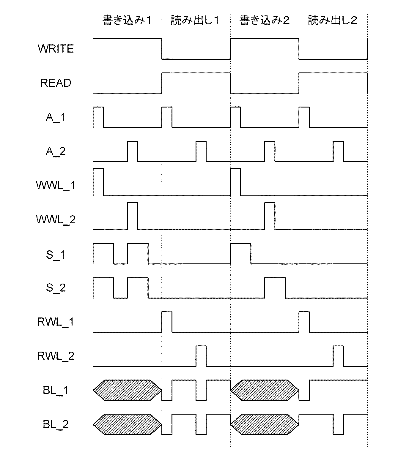
また、ノードAの電荷QAは、ノードAの電位VA、ノードAに接続される容量CA、定
数(const)を用いて、次式のように表される。ここで、ノードAに接続される容量
CAは、容量素子802の容量と他の容量の和である。
Further, the charge Q A of the node A is expressed by the following equation using the potential V A of the node A, the capacitance C A connected to the node A, and a constant (const). Here, the capacitance C A connected to the node A, is the sum of the capacity and other capacitance of the
ノードAの電流IAは、ノードAに流れ込む電荷(またはノードAから流れ出る電荷)の
時間微分であるから、ノードAの電流IAは次式のように表される。
Current I A of the node A, since the time derivative of charge flowing to the node A (or node A charge flowing from), the current I A of the node A is expressed by the following equation.
このように、ノードAに接続される容量CAと、出力端子の出力電位Voutから、ノー
ドAの電流IAを求めることができる。
Thus, the capacitor C A connected to the node A, the output potential Vout of the output terminal, it is possible to obtain a current I A of the node A.
以上に示す方法により、オフ状態においてトランジスタのソースとドレイン間を流れるリ
ーク電流(オフ電流)を測定することができる。
By the method described above, leakage current (off-state current) flowing between the source and drain of the transistor in the off state can be measured.
本実施例では、チャネル長L=10μm、チャネル幅W=50μmの、高純度化した酸化
物半導体を用いてトランジスタ804、トランジスタ805、トランジスタ806、トラ
ンジスタ808を作製した。また、並列された各測定系800において、容量素子802
の各容量値を、100fF、1pF、3pFとした。
In this example, the
The capacitance values were set to 100 fF, 1 pF, and 3 pF.
なお、本実施例に係る測定では、VDD=5V、VSS=0Vとした。また、測定期間に
おいては、電位V1を原則としてVSSとし、10secから300secの範囲ごとに
、100msecの期間だけVDDとしてVoutを測定した。また、素子に流れる電流
Iの算出に用いられるΔtは、約30000secとした。
In the measurement according to this example, VDD = 5V and VSS = 0V. Further, during the measurement period, Vout was measured by setting the potential V1 as VSS in principle and setting VDD as the VDD only for a period of 100 msec every range of 10 sec to 300 sec. Further, Δt used for calculation of the current I flowing through the element was about 30000 sec.
図21に、上記電流測定に係る経過時間Timeと、出力電位Voutとの関係を示す。
図21より、時間の経過にしたがって、電位が変化している様子が確認できる。
FIG. 21 shows the relationship between the elapsed time Time for the current measurement and the output potential Vout.
From FIG. 21, it can be confirmed that the potential changes as time passes.
図22には、上記電流測定によって算出された室温(25℃)におけるオフ電流を示す。
なお、図22は、ソース−ドレイン電圧Vと、オフ電流Iとの関係を表すものである。図
22から、ソース−ドレイン電圧が4Vの条件において、オフ電流は約40zA/μmで
あることが分かった。また、ソース−ドレイン電圧が3.1Vの条件において、オフ電流
は10zA/μm以下であることが分かった。なお、1zAは10−21Aを表す。
FIG. 22 shows the off-current at room temperature (25 ° C.) calculated by the current measurement.
FIG. 22 shows the relationship between the source-drain voltage V and the off-current I. From FIG. 22, it was found that the off-state current was about 40 zA / μm under the condition where the source-drain voltage was 4V. Further, it was found that the off-state current was 10 zA / μm or less under the condition where the source-drain voltage was 3.1V. Incidentally, 1 zA represents 10 -21 A.
さらに、上記電流測定によって算出された85℃の温度環境下におけるオフ電流について
図23に示す。図23は、85℃の温度環境下におけるソース−ドレイン電圧Vと、オフ
電流Iとの関係を表すものである。図23から、ソース−ドレイン電圧が3.1Vの条件
において、オフ電流は100zA/μm以下であることが分かった。
Furthermore, FIG. 23 shows the off-current in the temperature environment of 85 ° C. calculated by the current measurement. FIG. 23 shows the relationship between the source-drain voltage V and the off-current I under a temperature environment of 85 ° C. From FIG. 23, it was found that the off-state current was 100 zA / μm or less under the condition where the source-drain voltage was 3.1V.
以上、本実施例により、高純度化された酸化物半導体を用いたトランジスタでは、オフ電
流が十分に小さくなることが確認された。
As described above, according to this example, it was confirmed that the off-state current of the transistor including a highly purified oxide semiconductor is sufficiently small.
本実施例では、真性化された酸化物半導体を用いたトランジスタのオフ電流Ioffを詳
細に求めた結果について説明する。なお、計算には、sentaurus device
(synopsys社製TCADソフト)を用いた。また、キャリア再結合モデルとして
、SRHモデルおよびAuger再結合モデルを用いた。
In this example, a result of detailed determination of an off-state current Ioff of a transistor including an intrinsic oxide semiconductor will be described. For the calculation, the sentaurus device
(Synopsys TCAD software) was used. As the carrier recombination model, the SRH model and Auger recombination model were used.
計算に用いたトランジスタの構造は、図24のとおりである。図24に示すトランジスタ
562は、絶縁層543(材質:酸化珪素)と、ソース電極542aおよびドレイン電極
542b(材質:窒化チタン)と、上記絶縁層543の上面、ソース電極542aの上面
、およびドレイン電極542bの上面、の一部と接する酸化物半導体層544(材質:I
n−Ga−Zn−O系の酸化物半導体、厚さ:10nm)と、酸化物半導体層544を覆
うゲート絶縁層546(材質:酸化ハフニウム、厚さ:10nm)と、ゲート絶縁層54
6上のゲート電極548(材質:タングステン)と、を有する。なお、酸化物半導体はi
型と仮定し、ドナー密度Ndと真性キャリア密度niが等しいという条件の元で計算を行
った。
The structure of the transistor used for the calculation is as shown in FIG. A
an n-Ga-Zn-O-based oxide semiconductor (thickness: 10 nm); a gate insulating layer 546 (material: hafnium oxide; thickness: 10 nm) covering the
6 on the gate electrode 548 (material: tungsten). Note that an oxide semiconductor is i
The calculation was performed under the condition that the donor density Nd and the intrinsic carrier density ni are equal, assuming a mold.
チャネル長Lとしては、50nm、500nmの2条件を採用した。また、ソース電極5
42aとドレイン電極542bの間の電圧Vdsは、1Vとした。
As the channel length L, two conditions of 50 nm and 500 nm were adopted. The
The voltage Vds between 42a and the
計算に用いたパラメータは以下の通りである。
1.In−Ga−Zn−O系の酸化物半導体(酸化物半導体層の材料)
バンドギャップEg:3.15eV、電子親和力χ:4.3eV、比誘電率:15、電子
移動度:10cm2/Vs
2.窒化チタン(ソース電極およびドレイン電極の材料)
仕事関数φM:3.9eV
3.酸化ハフニウム(ゲート絶縁層の材料)
比誘電率:15
4.タングステン(ゲート電極の材料)
仕事関数φM:4.9eV
The parameters used for the calculation are as follows.
1. In-Ga-Zn-O-based oxide semiconductor (material of oxide semiconductor layer)
Band gap Eg: 3.15 eV, electron affinity χ: 4.3 eV, relative dielectric constant: 15, electron mobility: 10 cm 2 / Vs
2. Titanium nitride (source and drain electrode materials)
Work function φ M : 3.9 eV
3. Hafnium oxide (material for gate insulating layer)
Dielectric constant: 15
4). Tungsten (Gate electrode material)
Work function φ M : 4.9 eV
計算結果を図25に示す。図25において、横軸はゲート電圧VG(V)を、縦軸はドレ
イン電流ID(A/μm)を、それぞれ示している。また、図中、太い線がチャネル長L
=500nmの計算結果、細い線がチャネル長L=50nmの計算結果を、それぞれ示し
ている。
The calculation results are shown in FIG. In FIG. 25, the horizontal axis represents the gate voltage VG (V), and the vertical axis represents the drain current ID (A / μm). In the figure, the thick line is the channel length L.
= 500 nm calculation result, thin line shows calculation result of channel length L = 50 nm, respectively.
図25の計算結果により、チャネル長L=50nm、500nmの場合のいずれにおいて
も、オフ電流の下限値は10−29〜10−30(A/μm)と見積もられることがわか
る。
From the calculation results of FIG. 25, it can be seen that the lower limit of the off-current is estimated to be 10 −29 to 10 −30 (A / μm) in both cases where the channel length L = 50 nm and 500 nm.
なお、本実施例においては、図24に示すトップゲート構造のトランジスタを用いて、真
性化された酸化物半導体を用いたトランジスタのオフ電流を計算したが、ボトムゲート構
造などの異なる構造のトランジスタにおいてもほぼ同様のオフ電流が得られる。
Note that in this example, the off-state current of a transistor including an intrinsic oxide semiconductor was calculated using the top-gate transistor illustrated in FIG. 24; however, in a transistor having a different structure such as a bottom-gate structure, In this case, almost the same off-current can be obtained.
100 基板
102 保護層
104 半導体領域
106 素子分離絶縁層
108a ゲート絶縁層
108b ゲート絶縁層
110a ゲート電極
110b ゲート電極
116a チャネル形成領域
116b チャネル形成領域
120a 不純物領域
120b 不純物領域
120c 不純物領域
122 金属層
124a 金属化合物領域
124b 金属化合物領域
124c 金属化合物領域
130 絶縁層
142a ソース電極
142b ドレイン電極
142c 導電層
144 酸化物半導体層
146 ゲート絶縁層
148a ゲート電極
148b 電極
150 絶縁層
152 絶縁層
154 電極
156 配線
160 トランジスタ
162 トランジスタ
166 トランジスタ
168 容量素子
170 メモリセル
180 電位変換回路
190 第1の駆動回路
192 第2の駆動回路
202 制御回路
204 遅延回路
206 バッファ回路
208 読み出し回路
210 デコーダ
212 制御回路
214 昇圧用レベルシフタ
216 バッファ回路
218 バッファ回路
220 半導体層
222 半導体層
224 導電層
226 配線
240 導電層
242a ソース電極またはドレイン電極
242b ソース電極またはドレイン電極
242c ソース電極またはドレイン電極
542a ソース電極
542b ドレイン電極
543 絶縁層
544 酸化物半導体層
546 ゲート絶縁層
548 ゲート電極
562 トランジスタ
701 筐体
702 筐体
703 表示部
704 キーボード
711 本体
712 スタイラス
713 表示部
714 操作ボタン
715 外部インターフェイス
720 電子書籍
721 筐体
723 筐体
725 表示部
727 表示部
731 電源
733 操作キー
735 スピーカー
737 軸部
740 筐体
741 筐体
742 表示パネル
743 スピーカー
744 マイクロフォン
745 操作キー
746 ポインティングデバイス
747 カメラ用レンズ
748 外部接続端子
749 太陽電池セル
750 外部メモリスロット
761 本体
763 接眼部
764 操作スイッチ
765 表示部
766 バッテリー
767 表示部
770 テレビジョン装置
771 筐体
773 表示部
775 スタンド
780 リモコン操作機
800 測定系
802 容量素子
804 トランジスタ
805 トランジスタ
806 トランジスタ
808 トランジスタ
1200 第1のp型トランジスタ
1210 第2のp型トランジスタ
1220 第1のn型トランジスタ
1230 第3のp型トランジスタ
1240 第4のp型トランジスタ
1250 第2のn型トランジスタ
1260 第1のp型トランジスタ
1270 第1のn型トランジスタ
1280 第2のp型トランジスタ
1290 第2のn型トランジスタ
1300 第1のトランジスタ
1310 第2のトランジスタ
1320 第3のトランジスタ
1330 第4のトランジスタ
1340 第5のトランジスタ
1350 第1の容量素子
1360 第2の容量素子
1370 第3の容量素子
1380 第4の容量素子
1390 トランジスタ
100 substrate 102 protective layer 104 semiconductor region 106 element isolation insulating layer 108a gate insulating layer 108b gate insulating layer 110a gate electrode 110b gate electrode 116a channel forming region 116b channel forming region 120a impurity region 120b impurity region 120c impurity region 122 metal layer 124a metal compound Region 124b metal compound region 124c metal compound region 130 insulating layer 142a source electrode 142b drain electrode 142c conductive layer 144 oxide semiconductor layer 146 gate insulating layer 148a gate electrode 148b electrode 150 insulating layer 152 insulating layer 154 electrode 156 wiring 160 transistor 162 transistor 166 Transistor 168 Capacitance element 170 Memory cell 180 Potential conversion circuit 190 First drive circuit 192 Second drive circuit 202 Circuit 204 Delay circuit 206 Buffer circuit 208 Read circuit 210 Decoder 212 Control circuit 214 Boosting level shifter 216 Buffer circuit 218 Buffer circuit 220 Semiconductor layer 222 Semiconductor layer 224 Conductive layer 226 Wiring 240 Conductive layer 242a Source electrode or drain electrode 242b Source electrode or drain Electrode 242c Source or drain electrode 542a Source electrode 542b Drain electrode 543 Insulating layer 544 Oxide semiconductor layer 546 Gate insulating layer 548 Gate electrode 562 Transistor 701 Housing 702 Housing 703 Display portion 704 Keyboard 711 Main body 712 Stylus 713 Display portion 714 Operation Button 715 External interface 720 Electronic book 721 Case 723 Case 725 Display unit 727 Display unit 731 Power supply 733 Operation Key 735 Speaker 737 Shaft 740 Case 741 Case 742 Display panel 743 Speaker 744 Microphone 745 Operation key 746 Pointing device 747 Camera lens 748 External connection terminal 749 Solar cell 750 External memory slot 761 Main body 763 Eyepiece 764 Operation switch 765 Display unit 766 Battery 767 Display unit 770 Television device 771 Case 773 Display unit 775 Stand 780 Remote control device 800 Measurement system 802 Capacitance element 804 Transistor 805 Transistor 806 Transistor 808 Transistor 1200 First p-type transistor 1210 Second p Type transistor 1220 first n-type transistor 1230 third p-type transistor 1240 fourth p-type transistor 1250 second n-type transistor 1260 first p-type transistor 1270 first n-type transistor 1280 second p-type transistor 1290 second n-type transistor 1300 first transistor 1310 second transistor 1320 third transistor 1330 fourth transistor Transistor 1340 Fifth transistor 1350 First capacitor 1360 Second capacitor 1370 Third capacitor 1380 Fourth capacitor 1390 Transistor
Claims (3)
前記第1のトランジスタのゲートは、前記第3のトランジスタのソースまたはドレインの一方と電気的に接続され、
前記第1のトランジスタのゲートは、前記容量素子の一方の電極と電気的に接続され、
前記第1のトランジスタのソースまたはドレインの一方は、前記第2のトランジスタのソースまたはドレインの一方と電気的に接続され、
前記第1のトランジスタのソースまたはドレインの他方は、前記第1の配線と電気的に接続され、
前記容量素子の他方の電極は、前記第1の配線と電気的に接続され、
前記第3のトランジスタは、酸化物半導体を含むチャネル形成領域を有し、
前記第1のトランジスタのゲートに、異なる三つまたはそれ以上の電位が与えられることを特徴とする半導体装置。 First to third transistors, a capacitor, and a first wiring;
A gate of the first transistor is electrically connected to one of a source and a drain of the third transistor;
A gate of the first transistor is electrically connected to one electrode of the capacitor;
One of the source and the drain of the first transistor is electrically connected to one of the source and the drain of the second transistor;
The other of the source and the drain of the first transistor is electrically connected to the first wiring;
The other electrode of the capacitive element is electrically connected to the first wiring;
The third transistor includes a channel formation region including an oxide semiconductor;
3. A semiconductor device, wherein three or more different potentials are applied to the gate of the first transistor.
前記第1のトランジスタのゲートは、前記第3のトランジスタのソースまたはドレインの一方と電気的に接続され、
前記第1のトランジスタのゲートは、前記容量素子の一方の電極と電気的に接続され、
前記第1のトランジスタのソースまたはドレインの一方は、前記第2のトランジスタのソースまたはドレインの一方と電気的に接続され、
前記第1のトランジスタのソースまたはドレインの他方は、前記第1の配線と電気的に接続され、
前記容量素子の他方の電極は、前記第2の配線と電気的に接続され、
前記第3のトランジスタは、酸化物半導体を含むチャネル形成領域を有し、
前記第1のトランジスタのゲートに、異なる三つまたはそれ以上の電位が与えられることを特徴とする半導体装置。 Having first to third transistors, a capacitor, a first wiring, and a second wiring;
A gate of the first transistor is electrically connected to one of a source and a drain of the third transistor;
A gate of the first transistor is electrically connected to one electrode of the capacitor;
One of the source and the drain of the first transistor is electrically connected to one of the source and the drain of the second transistor;
The other of the source and the drain of the first transistor is electrically connected to the first wiring;
The other electrode of the capacitive element is electrically connected to the second wiring;
The third transistor includes a channel formation region including an oxide semiconductor;
3. A semiconductor device, wherein three or more different potentials are applied to the gate of the first transistor.
前記第1のトランジスタは、シリコンを含むチャネル形成領域を有し、
前記第2のトランジスタは、シリコンを含むチャネル形成領域を有することを特徴とする半導体装置。 In claim 1 or claim 2,
The first transistor has a channel formation region containing silicon,
The semiconductor device, wherein the second transistor has a channel formation region containing silicon.
Priority Applications (1)
| Application Number | Priority Date | Filing Date | Title |
|---|---|---|---|
| JP2015120001A JP2015201250A (en) | 2010-04-16 | 2015-06-15 | semiconductor device |
Applications Claiming Priority (3)
| Application Number | Priority Date | Filing Date | Title |
|---|---|---|---|
| JP2010095196 | 2010-04-16 | ||
| JP2010095196 | 2010-04-16 | ||
| JP2015120001A JP2015201250A (en) | 2010-04-16 | 2015-06-15 | semiconductor device |
Related Parent Applications (1)
| Application Number | Title | Priority Date | Filing Date |
|---|---|---|---|
| JP2011088799A Division JP5764370B2 (en) | 2010-04-16 | 2011-04-13 | Semiconductor device |
Publications (1)
| Publication Number | Publication Date |
|---|---|
| JP2015201250A true JP2015201250A (en) | 2015-11-12 |
Family
ID=44788088
Family Applications (3)
| Application Number | Title | Priority Date | Filing Date |
|---|---|---|---|
| JP2011088799A Expired - Fee Related JP5764370B2 (en) | 2010-04-16 | 2011-04-13 | Semiconductor device |
| JP2013104197A Expired - Fee Related JP5604560B2 (en) | 2010-04-16 | 2013-05-16 | Semiconductor device |
| JP2015120001A Withdrawn JP2015201250A (en) | 2010-04-16 | 2015-06-15 | semiconductor device |
Family Applications Before (2)
| Application Number | Title | Priority Date | Filing Date |
|---|---|---|---|
| JP2011088799A Expired - Fee Related JP5764370B2 (en) | 2010-04-16 | 2011-04-13 | Semiconductor device |
| JP2013104197A Expired - Fee Related JP5604560B2 (en) | 2010-04-16 | 2013-05-16 | Semiconductor device |
Country Status (5)
| Country | Link |
|---|---|
| US (1) | US8411480B2 (en) |
| JP (3) | JP5764370B2 (en) |
| KR (1) | KR101904445B1 (en) |
| TW (1) | TWI517157B (en) |
| WO (1) | WO2011129233A1 (en) |
Cited By (1)
| Publication number | Priority date | Publication date | Assignee | Title |
|---|---|---|---|---|
| JP2017117508A (en) * | 2015-12-22 | 2017-06-29 | 株式会社半導体エネルギー研究所 | Semiconductor device, display panel, and electronic device |
Families Citing this family (48)
| Publication number | Priority date | Publication date | Assignee | Title |
|---|---|---|---|---|
| WO2011058934A1 (en) | 2009-11-13 | 2011-05-19 | Semiconductor Energy Laboratory Co., Ltd. | Semiconductor device and driving method thereof |
| CN102754162B (en) * | 2010-02-19 | 2015-12-09 | 株式会社半导体能源研究所 | The driving method of semiconductor devices and semiconductor devices |
| KR101891065B1 (en) * | 2010-03-19 | 2018-08-24 | 가부시키가이샤 한도오따이 에네루기 켄큐쇼 | Semiconductor device and driving method of semiconductor device |
| KR101884031B1 (en) * | 2010-04-07 | 2018-07-31 | 가부시키가이샤 한도오따이 에네루기 켄큐쇼 | Semiconductor memory device |
| WO2011129233A1 (en) * | 2010-04-16 | 2011-10-20 | Semiconductor Energy Laboratory Co., Ltd. | Semiconductor device |
| JP5923248B2 (en) | 2010-05-20 | 2016-05-24 | 株式会社半導体エネルギー研究所 | Semiconductor device |
| US8779433B2 (en) | 2010-06-04 | 2014-07-15 | Semiconductor Energy Laboratory Co., Ltd. | Semiconductor device |
| US8422272B2 (en) | 2010-08-06 | 2013-04-16 | Semiconductor Energy Laboratory Co., Ltd. | Semiconductor device and driving method thereof |
| US8582348B2 (en) | 2010-08-06 | 2013-11-12 | Semiconductor Energy Laboratory Co., Ltd. | Semiconductor device and method for driving semiconductor device |
| US8467231B2 (en) | 2010-08-06 | 2013-06-18 | Semiconductor Energy Laboratory Co., Ltd. | Semiconductor device and driving method thereof |
| US8634228B2 (en) * | 2010-09-02 | 2014-01-21 | Semiconductor Energy Laboratory Co., Ltd. | Driving method of semiconductor device |
| JP5852874B2 (en) | 2010-12-28 | 2016-02-03 | 株式会社半導体エネルギー研究所 | Semiconductor device |
| JP6013682B2 (en) | 2011-05-20 | 2016-10-25 | 株式会社半導体エネルギー研究所 | Driving method of semiconductor device |
| JP6013685B2 (en) | 2011-07-22 | 2016-10-25 | 株式会社半導体エネルギー研究所 | Semiconductor device |
| TWI580047B (en) * | 2011-12-23 | 2017-04-21 | 半導體能源研究所股份有限公司 | Semiconductor device |
| TWI536388B (en) * | 2012-01-12 | 2016-06-01 | Sharp Kk | Semiconductor memory circuits and devices |
| KR102097171B1 (en) * | 2012-01-20 | 2020-04-03 | 가부시키가이샤 한도오따이 에네루기 켄큐쇼 | Semiconductor device |
| US9287370B2 (en) * | 2012-03-02 | 2016-03-15 | Semiconductor Energy Laboratory Co., Ltd. | Memory device comprising a transistor including an oxide semiconductor and semiconductor device including the same |
| CN104321967B (en) * | 2012-05-25 | 2018-01-09 | 株式会社半导体能源研究所 | Programmable logic device and semiconductor device |
| US9054678B2 (en) * | 2012-07-06 | 2015-06-09 | Semiconductor Energy Laboratory Co., Ltd. | Semiconductor device and driving method thereof |
| KR102107591B1 (en) * | 2012-07-18 | 2020-05-07 | 가부시키가이샤 한도오따이 에네루기 켄큐쇼 | Memory element and programmable logic device |
| KR102112364B1 (en) * | 2012-12-06 | 2020-05-18 | 가부시키가이샤 한도오따이 에네루기 켄큐쇼 | Semiconductor device |
| WO2014142043A1 (en) | 2013-03-14 | 2014-09-18 | Semiconductor Energy Laboratory Co., Ltd. | Method for driving semiconductor device and semiconductor device |
| WO2014142332A1 (en) | 2013-03-14 | 2014-09-18 | Semiconductor Energy Laboratory Co., Ltd. | Method for driving semiconductor device and semiconductor device |
| WO2014157019A1 (en) * | 2013-03-25 | 2014-10-02 | Semiconductor Energy Laboratory Co., Ltd. | Semiconductor device |
| TWI618081B (en) | 2013-05-30 | 2018-03-11 | 半導體能源研究所股份有限公司 | Driving method of semiconductor device |
| US9515094B2 (en) * | 2013-06-26 | 2016-12-06 | Semiconductor Energy Laboratory Co., Ltd. | Storage device and semiconductor device |
| WO2015060133A1 (en) * | 2013-10-22 | 2015-04-30 | Semiconductor Energy Laboratory Co., Ltd. | Semiconductor device |
| JP6478562B2 (en) | 2013-11-07 | 2019-03-06 | 株式会社半導体エネルギー研究所 | Semiconductor device |
| US10055232B2 (en) * | 2014-02-07 | 2018-08-21 | Semiconductor Energy Laboratory Co., Ltd. | Semiconductor device comprising memory circuit |
| US9479175B2 (en) * | 2014-02-07 | 2016-10-25 | Semiconductor Energy Laboratory Co., Ltd. | Semiconductor device and electronic device |
| WO2015118436A1 (en) | 2014-02-07 | 2015-08-13 | Semiconductor Energy Laboratory Co., Ltd. | Semiconductor device, device, and electronic device |
| JP2015172991A (en) * | 2014-02-21 | 2015-10-01 | 株式会社半導体エネルギー研究所 | Semiconductor device, electronic component, and electronic device |
| JP6560508B2 (en) * | 2014-03-13 | 2019-08-14 | 株式会社半導体エネルギー研究所 | Semiconductor device |
| US9716100B2 (en) * | 2014-03-14 | 2017-07-25 | Semiconductor Energy Laboratory Co., Ltd. | Semiconductor device, method for driving semiconductor device, and electronic device |
| WO2015170220A1 (en) * | 2014-05-09 | 2015-11-12 | Semiconductor Energy Laboratory Co., Ltd. | Memory device and electronic device |
| JP6552336B2 (en) | 2014-08-29 | 2019-07-31 | 株式会社半導体エネルギー研究所 | Semiconductor device |
| TWI691088B (en) * | 2014-11-21 | 2020-04-11 | 日商半導體能源研究所股份有限公司 | Semiconductor device |
| US9424890B2 (en) | 2014-12-01 | 2016-08-23 | Semiconductor Energy Laboratory Co., Ltd. | Semiconductor device and driving method thereof |
| JP6667267B2 (en) | 2014-12-08 | 2020-03-18 | 株式会社半導体エネルギー研究所 | Semiconductor device |
| WO2016092416A1 (en) * | 2014-12-11 | 2016-06-16 | Semiconductor Energy Laboratory Co., Ltd. | Semiconductor device, memory device, and electronic device |
| US9293207B1 (en) * | 2015-02-03 | 2016-03-22 | Freescale Semiconductor, Inc. | Embedded data and code non-volatile memory cell configurations |
| KR20160117222A (en) | 2015-03-30 | 2016-10-10 | 가부시키가이샤 한도오따이 에네루기 켄큐쇼 | Test method of semiconductor device |
| US9589611B2 (en) * | 2015-04-01 | 2017-03-07 | Semiconductor Energy Laboratory Co., Ltd. | Memory device, semiconductor device, and electronic device |
| WO2017130082A1 (en) | 2016-01-29 | 2017-08-03 | Semiconductor Energy Laboratory Co., Ltd. | Semiconductor device, electronic component, and electronic device |
| JP6995481B2 (en) | 2016-01-29 | 2022-02-04 | 株式会社半導体エネルギー研究所 | Source driver |
| US10490116B2 (en) | 2016-07-06 | 2019-11-26 | Semiconductor Energy Laboratory Co., Ltd. | Semiconductor device, memory device, and display system |
| KR20240006569A (en) * | 2021-05-10 | 2024-01-15 | 가부시키가이샤 한도오따이 에네루기 켄큐쇼 | semiconductor device |
Citations (5)
| Publication number | Priority date | Publication date | Assignee | Title |
|---|---|---|---|---|
| JPS62274773A (en) * | 1986-05-23 | 1987-11-28 | Hitachi Ltd | Semiconductor memory |
| JPH07211084A (en) * | 1994-01-18 | 1995-08-11 | Sunao Shibata | Semiconductor device |
| US20070159894A1 (en) * | 2005-06-27 | 2007-07-12 | Infineon Technologies Ag | Memory cell, read device for memory cell, memory assembly, and corresponding method |
| JP2010062229A (en) * | 2008-09-01 | 2010-03-18 | Semiconductor Energy Lab Co Ltd | Thin-film transistor and method of manufacturing the same |
| US20110101339A1 (en) * | 2009-10-30 | 2011-05-05 | Semiconductor Energy Laboratory Co., Ltd. | Semiconductor device |
Family Cites Families (116)
| Publication number | Priority date | Publication date | Assignee | Title |
|---|---|---|---|---|
| EP0053878B1 (en) | 1980-12-08 | 1985-08-14 | Kabushiki Kaisha Toshiba | Semiconductor memory device |
| JP3227917B2 (en) * | 1993-07-26 | 2001-11-12 | ソニー株式会社 | Memory cell for amplification type DRAM and method of manufacturing the same |
| JPH08321182A (en) * | 1995-05-23 | 1996-12-03 | Nippon Telegr & Teleph Corp <Ntt> | Semiconductor memory |
| JPH11505377A (en) | 1995-08-03 | 1999-05-18 | フィリップス エレクトロニクス ネムローゼ フェンノートシャップ | Semiconductor device |
| JP3625598B2 (en) | 1995-12-30 | 2005-03-02 | 三星電子株式会社 | Manufacturing method of liquid crystal display device |
| JP4103968B2 (en) | 1996-09-18 | 2008-06-18 | 株式会社半導体エネルギー研究所 | Insulated gate type semiconductor device |
| JPH11126491A (en) * | 1997-08-20 | 1999-05-11 | Fujitsu Ltd | Semiconductor storage device |
| JP4170454B2 (en) | 1998-07-24 | 2008-10-22 | Hoya株式会社 | Article having transparent conductive oxide thin film and method for producing the same |
| JP2000150861A (en) | 1998-11-16 | 2000-05-30 | Tdk Corp | Oxide thin film |
| JP3276930B2 (en) | 1998-11-17 | 2002-04-22 | 科学技術振興事業団 | Transistor and semiconductor device |
| JP3955409B2 (en) * | 1999-03-17 | 2007-08-08 | 株式会社ルネサステクノロジ | Semiconductor memory device |
| TW460731B (en) | 1999-09-03 | 2001-10-21 | Ind Tech Res Inst | Electrode structure and production method of wide viewing angle LCD |
| JP4089858B2 (en) | 2000-09-01 | 2008-05-28 | 国立大学法人東北大学 | Semiconductor device |
| KR20020038482A (en) | 2000-11-15 | 2002-05-23 | 모리시타 요이찌 | Thin film transistor array, method for producing the same, and display panel using the same |
| JP3997731B2 (en) | 2001-03-19 | 2007-10-24 | 富士ゼロックス株式会社 | Method for forming a crystalline semiconductor thin film on a substrate |
| JP2002289859A (en) | 2001-03-23 | 2002-10-04 | Minolta Co Ltd | Thin film transistor |
| JP2002368226A (en) * | 2001-06-11 | 2002-12-20 | Sharp Corp | Semiconductor device, semiconductor storage device and manufacturing method thereof, and portable information device |
| JP2003017591A (en) * | 2001-07-03 | 2003-01-17 | Hitachi Ltd | Semiconductor storage device |
| JP3925839B2 (en) | 2001-09-10 | 2007-06-06 | シャープ株式会社 | Semiconductor memory device and test method thereof |
| JP4090716B2 (en) | 2001-09-10 | 2008-05-28 | 雅司 川崎 | Thin film transistor and matrix display device |
| JP4164562B2 (en) | 2002-09-11 | 2008-10-15 | 独立行政法人科学技術振興機構 | Transparent thin film field effect transistor using homologous thin film as active layer |
| EP1443130B1 (en) | 2001-11-05 | 2011-09-28 | Japan Science and Technology Agency | Natural superlattice homologous single crystal thin film, method for preparation thereof, and device using said single crystal thin film |
| JP4083486B2 (en) | 2002-02-21 | 2008-04-30 | 独立行政法人科学技術振興機構 | Method for producing LnCuO (S, Se, Te) single crystal thin film |
| US7049190B2 (en) | 2002-03-15 | 2006-05-23 | Sanyo Electric Co., Ltd. | Method for forming ZnO film, method for forming ZnO semiconductor layer, method for fabricating semiconductor device, and semiconductor device |
| JP3933591B2 (en) | 2002-03-26 | 2007-06-20 | 淳二 城戸 | Organic electroluminescent device |
| JP4278338B2 (en) * | 2002-04-01 | 2009-06-10 | 株式会社ルネサステクノロジ | Semiconductor memory device |
| US7339187B2 (en) | 2002-05-21 | 2008-03-04 | State Of Oregon Acting By And Through The Oregon State Board Of Higher Education On Behalf Of Oregon State University | Transistor structures |
| US6787835B2 (en) | 2002-06-11 | 2004-09-07 | Hitachi, Ltd. | Semiconductor memories |
| JP2004022625A (en) | 2002-06-13 | 2004-01-22 | Murata Mfg Co Ltd | Semiconductor device and method of manufacturing the semiconductor device |
| US7105868B2 (en) | 2002-06-24 | 2006-09-12 | Cermet, Inc. | High-electron mobility transistor with zinc oxide |
| US7067843B2 (en) | 2002-10-11 | 2006-06-27 | E. I. Du Pont De Nemours And Company | Transparent oxide semiconductor thin film transistors |
| DE10248722A1 (en) * | 2002-10-18 | 2004-05-06 | Infineon Technologies Ag | Integrated circuit arrangement with capacitor and manufacturing process |
| JP4166105B2 (en) | 2003-03-06 | 2008-10-15 | シャープ株式会社 | Semiconductor device and manufacturing method thereof |
| JP2004273732A (en) | 2003-03-07 | 2004-09-30 | Sharp Corp | Active matrix substrate and manufacturing method thereof |
| JP4108633B2 (en) | 2003-06-20 | 2008-06-25 | シャープ株式会社 | THIN FILM TRANSISTOR, MANUFACTURING METHOD THEREOF, AND ELECTRONIC DEVICE |
| US7262463B2 (en) | 2003-07-25 | 2007-08-28 | Hewlett-Packard Development Company, L.P. | Transistor including a deposited channel region having a doped portion |
| DE10344604B4 (en) * | 2003-09-25 | 2011-08-11 | Infineon Technologies AG, 81669 | Storage unit with collecting electrodes |
| US7297977B2 (en) | 2004-03-12 | 2007-11-20 | Hewlett-Packard Development Company, L.P. | Semiconductor device |
| US7282782B2 (en) | 2004-03-12 | 2007-10-16 | Hewlett-Packard Development Company, L.P. | Combined binary oxide semiconductor device |
| EP1737044B1 (en) * | 2004-03-12 | 2014-12-10 | Japan Science and Technology Agency | Amorphous oxide and thin film transistor |
| US7145174B2 (en) | 2004-03-12 | 2006-12-05 | Hewlett-Packard Development Company, Lp. | Semiconductor device |
| US7211825B2 (en) | 2004-06-14 | 2007-05-01 | Yi-Chi Shih | Indium oxide-based thin film transistors and circuits |
| JP4927321B2 (en) * | 2004-06-22 | 2012-05-09 | ルネサスエレクトロニクス株式会社 | Semiconductor memory device |
| JP2006100760A (en) | 2004-09-02 | 2006-04-13 | Casio Comput Co Ltd | Thin film transistor and manufacturing method thereof |
| US7285501B2 (en) | 2004-09-17 | 2007-10-23 | Hewlett-Packard Development Company, L.P. | Method of forming a solution processed device |
| US7298084B2 (en) | 2004-11-02 | 2007-11-20 | 3M Innovative Properties Company | Methods and displays utilizing integrated zinc oxide row and column drivers in conjunction with organic light emitting diodes |
| RU2358354C2 (en) | 2004-11-10 | 2009-06-10 | Кэнон Кабусики Кайся | Light-emitting device |
| KR100998527B1 (en) | 2004-11-10 | 2010-12-07 | 고쿠리츠다이가쿠호진 토쿄고교 다이가꾸 | Amorphous oxide and field effect transistor |
| US7829444B2 (en) | 2004-11-10 | 2010-11-09 | Canon Kabushiki Kaisha | Field effect transistor manufacturing method |
| US7791072B2 (en) | 2004-11-10 | 2010-09-07 | Canon Kabushiki Kaisha | Display |
| EP1815530B1 (en) | 2004-11-10 | 2021-02-17 | Canon Kabushiki Kaisha | Field effect transistor employing an amorphous oxide |
| US7863611B2 (en) | 2004-11-10 | 2011-01-04 | Canon Kabushiki Kaisha | Integrated circuits utilizing amorphous oxides |
| US7453065B2 (en) | 2004-11-10 | 2008-11-18 | Canon Kabushiki Kaisha | Sensor and image pickup device |
| US7579224B2 (en) | 2005-01-21 | 2009-08-25 | Semiconductor Energy Laboratory Co., Ltd. | Method for manufacturing a thin film semiconductor device |
| TWI505473B (en) | 2005-01-28 | 2015-10-21 | 半導體能源研究所股份有限公司 | Semiconductor device, electronic device, and method of manufacturing semiconductor device |
| TWI481024B (en) | 2005-01-28 | 2015-04-11 | 半導體能源研究所股份有限公司 | Semiconductor device, electronic device, and method of manufacturing semiconductor device |
| US7858451B2 (en) | 2005-02-03 | 2010-12-28 | Semiconductor Energy Laboratory Co., Ltd. | Electronic device, semiconductor device and manufacturing method thereof |
| US7948171B2 (en) | 2005-02-18 | 2011-05-24 | Semiconductor Energy Laboratory Co., Ltd. | Light emitting device |
| US20060197092A1 (en) | 2005-03-03 | 2006-09-07 | Randy Hoffman | System and method for forming conductive material on a substrate |
| US8681077B2 (en) | 2005-03-18 | 2014-03-25 | Semiconductor Energy Laboratory Co., Ltd. | Semiconductor device, and display device, driving method and electronic apparatus thereof |
| US7544967B2 (en) | 2005-03-28 | 2009-06-09 | Massachusetts Institute Of Technology | Low voltage flexible organic/transparent transistor for selective gas sensing, photodetecting and CMOS device applications |
| US7645478B2 (en) | 2005-03-31 | 2010-01-12 | 3M Innovative Properties Company | Methods of making displays |
| US8300031B2 (en) | 2005-04-20 | 2012-10-30 | Semiconductor Energy Laboratory Co., Ltd. | Semiconductor device comprising transistor having gate and drain connected through a current-voltage conversion element |
| JP2006344849A (en) | 2005-06-10 | 2006-12-21 | Casio Comput Co Ltd | Thin film transistor |
| US7691666B2 (en) | 2005-06-16 | 2010-04-06 | Eastman Kodak Company | Methods of making thin film transistors comprising zinc-oxide-based semiconductor materials and transistors made thereby |
| US7402506B2 (en) | 2005-06-16 | 2008-07-22 | Eastman Kodak Company | Methods of making thin film transistors comprising zinc-oxide-based semiconductor materials and transistors made thereby |
| US7507618B2 (en) | 2005-06-27 | 2009-03-24 | 3M Innovative Properties Company | Method for making electronic devices using metal oxide nanoparticles |
| KR100711890B1 (en) | 2005-07-28 | 2007-04-25 | 삼성에스디아이 주식회사 | OLED display and manufacturing method thereof |
| JP2007059128A (en) | 2005-08-23 | 2007-03-08 | Canon Inc | Organic EL display device and manufacturing method thereof |
| JP4280736B2 (en) | 2005-09-06 | 2009-06-17 | キヤノン株式会社 | Semiconductor element |
| JP2007073705A (en) | 2005-09-06 | 2007-03-22 | Canon Inc | Oxide semiconductor channel thin film transistor and method for manufacturing the same |
| JP5116225B2 (en) | 2005-09-06 | 2013-01-09 | キヤノン株式会社 | Manufacturing method of oxide semiconductor device |
| JP4850457B2 (en) | 2005-09-06 | 2012-01-11 | キヤノン株式会社 | Thin film transistor and thin film diode |
| JP4560502B2 (en) * | 2005-09-06 | 2010-10-13 | キヤノン株式会社 | Field effect transistor |
| EP1998373A3 (en) | 2005-09-29 | 2012-10-31 | Semiconductor Energy Laboratory Co, Ltd. | Semiconductor device having oxide semiconductor layer and manufacturing method thereof |
| JP5037808B2 (en) | 2005-10-20 | 2012-10-03 | キヤノン株式会社 | Field effect transistor using amorphous oxide, and display device using the transistor |
| CN101577231B (en) | 2005-11-15 | 2013-01-02 | 株式会社半导体能源研究所 | Semiconductor device and method of manufacturing the same |
| TWI292281B (en) | 2005-12-29 | 2008-01-01 | Ind Tech Res Inst | Pixel structure of active organic light emitting diode and method of fabricating the same |
| US7867636B2 (en) | 2006-01-11 | 2011-01-11 | Murata Manufacturing Co., Ltd. | Transparent conductive film and method for manufacturing the same |
| JP4977478B2 (en) | 2006-01-21 | 2012-07-18 | 三星電子株式会社 | ZnO film and method of manufacturing TFT using the same |
| US7576394B2 (en) | 2006-02-02 | 2009-08-18 | Kochi Industrial Promotion Center | Thin film transistor including low resistance conductive thin films and manufacturing method thereof |
| US7977169B2 (en) | 2006-02-15 | 2011-07-12 | Kochi Industrial Promotion Center | Semiconductor device including active layer made of zinc oxide with controlled orientations and manufacturing method thereof |
| KR20070101595A (en) | 2006-04-11 | 2007-10-17 | 삼성전자주식회사 | ZnO TFT |
| US20070252928A1 (en) | 2006-04-28 | 2007-11-01 | Toppan Printing Co., Ltd. | Structure, transmission type liquid crystal display, reflection type display and manufacturing method thereof |
| JP5028033B2 (en) | 2006-06-13 | 2012-09-19 | キヤノン株式会社 | Oxide semiconductor film dry etching method |
| JP4609797B2 (en) | 2006-08-09 | 2011-01-12 | Nec液晶テクノロジー株式会社 | Thin film device and manufacturing method thereof |
| JP4999400B2 (en) | 2006-08-09 | 2012-08-15 | キヤノン株式会社 | Oxide semiconductor film dry etching method |
| JP4332545B2 (en) | 2006-09-15 | 2009-09-16 | キヤノン株式会社 | Field effect transistor and manufacturing method thereof |
| JP5164357B2 (en) | 2006-09-27 | 2013-03-21 | キヤノン株式会社 | Semiconductor device and manufacturing method of semiconductor device |
| JP4274219B2 (en) | 2006-09-27 | 2009-06-03 | セイコーエプソン株式会社 | Electronic devices, organic electroluminescence devices, organic thin film semiconductor devices |
| US7622371B2 (en) | 2006-10-10 | 2009-11-24 | Hewlett-Packard Development Company, L.P. | Fused nanocrystal thin film semiconductor and method |
| US7772021B2 (en) | 2006-11-29 | 2010-08-10 | Samsung Electronics Co., Ltd. | Flat panel displays comprising a thin-film transistor having a semiconductive oxide in its channel and methods of fabricating the same for use in flat panel displays |
| JP2008140684A (en) | 2006-12-04 | 2008-06-19 | Toppan Printing Co Ltd | Color EL display and manufacturing method thereof |
| KR101303578B1 (en) | 2007-01-05 | 2013-09-09 | 삼성전자주식회사 | Etching method of thin film |
| US8207063B2 (en) | 2007-01-26 | 2012-06-26 | Eastman Kodak Company | Process for atomic layer deposition |
| KR100851215B1 (en) | 2007-03-14 | 2008-08-07 | 삼성에스디아이 주식회사 | Thin film transistor and organic light emitting display device using same |
| US7795613B2 (en) | 2007-04-17 | 2010-09-14 | Toppan Printing Co., Ltd. | Structure with transistor |
| KR101325053B1 (en) | 2007-04-18 | 2013-11-05 | 삼성디스플레이 주식회사 | Thin film transistor substrate and manufacturing method thereof |
| KR20080094300A (en) | 2007-04-19 | 2008-10-23 | 삼성전자주식회사 | Thin film transistors and methods of manufacturing the same and flat panel displays comprising thin film transistors |
| KR101334181B1 (en) | 2007-04-20 | 2013-11-28 | 삼성전자주식회사 | Thin Film Transistor having selectively crystallized channel layer and method of manufacturing the same |
| WO2008133345A1 (en) | 2007-04-25 | 2008-11-06 | Canon Kabushiki Kaisha | Oxynitride semiconductor |
| KR101345376B1 (en) | 2007-05-29 | 2013-12-24 | 삼성전자주식회사 | Fabrication method of ZnO family Thin film transistor |
| US8202365B2 (en) | 2007-12-17 | 2012-06-19 | Fujifilm Corporation | Process for producing oriented inorganic crystalline film, and semiconductor device using the oriented inorganic crystalline film |
| JP2009206508A (en) * | 2008-01-31 | 2009-09-10 | Canon Inc | Thin film transistor and display |
| JP5305696B2 (en) * | 2008-03-06 | 2013-10-02 | キヤノン株式会社 | Semiconductor device processing method |
| JP2010003910A (en) * | 2008-06-20 | 2010-01-07 | Toshiba Mobile Display Co Ltd | Display element |
| JP4623179B2 (en) | 2008-09-18 | 2011-02-02 | ソニー株式会社 | Thin film transistor and manufacturing method thereof |
| JP5451280B2 (en) | 2008-10-09 | 2014-03-26 | キヤノン株式会社 | Wurtzite crystal growth substrate, manufacturing method thereof, and semiconductor device |
| JP5781720B2 (en) | 2008-12-15 | 2015-09-24 | ルネサスエレクトロニクス株式会社 | Semiconductor device and manufacturing method of semiconductor device |
| CN102612741B (en) * | 2009-11-06 | 2014-11-12 | 株式会社半导体能源研究所 | Semiconductor device |
| CN102754162B (en) * | 2010-02-19 | 2015-12-09 | 株式会社半导体能源研究所 | The driving method of semiconductor devices and semiconductor devices |
| WO2011102233A1 (en) * | 2010-02-19 | 2011-08-25 | Semiconductor Energy Laboratory Co., Ltd. | Semiconductor device |
| WO2011129233A1 (en) * | 2010-04-16 | 2011-10-20 | Semiconductor Energy Laboratory Co., Ltd. | Semiconductor device |
| US8467231B2 (en) * | 2010-08-06 | 2013-06-18 | Semiconductor Energy Laboratory Co., Ltd. | Semiconductor device and driving method thereof |
| US9048142B2 (en) * | 2010-12-28 | 2015-06-02 | Semiconductor Energy Laboratory Co., Ltd. | Semiconductor device |
| JP5898527B2 (en) * | 2011-03-04 | 2016-04-06 | 株式会社半導体エネルギー研究所 | Semiconductor device |
-
2011
- 2011-03-30 WO PCT/JP2011/058661 patent/WO2011129233A1/en not_active Ceased
- 2011-03-30 KR KR1020127029488A patent/KR101904445B1/en not_active Expired - Fee Related
- 2011-04-08 US US13/082,464 patent/US8411480B2/en active Active
- 2011-04-13 JP JP2011088799A patent/JP5764370B2/en not_active Expired - Fee Related
- 2011-04-13 TW TW100112807A patent/TWI517157B/en not_active IP Right Cessation
-
2013
- 2013-05-16 JP JP2013104197A patent/JP5604560B2/en not_active Expired - Fee Related
-
2015
- 2015-06-15 JP JP2015120001A patent/JP2015201250A/en not_active Withdrawn
Patent Citations (6)
| Publication number | Priority date | Publication date | Assignee | Title |
|---|---|---|---|---|
| JPS62274773A (en) * | 1986-05-23 | 1987-11-28 | Hitachi Ltd | Semiconductor memory |
| JPH07211084A (en) * | 1994-01-18 | 1995-08-11 | Sunao Shibata | Semiconductor device |
| US20070159894A1 (en) * | 2005-06-27 | 2007-07-12 | Infineon Technologies Ag | Memory cell, read device for memory cell, memory assembly, and corresponding method |
| JP2010062229A (en) * | 2008-09-01 | 2010-03-18 | Semiconductor Energy Lab Co Ltd | Thin-film transistor and method of manufacturing the same |
| US20110101339A1 (en) * | 2009-10-30 | 2011-05-05 | Semiconductor Energy Laboratory Co., Ltd. | Semiconductor device |
| JP2011119675A (en) * | 2009-10-30 | 2011-06-16 | Semiconductor Energy Lab Co Ltd | Semiconductor device |
Cited By (1)
| Publication number | Priority date | Publication date | Assignee | Title |
|---|---|---|---|---|
| JP2017117508A (en) * | 2015-12-22 | 2017-06-29 | 株式会社半導体エネルギー研究所 | Semiconductor device, display panel, and electronic device |
Also Published As
| Publication number | Publication date |
|---|---|
| KR101904445B1 (en) | 2018-10-04 |
| JP2011238334A (en) | 2011-11-24 |
| TWI517157B (en) | 2016-01-11 |
| JP5764370B2 (en) | 2015-08-19 |
| KR20130056240A (en) | 2013-05-29 |
| JP5604560B2 (en) | 2014-10-08 |
| US20110255325A1 (en) | 2011-10-20 |
| JP2013211091A (en) | 2013-10-10 |
| US8411480B2 (en) | 2013-04-02 |
| WO2011129233A1 (en) | 2011-10-20 |
| TW201142848A (en) | 2011-12-01 |
Similar Documents
| Publication | Publication Date | Title |
|---|---|---|
| JP5604560B2 (en) | Semiconductor device | |
| JP6298911B2 (en) | Method for manufacturing semiconductor device | |
| JP6129454B1 (en) | Method for manufacturing semiconductor device | |
| JP5695934B2 (en) | Semiconductor device | |
| JP6200008B2 (en) | Semiconductor device | |
| JP6360925B2 (en) | Method for manufacturing semiconductor device | |
| JP5695437B2 (en) | Semiconductor device | |
| JP2017152734A (en) | Semiconductor device | |
| JP2016181707A (en) | Semiconductor device | |
| JP2015029111A (en) | Semiconductor device |
Legal Events
| Date | Code | Title | Description |
|---|---|---|---|
| A977 | Report on retrieval |
Free format text: JAPANESE INTERMEDIATE CODE: A971007 Effective date: 20160622 |
|
| A131 | Notification of reasons for refusal |
Free format text: JAPANESE INTERMEDIATE CODE: A131 Effective date: 20160705 |
|
| A521 | Request for written amendment filed |
Free format text: JAPANESE INTERMEDIATE CODE: A523 Effective date: 20160902 |
|
| A02 | Decision of refusal |
Free format text: JAPANESE INTERMEDIATE CODE: A02 Effective date: 20170110 |
|
| A521 | Request for written amendment filed |
Free format text: JAPANESE INTERMEDIATE CODE: A523 Effective date: 20170713 |
|
| A761 | Written withdrawal of application |
Free format text: JAPANESE INTERMEDIATE CODE: A761 Effective date: 20171019 |