JP2015201724A - Image processing apparatus and image processing method - Google Patents
Image processing apparatus and image processing method Download PDFInfo
- Publication number
- JP2015201724A JP2015201724A JP2014078739A JP2014078739A JP2015201724A JP 2015201724 A JP2015201724 A JP 2015201724A JP 2014078739 A JP2014078739 A JP 2014078739A JP 2014078739 A JP2014078739 A JP 2014078739A JP 2015201724 A JP2015201724 A JP 2015201724A
- Authority
- JP
- Japan
- Prior art keywords
- pixel
- filter coefficient
- filter
- signal
- pixel block
- Prior art date
- Legal status (The legal status is an assumption and is not a legal conclusion. Google has not performed a legal analysis and makes no representation as to the accuracy of the status listed.)
- Pending
Links
Images





Landscapes
- Color Television Image Signal Generators (AREA)
- Processing Of Color Television Signals (AREA)
Abstract
【課題】 固体撮像素子から出力される画像信号の縮小処理を行うためのフィルタ係数を少なくする。
【解決手段】 固体撮像素子102から出力された画像信号を画素ブロックの単位で縮小処理するために、カラーフィルタ配列の有する周期性(規則性)の下になる画素ブロックに対する2次元フィルタのフィルタ係数を記憶する。その他の画素ブロックの縮小処理を行う際には、前記周期性に合わせて、2次元フィルタのフィルタ係数を回転させる。そして、当該画素ブロックの画素と、回転後の位置のフィルタ係数とにより、縮小処理のための演算処理を行う。
【選択図】 図1PROBLEM TO BE SOLVED: To reduce filter coefficients for performing a reduction process of an image signal output from a solid-state image sensor.
A filter coefficient of a two-dimensional filter for a pixel block under a periodicity (regularity) of a color filter array in order to reduce an image signal output from a solid-state image sensor 102 in units of pixel blocks. Remember. When other pixel block reduction processing is performed, the filter coefficient of the two-dimensional filter is rotated in accordance with the periodicity. Then, a calculation process for the reduction process is performed based on the pixel of the pixel block and the filter coefficient at the position after the rotation.
[Selection] Figure 1
Description
本発明は、画像処理装置および画像処理方法に関し、特に、固体撮像素子から出力された画像信号の縮小処理を行うために用いて好適なものである。 The present invention relates to an image processing apparatus and an image processing method, and is particularly suitable for use in performing a reduction process on an image signal output from a solid-state imaging device.
一般に、デジタルカメラ等に搭載されているCMOS型及びCCD型の撮像素子では、R(赤)色1個、G(緑)色2個、B(青)色1個のカラーフィルタから構成される2×2画素を単位としたベイヤー配列が多く使用されている。
しかし、近年、モアレの発生防止といった目的で、従来のベイヤー配列以外のカラーフィルタ配列を有する撮像素子が製品化されている。非特許文献1では、6×6画素を単位とした非周期性の高いカラーフィルタ配列を持つ撮像素子が開示されている。カラーフィルタ配列の非周期性の向上により、このカラーフィルタ配列では、従来のベイヤー配列と比較して、モアレの発生を軽減することができる。
In general, CMOS and CCD image sensors mounted on digital cameras and the like are composed of color filters of one R (red) color, two G (green) colors, and one B (blue) color. A Bayer array in units of 2 × 2 pixels is often used.
However, in recent years, an image pickup device having a color filter array other than the conventional Bayer array has been commercialized for the purpose of preventing the occurrence of moire. Non-Patent
ベイヤー配列と異なるカラーフィルタ配列を持つ固体撮像素子から出力される画像信号の縮小処理を行う技術として特許文献1に記載の技術がある。特許文献1には、R、G、Bの色検出用画素の他に輝度検出用画素を有する固体撮像素子から出力される画像信号の縮小処理を行う技術が開示されている。
As a technique for performing a reduction process of an image signal output from a solid-state imaging device having a color filter array different from the Bayer array, there is a technique described in
しかしながら、特許文献1に記載の技術では、非特許文献1のような複雑な周期性を有するカラーフィルタ配列を持つ固体撮像素子から出力される画像信号の縮小処理に適応することが容易ではない。すなわち、画像信号を画素ブロック毎に縮小処理する場合には、当該画素ブロック毎にフィルタ係数を用意する必要がある。
However, with the technique described in
そこで、本発明は、固体撮像素子から出力される画像信号の縮小処理を行う際に用いるフィルタ係数を少なくすることを目的とする。 Therefore, an object of the present invention is to reduce the filter coefficient used when the reduction process of the image signal output from the solid-state image sensor is performed.
本発明の画像処理装置は、カラーフィルタを有する固体撮像素子で撮像された画像信号の縮小処理を、複数の画素ブロックごとに行う画像処理装置であって、前記複数の画素ブロックのうち、基準となる画素ブロックに対するフィルタ係数を記憶する記憶手段と、前記画素ブロックにおける各画素の画素値と、前記記憶手段により記憶された前記フィルタ係数とに基づく演算処理を行って、前記画素ブロックに対する縮小処理を行う縮小処理手段と、を有し、前記複数の画素ブロックのうち、前記基準となる画素ブロックと異なる他の画素ブロックに対するカラーフィルタにおける色の配列は、当該基準となる画素ブロックに対するカラーフィルタにおける色の配列を回転させることにより得られ、前記縮小処理手段は、前記他の画素ブロックと、前記基準となる画素ブロックに対する前記フィルタ係数との少なくとも何れか一方を、当該他の画素ブロックに対するカラーフィルタおける色の配列と、当該基準となる画素ブロックに対するカラーフィルタにおける色の配列とが一致するように回転させた後に、当該他の画素ブロックにおける各画素の画素値と、当該基準となる画素ブロックに対する前記フィルタ係数とに基づく演算処理を行って、当該他の画素ブロックに対する縮小処理を行うことを特徴とする。 An image processing apparatus of the present invention is an image processing apparatus that performs reduction processing of an image signal captured by a solid-state imaging device having a color filter for each of a plurality of pixel blocks, and among the plurality of pixel blocks, A storage means for storing a filter coefficient for the pixel block, a pixel value of each pixel in the pixel block, and a calculation process based on the filter coefficient stored by the storage means, and a reduction process for the pixel block. Reduction processing means for performing color arrangement in the color filter for the other pixel blocks different from the reference pixel block among the plurality of pixel blocks, the color arrangement in the color filter for the reference pixel block And the reduction processing means obtains the other pixel block. And at least one of the filter coefficients for the reference pixel block, the color arrangement in the color filter for the other pixel block matches the color arrangement in the color filter for the reference pixel block And then performing a reduction process on the other pixel block by performing an arithmetic process based on the pixel value of each pixel in the other pixel block and the filter coefficient for the reference pixel block. It is characterized by that.
本発明によれば、固体撮像素子から出力される画像信号の縮小処理を行う際に用いるフィルタ係数を少なくすることができる。 According to the present invention, it is possible to reduce the filter coefficient used when the image signal output from the solid-state imaging device is reduced.
本発明の実施形態を説明する前に、本発明の実施形態の前提となる技術を説明する。
ここでは、画像信号に対して、R(赤)、G(緑)、B(青)の各色に対する縮小用の2次元フィルタを用いて、R、G、Bの各色について3面分の縮小された画像信号を出力するような簡易的な縮小処理を行う場合を例に挙げて説明する。
固体撮像素子から出力された画像信号に対して、1/Mの縮小処理を行う場合には、M×M個のフィルタ係数を有する各色の2次元フィルタを用いた演算を行う。その結果、固体撮像素子から出力された元の画像信号のM×M画素毎に1個の画素値が各色のそれぞれについて出力される。
Prior to describing the embodiments of the present invention, the technology that is the premise of the embodiments of the present invention will be described.
Here, the image signal is reduced by three planes for each color of R, G, and B using a reduction two-dimensional filter for each color of R (red), G (green), and B (blue). An example in which a simple reduction process for outputting the image signal is performed will be described.
When 1 / M reduction processing is performed on the image signal output from the solid-state imaging device, calculation using a two-dimensional filter of each color having M × M filter coefficients is performed. As a result, one pixel value is output for each color for each M × M pixels of the original image signal output from the solid-state imaging device.
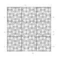
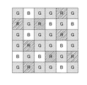
図16は、非特許文献1で開示されているカラーフィルタ配列を示す図である。図17は、ベイヤー配列を示す図である。図16に示すような非周期性の高い(複雑な周期性を有する)カラーフィルタ配列を持つ固体撮像素子から出力された画像信号では、各色の画素の配列が、図17に示すベイヤー配列の固体撮像素子から出力された画像信号と比較して複雑である。
FIG. 16 is a diagram showing a color filter array disclosed in Non-Patent
従って、図16のような6×6画素単位の周期のカラーフィルタ配列を持つ固体撮像素子から出力された画像信号に対して、縮小用の2次元フィルタを用いて縮小処理を実施する際に、以下のような問題点がある。
例えば、1/4の縮小処理を行う際、4×4画素の縮小用の2次元フィルタを用いる。しかしながら、図16に示す固体撮像素子では、カラーフィルタ配列の周期が6×6画素単位であるため、次のような処理を行う。
Therefore, when performing a reduction process using a reduction two-dimensional filter on an image signal output from a solid-state imaging device having a color filter array with a period of 6 × 6 pixels as shown in FIG. There are the following problems.
For example, when a 1/4 reduction process is performed, a two-dimensional filter for reduction of 4 × 4 pixels is used. However, in the solid-state imaging device shown in FIG. 16, the period of the color filter array is 6 × 6 pixels, so the following processing is performed.
図16に示すカラーフィルタの配列を、縦方向と横方向にそれぞれ2面ずつ配置した12×12画素に対して、4×4画素の画素ブロックを9面に分割し、分割した4×4画素の画素ブロックに対し、前記4×4画素の縮小用の2次元フィルタを用いる。しかしながら、前記4×4画素の画素ブロック(前記9面の画素ブロック)のカラーフィルタの並びは全て異なる。このため、カラーフィルタの配列に合わせて、異なるフィルタ係数を持つ縮小用の2次元フィルタが9種類必要となる。 The color filter array shown in FIG. 16 is divided into 4 × 4 pixels by dividing a pixel block of 4 × 4 pixels into 9 planes with respect to 12 × 12 pixels arranged in two planes in the vertical and horizontal directions. The two-dimensional filter for reducing 4 × 4 pixels is used for the pixel block. However, the color filter arrangements of the 4 × 4 pixel block (the nine-surface pixel block) are all different. For this reason, nine kinds of reduction two-dimensional filters having different filter coefficients are required in accordance with the arrangement of the color filters.
一方、図17に示す2×2画素単位の周期のベイヤー配列を持つ固体撮像素子から出力された画像データに対して縮小処理を行う場合には、必要となる4×4画素の縮小用の2次元フィルタは、1種類になる。
以上のように、図16に示す6×6画素単位の周期のカラーフィルタ配列を持つ固体撮像素子では、ベイヤー配列を持つ固体撮像素子と比較して、固体撮像素子から出力された画像信号を縮小処理するために用いる縮小用の2次元のフィルタ係数の数が多くなる。その結果、縮小用の2次元のフィルタ係数を保持するための回路がより多く必要となり、縮小処理回路の規模が大きくなる。
以上のような課題の下、以下に説明する本発明の実施形態に想到した。
On the other hand, when the reduction process is performed on the image data output from the solid-state imaging device having the Bayer arrangement with the cycle of 2 × 2 pixels shown in FIG. 17, the necessary 2 × 4 × 4
As described above, in the solid-state imaging device having the color filter array having the period of 6 × 6 pixels shown in FIG. 16, the image signal output from the solid-state imaging device is reduced as compared with the solid-state imaging device having the Bayer array. The number of reduction two-dimensional filter coefficients used for processing increases. As a result, more circuits for holding the two-dimensional filter coefficients for reduction are required, and the scale of the reduction processing circuit increases.
Under the problems as described above, the present inventors have arrived at an embodiment of the present invention described below.
以下、図面を参照して本発明の一実施形態を説明する。
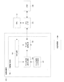
図1は、画像処理装置100の機能的な構成の一例を示す図である。ここでは、画像処理装置100がデジタルカメラである場合を例に挙げて示す。
図1において、結像光学部101は、レンズや絞り等を含み、フォーカス調節や露出調節を行う。
固体撮像素子102は、光学像を電気信号に変換する光電変換機能を有し、CCDやCMOSセンサ等で構成される。本実施形態では、固体撮像素子102に、図16に示す6×6画素単位の周期を持つR、G、Bのカラーフィルタが配置される場合を例に挙げて説明する。各画素から出力される信号レベルは、R、G、B色の何れかに対応した信号レベルとなる。結像光学部101に入射した光は、固体撮像素子102の受光面に結像され、固体撮像素子102からアナログの画像信号として出力される。
Hereinafter, an embodiment of the present invention will be described with reference to the drawings.
FIG. 1 is a diagram illustrating an example of a functional configuration of the
In FIG. 1, an imaging
The solid-
A/D変換部103は、固体撮像素子102から出力されたアナログの画像信号を、図16に示す6×6画素単位のカラーフィルタ配列の並びを持つRAW画像信号(デジタルの画像信号)に変換する。
補正処理部109は、A/D変換部103から出力された画像信号に対して、固体撮像素子102及びA/D変換部103のアナログ特性のばらつき(列アンプの特性ばらつき等)を補正するために、オフセット補正及びゲイン補正を行う。
画像処理部104は、補正処理部109から出力された画像信号に対し、収差補正処理、偽色除去処理、ガンマ処理、補間処理、画像の拡大、縮小といったリサイズ処理等を施す。ここで、補正処理部109の回路から出力される補正処理後の画像信号も、図16に示す6×6画素単位のカラーフィルタ配列の並びを持つRAW画像データである。
The A /
The correction processing unit 109 corrects analog characteristic variations (such as column amplifier characteristic variations) of the solid-
The
メモリインターフェース(I/F)部105は、DRAMで構成されたメモリ106との間で、画像処理部104で処理された画像データや各種制御データの書き込み/読み出しを行う。
CPU107は、画像処理装置100の各種制御を司る。
表示部108は、液晶モニター等で構成される。表示部108は、画像処理部104にて処理された画像データに基づく画像を随時表示し、ユーザがリアルタイムで被写体の様子を観察できるようにする。
A memory interface (I / F)
The
The display unit 108 includes a liquid crystal monitor or the like. The display unit 108 displays an image based on the image data processed by the
ここで、画像処理装置100で行う画像信号の縮小処理の方法の一例を説明する。
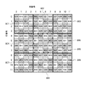
図2は、画像処理装置100で画像信号を1/4に縮小する際の処理対象となる画素ブロックの一例を概念的に示す図である。
図2に示すカラーフィルタの並びは、図16に示す6×6画素単位のカラーフィルタ配列を4面分並べたものとなる。1/4の縮小を行うために、画像処理装置100は、図2に示すように4×4画素単位の画素ブロック201〜209を設定する。
Here, an example of an image signal reduction process performed by the
FIG. 2 is a diagram conceptually illustrating an example of a pixel block to be processed when the
The color filter array shown in FIG. 2 is a color filter array of 6 × 6 pixel units shown in FIG. In order to perform 1/4 reduction, the
画像処理装置100で行う縮小処理では、入力画像信号の4×4画素単位の画素ブロック1つ毎にR、G、Bの各色の画素信号を1つずつ出力する。したがって、R、G、Bの各色で構成される入力画像信号の1/4のサイズのR色の画像信号、G色の画像信号、及びB色の画像信号がそれぞれ出力される。
In the reduction processing performed by the
画像処理装置100は、縮小処理の際に、図16に示す6×6画素単位のカラーフィルタ配列の持つ以下の規則性を利用する。尚、以下の説明では、この規則性を必要に応じて回転規則性と称する。
画素ブロック203を構成するカラーフィルタの並びは、画素ブロック201を構成するカラーフィルタの並びを右方向(時計回り)に90°回転させた並びと一致する。
画素ブロック207を構成するカラーフィルタの並びは、画素ブロック201を構成するカラーフィルタの並びを左方向(反時計回り)に90°回転させた並びと一致する。
画素ブロック209を構成するカラーフィルタの並びは、画素ブロック201を構成するカラーフィルタの並びを180°回転させた並びと一致する。
The
The arrangement of the color filters constituting the
The arrangement of the color filters constituting the
The arrangement of the color filters constituting the pixel block 209 matches the arrangement obtained by rotating the arrangement of the color filters constituting the
画素ブロック204を構成するカラーフィルタの並びは、画素ブロック202を構成するカラーフィルタの並びを左方向に90°回転させた並びと一致する。
画素ブロック206を構成するカラーフィルタの並びは、画素ブロック202を構成するカラーフィルタの並びを右方向に90°回転させた並びと一致する。
画素ブロック208を構成するカラーフィルタの並びは、画素ブロック202を構成するカラーフィルタの並びを180°回転させた並びと一致する。
ただし、画素ブロック205を構成するカラーフィルタの並びは、その他の画素ブロックのカラーフィルタの並びを回転させた並びではない。
The arrangement of the color filters constituting the pixel block 204 matches the arrangement obtained by rotating the arrangement of the color filters constituting the
The arrangement of the color filters constituting the
The arrangement of the color filters constituting the
However, the arrangement of the color filters constituting the
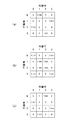
図3は、画素ブロック201の画素値に対して演算処理(縮小処理)する際に使用される各色のフィルタ係数の一例を示す図である。
図3(a)は、図2に示す画素ブロック201の各画素値の一例を示す図である。各画素の位置に示すR0〜R2は、R色の画素値を表し、G0〜G9は、G色の画素値を表し、B0〜B2は、B色の画素値を表す。
図3(b)は、画素ブロック201の縮小処理に用いるR色の画素用のフィルタ係数の一例を示す図である。
FIG. 3 is a diagram illustrating an example of the filter coefficients of the respective colors used when performing arithmetic processing (reduction processing) on the pixel values of the
FIG. 3A is a diagram illustrating an example of each pixel value of the
FIG. 3B is a diagram illustrating an example of a filter coefficient for an R color pixel used for the reduction process of the
図3(c)は、画素ブロック201の縮小処理に用いるG色の画素用のフィルタ係数の一例を示す図である。
図3(d)は、画素ブロック201の縮小処理に用いるB色の画素用のフィルタ係数の一例を示す図である。
尚、各画素の位置が特定しやすいように、図3(a)〜図3(d)において、図の左部に行番号を、図の上部に列番号を表記している。
FIG. 3C is a diagram illustrating an example of the filter coefficient for the G color pixel used for the reduction process of the
FIG. 3D is a diagram illustrating an example of a filter coefficient for a B color pixel used for the reduction process of the
Note that, in order to easily identify the position of each pixel, in FIG. 3A to FIG. 3D, row numbers are shown on the left side of the figure, and column numbers are shown on the top of the figure.
図3(b)〜図3(d)に示すフィルタ係数を用いた計算式は以下の通りになる。画素値R101、G101、B101は、画素ブロック201の16画素が1/4に縮小処理されることにより得られる、R色の画素、G色の画素、B色の画素の1画素分の画素値を表す。
R101=R0*4/17+R1*9/17+R2*4/17
G101=G0*3/46+G1*4/46+G2*3/46+G3*9/46+G4*4/46+G5*9/46+G6*4/46+G7*3/46+G8*4/46+G9*3/46
B101=B0*4/17+B1*4/17+B2*9/17
Calculation formulas using the filter coefficients shown in FIGS. 3B to 3D are as follows. Pixel values R101, G101, and B101 are pixel values for one pixel of an R color pixel, a G color pixel, and a B color pixel obtained by reducing the 16 pixels of the
R101 = R0 * 4/17 + R1 * 9/17 + R2 * 4/17
G101 = G0 * 3/46 + G1 * 4/46 + G2 * 3/46 + G3 * 9/46 + G4 * 4/46 + G5 * 9/46 + G6 * 4/46 + G7 * 3/46 + G8 * 4/46 + G9 * 3/46
B101 = B0 * 4/17 + B1 * 4/17 + B2 * 9/17
次に、図2に示す画素ブロック203の画素値に対して演算処理(縮小処理)する際に使用される各色のフィルタ係数について説明する。
前記回転規則性より、画素ブロック203を構成するカラーフィルタの並びは、画素ブロック201の並びを右方向に90°回転させた並びと一致する。したがって、フィルタ係数も、図3(b)〜図3(d)に示す各色の画素用のフィルタ係数を右方向に90°回転させることにより得られる係数になる。
Next, the filter coefficients of the respective colors used when performing arithmetic processing (reduction processing) on the pixel values of the
Due to the rotation regularity, the arrangement of the color filters constituting the
同様に、図2に示す画素ブロック207の画素値に対して演算処理(縮小処理)する際に使用される各色のフィルタ係数は、図3(b)〜図3(d)に示す各色の画素用のフィルタ係数を左方向に90°回転させることにより得られる係数になる。
同様に、図2に示す画素ブロック209の画素値に対して演算処理(縮小処理)する際に使用される各色のフィルタ係数は、図3(b)〜図3(d)に示す各色の画素用のフィルタ係数を180°回転させることにより得られる係数になる。
Similarly, the filter coefficients of the respective colors used when performing arithmetic processing (reduction processing) on the pixel values of the
Similarly, the filter coefficients of the respective colors used when performing the arithmetic processing (reduction processing) on the pixel values of the
尚、縮小処理後の画素の重心が、画素ブロック201の4×4画素の中心付近になるように、図3(b)〜図3(d)に示す各色の画素用のフィルタ係数の値が設定される。具体的に本実施形態では、図3(b)〜図3(d)に示すように、中心に近い位置にあるフィルタ係数の値の方が、中心から遠い位置にあるフィルタ係数の値よりも大きくなるようにしている。したがって、図3(b)〜図3(d)に示す各色の画素用のフィルタ係数を回転させたフィルタ係数の値も、縮小処理後の画素の重心が各画素ブロック203、207、209の4×4画素の中心付近になるように設定される。この結果、フィルタ係数を回転させたことによる縮小処理後の画素の重心のずれを抑制することが可能である。
Note that the filter coefficient values for the pixels of each color shown in FIGS. 3B to 3D are set so that the center of gravity of the pixel after the reduction processing is near the center of the 4 × 4 pixels of the
図4は、画素ブロック202の画素値に対して演算処理(縮小処理)する際に使用される各色のフィルタ係数の一例を示す図である。
図4(a)は、図2に示す画素ブロック202の各画素値の一例を示す図である。各画素の位置に示すR0〜R3は、R色の画素値を表し、G0〜G7は、G色の画素値を表し、B0〜B3は、B色の画素値を表す。
図4(b)は、画素ブロック202の縮小処理に用いるR色の画素用のフィルタ係数の一例を示す図である。
FIG. 4 is a diagram illustrating an example of the filter coefficients of the respective colors used when performing arithmetic processing (reduction processing) on the pixel values of the
FIG. 4A is a diagram illustrating an example of each pixel value of the
FIG. 4B is a diagram illustrating an example of a filter coefficient for an R color pixel used for the reduction process of the
図4(c)は、画素ブロック202の縮小処理に用いるG色の画素用のフィルタ係数の一例を示す図である。
図4(d)は、画素ブロック202の縮小処理に用いるB色の画素用のフィルタ係数の一例を示す図である。
FIG. 4C is a diagram illustrating an example of the filter coefficient for the G color pixel used for the reduction process of the
FIG. 4D is a diagram illustrating an example of a filter coefficient for a B color pixel used for the reduction process of the
図4(b)〜図4(d)に示すフィルタ係数を用いた計算式は以下の通りになる。画素値R102、G102、B102は、画素ブロック202の16画素が1/4に縮小処理されることにより得られる、R色の画素、G色の画素、B色の画素の1画素分の画素値を表す。
R102=R0*3/19+R1*9/19+R2*4/19+R3*3/19
G102=G0*4/42+G1*4/42+G2*4/42+G3*4/42+G4*9/42+G5*9/42+G6*4/42+G7*4/42
B102=B0*3/19+B1*9/19+B2*4/19+B3*3/19
Calculation formulas using the filter coefficients shown in FIGS. 4B to 4D are as follows. Pixel values R102, G102, and B102 are obtained by reducing the 16 pixels of the
R102 = R0 * 3/19 + R1 * 9/19 + R2 * 4/19 + R3 * 3/19
G102 = G0 * 4/42 + G1 * 4/42 + G2 * 4/42 + G3 * 4/42 + G4 * 9/42 + G5 * 9/42 + G6 * 4/42 + G7 * 4/42
B102 = B0 * 3/19 + B1 * 9/19 + B2 * 4/19 + B3 * 3/19
次に、図2に示す画素ブロック204の画素値に対して演算処理(縮小処理)する際に使用される各色のフィルタ係数について説明する。
前記回転規則性より、画素ブロック204を構成するカラーフィルタの並びは、画素ブロック202の並びを左方向に90°回転させた並びと一致する。したがって、フィルタ係数も、図4(b)〜図4(d)に示す各色の画素用のフィルタ係数を左方向に90°回転させることにより得られる係数になる。
Next, the filter coefficients of the respective colors used when performing arithmetic processing (reduction processing) on the pixel values of the
Due to the rotation regularity, the arrangement of the color filters constituting the
同様に、図2に示す画素ブロック206の画素値に対して演算処理(縮小処理)する際に使用される各色のフィルタ係数は、図4(b)〜図4(d)に示す各色の画素用のフィルタ係数を右方向に90°回転させることにより得られる係数になる。
同様に、図2に示す画素ブロック208の画素値に対して演算処理(縮小処理)する些細に使用される各色のフィルタ係数は、図4(b)〜図4(d)に示す各色の画素用のフィルタ係数を180°回転させることにより得られる係数になる。
Similarly, the filter coefficients of the respective colors used when performing the arithmetic processing (reduction processing) on the pixel values of the
Similarly, the filter coefficients of each color used for performing the calculation process (reduction process) on the pixel values of the
尚、縮小処理後の画素の重心が、画素ブロック202の4×4画素の中心付近になるように、図4(b)〜図4(d)に示す各色の画素用のフィルタ係数の値が設定される。したがって、図4(b)〜図4(d)に示す各色の画素用のフィルタ係数を回転させたフィルタ係数の値も、縮小処理後の画素の重心が各画素ブロック204、206、208の4×4画素の中心付近になるように設定される。この結果、フィルタ係数を回転させたことによる縮小処理後の画素の重心ずれを抑制することが可能である。
It should be noted that the filter coefficient values for the pixels of each color shown in FIGS. 4B to 4D are set so that the center of gravity of the pixel after the reduction process is near the center of the 4 × 4 pixels of the
図5は、画素ブロック205の画素値に対して演算処理(縮小処理)する際に使用される各色のフィルタ係数の一例を示す図である。
図5(a)は、図2に示す画素ブロック205の各画素値の一例を示す図である。各画素の位置を示すR0〜R3は、R色の画素値を表し、G0〜G7は、G色の画素値を表し、B0〜B3は、B色の画素値を表す。
図5(b)は、画素ブロック205の縮小処理に用いるR色の画素用のフィルタ係数の一例を示す図である。
FIG. 5 is a diagram illustrating an example of the filter coefficients of the respective colors used when performing arithmetic processing (reduction processing) on the pixel values of the
FIG. 5A is a diagram illustrating an example of each pixel value of the
FIG. 5B is a diagram illustrating an example of a filter coefficient for an R color pixel used for the reduction process of the
図5(c)は、画素ブロック205の縮小処理に用いるG色の画素用のフィルタ係数の一例を示す図である。
図5(d)は、画素ブロック205の縮小処理に用いるB色の画素用のフィルタ係数の一例を示す図である。
FIG. 5C is a diagram illustrating an example of a filter coefficient for a G pixel used for the reduction process of the
FIG. 5D is a diagram illustrating an example of a filter coefficient for a B color pixel used for the reduction process of the
図5(b)〜図5(d)に示すフィルタ係数を用いた計算式は以下の通りになる。画素値R105、G105、B105は、画素ブロック205の16画素が1/4に縮小処理されることにより得られる、R色の画素、G色の画素、B色の画素の1画素分の画素値を表す。
R105=R0*4/16+R1*4/16+R2*4/16+R3*4/16
G105=G0*3/48+G1*3/48+G2*9/48+G3*9/48+G4*9/48+G5*9/48+G6*3/48+G7*3/48
B105=B0*4/16+B1*4/16+B2*4/16+B3*4/16
Calculation formulas using the filter coefficients shown in FIGS. 5B to 5D are as follows. Pixel values R105, G105, and B105 are obtained by reducing 16 pixels of the
R105 = R0 * 4/16 + R1 * 4/16 + R2 * 4/16 + R3 * 4/16
G105 = G0 * 3/48 + G1 * 3/48 + G2 * 9/48 + G3 * 9/48 + G4 * 9/48 + G5 * 9/48 + G6 * 3/48 + G7 * 3/48
B105 = B0 * 4/16 + B1 * 4/16 + B2 * 4/16 + B3 * 4/16
以上のように、画素ブロック201の画素値に対する演算処理に用いるフィルタ係数を回転させることで、画素ブロック203、207、209の画素値に対する演算処理に用いるフィルタ係数を得ることが可能である。
同様に、画素ブロック202の画素値に対する演算処理に用いるフィルタ係数を回転させることで、画素ブロック204、206、208の画素値に対しする演算処理に用いるフィルタ係数を得ることができる。
As described above, by rotating the filter coefficient used for the calculation process for the pixel value of the
Similarly, by rotating the filter coefficient used for the calculation process for the pixel value of the
したがって、本来であれば縮小処理の際に画素ブロック201〜209用の合計9つのフィルタ係数が必要となる。これに対し、本実施形態では、画素ブロック201、202、205の3つのフィルタ係数で済む。つまり、図16に示す6×6画素単位のカラーフィルタ配列の持つ前記回転規則性を利用することで、縮小処理を行う画像処理装置100に保持するフィルタ係数の数を1/3に削減することが可能である。
Therefore, a total of nine filter coefficients for the pixel blocks 201 to 209 are necessary in the reduction process. On the other hand, in the present embodiment, only three filter coefficients of the pixel blocks 201, 202, and 205 are sufficient. That is, the number of filter coefficients held in the
さらに、1/4の縮小処理を行う方法と同様の考え方で、1/8の縮小処理を行う方法も実現することが可能である。
図6は、画像処理装置100で画像信号を1/8に縮小する際の処理対象となる画素ブロックの一例を概念的に示す図である。
図6に示すカラーフィルタの並びは、図16に示す6×6画素単位のカラーフィルタ配列を縦横4面ずつ合計16面分並べたものとなる。1/8の縮小を行うために、画像処理装置100は、8×8画素単位の画素ブロックを設定する。具体的に画像処理装置100は、左上から順番に8×8画素単位の画素ブロック601〜609を設定する。
Furthermore, a method of performing a 1/8 reduction process can be realized in the same way as a method of performing a 1/4 reduction process.
FIG. 6 is a diagram conceptually illustrating an example of a pixel block to be processed when the
The arrangement of the color filters shown in FIG. 6 is a color filter array of 6 × 6 pixels shown in FIG. In order to perform 1/8 reduction, the
画像処理装置100で行う縮小処理では、入力画像信号の8×8画素単位の画素ブロック1つ毎にR、G、Bの各色の画素信号を1つずつ出力する。したがって、R、G、Bの各色で構成される入力画像信号の1/8のサイズのR色の画像信号、G色の画像信号、及びB色の画像信号がそれぞれ出力される。
In the reduction processing performed by the
画像処理装置100は、縮小処理の際に、図16に示す6×6画素単位のカラーフィルタ配列の持つ以下の規則性を利用する。尚、以下の説明では、この規則性も必要に応じて回転規則性と称する。
画素ブロック603を構成するカラーフィルタの並びは、画素ブロック601を構成するカラーフィルタの並びを右方向に90°回転させた並びと一致する。
画素ブロック607を構成するカラーフィルタの並びは、画素ブロック601を構成するカラーフィルタの並びを左方向に90°回転させた並びと一致する。
画素ブロック609を構成するカラーフィルタの並びは、画素ブロック601を構成するカラーフィルタの並びを180°回転させた並びと一致する。
The
The arrangement of the color filters constituting the pixel block 603 coincides with the arrangement obtained by rotating the arrangement of the color filters constituting the pixel block 601 90 ° to the right.
The arrangement of the color filters constituting the pixel block 607 matches the arrangement obtained by rotating the arrangement of the color filters constituting the pixel block 601 90 ° to the left.
The arrangement of the color filters constituting the pixel block 609 matches the arrangement obtained by rotating the arrangement of the color filters constituting the pixel block 601 by 180 °.
画素ブロック604を構成するカラーフィルタの並びは、画素ブロック602を構成するカラーフィルタの並びを左方向に90°回転させた並びと一致する。
画素ブロック606を構成するカラーフィルタの並びは、画素ブロック602を構成するカラーフィルタの並びを右方向に90°回転させた並びと一致する。
画素ブロック608を構成するカラーフィルタの並びは、画素ブロック602を構成するカラーフィルタの並びを180°回転させた並びと一致する。
ただし、画素ブロック605を構成するカラーフィルタの並びは、その他の画素ブロックのカラーフィルタの並びを回転させた並びではない。
The arrangement of the color filters constituting the pixel block 604 matches the arrangement obtained by rotating the arrangement of the color filters constituting the pixel block 602 90 degrees to the left.
The arrangement of the color filters constituting the pixel block 606 matches the arrangement obtained by rotating the arrangement of the color filters constituting the pixel block 602 90 degrees to the right.
The arrangement of the color filters constituting the pixel block 608 matches the arrangement obtained by rotating the arrangement of the color filters constituting the pixel block 602 by 180 °.
However, the arrangement of the color filters constituting the pixel block 605 is not an arrangement obtained by rotating the arrangement of the color filters of the other pixel blocks.
前述した1/4の縮小処理の方法と同様の考え方を用いて、縮小処理の際に画素ブロック601の画素値に対する演算処理に用いるフィルタ係数を回転させることで画素ブロック603、607、609の画素値に対して用いるフィルタ係数を得ることができる。
同様に、画素ブロック602の画素値に対する演算処理に用いるフィルタ係数を回転させることで画素ブロック604、606、608の画素値に対する演算処理に用いるフィルタ係数を得ることができる。
Using the same idea as the 1/4 reduction processing method described above, the pixels of the pixel blocks 603, 607, and 609 are rotated by rotating the filter coefficient used for the calculation processing on the pixel value of the pixel block 601 during the reduction processing. The filter coefficient used for the value can be obtained.
Similarly, by rotating the filter coefficient used for the calculation process for the pixel value of the pixel block 602, the filter coefficient used for the calculation process for the pixel value of the pixel blocks 604, 606, and 608 can be obtained.
したがって、本来であれば縮小処理の際に画素ブロック601〜609用の合計9つのフィルタ係数が必要となる。これに対し、本実施形態では、画素ブロック601、602、605の3つのフィルタ係数で済む。つまり、前述した1/4の縮小処理と同様に1/8の縮小処理においても、図16に示す6×6画素単位のカラーフィルタ配列の持つ前記回転規則性を利用することで、縮小処理を行う画像処理装置100に保持するフィルタ係数の数を1/3に削減が可能である。
Therefore, a total of nine filter coefficients for the pixel blocks 601 to 609 are necessary in the reduction process. In contrast, in this embodiment, only three filter coefficients of the pixel blocks 601, 602, and 605 are sufficient. That is, in the reduction processing of 1/8 as well as the reduction processing of 1/4 described above, the reduction processing is performed by using the rotation regularity of the color filter array of 6 × 6 pixels shown in FIG. The number of filter coefficients held in the
さらに1/8の縮小処理では、画素ブロックが8×8画素単位である(図6を参照)。このため、1画素ブロック当たりのフィルタ係数も64(=8×8)個となる。したがって、1/4の縮小処理よりも、1/8の縮小処理の方が、フィルタ係数の数の削減効果は大きい。
また、或る画素ブロックの画素値に対して用いるフィルタ係数を回転することにより、別の画素ブロックの画素値に対して用いるフィルタ係数を得る方法は、その他の縮小倍率にも適応することが可能である。このため、以下に、前述した1/4の縮小処理及び1/8の縮小処理を含め、縮小処理が可能なカラーフィルタの周期性と画像データの縮小倍率について、一般的な表現を記述する。
Further, in the 1/8 reduction process, the pixel block is 8 × 8 pixel units (see FIG. 6). For this reason, the number of filter coefficients per pixel block is 64 (= 8 × 8). Therefore, the 1/8 reduction process has a greater effect of reducing the number of filter coefficients than the 1/4 reduction process.
In addition, the method of obtaining the filter coefficient used for the pixel value of another pixel block by rotating the filter coefficient used for the pixel value of a certain pixel block can be applied to other reduction ratios. It is. Therefore, in the following, general expressions will be described regarding the periodicity of the color filter that can be reduced and the reduction rate of the image data, including the 1/4 reduction process and the 1/8 reduction process described above.
本実施形態に係る画像処理装置100の備える固体撮像素子102は、基本となるカラーフィルタの並びについて画素ブロックの中心の画素に関して点対称性を持つN×N画素の画素ブロックを持つ(N:正の整数)。また、固体撮像素子102のカラーフィルタは、前記N×N画素の画素ブロックを90°回転した画素ブロックを縦方向(垂直方向)と横方向(水平方向)の各々で交互に配置することにより、2N×2N画素単位の周期の色の配列を有する。
The solid-
以上のようなカラーフィルタ配列を持つ固体撮像素子102から出力された画像信号に対して、以下の縮小処理が可能である。
M×M画素単位の画素ブロックに対して、前記回転規則性を利用して、縮小用のM×Mのフィルタ係数を回転させて演算処理することで、少ないフィルタ係数で1/Mの縮小処理が実現可能である(M:1以外の正の整数かつ2Nの正の整数倍Kの約数)。
1/4の縮小処理では、N=3、M=4、K=12となり、1/8の縮小処理では、N=3、M=8、K=24となる。
その他、1/2の縮小処理では、N=3、M=2、K=6となり、1/3の縮小処理では、N=3、M=3、K=6となり、1/6の縮小処理では、N=3、M=6、K=12となる。また、1/9の縮小処理では、N=3、M=9、K=18となり、1/12の縮小処理では、N=3、M=12、K=24となる。
The following reduction processing can be performed on the image signal output from the solid-
By reducing the M × M filter coefficient for reduction using the rotation regularity and performing arithmetic processing on the pixel block in units of M × M pixels, 1 / M reduction processing is performed with a small number of filter coefficients. (M is a positive integer other than 1 and a divisor of a positive integer multiple K of 2N).
In the 1/4 reduction process, N = 3, M = 4, and K = 12, and in the 1/8 reduction process, N = 3, M = 8, and K = 24.
In addition, in the 1/2 reduction processing, N = 3, M = 2, and K = 6, and in the 1/3 reduction processing, N = 3, M = 3, and K = 6, and 1/6 reduction processing. Then, N = 3, M = 6, and K = 12. In the 1/9 reduction process, N = 3, M = 9, and K = 18, and in the 1/12 reduction process, N = 3, M = 12, and K = 24.
以下、1/4の縮小処理を実施するための画像処理装置100の構成並びにその制御方法の一例を説明する。
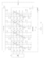
図7は、図1に示す画像処理部104に具備される画像縮小回路701の機能的な構成の一例を示す図である。
図7において、画像縮小回路701は、補正処理部109から入力された、図16に示す6×6画素単位のカラーフィルタ配列の並びを持ったRAW画像信号の縮小処理を実施する回路である。
Hereinafter, an example of the configuration of the
FIG. 7 is a diagram illustrating an example of a functional configuration of the
In FIG. 7, an
制御回路705は、各種信号を出力して画像縮小回路701内の各機能ブロックの制御を行うための回路である。
フィルタ係数レジスタ回路702は、前記RAW画像信号の画素ブロックに対して演算処理を行う縮小処理用のフィルタ係数を設定するレジスタ回路である。
フィルタ係数読出し回路703は、フィルタ係数レジスタ回路702に設定された前記縮小処理用のフィルタ係数を、制御回路705から出力される制御信号により指定された順番で読み出すための回路である。
フィルタ演算回路704は、補正処理部109から入力した前記RAW画像信号に対して、フィルタ係数読出し回路703から入力したフィルタ係数を演算処理するための回路である。
The
The filter
The filter
The
図8は、前記RAW画像信号の一部分の画素値の一例を示す図である。図8の各色の画素値の並びは、図2に示すカラーフィルタ配列の並び方に準じている。図8中のR※の記号はR色の画素値を、G※の記号はG色の画素値を、B※の記号はB色の画素値を各々示す。ただし、※は数字を表す。尚、各画素の位置が特定しやすいように、図8において、図の左部に行番号を、図の上部に列番号を表記する。 FIG. 8 is a diagram showing an example of a pixel value of a part of the RAW image signal. The arrangement of the pixel values of each color in FIG. 8 conforms to the arrangement of the color filter array shown in FIG. In FIG. 8, the symbol R * indicates an R color pixel value, the symbol G * indicates a G pixel value, and the symbol B * indicates a B pixel value. However, * represents a number. In FIG. 8, the row number is shown on the left side of the figure and the column number is shown on the upper part of the figure so that the position of each pixel can be easily identified.
フィルタ演算回路704には、図8に示す前記RAW画像信号の行番号0〜3の左側の画素(図8の画素値G10、R10、G14、G17の画素)から、4画素ずつ画素値が順次入力される。その後は、入力する画素が右方向に一列ずつ移動し、図8に示す前記RAW画像信号の右端部まで処理が達した後は、次の行(図8に示す行番号4〜7)の左側の画素(画素値B40、G41、G40、R40の画素)から、4画素ずつ画素値が順次入力される。以後、全ての前記RAW画像信号の画素値が入力されるまで処理が続く。
In the filter
また、図16に示す6×6画素単位のカラーフィルタ配列の持つ前記回転規則性より、図8中の画素ブロック803の画素の色の並びは、画素ブロック801の画素の色の並びを右方向に90°回転した並びになる。
同じく画素ブロック807の画素の色の並びは、画素ブロック801の並びを左方向に90°回転した並びとなり、画素ブロック809の画素の色の並びは画素ブロック801の並びを180°回転した並びになる。
さらに画素ブロック804の色の並びは、画素ブロック802の並びを左方向に90°回転した並びとなり、画素ブロック806の並びは画素ブロック802を右方向に90°回転した並びになる。画素ブロック808の並びは画素ブロック802を180°回転した並びになる。
Further, due to the rotation regularity of the 6 × 6 pixel unit color filter array shown in FIG. 16, the pixel color arrangement of the
Similarly, the arrangement of the pixel colors of the pixel block 807 is an arrangement obtained by rotating the arrangement of the pixel blocks 801 by 90 ° to the left, and the arrangement of the pixel colors of the
Further, the color arrangement of the pixel block 804 is an arrangement obtained by rotating the arrangement of the
次に、フィルタ係数レジスタ回路702の構成について説明する。
フィルタ係数レジスタ回路702は、4×4画素分の2次元のフィルタ係数を設定するフィルタレジスタを持つ。後述するフィルタ演算回路704は、各画素ブロックで、R、G、Bの各色の画素値に対してフィルタ係数を積算する。このため、フィルタ係数レジスタ回路702は、一つの画素ブロック当たり、R色画素用フィルタレジスタ、G色画素用フィルタレジスタ、及びB色画素用フィルタレジスタの合計3つ前記フィルタレジスタを持つ。
Next, the configuration of the filter
The filter
図9は、フィルタ係数レジスタ回路702が有する各色の前記フィルタレジスタに設定される画素ブロック801用のフィルタ係数の一例を示す図である。
図9中のF_R1※、F_G1※、F_B1※は、各フィルタレジスタに設定されるフィルタ係数を示す。ただし、※は数字を表わす。尚、画素ブロック801内にフィルタ係数の処理対象となる色の画素が存在しない場合は、図9に示すように、該当するフィルタレジスタに0(ゼロ)が設定される。
FIG. 9 is a diagram illustrating an example of filter coefficients for the
F_R1 *, F_G1 *, and F_B1 * in FIG. 9 indicate filter coefficients set in each filter register. However, * represents a number. If there is no color pixel to be processed by the filter coefficient in the
図9(a)は、画素ブロック801の縮小処理に用いる前記R色画素用フィルタレジスタに設定されるフィルタ係数の一例を示す図である。
画素ブロック801のR色の画素に対しては、前述したように図3(b)に示すフィルタ係数を設定する。したがって、図9(a)において、フィルタ係数F_R10、F_R12として4/17が、フィルタ係数F_R11として9/17がそれぞれ設定される(F_R10=F_R12=4/17、F_R11=9/17)。
FIG. 9A is a diagram illustrating an example of filter coefficients set in the R color pixel filter register used for the reduction process of the
As described above, the filter coefficient shown in FIG. 3B is set for the R color pixel of the
図9(b)は、画素ブロック801の縮小処理に用いる前記G色画素用フィルタレジスタに設定されるフィルタ係数の一例を示す図である。
画素ブロック801のG色の画素に対しては、前述したように図3(c)に示すフィルタ係数を設定する。したがって、図9(b)において、フィルタ係数F_G10、F_G12、F_G17、F_G19として3/46が設定される(F_G10=F_G12=F_G17=F_G19=3/46)。また、フィルタ係数F_G11、F_G14、F_G16、F_G18として4/46が設定される(F_G11=F_G14=F_G16=F_G18=4/46)。また、フィルタ係数F_G13、F_G15として9/46が設定される(F_G13=F_G15=9/46)。
FIG. 9B is a diagram illustrating an example of filter coefficients set in the G color pixel filter register used for the reduction processing of the
As described above, the filter coefficient shown in FIG. 3C is set for the G color pixel of the
図9(c)は、画素ブロック801の縮小処理に用いる前記B色画素用フィルタレジスタに設定されるフィルタ係数の一例を示す図である。
画素ブロック801のB色の画素に対しては、前述したように図3(d)に示すフィルタ係数を設定する。したがって、図9(c)において、フィルタ係数F_B10、F_B11として4/17が、フィルタ係数F_B12として9/17がそれぞれ設定される(F_B10=F_B11=4/17、F_B12=9/17)。
FIG. 9C is a diagram illustrating an example of filter coefficients set in the B color pixel filter register used for the reduction process of the
As described above, the filter coefficient shown in FIG. 3D is set for the B color pixel of the
同様に図10は、フィルタ係数レジスタ回路702が有する各色の前記フィルタレジスタに設定される画素ブロック802用のフィルタ係数の一例を示す図である。
図10中のF_R2※、F_G2※、F_B2※は、各フィルタレジスタに設定されるフィルタ係数を示す。ただし、※は数字を表わす。尚、画素ブロック802内にフィルタ係数の処理対象となる色の画素が存在しない場合は、図10に示すように、該当するフィルタレジスタに0(ゼロ)を設定する。
Similarly, FIG. 10 is a diagram illustrating an example of filter coefficients for the
F_R2 *, F_G2 *, and F_B2 * in FIG. 10 indicate filter coefficients set in each filter register. However, * represents a number. If there is no color pixel to be processed by the filter coefficient in the
図10(a)は、画素ブロック802の縮小処理に用いる前記R色画素用フィルタレジスタに設定されるフィルタ係数の一例を示す図である。
画素ブロック802のR色の画素に対しては、前述したように図4(b)に示すフィルタ係数を設定する。したがって、図10(a)において、フィルタ係数F_R20、F_R23として3/19が設定される(F_R20=F_R23=3/19)。また、フィルタ係数F_R21として9/19が、フィルタ係数F_R22として4/19がそれぞれ設定される(F_R21=9/19、F_R22=4/19)。
FIG. 10A is a diagram illustrating an example of filter coefficients set in the R color pixel filter register used for the reduction process of the
As described above, the filter coefficient shown in FIG. 4B is set for the R color pixel of the
図10(b)は、画素ブロック802の縮小処理に用いる前記G色画素用フィルタレジスタに設定されるフィルタ係数の一例を示す図である。
画素ブロック802のG色の画素に対しては、前述したように図4(c)に示すフィルタ係数を設定する。したがって、図10(b)において、フィルタ係数F_G20、F_G21、F_G22、F_G23、F_G26、F_G27として4/42が設定される(F_G20=F_G21=F_G22=F_G23=F_G26=F_G27=4/42)。また、フィルタ係数F_G24、F_G25として9/42が設定される(F_G24=F_G25=9/42)。
FIG. 10B is a diagram illustrating an example of filter coefficients set in the G color pixel filter register used for the reduction process of the
As described above, the filter coefficient shown in FIG. 4C is set for the G color pixel of the
図10(c)は、画素ブロック802の縮小処理に用いる前記B色画素用フィルタレジスタに設定されるフィルタ係数の一例を示す図である。
画素ブロック802のB色の画素に対しては、前述したように図4(d)に示すフィルタ係数を設定する。したがって、図10(c)において、フィルタ係数F_B20、F_B23として3/19が設定される(F_B20=F_B23=3/19)。また、フィルタ係数F_B21として9/19が、フィルタ係数F_B22として4/19がそれぞれ設定される(F_B21=9/19、F_B22=4/19)。
FIG. 10C is a diagram illustrating an example of filter coefficients set in the B color pixel filter register used for the reduction process of the
As described above, the filter coefficient shown in FIG. 4D is set for the B color pixel of the
同様に図11は、フィルタ係数レジスタ回路702が有する各色の前記フィルタレジスタに設定される画素ブロック805用のフィルタ係数の一例を示す図である。
図11中のF_R3※、F_G3※、F_B3※は、各フィルタレジスタに設定されるフィルタ係数を示す。ただし、※は数字を表わす。尚、画素ブロック805内にフィルタ係数の処理対象となる色の画素が存在しない場合は、図11に示すように、該当するフィルタレジスタに0(ゼロ)を設定する。
Similarly, FIG. 11 is a diagram illustrating an example of filter coefficients for the
F_R3 *, F_G3 *, and F_B3 * in FIG. 11 indicate filter coefficients set in each filter register. However, * represents a number. If there is no color pixel to be processed by the filter coefficient in the
図11(a)は、画素ブロック805の縮小処理に用いる前記R色画素用フィルタレジスタに設定されるフィルタ係数の一例を示す図である。
画素ブロック805のR色の画素に対しては、前述したように図5(b)に示すフィルタ係数を設定する。したがって、図11(a)において、フィルタ係数F_B30、F_B31、F_B32、F_B33として4/16が設定される(F_B30=F_B31=F_B32=F_B33=4/16)。
FIG. 11A is a diagram illustrating an example of filter coefficients set in the R color pixel filter register used for the reduction process of the
As described above, the filter coefficient shown in FIG. 5B is set for the R color pixel of the
図11(b)は、画素ブロック805の縮小処理に用いる前記G色画素用フィルタレジスタに設定されるフィルタ係数の一例を示す図である。
画素ブロック805のG色の画素に対しては、前述したように図5(c)に示すフィルタ係数を設定する。したがって、図11(b)において、フィルタ係数F_G30、F_G31、F_G36、F_G37として3/48が設定される(F_G30=F_G31=F_G36=F_G37=3/48)。また、フィルタ係数F_G32、F_G33、F_G34、F_G35として9/48が設定される(F_G32=F_G33=F_G34=F_G35=9/48)。
FIG. 11B is a diagram illustrating an example of filter coefficients set in the G color pixel filter register used for the reduction process of the
As described above, the filter coefficient shown in FIG. 5C is set for the G color pixel in the
図11(c)は、画素ブロック805の縮小処理に用いる前記B色画素用フィルタレジスタに設定されるフィルタ係数の一例を示す図である。
画素ブロック805のB色の画素に対しては、前述したように図4(d)に示すフィルタ係数を設定する。したがって、図11(c)において、フィルタ係数F_R30、F_R31、F_R32、F_R33として4/16が設定される(F_R30=F_R31=F_R32=F_R33=4/16)。
尚、各フィルタレジスタの位置及びフィルタ係数が特定しやすいように、図9〜図11の各図において、図の左部に行番号を、図の上部に列番号を表記している。以下の説明では、前記行番号、列番号を参照する。
FIG. 11C is a diagram illustrating an example of filter coefficients set in the B color pixel filter register used for the reduction process of the
As described above, the filter coefficient shown in FIG. 4D is set for the B color pixel in the
In order to make it easy to specify the position and filter coefficient of each filter register, in each of FIGS. 9 to 11, the row number is shown on the left side of the figure and the column number is shown on the top of the figure. In the following description, the row number and the column number are referred to.
図12は、フィルタ演算回路704の内部構成の一例を示す図である。尚、フィルタ演算回路704内の各回路は、フィルタ演算回路704に入力されるCLK信号(不図示)の立ち上がりに同期して1サイクル毎に処理を行う。
図12において、フィルタ演算回路704は、画素値加算回路1206と、積算回路1200〜1203、1210〜1213、1220〜1223、1230〜1233と、フリップフロップ回路1250〜1261と、を有する。
画素値加算回路1206は、制御回路705の制御により、演算処理後の画素値の加算処理を行う。
FIG. 12 is a diagram illustrating an example of the internal configuration of the filter
In FIG. 12, the filter
The pixel value addition circuit 1206 performs addition processing of the pixel values after the arithmetic processing under the control of the
ここで、図12に示す各信号sigについて説明する。
まず、信号sig400、sig500は夫々、制御回路705からフィルタ係数読出し回路703、画素値加算回路1206へ処理のタイミングや処理内容を伝達させるための信号である。
尚、制御回路705は、画像縮小回路701に入力される画素数をカウントする。制御回路705は、このカウントした画素数に基づいて、処理対象の画素が、何処の画素ブロックに属しているかを判定する。制御回路705は、この判定結果を、画素ブロック指定制御信号(図12中の信号sig400)として、フィルタ係数読み出し回路703に出力する。
フィルタ係数読み出し回路703は、入力した前記画素ブロック指定制御信号(信号sig400)に示されている画素ブロックのR色画素用フィルタレジスタ、G色画素用フィルタレジスタ、B色画素用フィルタレジスタから順次フィルタ係数を読み出す。
Here, each signal sig shown in FIG. 12 will be described.
First, signals sig400 and sig500 are signals for transmitting processing timing and processing contents from the
Note that the
The filter
画像データ入力信号であるDATA_IN03信号、DATA_IN13信号、DATA_IN23信号、DATA_IN33信号(各々図12中の信号sig103、113、123、133)には、以下の信号が入力される。すなわち、補正処理部109から前記RAW画像信号が4画素ずつ順次入力される。
図8に示す例を用いて具体的に説明を行うと、DATA_IN03信号(信号sig103)には、図8の行番号0、4、8の画素値が、図8の左側から順次入力される。また、DATA_IN13信号(信号sig113)には、図8の行番号1、5、9の画素値が、図8の左側から順次入力される。DATA_IN23信号(信号sig123)には、図8の行番号2、6、10の画素値が、DATA_IN33信号(信号sig133)には、図8の行番号3、7、11の画素値が、それぞれ図8の左側から順次入力される。
The following signals are input to the DATA_IN03 signal, DATA_IN13 signal, DATA_IN23 signal, and DATA_IN33 signal (signals sig103, 113, 123, and 133 in FIG. 12, respectively) that are image data input signals. That is, the RAW image signal is sequentially input from the correction processing unit 109 every four pixels.
Specifically, the pixel values of
入力された画像データ入力信号は、各フリップフロップ回路1250〜1208により、CLK信号の立ち上がりに同期して以下の通り伝搬される。
DATA_IN03信号(信号sig103)は、フリップフロップ回路1250により、DATA_IN02信号(信号sig102)として出力される。次のCLK信号の立ち上がりに同期して、DATA_IN02信号(信号sig102)は、フリップフロップ回路1251により、DATA_IN01信号(信号sig101)として出力される。さらにその次のCLK信号の立ち上がりに同期して、DATA_IN01信号(信号sig101)は、フリップフロップ回路1252により、DATA_IN00信号(信号sig100)として出力される。
The input image data input signal is propagated by the flip-flop circuits 1250 to 1208 as follows in synchronization with the rising edge of the CLK signal.
The DATA_IN03 signal (signal sig103) is output as a DATA_IN02 signal (signal sig102) by the flip-flop circuit 1250. In synchronization with the next rising edge of the CLK signal, the DATA_IN02 signal (signal sig102) is output as a DATA_IN01 signal (signal sig101) by the flip-flop circuit 1251. Further, in synchronization with the next rising edge of the CLK signal, the DATA_IN01 signal (signal sig101) is output as the DATA_IN00 signal (signal sig100) by the flip-flop circuit 1252.
DATA_IN13信号(信号sig113)は、フリップフロップ回路1253により、DATA_IN12信号(信号sig112)として出力される。次のCLK信号の立ち上がりに同期して、DATA_IN12信号(信号sig112)は、フリップフロップ回路1254により、DATA_IN11信号(信号sig111)として出力される。さらに次のCLK信号の立ち上がりに同期して、DATA_IN11信号(信号sig111)は、フリップフロップ回路1255により、DATA_IN10信号(信号sig110)として出力される。 The DATA_IN13 signal (signal sig113) is output as a DATA_IN12 signal (signal sig112) by the flip-flop circuit 1253. In synchronization with the next rising edge of the CLK signal, the DATA_IN12 signal (signal sig112) is output as the DATA_IN11 signal (signal sig111) by the flip-flop circuit 1254. Further, in synchronization with the next rising edge of the CLK signal, the DATA_IN11 signal (signal sig111) is output as a DATA_IN10 signal (signal sig110) by the flip-flop circuit 1255.
DATA_IN23信号(信号sig123)は、フリップフロップ回路1256により、DATA_IN22信号(信号sig122)として出力される。次のCLK信号の立ち上がりに同期して、DATA_IN22信号(信号sig122)は、フリップフロップ回路1257により、DATA_IN21信号(信号sig121)として出力される。さらに次のCLK信号の立ち上がりに同期して、DATA_IN21信号(信号sig121)は、フリップフロップ回路1258により、DATA_IN20信号(信号sig120)として出力される。 The DATA_IN23 signal (signal sig123) is output as a DATA_IN22 signal (signal sig122) by the flip-flop circuit 1256. In synchronization with the next rise of the CLK signal, the DATA_IN22 signal (signal sig122) is output as a DATA_IN21 signal (signal sig121) by the flip-flop circuit 1257. Further, in synchronization with the next rising edge of the CLK signal, the DATA_IN21 signal (signal sig121) is output as a DATA_IN20 signal (signal sig120) by the flip-flop circuit 1258.
DATA_IN33信号(信号sig133)は、フリップフロップ回路1259により、DATA_IN32信号(信号sig132)として出力される。次のCLK信号の立ち上がりに同期して、DATA_IN32信号(信号sig132)は、フリップフロップ回路1260により、DATA_IN31信号(信号sig131)として出力される。さらにその次のCLK信号の立ち上がりに同期して、DATA_IN31信号(信号sig131)は、フリップフロップ回路1261により、DATA_IN30信号(信号sig130)として出力される。
The DATA_IN33 signal (signal sig133) is output as a DATA_IN32 signal (signal sig132) by the flip-flop circuit 1259. In synchronization with the next rising edge of the CLK signal, the DATA_IN32 signal (signal sig132) is output as the DATA_IN31 signal (signal sig131) by the flip-flop circuit 1260. Further, in synchronization with the next rising edge of the CLK signal, the DATA_IN31 signal (signal sig131) is output as a DATA_IN30 signal (signal sig130) by the flip-
フィルタ係数信号FIL00〜FIL04(各々図12中の信号sig00〜sig04)には、フィルタ係数読み出し回路703から読み出されたフィルタ係数が入力される。
フィルタ係数信号FIL10〜FIL14(信号sig10〜sig14)、FIL20〜FIL24(信号sig20〜sig24)、FIL30〜FIL34(信号sig30〜sig34)にも、同様にフィルタ係数が入力される。
The filter coefficients read from the filter
Filter coefficients are similarly input to the filter coefficient signals FIL10 to FIL14 (signals sig10 to sig14), FIL20 to FIL24 (signals sig20 to sig24), and FIL30 to FIL34 (signals sig30 to sig34).
積算回路1200は、フィルタ係数信号FIL00(信号sig00)と、DATA_IN00信号(信号sig100)とを積算し、その結果を、MULT_OUT00信号(信号sig200)として出力する。
積算回路1201は、フィルタ係数信号FIL01(信号sig01)と、DATA_IN01信号(信号sig101)とを積算し、その結果を、MULT_OUT01信号(信号sig201)として出力する。
The integrating circuit 1200 integrates the filter coefficient signal FIL00 (signal sig00) and the DATA_IN00 signal (signal sig100), and outputs the result as a MULT_OUT00 signal (signal sig200).
The integrating circuit 1201 integrates the filter coefficient signal FIL01 (signal sig01) and the DATA_IN01 signal (signal sig101), and outputs the result as a MULT_OUT01 signal (signal sig201).
積算回路1202は、フィルタ係数信号FIL02信号(信号sig02)と、DATA_IN00信号(信号sig102)とを積算し、その結果を、MULT_OUT02信号(信号sig202)として出力する。
積算回路1203は、フィルタ係数信号FIL03(信号sig03)と、DATA_IN03信号(信号sig103)とを積算し、その結果を、MULT_OUT03信号(信号sig203)として出力する。
The integrating circuit 1202 integrates the filter coefficient signal FIL02 signal (signal sig02) and the DATA_IN00 signal (signal sig102), and outputs the result as a MULT_OUT02 signal (signal sig202).
The integrating circuit 1203 integrates the filter coefficient signal FIL03 (signal sig03) and the DATA_IN03 signal (signal sig103), and outputs the result as a MULT_OUT03 signal (signal sig203).
同様に、積算回路1210〜1213の各々で、フィルタ係数信号FIL10〜FIL13(信号sig10〜sig13)と、DATA_IN10〜DATA_IN13信号(信号sig110〜sig113)との積算処理が実施される。積算の結果は、各々MULT_OUT10〜MULT_OUT13信号(信号sig210〜sig213)として出力される。
同様に、積算回路1220〜1223の各々で、フィルタ係数信号FIL20〜FIL23(信号sig20〜sig23)と、DATA_IN20〜DATA_IN23信号(信号sig120〜sig123)との積算処理が実施される。積算の結果は、各々MULT_OUT20〜MULT_OUT23信号(信号sig220〜sig223)として出力される。
Similarly, the integration processes of the filter coefficient signals FIL10 to FIL13 (signals sig10 to sig13) and the DATA_IN10 to DATA_IN13 signals (signals sig110 to sig113) are performed in each of the integration circuits 1210 to 1213. The result of integration is output as MULTI_OUT10 to MULTI_OUT13 signals (signals sig210 to sig213), respectively.
Similarly, integration processing of filter coefficient signals FIL20 to FIL23 (signal sig20 to sig23) and DATA_IN20 to DATA_IN23 signals (signal sig120 to sig123) is performed in each of the integration circuits 1220 to 1223. The results of integration are output as MULT_OUT20 to MULT_OUT23 signals (signals sig220 to sig223), respectively.
同様に、積算回路1230〜1233の各々で、フィルタ係数信号FIL30〜FIL33(信号sig30〜sig33)と、DATA_IN30〜DATA_IN33信号(信号sig130〜sig133)との積算処理が実施される。積算の結果は、各々MULT_OUT30〜MULT_OUT33信号(信号sig230〜sig233)として出力される。 Similarly, integration processing of filter coefficient signals FIL30 to FIL33 (signal sig30 to sig33) and DATA_IN30 to DATA_IN33 signals (signal sig130 to sig133) is performed in each of the integration circuits 1230 to 1233. The results of integration are output as MULT_OUT30 to MULT_OUT33 signals (signals sig230 to sig233), respectively.
画素値加算回路1206は、以下の合計16の信号の加算処理を実施する。この信号として、第1に、MULT_OUT00〜MULT_OUT03信号(信号sig200〜203)の4つの信号がある。第2に、MULT_OUT10〜MULT_OUT13信号(信号sig210〜213)の4つの信号がある。第3に、MULT_OUT20〜MULT_OUT23信号(信号sig220〜223)の4つの信号がある。第4に、MULT_OUT30〜MULT_OUT33信号(信号sig230〜233)の4つの信号がある。加算の結果は、画像データ出力信号DATA_OUT(信号sig300)としてメモリI/F部105に出力される。
The pixel value addition circuit 1206 performs the following addition processing of a total of 16 signals. As this signal, first, there are four signals of MULTI_OUT00 to MULTI_OUT03 signals (signals sig200 to 203). Second, there are four signals, MULTI_OUT10 to MULTI_OUT13 signals (signals sig210 to 213). Thirdly, there are four signals, MULT_OUT20 to MULT_OUT23 signals (signals sig220 to 223). Fourthly, there are four signals, MULT_OUT30 to MULT_OUT33 signals (signals sig230 to 233). The result of addition is output to the memory I /
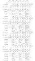
図13〜図15は、図8に示すRAW画像データの縮小処理を行う際のフィルタ演算回路704の各種信号のタイミングチャートの一例を示す図である。
図13は、図8に示す画素ブロック801〜803を縮小処理する期間におけるフィルタ演算回路704の各種信号のタイミングチャートの一例を示す図である。
以下、図13を用いて、画素ブロック801〜803を縮小処理する際のフィルタ演算回路704による制御方法を説明する。
図13に示す期間A−1において、DATA_IN03信号(信号sig103)に入力された図8に示す行番号0の画素信号が、フリップフロップ回路1250〜1252により、次のように順次伝搬される。
DATA_IN02信号(信号sig102)→DATA_IN01信号(信号sig101)→DATA_IN00信号(信号sig100)。
13 to 15 are diagrams illustrating examples of timing charts of various signals of the filter
FIG. 13 is a diagram illustrating an example of a timing chart of various signals of the filter
Hereinafter, a control method by the filter
In the period A-1 illustrated in FIG. 13, the pixel signal of
DATA_IN02 signal (signal sig102) → DATA_IN01 signal (signal sig101) → DATA_IN00 signal (signal sig100).
同期間A−1おいて同様に、DATA_IN13信号(信号sig113)に入力された図8に示す行番号1の画素信号が、フリップフロップ回路1253〜1255により、次のように順次伝搬される。
DATA_IN12信号(信号sig112)→DATA_IN11信号(信号sig111)→DATA_IN10信号(信号sig110)。
Similarly, in the same period A-1, the pixel signal of
DATA_IN12 signal (signal sig112) → DATA_IN11 signal (signal sig111) → DATA_IN10 signal (signal sig110).
同期間A−1おいて同様に、DATA_IN23信号(信号sig123)に入力された図8に示す行番号2の画素信号が、フリップフロップ回路1256〜1258により、次のように順次伝搬される。
DATA_IN22信号(信号sig122)→DATA_IN21信号(信号sig121)→DATA_IN20信号(信号sig120)。
Similarly, in the same period A-1, the pixel signal of
DATA_IN22 signal (signal sig122) → DATA_IN21 signal (signal sig121) → DATA_IN20 signal (signal sig120).
同期間A−1おいて同様に、DATA_IN33信号(信号sig133)に入力された図8に示す行番号3の画素信号が、フリップフロップ回路1259〜1261により、次のように順次伝搬される。
DATA_IN32信号(信号sig132)→DATA_IN31信号(信号sig131)→DATA_IN30信号(信号sig130)。
Similarly, in the same period A-1, the pixel signal of the
DATA_IN32 signal (signal sig132) → DATA_IN31 signal (signal sig131) → DATA_IN30 signal (signal sig130).
<画素ブロック801の縮小処理>
図13に示す期間A−2において、図8に示すRAW画像データの画素ブロック801内のR色の画素、G色の画素、B色の画素に対して順次、縮小処理が実行される。
期間A−2の縮小処理期間では、各信号には以下の画素値が入力されている。
DATA_IN00信号(信号sig100)には画素値G10が、DATA_IN01信号(信号sig101)には画素値B10が、それぞれ入力されている。また、DATA_IN02信号(信号sig102)には画素値G11が、DATA_IN03信号(信号sig103)には画素値G12が、それぞれ入力されている。
<Reduction processing of
In the period A-2 shown in FIG. 13, the reduction processing is sequentially performed on the R color pixel, the G color pixel, and the B color pixel in the
In the reduction processing period of period A-2, the following pixel values are input to each signal.
The pixel value G10 is input to the DATA_IN00 signal (signal sig100), and the pixel value B10 is input to the DATA_IN01 signal (signal sig101). Further, the pixel value G11 is input to the DATA_IN02 signal (signal sig102), and the pixel value G12 is input to the DATA_IN03 signal (signal sig103).
また、DATA_IN10信号(信号sig110)には画素値R10が、DATA_IN11信号(信号sig111)には画素値G13が、それぞれ入力されている。また、DATA_IN12信号(信号sig112)には画素値R11が、DATA_IN13信号(信号sig113)には画素値B11が、それぞれ入力されている。 Further, the pixel value R10 is input to the DATA_IN10 signal (signal sig110), and the pixel value G13 is input to the DATA_IN11 signal (signal sig111). Further, the pixel value R11 is input to the DATA_IN12 signal (signal sig112), and the pixel value B11 is input to the DATA_IN13 signal (signal sig113).
また、DATA_IN20信号(信号sig120)には画素値G14が、DATA_IN21信号(信号sig121)には画素値B12が、それぞれ入力されている。また、DATA_IN22信号(信号sig122)には画素値G15が、DATA_IN23信号(信号sig123)には画素値G16が、それぞれ入力されている。 The pixel value G14 is input to the DATA_IN20 signal (signal sig120), and the pixel value B12 is input to the DATA_IN21 signal (signal sig121). The pixel value G15 is input to the DATA_IN22 signal (signal sig122), and the pixel value G16 is input to the DATA_IN23 signal (signal sig123).
また、DATA_IN30信号(信号sig130)には画素値G17が、DATA_IN31信号(信号sig131)には画素値R12が、それぞれ入力されている。また、DATA_IN32信号(信号sig132)には画素値G18が、DATA_IN33信号(信号sig133)には画素値G19が、それぞれ入力されている。 Further, the pixel value G17 is input to the DATA_IN30 signal (signal sig130), and the pixel value R12 is input to the DATA_IN31 signal (signal sig131). The pixel value G18 is input to the DATA_IN32 signal (signal sig132), and the pixel value G19 is input to the DATA_IN33 signal (signal sig133).
尚、縮小処理を行う全て期間において、画像縮小回路701は、前段の補正処理部109に対して、当該期間における処理が終了するまで、次の画素を出力しないように停止信号を出力する。
同期間A−2中のR色の画素の縮小処理期間において、フィルタ係数読み出し回路703は、フィルタ係数レジスタ回路702より、画素ブロック801に対する前記R色画素用フィルタレジスタのフィルタ係数を読み出す(図9(a)を参照)。
Note that in all periods during which the reduction process is performed, the
In the R pixel reduction processing period in the same period A-2, the filter
フィルタ係数信号FIL00〜FIL03(信号sig00〜03)には夫々、図9(a)に示す行番号0の4個フィルタ係数を左から読み出した値(0,0,0,0)が出力される。図13に示す例では、フィルタ係数1300が出力される。
フィルタ係数信号FIL10〜FIL13(信号sig10〜13)には夫々、図9(a)に示す行番号1の4個のフィルタ係数を左から読み出した値(F_R10,0,F_R11,0)が出力される。図13に示す例では、フィルタ係数1301が出力される。
In filter coefficient signals FIL00 to FIL03 (signals sig00 to 03), values (0, 0, 0, 0) obtained by reading the four filter coefficients of
The filter coefficient signals FIL10 to FIL13 (signals sig10 to 13) output values (F_R10,0, F_R11,0) obtained by reading the four filter coefficients of
フィルタ係数信号FIL20〜FIL23(信号sig20〜23)には夫々、図9(a)に示す行番号2の4個のフィルタ係数を左から読み出した値(0,0,0,0)が出力される。図13に示す例では、フィルタ係数1302が出力される。
フィルタ係数信号FIL30〜FIL33(信号sig30〜33)には夫々、図9(a)に示す行番号3の4個のフィルタ係数を左から読み出した値(0,F_R12,0,0)が出力される。図13に示す例では、フィルタ係数1303が出力される。
The filter coefficient signals FIL20 to FIL23 (signals sig20 to 23) are output with values (0, 0, 0, 0) obtained by reading the four filter coefficients of the
The filter coefficient signals FIL30 to FIL33 (signals sig30 to 33) are output with values (0, F_R12, 0, 0) obtained by reading the four filter coefficients of
各フィルタ係数と各画素値との積算の結果は、以下の第1〜第4の合計16の信号として出力される。この信号として、第1に、MULT_OUT00〜03信号(信号sig200〜203)の4つの信号として出力される。第2に、MULT_OUT10〜13信号(信号sig210〜213)の4つの信号として出力される。第3に、MULT_OUT20〜23信号(信号sig220〜223)の4つの信号として出力される。第4に、MULT_OUT30〜33信号(信号sig230〜233)の4つの信号として出力される。
画素値加算回路706は、以上の積算の結果を加算し、図8に示す画素ブロック801の縮小処理後のR色の画素値R801として、画像データ出力信号DATA_OUT(信号sig300)に出力する。画素値R801は、メモリI/F部105により、1/4に縮小処理されたR色の画像データとしてメモリ106に書き込まれる。
The result of integration of each filter coefficient and each pixel value is output as the following first to fourth total 16 signals. As this signal, first, four signals of MULT_OUT00 to 03 signals (signals sig200 to 203) are output. Secondly, MULT_OUT signals 10 to 13 (signals sig 210 to 213) are output as four signals. Third, MULT_OUT signals 20 to 23 (signals sig 220 to 223) are output as four signals. Fourth, MULT_OUT signals 30 to 33 (signals sig 230 to 233) are output as four signals.
The pixel value addition circuit 706 adds the results of the above integration and outputs the result to the image data output signal DATA_OUT (signal sig300) as an R color pixel value R801 after the reduction processing of the
続く同期間A−2中のG色の画素の縮小処理期間において、フィルタ係数読み出し回路703は、フィルタ係数レジスタ回路702より、画素ブロック801に対する前記G色画素用フィルタレジスタのフィルタ係数を読み出す(図9(b)を参照)。
フィルタ係数信号FIL00〜FIL03(信号sig00〜03)には夫々、図9(b)に示す行番号0の4個のフィルタ係数を左から読み出した値(F_G10,0,F_G11,F_G12)が出力される。図13に示す例では、フィルタ係数1310が出力される。
フィルタ係数信号FIL10〜FIL13(信号sig10〜13)には夫々、図9(b)に示す行番号1の4個のフィルタ係数を左から読み出した値(0,F_G13,0,0)が出力される。図13に示す例では、フィルタ係数1311が出力される。
In the subsequent G pixel reduction processing period during the synchronization period A-2, the filter
The filter coefficient signals FIL00 to FIL03 (signals sig00 to 03) output values (F_G10, 0, F_G11, F_G12) obtained by reading the four filter coefficients of
In the filter coefficient signals FIL10 to FIL13 (signals sig10 to 13), values (0, F_G13, 0, 0) obtained by reading the four filter coefficients of the
フィルタ係数信号FIL20〜FIL23(信号sig20〜23)には夫々、図9(b)に示す行番号2の4個のフィルタ係数を左から読み出した値(F_G14,0, F_G15, F_G16)が出力される。図13に示す例では、フィルタ係数1312が出力される。
フィルタ係数信号FIL30〜FIL33(信号sig30〜33)には夫々、図9(b)に示す行番号3の4個のフィルタ係数を左から読み出した値(F_G17,0, F_G18, F_G19)が出力される。図13に示す例では、フィルタ係数1313が出力される。
The filter coefficient signals FIL20 to FIL23 (signals sig20 to 23) are output with values (F_G14, 0, F_G15, F_G16) obtained by reading the four filter coefficients of the
The filter coefficient signals FIL30 to FIL33 (signals sig30 to 33) output values (F_G17,0, F_G18, F_G19) obtained by reading the four filter coefficients of the
各フィルタ係数と各画素値との積算の結果は、以下の第1〜第4の16の信号として出力される。第1に、MULT_OUT00〜03信号(信号sig200〜203)として出力される。第2に、MULT_OUT10〜13信号(信号sig210〜213)として出力される。第3に、MULT_OUT20〜23信号(信号sig220〜223)として出力される。第4に、MULT_OUT30〜33信号(信号sig230〜233)として出力される。
画素値加算回路706は、以上の積算の結果を加算し、図8に示す画素ブロック801の縮小処理後のG色の画素値G801として、画像データ出力信号DATA_OUT(信号sig300)に出力する。画素値G801は、メモリI/F部105により、1/4に縮小処理されたG色の画像データとしてメモリ106に書き込まれる。
The result of integration of each filter coefficient and each pixel value is output as the following first to fourth 16 signals. First, MULT_OUT00 to 03 signals (signals sig200 to 203) are output. Second, MULT_OUT 10-13 signals (signals sig 210-213) are output. Third, MULT_OUT 20-23 signals (signals sig220-223) are output. Fourth, MULT_OUT signals 30 to 33 (signals sig 230 to 233) are output.
The pixel value adding circuit 706 adds the results of the above integration and outputs the result to the image data output signal DATA_OUT (signal sig300) as a G pixel value G801 after the reduction processing of the
続く同期間A−2中のB色の画素の縮小処理期間において、フィルタ係数読み出し回路703は、フィルタ係数レジスタ回路702より、画素ブロック801に対する前記G色画素用フィルタレジスタのフィルタ係数を読み出す(図9(c)を参照)。
フィルタ係数信号FIL00〜FIL03(信号sig00〜03)には夫々、図9(c)に示す行番号0の4個のフィルタ係数を左から読み出した値(0, F_B10,0,0)が出力される。図13に示す例では、フィルタ係数1320が出力される。
フィルタ係数FIL10〜FIL13(信号sig10〜13)には夫々、図9(c)に示す行番号1の4個のフィルタ係数を左から読み出した値(0,0,0, F_B11)が出力される。図13に示す例では、フィルタ係数1321が出力される。
In the subsequent reduction period of the B color pixel during the synchronization period A-2, the filter
In the filter coefficient signals FIL00 to FIL03 (signals sig00 to 03), values (0, F_B10, 0, 0) obtained by reading the four filter coefficients of the
The filter coefficients FIL10 to FIL13 (signals sig10 to 13) output values (0, 0, 0, F_B11) obtained by reading the four filter coefficients of the
フィルタ係数信号FIL20〜FIL23(信号sig20〜23)には夫々、図9(c)に示す行番号2の4個のフィルタ係数を左から読み出した値(0, F_B12,0,0)が出力される。図13に示す例では、フィルタ係数1322が出力される。
フィルタ係数信号FIL30〜FIL33(信号sig30〜33)には夫々、図9(c)に示す行番号3の4個のフィルタ係数を左から読み出した値(0,0,0,0)が出力される。図13に示す例では、フィルタ係数1323が出力される。
The filter coefficient signals FIL20 to FIL23 (signals sig20 to 23) output values (0, F_B12, 0, 0) obtained by reading the four filter coefficients of the
The filter coefficient signals FIL30 to FIL33 (signals sig30 to 33) output values (0, 0, 0, 0) obtained by reading the four filter coefficients of the
各フィルタ係数と各画素値との積算の結果は、以下の第1〜第4の16の信号として出力される。第1に、MULT_OUT00〜03信号(信号sig200〜203)として出力される。第2に、MULT_OUT10〜13信号(信号sig210〜213)として出力される。第3に、MULT_OUT20〜23信号(信号sig220〜223)として出力される。第4に、MULT_OUT30〜33信号(信号sig230〜233)として出力される。 The result of integration of each filter coefficient and each pixel value is output as the following first to fourth 16 signals. First, MULT_OUT00 to 03 signals (signals sig200 to 203) are output. Second, MULT_OUT 10-13 signals (signals sig 210-213) are output. Third, MULT_OUT 20-23 signals (signals sig220-223) are output. Fourth, MULT_OUT signals 30 to 33 (signals sig 230 to 233) are output.
画素値加算回路706は、以上の積算の結果を加算し、図8に示す画素ブロック801の縮小処理後のB色の画素値B801として、画像データ出力信号DATA_OUT(信号sig300)に出力する。画素値B801は、メモリI/F部105により、1/4に縮小処理されたB色の画像データとしてメモリ106に書き込まれる。
以上で、図8に示すRAW画像データの画素ブロック801内のR色の画素、G色の画素、及びB色の画素に対しての縮小処理が完了する。
The pixel value addition circuit 706 adds the results of the above integration and outputs the result to the image data output signal DATA_OUT (signal sig300) as a B pixel value B801 after the reduction processing of the
Thus, the reduction process for the R color pixel, the G color pixel, and the B color pixel in the
図13に示す期間A−3において、期間A−1と同様に、補正処理部109から入力した以下の信号が、フリップフロップ回路1250〜1261により、順次伝搬される。すなわち、DATA_IN03信号(信号sig103)、DATA_IN13信号(信号sig113)、DATA_IN23信号(信号sig123)、及びDATA_IN33信号(信号sig133)が順次伝搬される。 In the period A-3 illustrated in FIG. 13, the following signals input from the correction processing unit 109 are sequentially propagated by the flip-flop circuits 1250 to 1261 as in the period A-1. That is, the DATA_IN03 signal (signal sig103), the DATA_IN13 signal (signal sig113), the DATA_IN23 signal (signal sig123), and the DATA_IN33 signal (signal sig133) are sequentially propagated.
<画素ブロック802の縮小処理>
図13に示す期間A−4において、図8に示すRAW画像データの画素ブロック802内のR色の画素、G色の画素、B色の画素に対して順次、縮小処理が実行される。
期間A−4の縮小処理期間では、各信号には以下の画素値が入力されている。
DATA_IN00信号(信号sig100)には画素値R20が、DATA_IN01信号(信号sig101)には画素値G20が、それぞれ入力されている。また、DATA_IN02信号(信号sig102)には画素値G21が、DATA_IN03信号(信号sig103)には画素値B20が、それぞれ入力されている。
<Reduction processing of
In a period A-4 illustrated in FIG. 13, reduction processing is sequentially performed on the R color pixel, the G color pixel, and the B color pixel in the
In the reduction processing period of period A-4, the following pixel values are input to each signal.
The pixel value R20 is input to the DATA_IN00 signal (signal sig100), and the pixel value G20 is input to the DATA_IN01 signal (signal sig101). The pixel value G21 is input to the DATA_IN02 signal (signal sig102), and the pixel value B20 is input to the DATA_IN03 signal (signal sig103).
また、DATA_IN10信号(信号sig110)には画素値G22が、DATA_IN11(信号sig111)には画素値B21が、それぞれ入力されている。また、DATA_IN12信号(信号sig112)には画素値R21が、DATA_IN13信号(信号sig113)には画素値G23が、それぞれ入力されている。 Further, the pixel value G22 is input to the DATA_IN10 signal (signal sig110), and the pixel value B21 is input to DATA_IN11 (signal sig111). The pixel value R21 is input to the DATA_IN12 signal (signal sig112), and the pixel value G23 is input to the DATA_IN13 signal (signal sig113).
また、DATA_IN20信号(信号sig120)には画素値R22が、DATA_IN21信号(信号sig121)には画素値G24が、それぞれ入力されている。また、DATA_IN22信号(信号sig122)には画素値G25が、DATA_IN23信号(信号sig123)には画素値B22が、それぞれ入力されている。 The pixel value R22 is input to the DATA_IN20 signal (signal sig120), and the pixel value G24 is input to the DATA_IN21 signal (signal sig121). Further, the pixel value G25 is input to the DATA_IN22 signal (signal sig122), and the pixel value B22 is input to the DATA_IN23 signal (signal sig123).
また、DATA_IN30信号(信号sig130)には画素B23が、DATA_IN31信号(信号sig131)には画素値G26が、それぞれ入力されている。また、DATA_IN32信号(信号sig132)には画素値G27が、DATA_IN33信号(信号sig133)には画素値R23が、それぞれ入力されている。 Further, the pixel B23 is input to the DATA_IN30 signal (signal sig130), and the pixel value G26 is input to the DATA_IN31 signal (signal sig131). The pixel value G27 is input to the DATA_IN32 signal (signal sig132), and the pixel value R23 is input to the DATA_IN33 signal (signal sig133).
同期間A−4中のR色の画素の縮小処理期間において、フィルタ係数読み出し回路703は、フィルタ係数レジスタ回路702より、画素ブロック802に対する前記R色画素用フィルタレジスタのフィルタ係数を読み出す(図10(a)を参照)。
フィルタ係数信号FIL00〜FIL03信号(信号sig00〜03)には夫々、図10(a)に示す行番号0の4個のフィルタ係数を左から読み出した値(F_R20,0,0,0)が出力される。図13に示す例では、フィルタ係数1330が出力される。
フィルタ係数信号FIL10〜FIL13(信号sig10〜13)には夫々、図10(a)に示す行番号1の4個のフィルタ係数を左から読み出した値(0,0,F_R21,0)が出力される。図13に示す例では、フィルタ係数1331が出力される。
In the reduction process period of the R color pixel in the same period A-4, the filter
The filter coefficient signals FIL00 to FIL03 (signals sig00 to 03) output values (F_R20, 0, 0, 0) obtained by reading the four filter coefficients of
The filter coefficient signals FIL10 to FIL13 (signals sig10 to 13) are output with values (0, 0, F_R21, 0) obtained by reading the four filter coefficients of
フィルタ係数信号FIL20〜FIL23(信号sig20〜23)には夫々、図10(a)に示す行番号2の4個のフィルタ係数を左から読み出した値(F_R22,0,0,0)が出力される。図13に示す例では、フィルタ係数1332が出力される。
フィルタ係数信号FIL30〜FIL33(信号sig30〜33)には夫々、図10(a)に示す行番号3の4個のフィルタ係数を左から読み出した値(0,0,0, F_R23)が出力される。図13に示す例では、フィルタ係数1333が出力される。
The filter coefficient signals FIL20 to FIL23 (signals sig20 to 23) are output with values (F_R22, 0, 0, 0) obtained by reading the four filter coefficients of the
The filter coefficient signals FIL30 to FIL33 (signals sig30 to 33) output values (0, 0, 0, F_R23) obtained by reading the four filter coefficients of
画素値加算回路706は、各フィルタ係数と各画素値との積算の結果を加算し、図8に示す画素ブロック802の縮小処理後のR色の画素値R802として画像データ出力信号DATA_OUT(信号sig300)に出力する。画素値R802は、メモリI/F部105により、1/4に縮小処理されたR色の画像データとしてメモリ106に書き込まれる。
The pixel value addition circuit 706 adds the results of integration of the filter coefficients and the pixel values, and outputs an image data output signal DATA_OUT (signal sig300) as an R color pixel value R802 after the reduction processing of the
続く同期間A−4中のG色の画素の縮小処理期間において、フィルタ係数読み出し回路703は、フィルタ係数レジスタ回路702より、画素ブロック802に対する前記G色画素用フィルタレジスタのフィルタ係数を読み出す(図10(b)を参照)。
フィルタ係数信号FIL00〜FIL03(信号sig00〜03)には夫々、図10(b)に示す行番号0の4個のフィルタ係数を左から読み出した値(0,F_G20,F_G21,0)が出力される。図13に示す例では、フィルタ係数1340が出力される。
フィルタ係数信号FIL10〜FIL13(信号sig10〜13)には夫々、図10(b)に示す行番号1の4個のフィルタ係数を左から読み出した値(F_G22,0,0, F_G23)が出力される。図13に示す例では、フィルタ係数1341が出力される。
In the subsequent reduction period of the G color pixel during the synchronization period A-4, the filter
The filter coefficient signals FIL00 to FIL03 (signals sig00 to 03) output values (0, F_G20, F_G21, 0) obtained by reading the four filter coefficients of
The filter coefficient signals FIL10 to FIL13 (signals sig10 to 13) output values (F_G22,0,0, F_G23) obtained by reading the four filter coefficients of the
フィルタ係数信号FIL20〜FIL23(信号sig20〜23)には夫々、図10(b)に示す行番号2の4個のフィルタ係数を左から読み出した値(0,F_G24,F_G25,0)が出力される。図13に示す例では、フィルタ係数1342が出力される。
フィルタ係数信号FIL30〜FIL33(信号sig30〜33)には夫々、図10(b)に示す行番号3の4個のフィルタ係数を左から読み出した値(0,F_G26, F_G27, 0)が出力される。図13に示す例では、フィルタ係数1343が出力される。
The filter coefficient signals FIL20 to FIL23 (signals sig20 to 23) are output with values (0, F_G24, F_G25, 0) obtained by reading the four filter coefficients of
The filter coefficient signals FIL30 to FIL33 (signals sig30 to 33) output values (0, F_G26, F_G27, 0) obtained by reading the four filter coefficients of the
画素値加算回路706は、各フィルタ係数と各画素値との積算の結果を加算し、図8に示す画素ブロック802の縮小処理後のG色の画素値G802として画像データ出力信号DATA_OUT信号(信号sig300)に出力する。画素値G802は、メモリI/F部105により、1/4に縮小処理されたG色の画像データとしてメモリ106に書き込まれる。
The pixel value addition circuit 706 adds the results of integration of the filter coefficients and the pixel values, and outputs the image data output signal DATA_OUT signal (signal) as the G pixel value G802 after the reduction processing of the
続く同期間A−4中のB色の画素の縮小処理期間において、フィルタ係数読み出し回路703は、フィルタ係数レジスタ回路702より、画素ブロック802に対する前記B色画素用フィルタレジスタのフィルタ係数を読み出す(図10(c)を参照)。
フィルタ係数信号FIL00〜FIL03(信号sig00〜03)には夫々、図10(c)に示す行番号0の4個のフィルタ係数を左から読み出した値(0,0,0, F_B20)が出力される。図13に示す例では、フィルタ係数1350が出力される。
フィルタ係数FIL10〜FIL13(信号sig10〜13)には夫々、図10(c)に示す行番号1の4個のフィルタ係数を左から読み出した値(0, F_B21,0,0)が出力される。図13に示す例では、フィルタ係数1351が出力される。
In the subsequent B pixel reduction processing period during the synchronization period A-4, the filter
The filter coefficient signals FIL00 to FIL03 (signals sig00 to 03) output values (0, 0, 0, F_B20) obtained by reading the four filter coefficients of
The filter coefficients FIL10 to FIL13 (signals sig10 to 13) output values (0, F_B21, 0, 0) obtained by reading the four filter coefficients of the
フィルタ係数信号FIL20〜FIL23(信号sig20〜23)には夫々、図10(c)に示す行番号2の4個のフィルタ係数を左から読み出した値(0,0,0, F_B22)が出力される。図13に示す例では、フィルタ係数1352が出力される。
フィルタ係数信号FIL30〜FIL33(信号sig30〜33)には夫々、図10(c)に示す行番号3の4個のフィルタ係数を左から読み出した値(F_B23,0,0,0)が出力される。図13に示す例では、フィルタ係数1353が出力される。
The filter coefficient signals FIL20 to FIL23 (signals sig20 to 23) output values (0, 0, 0, F_B22) obtained by reading the four filter coefficients of the
The filter coefficient signals FIL30 to FIL33 (signals sig30 to 33) output values (F_B23,0,0,0) obtained by reading the four filter coefficients of the
画素値加算回路706は、各フィルタ係数と各画素値との積算の結果を加算し、図8に示す画素ブロック802の縮小処理後のB色の画素値B802として画像データ出力信号DATA_OUT(信号sig300)に出力する。画素値B802は、メモリI/F部105により、1/4に縮小処理されたB色の画像データとしてメモリ106に書き込まれる。
以上で、図8に示すRAW画像データの画素ブロック802内のR色の画素、G色の画素、及びB色の画素に対しての縮小処理が完了する。
図13に示す期間A−5において、期間A−1と同様に、補正処理部109から入力した以下の信号が、フリップフロップ回路1250〜1261により、順次伝搬される。すなわち、DATA_IN03信号(信号sig103)、DATA_IN13信号(信号sig113)、DATA_IN23信号(信号sig123)、及びDATA_IN33信号(信号sig133)が順次伝搬される。
The pixel value addition circuit 706 adds the integration results of the filter coefficients and the pixel values, and outputs the image data output signal DATA_OUT (signal sig300) as a B pixel value B802 after the reduction processing of the
Thus, the reduction process for the R color pixel, the G color pixel, and the B color pixel in the
In the period A-5 illustrated in FIG. 13, the following signals input from the correction processing unit 109 are sequentially propagated by the flip-flop circuits 1250 to 1261 as in the period A-1. That is, the DATA_IN03 signal (signal sig103), the DATA_IN13 signal (signal sig113), the DATA_IN23 signal (signal sig123), and the DATA_IN33 signal (signal sig133) are sequentially propagated.
<画素ブロック803の縮小処理>
図13に示す期間A−6において、図8に示すRAW画像データの画素ブロック803内のR色の画素、G色の画素、B色の画素に対して順次、縮小処理が実行される。
期間A−6の縮小処理期間では、各信号には以下の画素値が入力されている。
DATA_IN00信号(信号sig100)には画素値G37が、DATA_IN01信号(信号sig101)には画素値G34が、それぞれ入力されている。また、DATA_IN02信号(sig102信号)には画素値R30が、DATA_IN03信号(信号sig103)には画素値G30が、それぞれ入力されている。
DATA_IN10信号(信号sig110)には画素値R32が、DATA_IN11信号(信号sig111)には画素値B32が、それぞれ入力されている。また、DATA_IN12信号(信号sig112)には画素値G33が、DATA_IN13信号(信号sig113)には画素値B30が、それぞれ入力されている。
<Reduction processing of
In a period A-6 shown in FIG. 13, the reduction processing is sequentially performed on the R color pixel, the G color pixel, and the B color pixel in the
In the reduction processing period of period A-6, the following pixel values are input to each signal.
The pixel value G37 is input to the DATA_IN00 signal (signal sig100), and the pixel value G34 is input to the DATA_IN01 signal (signal sig101). Further, the pixel value R30 is input to the DATA_IN02 signal (sig102 signal), and the pixel value G30 is input to the DATA_IN03 signal (signal sig103).
The pixel value R32 is input to the DATA_IN10 signal (signal sig110), and the pixel value B32 is input to the DATA_IN11 signal (signal sig111). The pixel value G33 is input to the DATA_IN12 signal (signal sig112), and the pixel value B30 is input to the DATA_IN13 signal (signal sig113).
また、DATA_IN20信号(信号sig120)には画素値G38が、DATA_IN21信号(信号sig121)には画素値G35が、それぞれ入力されている。また、DATA_IN22信号(信号sig122)には画素値R31が、DATA_IN23信号(信号sig123)には画素値G31が、それぞれ入力されている。
また、DATA_IN30信号(信号sig130)には画素G39が、DATA_IN31信号(信号sig131)には画素値G36が、それぞれ入力されている。また、DATA_IN32信号(信号sig132)には画素値B31が、DATA_IN33信号(信号sig133)には画素値G32が、それぞれ入力されている。
The pixel value G38 is input to the DATA_IN20 signal (signal sig120), and the pixel value G35 is input to the DATA_IN21 signal (signal sig121). The pixel value R31 is input to the DATA_IN22 signal (signal sig122), and the pixel value G31 is input to the DATA_IN23 signal (signal sig123).
The pixel G39 is input to the DATA_IN30 signal (signal sig130), and the pixel value G36 is input to the DATA_IN31 signal (signal sig131). Further, the pixel value B31 is input to the DATA_IN32 signal (signal sig132), and the pixel value G32 is input to the DATA_IN33 signal (signal sig133).
ここで、前述の通り、図16に示す6×6画素単位のカラーフィルタ配列の持つ前記回転規則性より、図8に示す画素ブロック803の画素の色の並びは、画素ブロック801の画素の色の並びを右方向に90°回転した並びになる。
したがって、フィルタ係数読出し回路703は、画素ブロック801に対する各色画素用フィルタレジスタ(図9を参照)を右方向に90°回転させた位置のフィルタ係数を前記フィルタ係数信号に入力する。
同期間A−6のR色の画素の縮小処理期間において、フィルタ係数読み出し回路703は、フィルタ係数レジスタ回路702より、画素ブロック801に対する前記R色画素用フィルタレジスタのフィルタ係数を読み出す(図9(a)を参照)。
Here, as described above, due to the rotation regularity of the 6 × 6 pixel unit color filter array shown in FIG. 16, the arrangement of the pixel colors of the
Therefore, the filter
In the reduction process period of the R color pixel in the same period A-6, the filter
フィルタ係数信号FIL00〜FIL03(信号sig00〜03)には夫々、図9(a)に示す列番号0の4個のフィルタ係数を下から読み出した値(0,0,F_R10,0)が出力される。図13に示す例では、フィルタ係数1360が出力される。
フィルタ係数信号FIL10〜FIL13信号(信号sig10〜13)には夫々、図9(a)に示す列番号1の4個のフィルタ係数を下から読み出した値(F_R12,0,0,0)が出力される。図13に示す例では、フィルタ係数1361が出力される。
The filter coefficient signals FIL00 to FIL03 (signals sig00 to 03) are output with values (0,0, F_R10,0) obtained by reading the four filter coefficients of
The filter coefficient signals FIL10 to FIL13 (signals sig10 to 13) are output with values (F_R12, 0, 0, 0) obtained by reading the four filter coefficients of
フィルタ係数信号FIL20〜FIL23(信号sig20〜23)には夫々、図9(a)に示す列番号2の4個のフィルタ係数を下から読み出した個(0,0,F_R11,0)が出力される。図13に示す例では、フィルタ係数1362が出力される。
フィルタ係数信号FIL30〜FIL33(信号sig30〜33)には夫々、図9(a)に示す列番号3の4個のフィルタ係数を下から読み出した値(0,0,0,0)が出力される。図13に示す例では、フィルタ係数1363が出力される。
The filter coefficient signals FIL20 to FIL23 (signals sig20 to 23) are each output (0,0, F_R11,0) obtained by reading the four filter coefficients of
The filter coefficient signals FIL30 to FIL33 (signals sig30 to 33) are output with values (0, 0, 0, 0) obtained by reading the four filter coefficients of
画素値加算回路706は、各フィルタ係数と各画素値との積算の結果を加算し、図8に示す画素ブロック803の縮小処理後のR色の画素値R803として画像データ出力信号DATA_OUT(信号sig300)に出力される。画素値R803は、メモリI/F部105により、1/4に縮小処理されたR色の画像データとしてメモリ106に書き込まれる。
The pixel value addition circuit 706 adds the integration results of the filter coefficients and the pixel values, and outputs an image data output signal DATA_OUT (signal sig300) as an R color pixel value R803 after reduction processing of the
続く同期間A−6中のG色の画素の縮小処理期間において、フィルタ係数読み出し回路703は、フィルタ係数レジスタ回路702より、画素ブロック801に対する前記G色画素用フィルタレジスタのフィルタ係数を読み出す(図9(b)を参照)。
フィルタ係数信号FIL00〜FIL03(信号sig00〜03)には夫々、図9(b)に示す列番号0の4個のフィルタ係数を下から読み出した値(F_G17, F_G14,0,F_G10)が出力される。図13に示す例では、フィルタ係数1370が出力される。
フィルタ係数信号FIL10〜FIL13信号(sig10〜13)には夫々、図9(b)に示す列番号1の4個のフィルタ係数を下から読み出した値(0,0, F_G13,0)が出力される。図13に示す例では、フィルタ係数1371が出力される。
In the subsequent reduction period of the G color pixel during the synchronization period A-6, the filter
The filter coefficient signals FIL00 to FIL03 (signals sig00 to 03) output values (F_G17, F_G14,0, F_G10) obtained by reading the four filter coefficients of
The filter coefficient signals FIL10 to FIL13 (sig10 to 13) are output with values (0, 0, F_G13, 0) obtained by reading the four filter coefficients of
フィルタ係数信号FIL20〜FIL23(信号sig20〜23)には夫々、図9(b)に示す列番号2の4個のフィルタ係数を下から読み出した値(F_G18,F_G15,0,F_G11)が出力される。図13に示す例では、フィルタ係数1372が出力される。
フィルタ係数信号FIL30〜FIL33(信号sig30〜33)には夫々、図9(b)に示す列番号3の4個のフィルタ係数を下から読み出した値(F_G19,F_G16, 0, F_G12)が出力される。図13に示す例では、フィルタ係数1373が出力される。
The filter coefficient signals FIL20 to FIL23 (signals sig20 to 23) are output with values (F_G18, F_G15, 0, F_G11) obtained by reading the four filter coefficients of
The filter coefficient signals FIL30 to FIL33 (signals sig30 to 33) output values (F_G19, F_G16, 0, F_G12) obtained by reading the four filter coefficients of
画素値加算回路706は、各フィルタ係数と各画素値との積算の結果を加算し、図8に示す画素ブロック803の縮小処理後のG色の画素値G803として画像データ出力信号DATA_OUT(信号sig300)に出力する。画素値G803は、メモリI/F部105により、1/4に縮小処理されたG色の画像データとしてメモリ106に書き込まれる。
The pixel value addition circuit 706 adds the integration results of the filter coefficients and the pixel values, and outputs the image data output signal DATA_OUT (signal sig300) as the G pixel value G803 after the reduction processing of the
続く同期間A−6中のB色の画素の縮小処理期間において、フィルタ係数読み出し回路703は、フィルタ係数レジスタ回路702より、画素ブロック801に対する前記B色画素用フィルタレジスタのフィルタ係数を読み出す(図9(c)を参照)。
フィルタ係数信号FIL00〜FIL03(信号sig00〜03)には夫々、図9(c)に示す列番号0の4個のフィルタ係数を下から読み出した値(0,0,0, 0)が出力される。図13に示す例では、フィルタ係数1380が出力される。
フィルタ係数信号FIL10〜FIL13(信号sig10〜13)には夫々、図9(c)に示す列番号1の4個のフィルタ係数を下から読み出した値(0, F_B12,0, F_B10)が出力される。図13に示す例では、フィルタ係数1381が出力される。
In the subsequent reduction processing period of the B color pixel during the synchronization period A-6, the filter
In filter coefficient signals FIL00 to FIL03 (signals sig00 to 03), values (0, 0, 0, 0) obtained by reading the four filter coefficients of
The filter coefficient signals FIL10 to FIL13 (signals sig10 to 13) output values (0, F_B12, 0, F_B10) obtained by reading the four filter coefficients of
フィルタ係数信号FIL20〜FIL23(信号sig20〜23)には夫々、図9(c)に示す列番号2の4個のフィルタ係数を下から読み出した値(0,0,0,0)が出力される。図13に示す例では、フィルタ係数1382が出力される。
フィルタ係数信号FIL30〜FIL33(信号sig30〜33)には夫々、図9(c)に示す列番号3の4個のフィルタ係数を下から読み出した値(0,0, F_B11,0)が出力される。図13に示す例では、フィルタ係数1383が出力される。
The filter coefficient signals FIL20 to FIL23 (signals sig20 to 23) are output with values (0, 0, 0, 0) obtained by reading the four filter coefficients of
The filter coefficient signals FIL30 to FIL33 (signals sig30 to 33) are output with values (0, 0, F_B11, 0) obtained by reading the four filter coefficients of
画素値加算回路706は、各フィルタ係数と各画素値との積算の結果を加算し、図8に示す画素ブロック803の縮小処理後のB色の画素値B803として画像データ出力信号DATA_OUT(信号sig300)に出力する。画素値B803は、メモリI/F部105により、1/4に縮小処理されたB色の画像データとしてメモリ106に書き込まれる。
以上で、図8に示すRAW画像データの画素ブロック803内のR色の画素、G色の画素、及びB色の画素に対しての縮小処理が完了する。
The pixel value addition circuit 706 adds the integration results of the respective filter coefficients and the respective pixel values, and outputs the image data output signal DATA_OUT (signal sig300) as a B color pixel value B803 after reduction processing of the
Thus, the reduction process for the R color pixel, the G color pixel, and the B color pixel in the
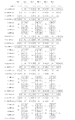
図14は、図8に示す画素ブロック804〜806を縮小処理する期間におけるフィルタ演算回路704の各種信号のタイミングチャートの一例を示す図である。
以下、図14を用いて、画素ブロック804〜806を縮小処理する際のフィルタ演算回路704による制御方法を説明する説明を行う。尚、図14に示す期間中の処理は、図13に示す期間中の処理において、前記画像データ入力信号への入力を以下の画素信号に置き換えた処理内容になる。
FIG. 14 is a diagram illustrating an example of a timing chart of various signals of the filter
Hereinafter, the control method by the filter
DATA_IN03信号(信号sig103)には、図8に示す行番号4の画素信号が入力される。DATA_IN13信号(信号sig113)には、図8に示す行番号5の画素信号が入力される。DATA_IN23信号(信号sig123)には、図8に示す行番号6の画素信号が入力される。DATA_IN33信号(信号sig133)には、図8に示す行番号7の画素信号が入力される。
図14中の期間B−1、B−3、B−5において、図13中の期間A−1、A−3、A−5と同様に、入力された画素信号がフリップフロップ回路1250〜1252により、順次伝搬される。
The pixel signal of
In the periods B-1, B-3, and B-5 in FIG. 14, the input pixel signals are converted into flip-flop circuits 1250 to 1252, as in the periods A-1, A-3, and A-5 in FIG. Are sequentially transmitted.
<画素ブロック804の縮小処理>
図14に示す期間B−2において、図8に示すRAW画像データの画素ブロック804内のR色の画素、G色の画素、B色の画素に対して順次、縮小処理が実行される。
ここで、前述の通り、図16に示す6×6画素単位のカラーフィルタ配列の持つ前記回転規則性より、図8に示す画素ブロック804の画素の色の並びは、画素ブロック802の画素の色の並びを左方向に90°回転した並びになる。
したがって、フィルタ係数読出し回路703は、画素ブロック802に対する各色画素用フィルタレジスタ(図10を参照)を左方向に90°回転させた位置のフィルタ係数を前記フィルタ係数信号に入力する。
期間B−2のR色の画素の縮小処理期間において、フィルタ係数読み出し回路703は、フィルタ係数レジスタ回路702より、画素ブロック802に対する前記R色画素用フィルタレジスタのフィルタ係数を読み出す(図10(a)を参照)。
<Reduction processing of pixel block 804>
In the period B-2 shown in FIG. 14, the reduction process is sequentially performed on the R color pixel, the G color pixel, and the B color pixel in the pixel block 804 of the RAW image data shown in FIG.
Here, as described above, due to the rotation regularity of the 6 × 6 pixel unit color filter array shown in FIG. 16, the arrangement of the pixel colors of the pixel block 804 shown in FIG. Are arranged in a sequence rotated 90 ° to the left.
Therefore, the filter
In the reduction processing period of the R color pixel in the period B-2, the filter
フィルタ係数信号FIL00〜FIL03(信号sig00〜03)には夫々、図10(a)に示す列番号3の4個のフィルタ係数を上から読み出した値(0,0,0,F_R23)が出力される。図14に示す例では、フィルタ係数1400が出力される。
フィルタ係数信号FIL10〜FIL13(信号sig10〜13)には夫々、図10(a)に示す列番号2の4個のフィルタ係数を上から読み出した値(0,F_R21,0,0)が出力される。図14に示す例では、フィルタ係数1401が出力される。
In the filter coefficient signals FIL00 to FIL03 (signals sig00 to 03), values (0, 0, 0, F_R23) obtained by reading the four filter coefficients of the
In the filter coefficient signals FIL10 to FIL13 (signals sig10 to 13), values (0, F_R21, 0, 0) obtained by reading the four filter coefficients of the
フィルタ係数信号FIL20〜FIL23(信号sig20〜23)には夫々、図10(a)に示す列番号1の4個のフィルタ係数を上から読み出した値(0,0,0,0)が出力される。図14に示す例では、フィルタ係数1402が出力される。
フィルタ係数信号FIL30〜FIL33(信号sig30〜33)には夫々、図10(a)に示す列番号0の4個のフィルタ係数を上から読み出した値(F_R20,0,F_R22,0)が出力される。図14に示す例では、フィルタ係数1403が出力される。
The filter coefficient signals FIL20 to FIL23 (signals sig20 to 23) are output with values (0, 0, 0, 0) obtained by reading the four filter coefficients of
The filter coefficient signals FIL30 to FIL33 (signals sig30 to 33) output values (F_R20, 0, F_R22, 0) obtained by reading the four filter coefficients of
画素値加算回路706は、各フィルタ係数と各画素値との積算の結果を加算し、図8に示す画素ブロック804の縮小処理後のR色の画素値R804として画像データ出力信号DATA_OUT(信号sig300)に出力する。画素値R804は、メモリI/F部105により、1/4に縮小処理されたR色の画像データとしてメモリ106に書き込まれる。
The pixel value addition circuit 706 adds the integration results of the filter coefficients and the pixel values, and outputs the image data output signal DATA_OUT (signal sig300) as the R pixel value R804 after the reduction processing of the pixel block 804 shown in FIG. ). The pixel value R804 is written into the
続く同期間B−2中のG色の画素の縮小処理期間において、フィルタ係数読み出し回路703は、フィルタ係数レジスタ回路702より、画素ブロック802に対する前記G色画素用フィルタレジスタのフィルタ係数を読み出す(図10(b)を参照)。
フィルタ係数信号FIL00〜FIL03(信号sig00〜03)には夫々、図10(b)に示す列番号3の4個のフィルタ係数を上から読み出した値(0,F_G23,0,0)が出力される。図14に示す例では、フィルタ係数1410が出力される。
フィルタ係数信号FIL10〜FIL13(信号sig10〜13)には夫々、図10(b)に示す列番号2の4個のフィルタ係数を上から読み出した値(F_G21,0,F_G25, F_G27)が出力される。図14に示す例では、フィルタ係数1411が出力される。
In the subsequent reduction period of the G color pixel during the synchronization period B-2, the filter
The filter coefficient signals FIL00 to FIL03 (signals sig00 to 03) are output with values (0, F_G23, 0, 0) obtained by reading the four filter coefficients of the
The filter coefficient signals FIL10 to FIL13 (signals sig10 to 13) output values (F_G21, 0, F_G25, F_G27) obtained by reading the four filter coefficients of
フィルタ係数信号FIL20〜FIL23(信号sig20〜23)には夫々、図10(b)に示す列番号1の4個のフィルタ係数を上から読み出した値(F_G20,0,F_G24, F_G26)が出力される。図14に示す例では、フィルタ係数1412が出力される。
フィルタ係数信号FIL30〜FIL33(信号sig30〜33)には夫々、図10(b)に示す列番号0の4個のフィルタ係数を上から読み出した値(0, F_G22, 0, 0)が出力される。図14に示す例では、フィルタ係数1413が出力される。
The filter coefficient signals FIL20 to FIL23 (signals sig20 to 23) output values (F_G20, 0, F_G24, F_G26) obtained by reading the four filter coefficients of the
The filter coefficient signals FIL30 to FIL33 (signals sig30 to 33) output values (0, F_G22, 0, 0) obtained by reading the four filter coefficients of
画素値加算回路706は、各フィルタ係数と各画素値との積算の結果を加算し、図8に示す画素ブロック804の縮小処理後のG色の画素値G804として画像データ出力信号DATA_OUT(信号sig300)に出力する。画素値G804は、メモリI/F部105により、1/4に縮小処理されたG色の画像データとしてメモリ106に書き込まれる。
The pixel value addition circuit 706 adds the integration results of the filter coefficients and the pixel values, and outputs the image data output signal DATA_OUT (signal sig300) as the G pixel value G804 after the reduction processing of the pixel block 804 shown in FIG. ). The pixel value G804 is written into the
続く同期間B−2中のB色の画素の縮小処理期間において、フィルタ係数読み出し回路703は、フィルタ係数レジスタ回路702より、画素ブロック802に対する前記B色画素用フィルタレジスタのフィルタ係数を読み出す(図10(c)を参照)。
フィルタ係数信号FIL00〜FIL03(信号sig00〜03)には夫々、図10(c)に示す列番号3の4個のフィルタ係数を上から読み出した値(F_B20,0,F_B22,0)が出力される。図14に示す例では、フィルタ係数1420が出力される。
フィルタ係数信号FIL10〜FIL13(信号sig10〜13)には夫々、図10(c)に示す列番号2の4個のフィルタ係数を上から読み出した値(0,0,0,0)が出力される。図14に示す例では、フィルタ係数1421が出力される。
In the subsequent B pixel reduction processing period during the synchronization period B-2, the filter
The filter coefficient signals FIL00 to FIL03 (signals sig00 to 03) are output with values (F_B20,0, F_B22,0) obtained by reading the four filter coefficients of
The filter coefficient signals FIL10 to FIL13 (signals sig10 to 13) are output with values (0, 0, 0, 0) obtained by reading the four filter coefficients of
フィルタ係数信号FIL20〜FIL23(信号sig20〜23)には夫々、図10(c)に示す列番号1の4個のフィルタ係数を上から読み出した値(0,F_B21,0,0)が出力される。図14に示す例では、フィルタ係数1422が出力される。
フィルタ係数信号FIL30〜FIL33(信号sig30〜33)には夫々、図10(c)に示す列番号0の4個のフィルタ係数を上から読み出した値(0, 0, 0, F_B23)が出力される。図14に示す例では、フィルタ係数1423が出力される。
The filter coefficient signals FIL20 to FIL23 (signals sig20 to 23) are output with values (0, F_B21, 0, 0) obtained by reading the four filter coefficients of
The filter coefficient signals FIL30 to FIL33 (signals sig30 to 33) are output with values (0, 0, 0, F_B23) obtained by reading the four filter coefficients of
画素値加算回路706は、各フィルタ係数と各画素値との積算の結果を加算し、図8に示す画素ブロック804の縮小処理後のB色の画素値B804として画像データ出力信号DATA_OUT(信号sig300)に出力する。画素値B804は、メモリI/F部105により、1/4に縮小処理されたB色の画像データとしてメモリ106に書き込まれる。
以上で、図8に示すRAW画像データの画素ブロック804内のR色の画素、G色の画素、及びB色の画素に対しての縮小処理が完了する。
The pixel value addition circuit 706 adds the integration results of the filter coefficients and the pixel values, and outputs the image data output signal DATA_OUT (signal sig300) as a B pixel value B804 after the reduction processing of the pixel block 804 shown in FIG. ). Pixel value B804 is written into
This completes the reduction processing for the R color pixel, the G color pixel, and the B color pixel in the pixel block 804 of the RAW image data shown in FIG.
<画素ブロック805の縮小処理>
図14に示す期間B−4において、図8に示すRAW画像データの画素ブロック805内のR色の画素、G色の画素、B色の画素に対して順次、縮小処理が実行される。
期間B−4のR色の画素の縮小処理期間において、フィルタ係数読み出し回路703は、フィルタ係数レジスタ回路702より、画素ブロック805に対する前記R色画素用フィルタレジスタのフィルタ係数を読み出す(図11(a)を参照)。
<Reduction processing of
In the period B-4 shown in FIG. 14, the reduction process is sequentially performed on the R color pixel, the G color pixel, and the B color pixel in the
During the reduction process of the R color pixel in period B-4, the filter
フィルタ係数信号FIL00〜FIL03(信号sig00〜03)には夫々、図11(a)に示す行番号0の4個のフィルタ係数を左から読み出した値(0,F_R30,0,0)が出力される。図14に示す例では、フィルタ係数1430が出力される。
フィルタ係数信号FIL10〜FIL13(信号sig10〜13)には夫々、図11(a)に示す行番号1の4個のフィルタ係数を左から読み出した値(0,0,0,F_R31)が出力される。図14に示す例では、フィルタ係数1431が出力される。
In the filter coefficient signals FIL00 to FIL03 (signals sig00 to 03), values (0, F_R30, 0, 0) obtained by reading the four filter coefficients of the
In the filter coefficient signals FIL10 to FIL13 (signals sig10 to 13), values (0, 0, 0, F_R31) obtained by reading the four filter coefficients of the
フィルタ係数信号FIL20〜FIL23(信号sig20〜23)には夫々、図11(a)に示す行番号2の4個のフィルタ係数を左から読み出した値(F_R32,0,0,0)が出力される。図14に示す例では、フィルタ係数1432が出力される。
フィルタ係数信号FIL30〜FIL33(信号sig30〜33)には夫々、図11(a)に示す行番号3の4個のフィルタ係数を左から読み出した値(0,0,F_R33,0)が出力される。図14に示す例では、フィルタ係数1433が出力される。
The filter coefficient signals FIL20 to FIL23 (signals sig20 to 23) are output with values (F_R32,0,0,0) obtained by reading the four filter coefficients of the
The filter coefficient signals FIL30 to FIL33 (signals sig30 to 33) are output with values (0, 0, F_R33, 0) obtained by reading the four filter coefficients of
画素値加算回路706は、各フィルタ係数と各画素値との積算の結果を加算し、図8に示す画素ブロック805の縮小処理後のR色の画素値R805として画像データ出力信号DATA_OUT(信号sig300)に出力する。画素値R805は、メモリI/F部105により、1/4に縮小処理されたR色の画像データとしてメモリ106に書き込まれる。
The pixel value addition circuit 706 adds the integration results of the filter coefficients and the pixel values, and outputs the image data output signal DATA_OUT (signal sig300) as the R color pixel value R805 after the reduction processing of the
続く同期間B−4中のG色の画素の縮小処理期間において、フィルタ係数読み出し回路703は、フィルタ係数レジスタ回路702より、画素ブロック805に対する前記G色画素用フィルタレジスタのフィルタ係数を読み出す(図11(b)を参照)。
フィルタ係数信号FIL00〜FIL03(信号sig00〜03)には夫々、図11(b)に示す行番号0の4個のフィルタ係数を左から読み出した値(F_G30,0,0, F_G31)が出力される。図14に示す例では、フィルタ係数1440が出力される。
フィルタ係数信号FIL10〜FIL13(信号sig10〜13)には夫々、図11(b)に示す行番号1の4個のフィルタ係数を左から読み出した値(0,F_G32, F_G33,0)が出力される。図14に示す例では、フィルタ係数1441が出力される。
In the subsequent reduction processing period of the G color pixel during the synchronization period B-4, the filter
The filter coefficient signals FIL00 to FIL03 (signals sig00 to 03) output values (F_G30, 0, 0, F_G31) obtained by reading the four filter coefficients of
The filter coefficient signals FIL10 to FIL13 (signals sig10 to 13) are output with values (0, F_G32, F_G33,0) obtained by reading the four filter coefficients of
フィルタ係数信号FIL20〜FIL23(信号sig20〜23)には夫々、図11(b)に示す行番号2の4個のフィルタ係数を左から読み出した値(0,F_G34, F_G35,0)が出力される。図14に示す例では、フィルタ係数1442が出力される。
フィルタ係数信号FIL30〜FIL33(信号sig30〜33)には夫々、図11(b)に示す行番号3の4個のフィルタ係数を左から読み出した値(F_G36,0,0,F_G37)が出力される。図14に示す例では、フィルタ係数1443が出力される。
The filter coefficient signals FIL20 to FIL23 (signals sig20 to 23) output values (0, F_G34, F_G35, 0) obtained by reading the four filter coefficients of
The filter coefficient signals FIL30 to FIL33 (signals sig30 to 33) output values (F_G36, 0, 0, F_G37) obtained by reading the four filter coefficients of the
画素値加算回路706は、各フィルタ係数と各画素値との積算の結果を加算し、図8に示す画素ブロック804の縮小処理後のG色の画素値G805として画像データ出力信号DATA_OUT(信号sig300)に出力する。画素値G805は、メモリI/F部105により、1/4に縮小処理されたG色の画像データとしてメモリ106に書き込まれる。
The pixel value adding circuit 706 adds the results of integration of the filter coefficients and the pixel values, and outputs the image data output signal DATA_OUT (signal sig300) as a G pixel value G805 after the reduction processing of the pixel block 804 shown in FIG. ). The pixel value G805 is written in the
続く同期間B−4中のB色の画素の縮小処理期間において、フィルタ係数読み出し回路703は、フィルタ係数レジスタ回路702より、画素ブロック805に対する前記B色画素用フィルタレジスタのフィルタ係数を読み出す(図11(c)を参照)。
フィルタ係数信号FIL00〜FIL03(信号sig00〜03)には夫々、図11(c)に示す行番号0の4個のフィルタ係数を左から読み出した値(0,0,F_B30,0)が出力される。図14に示す例では、フィルタ係数1450が出力される。
フィルタ係数信号FIL10〜FIL13(信号sig10〜13)には夫々、図11(c)に示す行番号1の4個のフィルタ係数を左から読み出した値(F_B31,0,0,0)が出力される。図14に示す例では、フィルタ係数1451が出力される。
In the subsequent B pixel reduction processing period during synchronization B-4, the filter
The filter coefficient signals FIL00 to FIL03 (signals sig00 to 03) are output with values (0,0, F_B30,0) obtained by reading the four filter coefficients of
In the filter coefficient signals FIL10 to FIL13 (signals sig10 to 13), values (F_B31, 0, 0, 0) obtained by reading the four filter coefficients of the
フィルタ係数信号FIL20〜FIL23(信号sig20〜23)には夫々、図11(c)に示す行番号2の4個のフィルタ係数を左から読み出した値(0,0,0,F_B32)が出力される。図14に示す例では、フィルタ係数1452が出力される。
フィルタ係数信号FIL30〜FIL33(信号sig30〜33)には夫々、図11(c)に示す行番号3の4個のフィルタ係数を左から読み出した値(0, F_B33, 0, 0)が出力される。図14に示す例では、フィルタ係数1453が出力される。
The filter coefficient signals FIL20 to FIL23 (signals sig20 to 23) are output with values (0, 0, 0, F_B32) obtained by reading the four filter coefficients of the
The filter coefficient signals FIL30 to FIL33 (signals sig30 to 33) are output with values (0, F_B33, 0, 0) obtained by reading the four filter coefficients of
画素値加算回路706は、各フィルタ係数と各画素値との積算の結果を加算し、図8に示す画素ブロック805の縮小処理後のB色の画素値B805として画像データ出力信号DATA_OUT(信号sig300)に出力する。画素値B805は、メモリI/F部105により、1/4に縮小処理されたB色の画像データとしてメモリ106に書き込まれる。
以上で、図8に示すRAW画像データの画素ブロック805内のR色の画素、G色の画素、及びB色の画素に対しての縮小処理が完了する。
The pixel value addition circuit 706 adds the integration results of the filter coefficients and the pixel values, and outputs the image data output signal DATA_OUT (signal sig300) as a B pixel value B805 after the reduction processing of the
Thus, the reduction processing for the R color pixel, the G color pixel, and the B color pixel in the
<画素ブロック806の縮小処理>
図14に示す期間B−6において、図8に示すRAW画像データの画素ブロック806内のR色の画素、G色の画素、B色の画素に対して順次、縮小処理が実行される。
ここで、前述の通り、図16に示す6×6画素単位のカラーフィルタ配列の持つ前記回転規則性より、図8に示す画素ブロック806の画素の色の並びは、画素ブロック802の画素の色の並びを右方向に90°回転した並びになる。
したがって、フィルタ係数読出し回路703は、画素ブロック802に対する各色画素用フィルタレジスタ(図10を参照)を右方向に90°回転させた位置のフィルタ係数を前記フィルタ係数信号に入力する。
期間B−6のR色の画素の縮小処理期間において、フィルタ係数読み出し回路703は、フィルタ係数レジスタ回路702より、画素ブロック802に対する前記R色画素用フィルタレジスタのフィルタ係数を読み出す(図10(a)を参照)。
<Reduction processing of
In a period B-6 shown in FIG. 14, the reduction processing is sequentially performed on the R color pixel, the G color pixel, and the B color pixel in the
Here, as described above, due to the rotation regularity of the 6 × 6 pixel unit color filter array shown in FIG. 16, the arrangement of the pixel colors of the
Therefore, the filter
In the reduction processing period of the R color pixel in the period B-6, the filter
フィルタ係数信号FIL00〜FIL03(信号sig00〜03)には夫々、図10(a)に示す列番号0の4個のフィルタ係数を下から読み出した値(0,F_R22,0, F_R20)が出力される。図14に示す例では、フィルタ係数1460が出力される。
フィルタ係数信号FIL10〜FIL13(信号sig10〜13)には夫々、図10(a)に示す列番号1の4個のフィルタ係数を下から読み出した値(0,0,0,0)が出力される。図14に示す例では、フィルタ係数1461が出力される。
The filter coefficient signals FIL00 to FIL03 (signals sig00 to 03) output values (0, F_R22, 0, F_R20) obtained by reading the four filter coefficients of
The filter coefficient signals FIL10 to FIL13 (signals sig10 to 13) are output with values (0, 0, 0, 0) obtained by reading the four filter coefficients of
フィルタ係数信号FIL20〜FIL23(信号sig20〜23)には夫々、図10(a)に示す列番号2の4個のフィルタ係数を下から読み出した値(0,0,F_R21,0)が出力される。図14に示す例では、フィルタ係数1462が出力される。
フィルタ係数信号FIL30〜FIL33(信号sig30〜33)には夫々、図10(a)に示す列番号3の4個のフィルタ係数を下から読み出した値(F_R23,0,0,0)が出力される。図14に示す例では、フィルタ係数1463が出力される。
The filter coefficient signals FIL20 to FIL23 (signals sig20 to 23) are output with values (0, 0, F_R21, 0) obtained by reading the four filter coefficients of
The filter coefficient signals FIL30 to FIL33 (signals sig30 to 33) are output with values (F_R23, 0, 0, 0) obtained by reading the four filter coefficients of
画素値加算回路706は、各フィルタ係数と各画素値との積算の結果を加算し、図8に示す画素ブロック806の縮小処理後のR色の画素値R806として画像データ出力信号DATA_OUT(信号sig300)に出力する。画素値R806は、メモリI/F部105により、1/4に縮小処理されたR色の画像データとしてメモリ106に書き込まれる。
The pixel value addition circuit 706 adds the results of integration of the filter coefficients and the pixel values, and outputs the image data output signal DATA_OUT (signal sig300) as an R color pixel value R806 after the reduction processing of the
続く同期間B−6中のG色の画素の縮小処理期間において、フィルタ係数読み出し回路703は、フィルタ係数レジスタ回路702より、画素ブロック802に対する前記G色画素用フィルタレジスタのフィルタ係数を読み出す(図10(b)を参照)。
フィルタ係数信号FIL00〜FIL03(信号sig00〜03)には夫々、図10(b)に示す列番号0の4個のフィルタ係数を下から読み出した値(0,0,F_G22,0)が出力される。図14に示す例では、フィルタ係数1470が出力される。
フィルタ係数信号FIL10〜FIL13(信号sig10〜13)には夫々、図10(b)に示す列番号1の4個のフィルタ係数を下から読み出した値(F_G26,F_G24,0,F_G20)が出力される。図14に示す例では、フィルタ係数1471が出力される。
In the subsequent reduction processing period of the G color pixel during the synchronization period B-6, the filter
The filter coefficient signals FIL00 to FIL03 (signals sig00 to 03) output values (0, 0, F_G22, 0) obtained by reading the four filter coefficients of
The filter coefficient signals FIL10 to FIL13 (signals sig10 to 13) output values (F_G26, F_G24, 0, F_G20) obtained by reading the four filter coefficients of
フィルタ係数信号FIL20〜FIL23(信号sig20〜23)には夫々、図10(b)に示す列番号2の4個のフィルタ係数を下から読み出した値(F_G27,F_G25,0,F_G21)が出力される。図14に示す例では、フィルタ係数1472が出力される。
フィルタ係数信号FIL30〜FIL33(信号sig30〜33)には夫々、図10(b)に示す列番号3の4に示すフィルタ係数を下から読み出した値(0,0,F_G23,0)が出力される。図14に示す例では、フィルタ係数1473が出力される。
The filter coefficient signals FIL20 to FIL23 (signals sig20 to 23) are output with values (F_G27, F_G25, 0, F_G21) obtained by reading the four filter coefficients of
The filter coefficient signals FIL30 to FIL33 (signals sig30 to 33) are output with values (0, 0, F_G23, 0) obtained by reading the filter coefficient indicated by 4 in
画素値加算回路706は、各フィルタ係数と各画素値との積算の結果を加算し、図8に示す画素ブロック806の縮小処理後のG色の画素値G806として画像データ出力信号DATA_OUT(信号sig300)に出力する。画素値G806は、メモリI/F部105により、1/4に縮小処理されたG色の画像データとしてメモリ106に書き込まれる。
The pixel value addition circuit 706 adds the integration results of the filter coefficients and the pixel values, and outputs the image data output signal DATA_OUT (signal sig300) as a G pixel value G806 after the reduction processing of the
続く同期間B−6のB色の画素の縮小処理期間において、フィルタ係数読み出し回路703は、フィルタ係数レジスタ回路702より、画素ブロック802に対する前記B色画素用フィルタレジスタのフィルタ係数を読み出す(図10(c)を参照)。
フィルタ係数信号FIL00〜FIL03(信号sig00〜03)には夫々、図10(c)に示す列番号0の4個のフィルタ係数を下から読み出した値(F_B23,0,0,0)が出力される。図14に示す例では、フィルタ係数1480が出力される。
フィルタ係数信号FIL10〜FIL13(信号sig10〜13)には夫々、図10(c)に示す列番号1の4個のフィルタ係数を下から読み出した値(0,0,F_B21,0)が出力される。図14に示す例では、フィルタ係数1481が出力される。
In the subsequent B pixel reduction processing period of B-6, the filter
The filter coefficient signals FIL00 to FIL03 (signals sig00 to 03) are output with values (F_B23,0,0,0) obtained by reading the four filter coefficients of
The filter coefficient signals FIL10 to FIL13 (signals sig10 to 13) are output with values (0, 0, F_B21, 0) obtained by reading the four filter coefficients of
フィルタ係数信号FIL20〜FIL23(信号sig20〜23)には夫々、図10(c)に示す列番号2の4個のフィルタ係数を下から読み出した値(0,0,0,0)が出力される。図14に示す例では、フィルタ係数1482が出力される。
フィルタ係数信号FIL30〜FIL33(信号sig30〜33)には夫々、図10(c)に示す列番号3の4個のフィルタ係数を下から読み出した値(0,F_B22,0,F_B20)が出力される。図14に示す例では、フィルタ係数1483が出力される。
The filter coefficient signals FIL20 to FIL23 (signals sig20 to 23) are output with values (0, 0, 0, 0) obtained by reading the four filter coefficients of
The filter coefficient signals FIL30 to FIL33 (signals sig30 to 33) output values (0, F_B22, 0, F_B20) obtained by reading the four filter coefficients of the
画素値加算回路706は、各フィルタ係数と各画素値との積算の結果を加算し、図8に示す画素ブロック806の縮小処理後のB色の画素値B806として画像データ出力信号DATA_OUT(信号sig300)に出力する。画素値B806は、メモリI/F部105により、1/4に縮小処理されたB色の画像データとしてメモリ106に書き込まれる。
以上で、図8に示すRAW画像データの画素ブロック806内のR色の画素、G色の画素、及びB色の画素に対しての縮小処理が完了する。
The pixel value addition circuit 706 adds the integration results of the filter coefficients and the pixel values, and outputs the image data output signal DATA_OUT (signal sig300) as a B pixel value B806 after the reduction processing of the
Thus, the reduction process for the R color pixel, the G color pixel, and the B color pixel in the
図15は、図8に示す画素ブロック807〜809を縮小処理する期間におけるフィルタ演算回路704の各種信号のタイミングチャートの一例を示す図である。
以下、図15を用いて、画素ブロック807〜809を縮小処理する際のフィルタ演算回路704による制御方法を説明する説明を行う。尚、図15に示す期間中の処理は、図13に示す期間中の処理において、前記画像データ入力信号への入力を以下の画素信号に置き換えた処理内容になる。
FIG. 15 is a diagram illustrating an example of a timing chart of various signals of the filter
Hereinafter, the control method by the filter
DATA_IN03信号(信号sig103)には、図8に示す行番号8の画素信号が入力される。DATA_IN13信号(信号sig113)には、図8に示す行番号9の画素信号が入力される。DATA_IN23信号(信号sig123)には、図8に示す行番号10の画素信号が入力される。DATA_IN33信号(信号sig133)には、図8に示す行番号11の画素信号が入力される。
図15中の期間C−1、C−3、C−5において、図13中の期間A−1、A−3、A−5と同様に、入力された画素信号がフリップフロップ回路1250〜1252により、順次伝搬される。
The pixel signal of
In the periods C-1, C-3, and C-5 in FIG. 15, the input pixel signals are converted into flip-flop circuits 1250 to 1252, as in the periods A-1, A-3, and A-5 in FIG. Are sequentially transmitted.
<画素ブロック807の縮小処理>
図15に示す期間C−2において、図8に示すRAW画像データの画素ブロック807内のR色の画素、G色の画素、B色の画素に対して順次、縮小処理が実行される。
ここで、前述の通り、図16に示す6×6画素単位のカラーフィルタ配列の持つ前記回転規則性より、図8に示す画素ブロック807の画素の色の並びは、画素ブロック801の画素の色の並びを左方向に90°回転した並びになる。
したがって、フィルタ係数読出し回路703は、画素ブロック801に対する各色画素用フィルタレジスタ(図9を参照)を左方向に90°回転させた位置のフィルタ係数を前記フィルタ係数信号に入力する。
期間C−2のR色の画素の縮小処理期間において、フィルタ係数読み出し回路703は、フィルタ係数レジスタ回路702より、画素ブロック801に対する前記R色画素用フィルタレジスタのフィルタ係数を読み出す(図9(a)を参照)。
<Reduction processing of pixel block 807>
In a period C-2 shown in FIG. 15, the reduction processing is sequentially performed on the R color pixel, the G color pixel, and the B color pixel in the pixel block 807 of the RAW image data shown in FIG.
Here, as described above, due to the rotation regularity of the 6 × 6 pixel unit color filter array shown in FIG. 16, the arrangement of the pixel colors of the pixel block 807 shown in FIG. This is a sequence of 90 ° rotated leftward.
Therefore, the filter
In the reduction process period of the R color pixel in the period C-2, the filter
フィルタ係数信号FIL00〜FIL03(信号sig00〜03)には夫々、図9(a)に示す列番号3の4個のフィルタ係数を上から読み出した値(0,0,0,0)が出力される。図15に示す例では、フィルタ係数1500が出力される。
フィルタ係数信号FIL10〜FIL13(信号sig10〜13)には夫々、図9(a)に示す列番号2のフィルタ係数を上から読み出した値(0,F_R11,0,0)が出力される。図15に示す例では、フィルタ係数1501が出力される。
In filter coefficient signals FIL00 to FIL03 (signals sig00 to 03), values (0, 0, 0, 0) obtained by reading the four filter coefficients of
The filter coefficient signals FIL10 to FIL13 (signals sig10 to 13) output values (0, F_R11, 0, 0) obtained by reading the filter coefficient of
フィルタ係数信号FIL20〜FIL23(信号sig20〜23)には夫々、図9(a)に示す列番号1の4個のフィルタ係数を上から読み出した値(0,0,0,F_R12)が出力される。図15に示す例では、フィルタ係数1502が出力される。
フィルタ係数信号FIL30〜FIL33(信号sig30〜33)には夫々、図9(a)に示す列番号0の4個のフィルタ係数を上から読み出した値(0,F_R10,0,0)が出力される。図15に示す例では、フィルタ係数1503が出力される。
The filter coefficient signals FIL20 to FIL23 (signals sig20 to 23) are output with values (0, 0, 0, F_R12) obtained by reading the four filter coefficients of
The filter coefficient signals FIL30 to FIL33 (signals sig30 to 33) are output with values (0, F_R10, 0, 0) obtained by reading the four filter coefficients of
画素値加算回路706は、各フィルタ係数と各画素値との積算の結果を加算し、図8に示す画素ブロック807の縮小処理後のR色の画素値R807として画像データ出力信号DATA_OUT(信号sig300)に出力する。画素値R807は、メモリI/F部105により、1/4に縮小処理されたR色の画像データとしてメモリ106に書き込まれる。
The pixel value addition circuit 706 adds the integration results of the filter coefficients and the pixel values, and outputs the image data output signal DATA_OUT (signal sig300) as the R pixel value R807 after the reduction processing of the pixel block 807 shown in FIG. ). The pixel value R807 is written in the
続く同期間C−2中のG色の画素の縮小処理期間において、フィルタ係数読み出し回路703は、フィルタ係数レジスタ回路702より、画素ブロック801に対する前記G色画素用フィルタレジスタのフィルタ係数を読み出す(図9(b)を参照)。
フィルタ係数信号FIL00〜FIL03(信号sig00〜03)には夫々、図9(b)に示す列番号3の4個のフィルタ係数を上から読み出した値(F_G12,0,F_G16, F_G19)が出力される。図15に示す例では、フィルタ係数1510が出力される。
フィルタ係数信号FIL10〜FIL13(信号sig10〜13)には夫々、図9(b)に示す列番号2の4個のフィルタ係数を上から読み出した値(F_G11,0,F_G15, F_G18)が出力される。図15に示す例では、フィルタ係数1511が出力される。
In the subsequent reduction processing period of the G color pixel during the synchronization period C-2, the filter
The filter coefficient signals FIL00 to FIL03 (signals sig00 to 03) output values (F_G12, 0, F_G16, F_G19) obtained by reading the four filter coefficients of the
The filter coefficient signals FIL10 to FIL13 (signals sig10 to 13) output values (F_G11, 0, F_G15, F_G18) obtained by reading the four filter coefficients of
フィルタ係数信号FIL20〜FIL23(信号sig20〜23)には夫々、図9(b)に示す列番号1の4個のフィルタ係数を上から読み出した値(0,F_G13,0,0)が出力される。図15に示す例では、フィルタ係数1512が出力される。
フィルタ係数信号FIL30〜FIL33(信号sig30〜33)には夫々、図9(b)に示す列番号0の4個のフィルタ係数を上から読み出した値(F_G10,0, F_G14, F_G17)が出力される。図15に示す例では、フィルタ係数1513が出力される。
The filter coefficient signals FIL20 to FIL23 (signals sig20 to 23) are output with values (0, F_G13, 0, 0) obtained by reading the four filter coefficients of
The filter coefficient signals FIL30 to FIL33 (signals sig30 to 33) output values (F_G10, 0, F_G14, F_G17) obtained by reading the four filter coefficients of
画素値加算回路706は、各フィルタ係数と各画素値との積算の結果を加算し、図8に示す画素ブロック807の縮小処理後のG色の画素値G807として画像データ出力信号DATA_OUT(信号sig300)に出力する。画素値G807は、メモリI/F部105により、1/4に縮小処理されたG色の画像データとしてメモリ106に書き込まれる。
The pixel value addition circuit 706 adds the integration results of the filter coefficients and the pixel values, and outputs the image data output signal DATA_OUT (signal sig300) as the G pixel value G807 after the reduction processing of the pixel block 807 shown in FIG. ). The pixel value G807 is written in the
続く同期間C−2中のB色の画素の縮小処理期間において、フィルタ係数読み出し回路703は、フィルタ係数レジスタ回路702より、画素ブロック801に対する前記B色画素用フィルタレジスタのフィルタ係数を読み出す(図9(c)を参照)。
フィルタ係数信号FIL00〜FIL03(信号sig00〜03)には夫々、図9(c)に示す列番号3の4個のフィルタ係数を上から読み出した値(0,F_B11,0,0)が出力される。図15に示す例では、フィルタ係数1520が出力される。
フィルタ係数信号FIL10〜FIL13(信号sig10〜13)には夫々、図9(c)に示す列番号2の4個のフィルタ係数を上から読み出した値(0,0,0,0)が出力される。図15に示す例では、フィルタ係数1521が出力される。
In the subsequent B pixel reduction processing period during the synchronization period C-2, the filter
The filter coefficient signals FIL00 to FIL03 (signals sig00 to 03) output values (0, F_B11, 0, 0) obtained by reading the four filter coefficients of
The filter coefficient signals FIL10 to FIL13 (signals sig10 to 13) are output with values (0, 0, 0, 0) obtained by reading the four filter coefficients of
フィルタ係数信号FIL20〜FIL23(信号sig20〜23)には夫々、図9(c)に示す列番号1の4個のフィルタ係数を上から読み出した値(F_B10,0,F_B12,0)が出力される。図15に示す例では、フィルタ係数1522が出力される。
フィルタ係数信号FIL30〜FIL33(信号sig30〜33)には夫々、図9(c)に示す列番号0の4個のフィルタ係数を上から読み出した値(0,0,0,0)が出力される。図15に示す例では、フィルタ係数1523が出力される。
The filter coefficient signals FIL20 to FIL23 (signals sig20 to 23) output values (F_B10,0, F_B12,0) obtained by reading the four filter coefficients of
The filter coefficient signals FIL30 to FIL33 (signals sig30 to 33) are output with values (0, 0, 0, 0) obtained by reading the four filter coefficients of
画素値加算回路706は、各フィルタ係数と各画素値との積算の結果を加算し、図8に示す画素ブロック807の縮小処理後のB色の画素値B807として画像データ出力信号DATA_OUT(信号sig300)に出力する。画素値B807は、メモリI/F部105により、1/4に縮小処理されたB色の画像データとしてメモリ106に書き込まれる。
以上で、図8に示すRAW画像データの画素ブロック807内のR色の画素、G色の画素、及びB色の画素に対しての縮小処理が完了する。
The pixel value addition circuit 706 adds the results of integration of the filter coefficients and the pixel values, and outputs the image data output signal DATA_OUT (signal sig300) as a B pixel value B807 after the reduction processing of the pixel block 807 shown in FIG. ). The pixel value B807 is written into the
Thus, the reduction processing for the R color pixel, the G color pixel, and the B color pixel in the pixel block 807 of the RAW image data shown in FIG. 8 is completed.
<画素ブロック808の縮小処理>
図15に示す期間C−4において、図8に示すRAW画像データの画素ブロック808内のR色の画素、G色の画素、B色の画素に対して順次、縮小処理が実行される。
ここで、前述の通り、図16に示す6×6画素単位のカラーフィルタ配列の持つ前記回転規則性より、図8に示す画素ブロック808の画素の色の並びは画素ブロック802の画素の色の並びを180°回転した並びになる。
したがって、フィルタ係数読出し回路703は、画素ブロック802に対する各色画素用フィルタレジスタ(図10を参照)を180°回転させた位置のフィルタ係数を前記フィルタ係数信号に入力する。
期間C−4のR色の画素の縮小処理期間において、フィルタ係数読み出し回路703は、フィルタ係数レジスタ回路702より、画素ブロック802に対する前記R色画素用フィルタレジスタのフィルタ係数を読み出す(図10(a)を参照)。
<Reduction processing of
In a period C-4 illustrated in FIG. 15, reduction processing is sequentially performed on the R color pixel, the G color pixel, and the B color pixel in the
Here, as described above, due to the rotation regularity of the 6 × 6 pixel unit color filter array shown in FIG. 16, the arrangement of the pixel colors of the
Therefore, the filter
In the reduction processing period of the R color pixel in the period C-4, the filter
フィルタ係数信号FIL00〜FIL03(信号sig00〜03)には夫々、図10(a)に示す行番号3の4個のフィルタ係数を右から読み出した値(F_R23,0,0,0)が出力される。図15に示す例では、フィルタ係数1530が出力される。
フィルタ係数信号FIL10〜FIL13(信号sig10〜13)には夫々、図10(a)に示す行番号2の4個のフィルタ係数を右から読み出した値(0,0,0,F_R22)が出力される。図15に示す例では、フィルタ係数1531が出力される。
The filter coefficient signals FIL00 to FIL03 (signals sig00 to 03) output the values (F_R23, 0, 0, 0) obtained by reading the four filter coefficients of the
In the filter coefficient signals FIL10 to FIL13 (signals sig10 to 13), values (0, 0, 0, F_R22) obtained by reading the four filter coefficients of the
フィルタ係数信号FIL20〜FIL23(信号sig20〜23)には夫々、図10(a)に示す行番号1の4個のフィルタ係数を右から読み出した値(0,F_R21,0,0)が出力される。図15に示す例では、フィルタ係数1532が出力される。
フィルタ係数信号FIL30〜FIL33(信号sig30〜33)には夫々、図10(a)に示す行番号0の4個のフィルタ係数を右から読み出した値(0,0,0,F_R20)が出力される。図15に示す例では、フィルタ係数1533が出力される。
The filter coefficient signals FIL20 to FIL23 (signals sig20 to 23) are output with values (0, F_R21, 0, 0) obtained by reading the four filter coefficients of
The filter coefficient signals FIL30 to FIL33 (signals sig30 to 33) are output with values (0, 0, 0, F_R20) obtained by reading the four filter coefficients of
画素値加算回路706は、各フィルタ係数と各画素値との積算の結果を加算し、図8に示す画素ブロック808の縮小処理後のR色の画素値R808として画像データ出力信号DATA_OUT(信号sig300)に出力する。画素値R808は、メモリI/F部105により、1/4に縮小処理されたR色の画像データとしてメモリ106に書き込まれる。
The pixel value adding circuit 706 adds the results of integration of the filter coefficients and the pixel values, and outputs the image data output signal DATA_OUT (signal sig300) as the R pixel value R808 after the reduction processing of the
続く同期間C−4中のG色の画素の縮小処理期間において、フィルタ係数読み出し回路703は、フィルタ係数レジスタ回路702より、画素ブロック802に対する前記G色画素用フィルタレジスタのフィルタ係数を読み出す(図10(b)を参照)。
フィルタ係数信号FIL00〜FIL03(信号sig00〜03)には夫々、図10(b)に示す行番号3の4個のフィルタ係数を右から読み出した値(0,F_G27,F_G26,0)が出力される。図15に示す例では、フィルタ係数1540が出力される。
フィルタ係数信号FIL10〜FIL13(信号sig10〜13)には夫々、図10(b)に示す行番号2の4個のフィルタ係数を右から読み出した値(0,F_G25,F_G24,0)が出力される。図15に示す例では、フィルタ係数1541が出力される。
In the subsequent reduction processing period of the G color pixel during the synchronization period C-4, the filter
The filter coefficient signals FIL00 to FIL03 (signals sig00 to 03) output values (0, F_G27, F_G26, 0) obtained by reading the four filter coefficients of
The filter coefficient signals FIL10 to FIL13 (signals sig10 to 13) are output with values (0, F_G25, F_G24, 0) obtained by reading the four filter coefficients of the
フィルタ係数信号FIL20〜FIL23(信号sig20〜23)には夫々、図10(b)に示す行番号1の4個のフィルタ係数を右から読み出した値(F_G23,0,0, F_G22)が出力される。図15に示す例では、フィルタ係数1542が出力される。
フィルタ係数信号FIL30〜FIL33(信号sig30〜33)には夫々、図10(b)に示す行番号0の4個のフィルタ係数を右から読み出した値(0,F_G21,F_G20,0)が出力される。図15に示す例では、フィルタ係数1543が出力される。
The filter coefficient signals FIL20 to FIL23 (signals sig20 to 23) output values (F_G23,0,0, F_G22) obtained by reading the four filter coefficients of the
The filter coefficient signals FIL30 to FIL33 (signals sig30 to 33) output values (0, F_G21, F_G20, 0) obtained by reading the four filter coefficients of
画素値加算回路706は、各フィルタ係数と各画素値との積算の結果を加算し、図8に示す画素ブロック808の縮小処理後のG色の画素値G808として画像データ出力信号DATA_OUT(信号sig300)に出力する。画素値G808は、メモリI/F部105により、1/4に縮小処理されたG色の画像データとしてメモリ106に書き込まれる。
The pixel value addition circuit 706 adds the integration results of the filter coefficients and the pixel values, and outputs the image data output signal DATA_OUT (signal sig300) as the G pixel value G808 after the reduction processing of the
続く同期間C−4中のB色の画素の縮小処理期間において、フィルタ係数読み出し回路703は、フィルタ係数レジスタ回路702より、画素ブロック802に対する前記B色画素用フィルタレジスタのフィルタ係数を読み出す(図10(c)を参照)。
フィルタ係数信号FIL00〜FIL03(信号sig00〜03)には夫々、図10(c)に示す行番号3の4個のフィルタ係数を右から読み出した値(0,0,0,F_B23)が出力される。図15に示す例では、フィルタ係数1550が出力される。
フィルタ係数信号FIL10〜FIL13(信号sig10〜13)には夫々、図10(c)に示す行番号2の4個のフィルタ係数を右から読み出した値(F_B22,0,0,0)が出力される。図15に示す例では、フィルタ係数1551が出力される。
In the subsequent reduction processing period of the B color pixel during the synchronization period C-4, the filter
In the filter coefficient signals FIL00 to FIL03 (signal sig00 to 03), values (0, 0, 0, F_B23) obtained by reading the four filter coefficients of the
The filter coefficient signals FIL10 to FIL13 (signals sig10 to 13) are output with values (F_B22, 0, 0, 0) obtained by reading the four filter coefficients of the
フィルタ係数信号FIL20〜FIL23(信号sig20〜23)には夫々、図10(c)に示す行番号1の4個のフィルタ係数を右から読み出した値(0,0,F_B21,0)が出力される。図15に示す例では、フィルタ係数1552が出力される。
フィルタ係数信号FIL30〜FIL33(信号sig30〜33)には夫々、図10(c)に示す行番号0の4個のフィルタ係数を右から読み出した値(F_B20,0,0,0)が出力される。図15に示す例では、フィルタ係数1553が出力される。
The filter coefficient signals FIL20 to FIL23 (signals sig20 to 23) output values (0, 0, F_B21, 0) obtained by reading the four filter coefficients of
The filter coefficient signals FIL30 to FIL33 (signals sig30 to 33) output values (F_B20, 0, 0, 0) obtained by reading the four filter coefficients of
画素値加算回路706は、各フィルタ係数と各画素値との積算の結果を加算し、図8に示す画素ブロック808の縮小処理後のB色の画素値B808として画像データ出力信号DATA_OUT(信号sig300)に出力する。画素値B808は、メモリI/F部105により、1/4に縮小処理されたB色の画像データとしてメモリ106に書き込まれる。
以上で、図8に示すRAW画像データの画素ブロック808内のR色の画素、G色の画素、及びB色の画素に対しての縮小処理が完了する。
The pixel value addition circuit 706 adds the integration results of the filter coefficients and the pixel values, and outputs the image data output signal DATA_OUT (signal sig300) as a B pixel value B808 after the reduction processing of the
This completes the reduction processing for the R color pixel, the G color pixel, and the B color pixel in the
<画素ブロック809の縮小処理>
図15に示す期間C−6において、図8に示すRAW画像データの画素ブロック809内のR色の画素、G色の画素、B色の画素に対して順次、縮小処理が実行される。
ここで、前述の通り、図16に示す6×6画素単位のカラーフィルタ配列の持つ前記回転規則性より、図8に示す画素ブロック809の画素の色の並びは、画素ブロック801の画素の色の並びを180°回転した並びになる。
したがって、フィルタ係数読出し回路703は、画素ブロック801に対する各色画素用フィルタレジスタ(図9を参照)を180°回転させた位置のフィルタ係数を前記フィルタ係数信号に入力する。
期間C−6のR色の画素の縮小処理期間において、フィルタ係数読み出し回路703は、フィルタ係数レジスタ回路702より、画素ブロック801に対する前記R色画素用フィルタレジスタのフィルタ係数を読み出す(図9(a)を参照)。
<Reduction processing of
In a period C-6 shown in FIG. 15, the reduction process is sequentially performed on the R color pixel, the G color pixel, and the B color pixel in the
Here, as described above, due to the rotation regularity of the 6 × 6 pixel unit color filter array shown in FIG. 16, the arrangement of the pixel colors of the
Therefore, the filter
In the reduction processing period of the R color pixel in the period C-6, the filter
フィルタ係数信号FIL00〜FIL03(信号sig00〜03)には夫々、図9(a)に示す行番号3の4個のフィルタ係数を右から読み出した値(0,0,F_R12,0)が出力される。図15に示す例では、フィルタ係数1560が出力される。
フィルタ係数信号FIL10〜FIL13(信号sig10〜13)には夫々、図9(a)に示す行番号2の4個のフィルタ係数を右から読み出した値(0,0,0,0)が出力される。図15に示す例では、フィルタ係数1561が出力される。
The filter coefficient signals FIL00 to FIL03 (signals sig00 to 03) output values (0, 0, F_R12, 0) obtained by reading the four filter coefficients of the
In the filter coefficient signals FIL10 to FIL13 (signals sig10 to 13), values (0, 0, 0, 0) obtained by reading the four filter coefficients of the
フィルタ係数信号FIL20〜FIL23(信号sig20〜23)には夫々、図9(a)に示す行番号1の4個のフィルタ係数を右から読み出した値(0,F_R11,0,F_R10)が出力される。図15に示す例では、フィルタ係数1562が出力される。
フィルタ係数信号FIL30〜FIL33(信号sig30〜33)には夫々、図9(a)に示す行番号0の4個のフィルタ係数を右から読み出した値(0,0,0,0)が出力される。図15に示す例では、フィルタ係数1563が出力される。
The filter coefficient signals FIL20 to FIL23 (signals sig20 to 23) are output with values (0, F_R11, 0, F_R10) obtained by reading the four filter coefficients of
The filter coefficient signals FIL30 to FIL33 (signals sig30 to 33) are output with values (0, 0, 0, 0) obtained by reading the four filter coefficients of
画素値加算回路706は、各フィルタ係数と各画素値との積算の結果を加算し、図8に示す画素ブロック809の縮小処理後のR色の画素値R809として画像データ出力信号DATA_OUT(信号sig300)に出力する。画素値R809は、メモリI/F部105により、1/4に縮小処理されたR色の画像データとしてメモリ106に書き込まれる。
The pixel value addition circuit 706 adds the integration results of the filter coefficients and the pixel values, and outputs an image data output signal DATA_OUT (signal sig300) as an R color pixel value R809 after reduction processing of the
続く同期間C−6中のG色の画素の縮小処理期間において、フィルタ係数読み出し回路703は、フィルタ係数レジスタ回路702より、画素ブロック801に対する前記G色画素用フィルタレジスタのフィルタ係数を読み出す(図9(b)を参照)。
フィルタ係数信号FIL00〜FIL03(信号sig00〜03)には夫々、図9(b)に示す行番号3の4個のフィルタ係数を右から読み出した値(F_G19,F_G18,0,F_G17)が出力される。図15に示す例では、フィルタ係数1570が出力される。
フィルタ係数信号FIL10〜FIL13(信号sig10〜13)には夫々、図9(b)に示す行番号2の4個のフィルタ係数を右から読み出した値(F_G16,F_G15,0,F_G14)が出力される。図15に示す例では、フィルタ係数1571が出力される。
In the subsequent G-color pixel reduction processing period during the synchronization period C-6, the filter
The filter coefficient signals FIL00 to FIL03 (signals sig00 to 03) output values (F_G19, F_G18,0, F_G17) obtained by reading the four filter coefficients of the
The filter coefficient signals FIL10 to FIL13 (signals sig10 to 13) output values (F_G16, F_G15, 0, F_G14) obtained by reading the four filter coefficients of the
フィルタ係数信号FIL20〜FIL23(信号sig20〜23)には夫々、図9(b)に示す行番号1の4個のフィルタ係数を右から読み出した値(0,0,F_G13,0)が出力される。図15に示す例では、フィルタ係数1572が出力される。
フィルタ係数信号FIL30〜FIL33(信号sig30〜33)には夫々、図9(b)に示す行番号0の4個のフィルタ係数を右から読み出した値(F_G12,F_G11,0,F_G10)が出力される。図15に示す例では、フィルタ係数1573が出力される。
The filter coefficient signals FIL20 to FIL23 (signals sig20 to 23) output values (0, 0, F_G13, 0) obtained by reading the four filter coefficients of
The filter coefficient signals FIL30 to FIL33 (signals sig30 to 33) output values (F_G12, F_G11, 0, F_G10) obtained by reading the four filter coefficients of
画素値加算回路706は、各フィルタ係数と各画素値との積算の結果を加算し、図8に示す画素ブロック809の縮小処理後のG色の画素値G809として画像データ出力信号DATA_OUT(信号sig300)に出力する。画素値G809は、メモリI/F部105により、1/4に縮小処理されたG色の画像データとしてメモリ106に書き込まれる。
The pixel value addition circuit 706 adds the results of integration of the filter coefficients and the pixel values, and outputs the image data output signal DATA_OUT (signal sig300) as a G pixel value G809 after the reduction processing of the
続く同期間C−6のB色の画素の縮小処理期間において、フィルタ係数読み出し回路703は、フィルタ係数レジスタ回路702より、画素ブロック801に対する前記B色画素用フィルタレジスタのフィルタ係数を読み出す(図9(c)を参照)。
フィルタ係数信号FIL00〜FIL03(信号sig00〜03)には夫々、図9(c)に示す行番号3の4個のフィルタ係数を右から読み出した値(0,0,0,0)が出力される。図15に示す例では、フィルタ係数1580が出力される。
フィルタ係数信号FIL10〜FIL13(信号sig10〜13)には夫々、図9(c)に示す行番号2の4個のフィルタ係数を右から読み出した値(0,0,F_B12,0)が出力される。図15に示す例では、フィルタ係数1581が出力される。
In the subsequent reduction period of the B color pixel in the period C-6, the filter
In filter coefficient signals FIL00 to FIL03 (signals sig00 to 03), values (0, 0, 0, 0) obtained by reading the four filter coefficients of
The filter coefficient signals FIL10 to FIL13 (signals sig10 to 13) are output with values (0, 0, F_B12, 0) obtained by reading the four filter coefficients of
フィルタ係数信号FIL20〜FIL23(信号sig20〜23)には夫々、図9(c)に示す行番号1の4個のフィルタ係数を右から読み出した値(F_B11,0,0,0)が出力される。図15に示す例では、フィルタ係数1582が出力される。
フィルタ係数信号FIL30〜FIL33(信号sig30〜33)には夫々、図9(c)に示す行番号0の4個のフィルタ係数を右から読み出した値(0,0,F_B10,0)が出力される。図15に示す例では、フィルタ係数1583が出力される。
The filter coefficient signals FIL20 to FIL23 (signals sig20 to 23) are output with values (F_B11, 0, 0, 0) obtained by reading the four filter coefficients of
The filter coefficient signals FIL30 to FIL33 (signals sig30 to 33) output values (0, 0,
画素値加算回路706は、各フィルタ係数と各画素値との積算の結果を加算し、図8に示す画素ブロック809の縮小処理後のB色の画素値B809として画像データ出力信号DATA_OUT(信号sig300)に出力する。画素値B809は、メモリI/F部105により、1/4に縮小処理されたB色の画像データとしてメモリ106に書き込まれる。
以上で、フィルタ演算回路704による、図8に示すRAW画像データの縮小処理が完了する。ここでは、図8に示す画素ブロック801〜809の処理について説明したが、同様のカラーフィルタ配列を持つ他の画素ブロックにも前記の縮小処理が施される。
The pixel value addition circuit 706 adds the integration results of the filter coefficients and the pixel values, and outputs the image data output signal DATA_OUT (signal sig300) as the B pixel value B809 after the reduction processing of the
Thus, the reduction processing of the RAW image data shown in FIG. 8 by the filter
以上のように本実施形態では、固体撮像素子102から出力された画像信号を画素ブロックの単位で縮小処理するために、カラーフィルタ配列の有する周期性(規則性)の基準になる画素ブロックに対する2次元フィルタのフィルタ係数を記憶する。その他の画素ブロックの縮小処理を行う際には、前記周期性(基準になる画素ブロックとその他の画素ブロックにおける色の配置の関係)に合わせて、2次元フィルタのフィルタ係数を回転させる。そして、当該画素ブロックの画素と、回転後の位置のフィルタ係数とにより、縮小処理のための演算処理を行う。このように、1つのフィルタ係数を複数の画素ブロックに適応させることで、回路内で保持する縮小処理用のフィルタ係数を少なくし、回路規模を抑制した画像処理装置を提供することが可能となる。
As described above, in the present embodiment, in order to reduce the image signal output from the solid-
(変形例)
本実施形態では縮小処理の際に、図3〜図5に示すフィルタ係数を使用する場合を例に挙げた。しかしながら、使用可能なフィルタ係数はこれらの値に限定されるものではない。
また、本実施形態に係る画像処理装置の信号線及びレジスタ等の回路構成を拡張することで、前記1/8の縮小処理も含め、1/4以外の縮小倍率の縮小処理が実現可能である。前記1/8の縮小処理では、図6に示される8×8画素単位の画素ブロックで各種フィルタ演算を実施する。
(Modification)
In the present embodiment, the case where the filter coefficients shown in FIGS. 3 to 5 are used in the reduction process is taken as an example. However, usable filter coefficients are not limited to these values.
In addition, by expanding the circuit configuration of the signal line, the register, and the like of the image processing apparatus according to the present embodiment, it is possible to realize a reduction process with a reduction ratio other than 1/4, including the 1/8 reduction process. . In the 1/8 reduction process, various filter operations are performed on the pixel block of 8 × 8 pixel units shown in FIG.
また、本実施形態では、縮小処理の際に、図16に示す6×6画素単位のカラーフィルタ配列の持つ前記回転規則性を利用するため、フィルタ係数を回転させて読み出すようにした。しかしながら、同等の機能を次のような手段で実現しても構わない。すなわち、フィルタ係数を回転して読み出さずに、入力される画素値を画素ブロック単位で回転させる。 In this embodiment, the filter coefficient is rotated and read out in order to use the rotation regularity of the color filter array of 6 × 6 pixel units shown in FIG. However, an equivalent function may be realized by the following means. That is, the input pixel value is rotated in units of pixel blocks without rotating and reading out the filter coefficient.
具体的には、フィルタ係数読出し回路703は、フィルタ係数を回転して読み出さず、フィルタ係数レジスタ回路702のフィルタ係数を行番号0から順番に読み出す。尚、同一の行番号におけるフィルタ係数は左から順に読み出される。そして、補正処理部709の最終段の処理で、前記回転規則性に合うように画素ブロック単位で画素値を回転させ、回転後の画素ブロックをフィルタ演算回路704へ出力する。
その結果、画素値加算回路706の縮小処理後の出力値は、本実施形態に係る画像処理装置100と同じ出力値になる。
Specifically, the filter
As a result, the output value after the reduction processing of the pixel value addition circuit 706 becomes the same output value as that of the
以下、図8に示すRAW画像データを用いて、フィルタ係数を回転して読み出さずに、入力される画素値を画素ブロック単位で回転させることにより、縮小処理を行う方法の一例を説明する。
画素ブロック801の画素値は、補正処理部109からそのまま出力される。フィルタ係数読出し回路703は、フィルタ係数レジスタ回路702から図9(a)〜図9(c)に示す各色のフィルタ係数を読み出す。フィルタ演算回路704は、各画素値とフィルタ係数とを前述した計算式に従って乗算し、乗算した値を加算することを色毎に行う。
Hereinafter, an example of a method for performing reduction processing by rotating input pixel values in units of pixel blocks without rotating and reading out filter coefficients using the RAW image data shown in FIG. 8 will be described.
The pixel value of the
画素ブロック802の画素値は、補正処理部109からそのまま出力される。フィルタ係数読出し回路703は、フィルタ係数レジスタ回路702から図10(a)〜図10(c)に示す各色のフィルタ係数を読み出す。フィルタ演算回路704は、各画素値とフィルタ係数とを前述した計算式に従って乗算し、乗算した値を加算することを色毎に行う。
The pixel value of the
画素ブロック803を左方向に90°回転させた位置の画素値が、画素ブロック803の画素値として補正処理部109から出力される。フィルタ係数読出し回路703は、フィルタ係数レジスタ回路702から図9(a)〜図9(c)に示す各色のフィルタ係数を読み出す。フィルタ演算回路704は、各画素値とフィルタ係数とを前述した計算式に従って乗算し、乗算した値を加算することを色毎に行う。
画素ブロック804を右方向に90°回転させた位置の画素値が、画素ブロック804の画素値として補正処理部109から出力される。フィルタ係数読出し回路703は、フィルタ係数レジスタ回路702から図10(a)〜図10(c)に示す各色のフィルタ係数を読み出す。フィルタ演算回路704は、各画素値とフィルタ係数とを前述した計算式に従って乗算し、乗算した値を加算することを色毎に行う。
A pixel value at a position obtained by rotating the
A pixel value at a position obtained by rotating the pixel block 804 rightward by 90 ° is output from the correction processing unit 109 as a pixel value of the pixel block 804. The filter
画素ブロック805の画素値は、補正処理部109からそのまま出力される。フィルタ係数読出し回路703は、フィルタ係数レジスタ回路702から図10(a)〜図10(c)に示す各色のフィルタ係数を読み出す。フィルタ演算回路704は、各画素値とフィルタ係数とを前述した計算式に従って乗算し、乗算した値を加算することを色毎に行う。
画素ブロック806を左方向に90°回転させた位置の画素値が、画素ブロック806の画素値として補正処理部109から出力される。フィルタ係数読出し回路703は、フィルタ係数レジスタ回路702から図10(a)〜図10(c)に示す各色のフィルタ係数を読み出す。フィルタ演算回路704は、各画素値とフィルタ係数とを前述した計算式に従って乗算し、乗算した値を加算することを色毎に行う。
The pixel value of the
A pixel value at a position obtained by rotating the
画素ブロック807を右方向に90°回転させた位置の画素値が、画素ブロック807の画素値として補正処理部109から出力される。フィルタ係数読出し回路703は、フィルタ係数レジスタ回路702から図9(a)〜図9(c)に示す各色のフィルタ係数を読み出す。フィルタ演算回路704は、各画素値とフィルタ係数とを前述した計算式に従って乗算し、乗算した値を加算することを色毎に行う。
画素ブロック808を180°回転させた位置の画素値が、画素ブロック808の画素値として補正処理部109から出力される。フィルタ係数読出し回路703は、フィルタ係数レジスタ回路702から図10(a)〜図10(c)に示す各色のフィルタ係数を読み出す。フィルタ演算回路704は、各画素値とフィルタ係数とを前述した計算式に従って乗算し、乗算した値を加算することを色毎に行う。
A pixel value at a position obtained by rotating the pixel block 807 rightward by 90 ° is output from the correction processing unit 109 as a pixel value of the pixel block 807. The filter
A pixel value at a position obtained by rotating the
画素ブロック809を180°回転させた位置の画素値が、画素ブロック809の画素値として補正処理部109から出力される。フィルタ係数読出し回路703は、フィルタ係数レジスタ回路702から図9(a)〜図9(c)に示す各色のフィルタ係数を読み出す。フィルタ演算回路704は、各画素値とフィルタ係数とを前述した計算式に従って乗算し、乗算した値を加算することを色毎に行う。
また、例えば、基準となる画素ブロックを180°回転させることにより、カラーフィルタの並びが一致する画素ブロックに対するフィルタ係数を得る場合には、フィルタ係数の回転と、当該画素ブロックの回転とを夫々90°ずつ行ってもよい。
A pixel value at a position obtained by rotating the
In addition, for example, when obtaining a filter coefficient for a pixel block having a matching color filter arrangement by rotating a reference pixel block by 180 °, the rotation of the filter coefficient and the rotation of the pixel block are each 90. It may be done in degrees.
尚、前述した実施形態は、何れも本発明を実施するにあたっての具体化の例を示したものに過ぎず、これらによって本発明の技術的範囲が限定的に解釈されてはならないものである。すなわち、本発明はその技術思想、又はその主要な特徴から逸脱することなく、様々な形で実施することができる。 The above-described embodiments are merely examples of implementation in carrying out the present invention, and the technical scope of the present invention should not be construed in a limited manner. That is, the present invention can be implemented in various forms without departing from the technical idea or the main features thereof.
(その他の実施例)
本発明は、前述の実施形態の1以上の機能を実現するプログラムを、ネットワーク又は記憶媒体を介してシステム又は装置に供給し、そのシステム又は装置のコンピュータにおける1つ以上のプロセッサーがプログラムを読出し実行する処理でも実現可能である。また、1以上の機能を実現する回路(例えば、ASIC)によっても実現可能である。
(Other examples)
The present invention supplies a program that realizes one or more functions of the above-described embodiments to a system or apparatus via a network or a storage medium, and one or more processors in a computer of the system or apparatus read and execute the program This process can be realized. It can also be realized by a circuit (for example, ASIC) that realizes one or more functions.
100:画像処理装置、104:画像処理部、109:補正処理部 100: Image processing device 104: Image processing unit 109: Correction processing unit
Claims (5)
前記複数の画素ブロックのうち、基準となる画素ブロックに対するフィルタ係数を記憶する記憶手段と、
前記画素ブロックにおける各画素の画素値と、前記記憶手段により記憶された前記フィルタ係数とに基づく演算処理を行って、前記画素ブロックに対する縮小処理を行う縮小処理手段と、を有し、
前記複数の画素ブロックのうち、前記基準となる画素ブロックと異なる他の画素ブロックに対するカラーフィルタにおける色の配列は、当該基準となる画素ブロックに対するカラーフィルタにおける色の配列を回転させることにより得られ、
前記縮小処理手段は、前記他の画素ブロックと、前記基準となる画素ブロックに対する前記フィルタ係数との少なくとも何れか一方を、当該他の画素ブロックに対するカラーフィルタおける色の配列と、当該基準となる画素ブロックに対するカラーフィルタにおける色の配列とが一致するように回転させた後に、当該他の画素ブロックにおける各画素の画素値と、当該基準となる画素ブロックに対する前記フィルタ係数とに基づく演算処理を行って、当該他の画素ブロックに対する縮小処理を行うことを特徴とする画像処理装置。 An image processing apparatus that performs reduction processing of an image signal captured by a solid-state imaging device having a color filter for each of a plurality of pixel blocks,
Storage means for storing a filter coefficient for a reference pixel block among the plurality of pixel blocks;
Reduction processing means for performing reduction processing on the pixel block by performing arithmetic processing based on the pixel value of each pixel in the pixel block and the filter coefficient stored in the storage means;
Among the plurality of pixel blocks, the color arrangement in the color filter for the other pixel blocks different from the reference pixel block is obtained by rotating the color arrangement in the color filter for the reference pixel block,
The reduction processing means includes at least one of the other pixel block and the filter coefficient for the reference pixel block, an arrangement of colors in a color filter for the other pixel block, and the reference pixel. After rotating so that the color arrangement in the color filter for the block matches, an arithmetic processing based on the pixel value of each pixel in the other pixel block and the filter coefficient for the reference pixel block is performed. An image processing apparatus that performs a reduction process on the other pixel block.
前記縮小処理手段は、前記画像信号に対して、1/M(Mは1以外の正の整数であり、且つ、2Nの正の整数倍の約数)の縮小処理を行い、
前記基準となる画素ブロックと前記他の画素ブロックの大きさは、M×M画素であることを特徴とする請求項1又は2に記載の画像処理装置。 The color filter is a pixel block of N × N pixels (N is a positive integer), and an N × N pixel block having an array of colors that are point-symmetric with respect to a pixel located at the center of the pixel block; A color filter having a cycle of 2N × 2N pixels by alternately arranging N × N pixel blocks obtained by rotating the N × N pixel block by 90 ° in the vertical direction and the horizontal direction. Yes,
The reduction processing means performs a reduction process of 1 / M (M is a positive integer other than 1 and a divisor of a positive integer multiple of 2N) on the image signal,
The image processing apparatus according to claim 1, wherein a size of the reference pixel block and the other pixel block is M × M pixels.
前記複数の画素ブロックのうち、基準となる画素ブロックに対するフィルタ係数を記憶する記憶工程と、
前記画素ブロックにおける各画素の画素値と、前記記憶工程により記憶された前記フィルタ係数とに基づく演算処理を行って、前記画素ブロックに対する縮小処理を行う縮小処理工程と、を有し、
前記複数の画素ブロックのうち、前記基準となる画素ブロックと異なる他の画素ブロックに対するカラーフィルタにおける色の配列は、当該基準となる画素ブロックに対するカラーフィルタにおける色の配列を回転させることにより得られ、
前記縮小処理工程は、前記他の画素ブロックと、前記基準となる画素ブロックに対する前記フィルタ係数との少なくとも何れか一方を、当該他の画素ブロックに対するカラーフィルタおける色の配列と、当該基準となる画素ブロックに対するカラーフィルタおける色の配列とが一致するように回転させた後に、当該他の画素ブロックにおける各画素の画素値と、当該基準となる画素ブロックに対する前記フィルタ係数とに基づく演算処理を行って、当該他の画素ブロックに対する縮小処理を行うことを特徴とする画像処理方法。 An image processing method for performing reduction processing of an image signal captured by a solid-state imaging device having a color filter for each of a plurality of pixel blocks,
A storage step of storing a filter coefficient for a reference pixel block among the plurality of pixel blocks;
A reduction process step of performing a reduction process on the pixel block by performing a calculation process based on the pixel value of each pixel in the pixel block and the filter coefficient stored in the storage step;
Among the plurality of pixel blocks, the color arrangement in the color filter for the other pixel blocks different from the reference pixel block is obtained by rotating the color arrangement in the color filter for the reference pixel block,
The reduction processing step includes at least one of the other pixel block and the filter coefficient for the reference pixel block, an arrangement of colors in a color filter for the other pixel block, and the reference pixel. After rotating so that the color arrangement in the color filter for the block matches, an arithmetic processing based on the pixel value of each pixel in the other pixel block and the filter coefficient for the reference pixel block is performed. An image processing method comprising performing reduction processing on the other pixel block.
Priority Applications (1)
| Application Number | Priority Date | Filing Date | Title |
|---|---|---|---|
| JP2014078739A JP2015201724A (en) | 2014-04-07 | 2014-04-07 | Image processing apparatus and image processing method |
Applications Claiming Priority (1)
| Application Number | Priority Date | Filing Date | Title |
|---|---|---|---|
| JP2014078739A JP2015201724A (en) | 2014-04-07 | 2014-04-07 | Image processing apparatus and image processing method |
Publications (1)
| Publication Number | Publication Date |
|---|---|
| JP2015201724A true JP2015201724A (en) | 2015-11-12 |
Family
ID=54552665
Family Applications (1)
| Application Number | Title | Priority Date | Filing Date |
|---|---|---|---|
| JP2014078739A Pending JP2015201724A (en) | 2014-04-07 | 2014-04-07 | Image processing apparatus and image processing method |
Country Status (1)
| Country | Link |
|---|---|
| JP (1) | JP2015201724A (en) |
Cited By (3)
| Publication number | Priority date | Publication date | Assignee | Title |
|---|---|---|---|---|
| WO2018110574A1 (en) * | 2016-12-13 | 2018-06-21 | ソニーセミコンダクタソリューションズ株式会社 | Image processing device, image processing method, program, and electronic device |
| US11394935B2 (en) | 2020-06-15 | 2022-07-19 | Samsung Electronics Co., Ltd. | Pixel array for reducing image information loss and image sensor including the same |
| US12035055B2 (en) | 2022-02-09 | 2024-07-09 | Samsung Electronics Co., Ltd | Image processing device and image processing method using the same |
Citations (5)
| Publication number | Priority date | Publication date | Assignee | Title |
|---|---|---|---|---|
| JPH10234047A (en) * | 1997-02-20 | 1998-09-02 | Sanyo Electric Co Ltd | Single-panel color camera |
| JP2001086522A (en) * | 1999-08-20 | 2001-03-30 | Neucore Technol Inc | Image processor |
| JP2008042391A (en) * | 2006-08-03 | 2008-02-21 | Matsushita Electric Ind Co Ltd | Image processing apparatus and image processing method |
| WO2013100093A1 (en) * | 2011-12-27 | 2013-07-04 | 富士フイルム株式会社 | Imaging device, method for controlling imaging device, and control program |
| WO2014050190A1 (en) * | 2012-09-26 | 2014-04-03 | 富士フイルム株式会社 | Image processing device, imaging device, computer, and program |
-
2014
- 2014-04-07 JP JP2014078739A patent/JP2015201724A/en active Pending
Patent Citations (5)
| Publication number | Priority date | Publication date | Assignee | Title |
|---|---|---|---|---|
| JPH10234047A (en) * | 1997-02-20 | 1998-09-02 | Sanyo Electric Co Ltd | Single-panel color camera |
| JP2001086522A (en) * | 1999-08-20 | 2001-03-30 | Neucore Technol Inc | Image processor |
| JP2008042391A (en) * | 2006-08-03 | 2008-02-21 | Matsushita Electric Ind Co Ltd | Image processing apparatus and image processing method |
| WO2013100093A1 (en) * | 2011-12-27 | 2013-07-04 | 富士フイルム株式会社 | Imaging device, method for controlling imaging device, and control program |
| WO2014050190A1 (en) * | 2012-09-26 | 2014-04-03 | 富士フイルム株式会社 | Image processing device, imaging device, computer, and program |
Cited By (3)
| Publication number | Priority date | Publication date | Assignee | Title |
|---|---|---|---|---|
| WO2018110574A1 (en) * | 2016-12-13 | 2018-06-21 | ソニーセミコンダクタソリューションズ株式会社 | Image processing device, image processing method, program, and electronic device |
| US11394935B2 (en) | 2020-06-15 | 2022-07-19 | Samsung Electronics Co., Ltd. | Pixel array for reducing image information loss and image sensor including the same |
| US12035055B2 (en) | 2022-02-09 | 2024-07-09 | Samsung Electronics Co., Ltd | Image processing device and image processing method using the same |
Similar Documents
| Publication | Publication Date | Title |
|---|---|---|
| JP5353393B2 (en) | Image processing apparatus and image processing method | |
| CN101304484B (en) | Image forming apparatus, flaw pixel correction apparatus, processing method of the device | |
| JP5701785B2 (en) | The camera module | |
| CN106375740B (en) | Generate the methods, devices and systems of RGB image | |
| JP5901935B2 (en) | Solid-state imaging device and camera module | |
| JP2016102733A (en) | Lens and image capturing device | |
| TW200915861A (en) | Method and apparatus for improving low-light performance for small pixel image sensors | |
| CN103597811B (en) | Take the image-capturing element of Three-dimensional movable image and planar moving image and be equipped with its image capturing device | |
| JP2010081387A (en) | Focus detection apparatus and camera system | |
| US8330838B2 (en) | Shading correcting device and imaging apparatus | |
| JP5608820B2 (en) | Imaging apparatus and focus control method | |
| CN112703728B (en) | Method, apparatus and system for processing digital images | |
| CN113747066A (en) | Image correction method, image correction device, electronic equipment and computer-readable storage medium | |
| JP7856717B2 (en) | Image processing method, image processing device, program, method for manufacturing a trained machine learning model, processing device, image processing system | |
| JP5526287B2 (en) | Imaging apparatus and imaging method | |
| CN117652153A (en) | Electronic device and control method thereof | |
| JP5398750B2 (en) | The camera module | |
| US9995931B2 (en) | Method for correcting contour distortions of lenses | |
| TW200924512A (en) | Image processing device and image processing method | |
| JP6628987B2 (en) | Image processing apparatus, image processing method, and imaging apparatus | |
| CN115280766B (en) | Image sensor, imaging device, electronic apparatus, image processing system, and signal processing method | |
| US9374568B2 (en) | Image processing apparatus, imaging apparatus, and image processing method | |
| JP2015103972A (en) | Digital camera and solid-state imaging device | |
| JP2015231052A (en) | Imaging apparatus and method, and program | |
| WO2013100092A1 (en) | Imaging device, method for controlling imaging device, and control program |
Legal Events
| Date | Code | Title | Description |
|---|---|---|---|
| A621 | Written request for application examination |
Free format text: JAPANESE INTERMEDIATE CODE: A621 Effective date: 20170403 |
|
| A977 | Report on retrieval |
Free format text: JAPANESE INTERMEDIATE CODE: A971007 Effective date: 20180319 |
|
| A131 | Notification of reasons for refusal |
Free format text: JAPANESE INTERMEDIATE CODE: A131 Effective date: 20180501 |
|
| A02 | Decision of refusal |
Free format text: JAPANESE INTERMEDIATE CODE: A02 Effective date: 20181106 |