JP2015228367A - 半導体装置、入出力装置、及び電子機器 - Google Patents
半導体装置、入出力装置、及び電子機器 Download PDFInfo
- Publication number
- JP2015228367A JP2015228367A JP2015090088A JP2015090088A JP2015228367A JP 2015228367 A JP2015228367 A JP 2015228367A JP 2015090088 A JP2015090088 A JP 2015090088A JP 2015090088 A JP2015090088 A JP 2015090088A JP 2015228367 A JP2015228367 A JP 2015228367A
- Authority
- JP
- Japan
- Prior art keywords
- layer
- input
- output device
- substrate
- light
- Prior art date
- Legal status (The legal status is an assumption and is not a legal conclusion. Google has not performed a legal analysis and makes no representation as to the accuracy of the status listed.)
- Withdrawn
Links
Images






Classifications
-
- G—PHYSICS
- G06—COMPUTING OR CALCULATING; COUNTING
- G06F—ELECTRIC DIGITAL DATA PROCESSING
- G06F3/00—Input arrangements for transferring data to be processed into a form capable of being handled by the computer; Output arrangements for transferring data from processing unit to output unit, e.g. interface arrangements
- G06F3/01—Input arrangements or combined input and output arrangements for interaction between user and computer
- G06F3/03—Arrangements for converting the position or the displacement of a member into a coded form
- G06F3/041—Digitisers, e.g. for touch screens or touch pads, characterised by the transducing means
- G06F3/044—Digitisers, e.g. for touch screens or touch pads, characterised by the transducing means by capacitive means
- G06F3/0446—Digitisers, e.g. for touch screens or touch pads, characterised by the transducing means by capacitive means using a grid-like structure of electrodes in at least two directions, e.g. using row and column electrodes
-
- G—PHYSICS
- G06—COMPUTING OR CALCULATING; COUNTING
- G06F—ELECTRIC DIGITAL DATA PROCESSING
- G06F3/00—Input arrangements for transferring data to be processed into a form capable of being handled by the computer; Output arrangements for transferring data from processing unit to output unit, e.g. interface arrangements
- G06F3/01—Input arrangements or combined input and output arrangements for interaction between user and computer
- G06F3/03—Arrangements for converting the position or the displacement of a member into a coded form
- G06F3/041—Digitisers, e.g. for touch screens or touch pads, characterised by the transducing means
- G06F3/044—Digitisers, e.g. for touch screens or touch pads, characterised by the transducing means by capacitive means
- G06F3/0443—Digitisers, e.g. for touch screens or touch pads, characterised by the transducing means by capacitive means using a single layer of sensing electrodes
-
- G—PHYSICS
- G06—COMPUTING OR CALCULATING; COUNTING
- G06F—ELECTRIC DIGITAL DATA PROCESSING
- G06F3/00—Input arrangements for transferring data to be processed into a form capable of being handled by the computer; Output arrangements for transferring data from processing unit to output unit, e.g. interface arrangements
- G06F3/01—Input arrangements or combined input and output arrangements for interaction between user and computer
- G06F3/03—Arrangements for converting the position or the displacement of a member into a coded form
- G06F3/041—Digitisers, e.g. for touch screens or touch pads, characterised by the transducing means
- G06F3/044—Digitisers, e.g. for touch screens or touch pads, characterised by the transducing means by capacitive means
- G06F3/0447—Position sensing using the local deformation of sensor cells
-
- G—PHYSICS
- G06—COMPUTING OR CALCULATING; COUNTING
- G06F—ELECTRIC DIGITAL DATA PROCESSING
- G06F3/00—Input arrangements for transferring data to be processed into a form capable of being handled by the computer; Output arrangements for transferring data from processing unit to output unit, e.g. interface arrangements
- G06F3/01—Input arrangements or combined input and output arrangements for interaction between user and computer
- G06F3/03—Arrangements for converting the position or the displacement of a member into a coded form
- G06F3/041—Digitisers, e.g. for touch screens or touch pads, characterised by the transducing means
- G06F3/047—Digitisers, e.g. for touch screens or touch pads, characterised by the transducing means using sets of wires, e.g. crossed wires
-
- G—PHYSICS
- G09—EDUCATION; CRYPTOGRAPHY; DISPLAY; ADVERTISING; SEALS
- G09G—ARRANGEMENTS OR CIRCUITS FOR CONTROL OF INDICATING DEVICES USING STATIC MEANS TO PRESENT VARIABLE INFORMATION
- G09G5/00—Control arrangements or circuits for visual indicators common to cathode-ray tube indicators and other visual indicators
- G09G5/003—Details of a display terminal, the details relating to the control arrangement of the display terminal and to the interfaces thereto
-
- H—ELECTRICITY
- H10—SEMICONDUCTOR DEVICES; ELECTRIC SOLID-STATE DEVICES NOT OTHERWISE PROVIDED FOR
- H10K—ORGANIC ELECTRIC SOLID-STATE DEVICES
- H10K50/00—Organic light-emitting devices
- H10K50/80—Constructional details
- H10K50/84—Passivation; Containers; Encapsulations
- H10K50/841—Self-supporting sealing arrangements
-
- H—ELECTRICITY
- H10—SEMICONDUCTOR DEVICES; ELECTRIC SOLID-STATE DEVICES NOT OTHERWISE PROVIDED FOR
- H10K—ORGANIC ELECTRIC SOLID-STATE DEVICES
- H10K59/00—Integrated devices, or assemblies of multiple devices, comprising at least one organic light-emitting element covered by group H10K50/00
- H10K59/10—OLED displays
- H10K59/12—Active-matrix OLED [AMOLED] displays
- H10K59/123—Connection of the pixel electrodes to the thin film transistors [TFT]
-
- H—ELECTRICITY
- H10—SEMICONDUCTOR DEVICES; ELECTRIC SOLID-STATE DEVICES NOT OTHERWISE PROVIDED FOR
- H10K—ORGANIC ELECTRIC SOLID-STATE DEVICES
- H10K59/00—Integrated devices, or assemblies of multiple devices, comprising at least one organic light-emitting element covered by group H10K50/00
- H10K59/10—OLED displays
- H10K59/12—Active-matrix OLED [AMOLED] displays
- H10K59/127—Active-matrix OLED [AMOLED] displays comprising two substrates, e.g. display comprising OLED array and TFT driving circuitry on different substrates
- H10K59/1275—Electrical connections of the two substrates
-
- H—ELECTRICITY
- H10—SEMICONDUCTOR DEVICES; ELECTRIC SOLID-STATE DEVICES NOT OTHERWISE PROVIDED FOR
- H10K—ORGANIC ELECTRIC SOLID-STATE DEVICES
- H10K59/00—Integrated devices, or assemblies of multiple devices, comprising at least one organic light-emitting element covered by group H10K50/00
- H10K59/40—OLEDs integrated with touch screens
-
- G—PHYSICS
- G06—COMPUTING OR CALCULATING; COUNTING
- G06F—ELECTRIC DIGITAL DATA PROCESSING
- G06F2203/00—Indexing scheme relating to G06F3/00 - G06F3/048
- G06F2203/041—Indexing scheme relating to G06F3/041 - G06F3/045
- G06F2203/04102—Flexible digitiser, i.e. constructional details for allowing the whole digitising part of a device to be flexed or rolled like a sheet of paper
-
- G—PHYSICS
- G06—COMPUTING OR CALCULATING; COUNTING
- G06F—ELECTRIC DIGITAL DATA PROCESSING
- G06F2203/00—Indexing scheme relating to G06F3/00 - G06F3/048
- G06F2203/041—Indexing scheme relating to G06F3/041 - G06F3/045
- G06F2203/04103—Manufacturing, i.e. details related to manufacturing processes specially suited for touch sensitive devices
-
- G—PHYSICS
- G09—EDUCATION; CRYPTOGRAPHY; DISPLAY; ADVERTISING; SEALS
- G09G—ARRANGEMENTS OR CIRCUITS FOR CONTROL OF INDICATING DEVICES USING STATIC MEANS TO PRESENT VARIABLE INFORMATION
- G09G2300/00—Aspects of the constitution of display devices
- G09G2300/04—Structural and physical details of display devices
- G09G2300/0421—Structural details of the set of electrodes
- G09G2300/0426—Layout of electrodes and connections
-
- H—ELECTRICITY
- H10—SEMICONDUCTOR DEVICES; ELECTRIC SOLID-STATE DEVICES NOT OTHERWISE PROVIDED FOR
- H10K—ORGANIC ELECTRIC SOLID-STATE DEVICES
- H10K2102/00—Constructional details relating to the organic devices covered by this subclass
- H10K2102/301—Details of OLEDs
- H10K2102/311—Flexible OLED
-
- H—ELECTRICITY
- H10—SEMICONDUCTOR DEVICES; ELECTRIC SOLID-STATE DEVICES NOT OTHERWISE PROVIDED FOR
- H10K—ORGANIC ELECTRIC SOLID-STATE DEVICES
- H10K2102/00—Constructional details relating to the organic devices covered by this subclass
- H10K2102/301—Details of OLEDs
- H10K2102/351—Thickness
-
- H—ELECTRICITY
- H10—SEMICONDUCTOR DEVICES; ELECTRIC SOLID-STATE DEVICES NOT OTHERWISE PROVIDED FOR
- H10K—ORGANIC ELECTRIC SOLID-STATE DEVICES
- H10K59/00—Integrated devices, or assemblies of multiple devices, comprising at least one organic light-emitting element covered by group H10K50/00
- H10K59/80—Constructional details
- H10K59/87—Passivation; Containers; Encapsulations
- H10K59/871—Self-supporting sealing arrangements
Landscapes
- Engineering & Computer Science (AREA)
- Theoretical Computer Science (AREA)
- General Engineering & Computer Science (AREA)
- Physics & Mathematics (AREA)
- General Physics & Mathematics (AREA)
- Human Computer Interaction (AREA)
- Microelectronics & Electronic Packaging (AREA)
- Computer Hardware Design (AREA)
- Optics & Photonics (AREA)
- Electroluminescent Light Sources (AREA)
- Devices For Indicating Variable Information By Combining Individual Elements (AREA)
Abstract
【解決手段】可撓性を有する第1の基板と、第1の基板上の、第1の絶縁層と、第1の絶縁層上の、第1のトランジスタと、第1のトランジスタ上の、発光素子と、発光素子上の、第1の接着層と、第1の接着層上の、検知素子及び第2のトランジスタと、検知素子及び第2のトランジスタ上の、第2の絶縁層と、第2の絶縁層上の、可撓性を有する第2の基板と、を有し、発光素子は、第1の電極と、第2の電極と、第1の電極及び第2の電極の間のEL層と、を有し、第1のトランジスタ及び発光素子は電気的に接続し、第2のトランジスタ及び検知素子は電気的に接続し、EL層と第1の絶縁層の間の厚さをA、EL層と第2の絶縁層の間の厚さをBとしたとき、B/Aが0.7以上1.7以下である、入出力装置。
【選択図】図1
Description
本実施の形態では、本発明の一態様の入出力装置について説明する。
図2に示すように、入出力装置500TPは、表示部500及び入力部600を重ねて有する。
様々なトランジスタを入力部600又は/及び表示部500に適用できる。
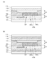
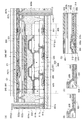
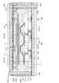
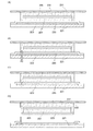
図4(A)は、本発明の一態様の入出力装置の断面図の一例である。図4(B)、(C)は、それぞれ発光素子の構成の一例である。図4(D)は、トランジスタFET1及び検知素子C1の拡大図である。
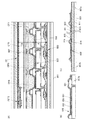
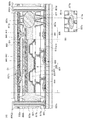
図5(A)は、本発明の一態様の入出力装置の断面図の一例である。図5(B)は、トランジスタFET2及び検知素子C2の拡大図である。
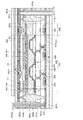
図7は、本発明の一態様の入出力装置の断面図の一例である。
図8は、本発明の一態様の入出力装置の断面図の一例である。
図9(A)は、本発明の一態様の入出力装置の断面図の一例である。
次に、入出力装置に用いることができる材料等を説明する。なお、本明細書中で先に説明した構成については説明を省略する場合がある。
本実施の形態では、本発明の一態様の入出力装置に用いることができる入力部について説明する。
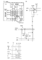
図10は入力部600の構成を説明する図である。図10(A)は入力部600の構成を説明するブロック図である。図10(B)は変換器CONV及び検知ユニット10Uの構成を説明する回路図である。図10(C−1)及び図10(C−2)は検知ユニット10Uの駆動方法を説明するタイミングチャートである。
検知ユニット10Uの駆動方法について説明する。
第1のステップにおいて、第3のトランジスタM3を導通状態にした後に非導通状態にするリセット信号をゲートに供給し、検知素子Cの第1の電極11の電位を所定の電位にする(図10(C−1)期間T1参照)。
第2のステップにおいて、第2のトランジスタM2を導通状態にする選択信号をゲートに供給し、第1のトランジスタM1の第2の電極を信号線DLに電気的に接続する。
第3のステップにおいて、制御信号を検知素子Cの第2の電極12に供給し、制御信号及び検知素子Cの容量に基づいて変化する電位を第1のトランジスタM1のゲートに供給する。
第4のステップにおいて、第1のトランジスタM1のゲートの電位の変化がもたらす信号を信号線DLに供給する。
第5のステップにおいて、第2のトランジスタM2を非導通状態にする選択信号をゲートに供給する。
図11は入力部600Bの構成を説明する図である。図11(A)は入力部600Bの構成を説明するブロック図である。図11(B)は変換器CONV及び検知ユニット10UBの構成を説明する回路図である。図11(C)は検知ユニット10UBの駆動方法を説明するタイミングチャートである。
第1のステップにおいて、第3のトランジスタM3を導通状態にした後に非導通状態にするリセット信号をゲートに供給し、検知素子Cの第1の電極11の電位を所定の電位にする(図11(C)期間T1参照)。
第2のステップにおいて、選択信号を検知素子Cの第2の電極12に供給し、選択信号及び検知素子Cの容量に基づいて変化する電位を第1のトランジスタM1のゲートに供給する(図11(C)期間T2参照)。
第3のステップにおいて、第1のトランジスタM1のゲートの電位の変化がもたらす信号を信号線DLに供給する。
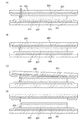
本実施の形態では、本発明の一態様の可撓性を有する入出力装置の作製方法を例示する。
本実施の形態では、本発明の一態様を適用して作製できる電子機器及び照明装置について、図16及び図17を用いて説明する。
10UB 検知ユニット
11 電極
12 電極
101 基板
102 接着層
103 絶縁層
105 トランジスタ
107 発光素子
107a 電極
107b EL層
107c 電極
109 接着層
111 素子層
113 絶縁層
114 接着層
115 基板
201 作製基板
203 剥離層
205 被剥離層
207 接着層
221 作製基板
223 剥離層
225 被剥離層
231 基板
233 接着層
304 ゲート電極
305 ゲート絶縁層
308a 半導体層
310 携帯情報端末
310a 電極
310b 電極
312 絶縁層
313 ヒンジ
314 絶縁層
315 筐体
316 表示パネル
320 携帯情報端末
322 表示部
325 非表示部
330 携帯情報端末
333 表示部
335 筐体
336 筐体
337 情報
339 操作ボタン
340 携帯情報端末
345 携帯情報端末
354 筐体
355 情報
356 情報
357 情報
358 表示部
375 絶縁層
500 表示部
500TP 入出力装置
502 画素
502B 副画素
502G 副画素
502R 副画素
502t トランジスタ
503c 容量
503g 走査線駆動回路
503s 信号線駆動回路
503t トランジスタ
511 配線
519 端子
521 絶縁膜
528 隔壁
550R 発光素子
580R 発光モジュール
600 入力部
600B 入力部
602 検知ユニット
603d 駆動回路
603g 駆動回路
650 容量素子
651 電極
652 電極
653 絶縁層
667 窓部
670 保護層
670p 反射防止層
801 基板
803 基板
804 発光部
806 駆動回路部
811 接着層
812 絶縁層
813 絶縁層
814 導電層
815 絶縁層
817 絶縁層
817a 絶縁層
817b 絶縁層
820 トランジスタ
821 絶縁層
822 接着層
822a 接着層
822b 接着層
823 スペーサ
825a 接続体
825b 接続体
830 発光素子
831 電極
832 光学調整層
833 EL層
835 電極
841 接着層
842 絶縁層
843 絶縁層
845 着色層
847 遮光層
851 オーバーコート
852 絶縁層
852a 絶縁層
852b 絶縁層
856 導電層
857a 導電層
857b 導電層
857c 導電層
857d 導電層
857e 導電層
877 導電性粒子
877a 導電性粒子
877b 樹脂層
7100 携帯情報端末
7101 筐体
7102 表示部
7103 バンド
7104 バックル
7105 操作ボタン
7106 入出力端子
7107 アイコン
7200 照明装置
7201 台部
7202 発光部
7203 操作スイッチ
7210 照明装置
7212 発光部
7220 照明装置
7222 発光部
7300 入出力装置
7301 筐体
7302 表示部
7303 操作ボタン
7304 部材
7305 制御部
7400 携帯電話機
7401 筐体
7402 表示部
7403 操作ボタン
7404 外部接続ポート
7405 スピーカ
7406 マイク
Claims (9)
- 可撓性を有する第1の基板と、
前記第1の基板上の、第1の絶縁層と、
前記第1の絶縁層上の、第1のトランジスタと、
前記第1のトランジスタ上の、発光素子と、
前記発光素子上の、第1の接着層と、
前記第1の接着層上の、検知素子及び第2のトランジスタと、
前記検知素子及び前記第2のトランジスタ上の、第2の絶縁層と、
前記第2の絶縁層上の、可撓性を有する第2の基板と、を有し、
前記発光素子は、第1の電極と、第2の電極と、前記第1の電極及び前記第2の電極の間の第1の層と、を有し、
前記第1の層は、発光性の有機化合物を有し、
前記発光素子は、前記第2の基板側に光を射出し、
前記第1のトランジスタ及び前記発光素子は、互いに電気的に接続し、
前記第2のトランジスタ及び前記検知素子は、互いに電気的に接続し、
前記発光性の有機化合物を含む層と前記第1の絶縁層の間の厚さをA、前記発光性の有機化合物を含む層と前記第2の絶縁層の間の厚さをBとしたとき、B/Aが0.7以上1.7以下である、入出力装置。 - 請求項1に記載の入出力装置は、厚さ1μm以上100μm以下である領域を有する、入出力装置。
- 請求項1又は2において、
前記第1の接着層は、厚さ50nm以上10μm以下である領域を有する、入出力装置。 - 請求項1乃至3のいずれか一項において、
前記第1の絶縁層上の第1の導電層を有し、
前記検知素子は、一対の電極と、前記一対の電極間の第3の絶縁層と、を有し、
前記一対の電極のいずれか一方と、前記第1の導電層と、が、導電性の接続体を介して互いに電気的に接続する、入出力装置。 - 請求項1乃至4のいずれか一項において、
前記第1の基板及び前記第1の絶縁層の間に、第2の接着層を有し、
前記第2の接着層は、厚さ50nm以上10μm以下である領域を有する、入出力装置。 - 請求項1乃至5のいずれか一項において、
前記第2の基板及び前記第2の絶縁層の間に、第3の接着層を有し、
前記第3の接着層は、厚さ50nm以上10μm以下である領域を有する、入出力装置。 - 請求項1乃至6のいずれか一項において、
前記第1の接着層を囲う、枠状の第4の接着層を有する、入出力装置。 - 請求項1乃至7のいずれか一項において、
前記第2の接着層の端部の少なくとも一部は、前記第1の基板の端部よりも外側に位置する、入出力装置。 - 請求項1乃至8のいずれか一項において、
前記第3の接着層の端部の少なくとも一部は、前記第2の基板の端部よりも外側に位置する、入出力装置。
Priority Applications (1)
| Application Number | Priority Date | Filing Date | Title |
|---|---|---|---|
| JP2015090088A JP2015228367A (ja) | 2014-05-02 | 2015-04-27 | 半導体装置、入出力装置、及び電子機器 |
Applications Claiming Priority (3)
| Application Number | Priority Date | Filing Date | Title |
|---|---|---|---|
| JP2014095116 | 2014-05-02 | ||
| JP2014095116 | 2014-05-02 | ||
| JP2015090088A JP2015228367A (ja) | 2014-05-02 | 2015-04-27 | 半導体装置、入出力装置、及び電子機器 |
Related Child Applications (1)
| Application Number | Title | Priority Date | Filing Date |
|---|---|---|---|
| JP2020079130A Division JP2020160452A (ja) | 2014-05-02 | 2020-04-28 | 入出力装置 |
Publications (2)
| Publication Number | Publication Date |
|---|---|
| JP2015228367A true JP2015228367A (ja) | 2015-12-17 |
| JP2015228367A5 JP2015228367A5 (ja) | 2018-05-31 |
Family
ID=54355233
Family Applications (3)
| Application Number | Title | Priority Date | Filing Date |
|---|---|---|---|
| JP2015090088A Withdrawn JP2015228367A (ja) | 2014-05-02 | 2015-04-27 | 半導体装置、入出力装置、及び電子機器 |
| JP2020079130A Withdrawn JP2020160452A (ja) | 2014-05-02 | 2020-04-28 | 入出力装置 |
| JP2021145143A Withdrawn JP2022008335A (ja) | 2014-05-02 | 2021-09-07 | 入出力装置 |
Family Applications After (2)
| Application Number | Title | Priority Date | Filing Date |
|---|---|---|---|
| JP2020079130A Withdrawn JP2020160452A (ja) | 2014-05-02 | 2020-04-28 | 入出力装置 |
| JP2021145143A Withdrawn JP2022008335A (ja) | 2014-05-02 | 2021-09-07 | 入出力装置 |
Country Status (2)
| Country | Link |
|---|---|
| US (3) | US9865665B2 (ja) |
| JP (3) | JP2015228367A (ja) |
Cited By (6)
| Publication number | Priority date | Publication date | Assignee | Title |
|---|---|---|---|---|
| WO2017135227A1 (ja) * | 2016-02-01 | 2017-08-10 | シャープ株式会社 | 有機el表示装置 |
| WO2017138416A1 (ja) * | 2016-02-08 | 2017-08-17 | シャープ株式会社 | 有機el表示装置 |
| JP2018110223A (ja) * | 2016-12-28 | 2018-07-12 | 株式会社半導体エネルギー研究所 | 発光素子、有機化合物、発光装置、電子機器、及び照明装置 |
| CN110114712A (zh) * | 2017-01-06 | 2019-08-09 | 夏普株式会社 | 弯曲显示面板 |
| JPWO2019135147A1 (ja) * | 2018-01-05 | 2021-01-07 | 株式会社半導体エネルギー研究所 | 表示装置、表示モジュール、及び電子機器 |
| WO2023067437A1 (ja) * | 2021-10-22 | 2023-04-27 | 株式会社半導体エネルギー研究所 | 表示装置 |
Families Citing this family (22)
| Publication number | Priority date | Publication date | Assignee | Title |
|---|---|---|---|---|
| CN105144841B (zh) | 2013-04-15 | 2017-11-17 | 株式会社半导体能源研究所 | 发光装置 |
| JP6518133B2 (ja) | 2014-05-30 | 2019-05-22 | 株式会社半導体エネルギー研究所 | 入力装置 |
| US9455281B2 (en) | 2014-06-19 | 2016-09-27 | Semiconductor Energy Laboratory Co., Ltd. | Touch sensor, touch panel, touch panel module, and display device |
| KR20180012285A (ko) | 2015-05-28 | 2018-02-05 | 가부시키가이샤 한도오따이 에네루기 켄큐쇼 | 터치 패널 |
| US10510989B2 (en) * | 2015-07-10 | 2019-12-17 | Sharp Kabushiki Kaisha | Electroluminescent device |
| US10978489B2 (en) * | 2015-07-24 | 2021-04-13 | Semiconductor Energy Laboratory Co., Ltd. | Semiconductor device, display panel, method for manufacturing semiconductor device, method for manufacturing display panel, and information processing device |
| ITUB20152606A1 (it) * | 2015-07-29 | 2017-01-29 | Industria Lombarda Mat Elettrico I L M E S P A | Custodia di connettore protetta contro la corrosione e l’erosione |
| US10304813B2 (en) * | 2015-11-05 | 2019-05-28 | Innolux Corporation | Display device having a plurality of bank structures |
| KR101730537B1 (ko) * | 2015-11-30 | 2017-04-26 | 엘지디스플레이 주식회사 | 표시장치와 그의 제조방법 |
| US10558265B2 (en) | 2015-12-11 | 2020-02-11 | Semiconductor Energy Laboratory Co., Ltd. | Input device and system of input device |
| US10229316B2 (en) * | 2016-01-29 | 2019-03-12 | Synaptics Incorporated | Compound collimating system using apertures and collimators |
| WO2017214971A1 (en) * | 2016-06-17 | 2017-12-21 | Boe Technology Group Co., Ltd. | Touch display substrate, touch display apparatus having the same, pixel arrangement, and fabricating method thereof |
| JP2018063669A (ja) * | 2016-10-14 | 2018-04-19 | 株式会社ジャパンディスプレイ | 表示装置 |
| CN110121675B (zh) * | 2017-01-06 | 2022-02-11 | 夏普株式会社 | 弯曲显示面板 |
| US12446455B2 (en) * | 2017-02-21 | 2025-10-14 | Beijing Boe Technology Co., Ltd. | Flexible display panel |
| JP7293190B2 (ja) | 2018-03-16 | 2023-06-19 | 株式会社半導体エネルギー研究所 | 半導体装置 |
| TWI681554B (zh) * | 2018-05-10 | 2020-01-01 | 友達光電股份有限公司 | 畫素陣列基板及其驅動方法 |
| US12253391B2 (en) | 2018-05-24 | 2025-03-18 | The Research Foundation For The State University Of New York | Multielectrode capacitive sensor without pull-in risk |
| JP7373124B2 (ja) * | 2019-01-25 | 2023-11-02 | 大日本印刷株式会社 | 調光装置及びその製造方法 |
| TWI710820B (zh) * | 2019-03-28 | 2020-11-21 | 友達光電股份有限公司 | 顯示裝置 |
| CN110098199B (zh) * | 2019-05-05 | 2022-04-05 | 深圳市华星光电半导体显示技术有限公司 | 显示面板及显示装置 |
| KR20220141386A (ko) | 2021-04-12 | 2022-10-20 | 삼성디스플레이 주식회사 | 표시 장치 |
Citations (5)
| Publication number | Priority date | Publication date | Assignee | Title |
|---|---|---|---|---|
| JP2003196023A (ja) * | 2001-12-27 | 2003-07-11 | Sony Corp | 表示装置 |
| JP2012518892A (ja) * | 2009-02-25 | 2012-08-16 | グローバル・オーエルイーディー・テクノロジー・リミテッド・ライアビリティ・カンパニー | チップレットを備えるフレキシブルoledディスプレイ |
| US20130299789A1 (en) * | 2012-05-09 | 2013-11-14 | Semiconductor Energy Laboratory Co., Ltd. | Light-Emitting Device and Electronic Device |
| JP2014029853A (ja) * | 2012-07-05 | 2014-02-13 | Semiconductor Energy Lab Co Ltd | 発光装置及び発光装置の作製方法 |
| JP2014032960A (ja) * | 2012-07-12 | 2014-02-20 | Semiconductor Energy Lab Co Ltd | 表示装置、及び表示装置の作製方法 |
Family Cites Families (25)
| Publication number | Priority date | Publication date | Assignee | Title |
|---|---|---|---|---|
| US7663607B2 (en) | 2004-05-06 | 2010-02-16 | Apple Inc. | Multipoint touchscreen |
| US8415208B2 (en) | 2001-07-16 | 2013-04-09 | Semiconductor Energy Laboratory Co., Ltd. | Semiconductor device and peeling off method and method of manufacturing semiconductor device |
| JP4027740B2 (ja) | 2001-07-16 | 2007-12-26 | 株式会社半導体エネルギー研究所 | 半導体装置の作製方法 |
| US6751552B1 (en) * | 2002-06-28 | 2004-06-15 | Garmin Ltd. | Rugged, waterproof, navigation device with touch panel |
| AU2003262039A1 (en) * | 2003-09-10 | 2005-04-06 | Fujitsu Limited | Display and process for manufacturing the same |
| EP1528594B1 (en) * | 2003-10-28 | 2019-05-29 | Semiconductor Energy Laboratory Co., Ltd. | Method for manufacturing semiconductor device |
| US20050200292A1 (en) | 2004-02-24 | 2005-09-15 | Naugler W. E.Jr. | Emissive display device having sensing for luminance stabilization and user light or touch screen input |
| US20060013246A1 (en) * | 2004-07-13 | 2006-01-19 | International Business Machines Corporation | System, apparatus and method for gigabit ethernet communications over an IBM cabling system |
| US7825582B2 (en) * | 2004-11-08 | 2010-11-02 | Kyodo Printing Co., Ltd. | Flexible display and manufacturing method thereof |
| US8013943B2 (en) | 2006-03-08 | 2011-09-06 | Sharp Kabushiki Kaisha | Display device |
| US8243027B2 (en) | 2006-06-09 | 2012-08-14 | Apple Inc. | Touch screen liquid crystal display |
| JP4957597B2 (ja) | 2007-05-18 | 2012-06-20 | セイコーエプソン株式会社 | センシング回路、その駆動方法、表示装置および電子機器 |
| TWI350474B (en) | 2007-09-29 | 2011-10-11 | Au Optronics Corp | Capacitive touch panel with low impedance and method of manufacturing capacitive touch panels with low impedance |
| US20130029978A1 (en) * | 2009-12-25 | 2013-01-31 | Mochida Pharmaceutical Co., Ltd. | Novel aryl urea derivative |
| JP5789113B2 (ja) * | 2011-03-31 | 2015-10-07 | 株式会社Joled | 表示装置および電子機器 |
| JP2013251255A (ja) | 2012-05-04 | 2013-12-12 | Semiconductor Energy Lab Co Ltd | 発光装置の作製方法 |
| KR101963810B1 (ko) * | 2012-08-22 | 2019-04-02 | 삼성디스플레이 주식회사 | 유기 발광 디스플레이 장치 |
| KR102161078B1 (ko) | 2012-08-28 | 2020-09-29 | 가부시키가이샤 한도오따이 에네루기 켄큐쇼 | 표시 장치 및 그 제작 방법 |
| US11074025B2 (en) * | 2012-09-03 | 2021-07-27 | Semiconductor Energy Laboratory Co., Ltd. | Display device and method for manufacturing the same |
| JP5810121B2 (ja) * | 2013-03-29 | 2015-11-11 | 株式会社ジャパンディスプレイ | 電子機器および電子機器の制御方法 |
| KR102239367B1 (ko) | 2013-11-27 | 2021-04-09 | 가부시키가이샤 한도오따이 에네루기 켄큐쇼 | 터치 패널 |
| DE112015000739T5 (de) | 2014-02-11 | 2016-12-29 | Semiconductor Energy Laboratory Co., Ltd. | Anzeigevorrichtung und elektronisches Gerät |
| WO2015132694A1 (en) | 2014-03-07 | 2015-09-11 | Semiconductor Energy Laboratory Co., Ltd. | Touch sensor, touch panel, and manufacturing method of touch panel |
| JP2015187852A (ja) | 2014-03-13 | 2015-10-29 | 株式会社半導体エネルギー研究所 | タッチパネル |
| JP6613044B2 (ja) | 2014-04-22 | 2019-11-27 | 株式会社半導体エネルギー研究所 | 表示装置、表示モジュール、及び電子機器 |
-
2015
- 2015-04-27 JP JP2015090088A patent/JP2015228367A/ja not_active Withdrawn
- 2015-04-30 US US14/700,527 patent/US9865665B2/en active Active
-
2018
- 2018-01-04 US US15/861,945 patent/US10622426B2/en active Active
-
2020
- 2020-04-10 US US16/845,517 patent/US11171190B2/en active Active
- 2020-04-28 JP JP2020079130A patent/JP2020160452A/ja not_active Withdrawn
-
2021
- 2021-09-07 JP JP2021145143A patent/JP2022008335A/ja not_active Withdrawn
Patent Citations (5)
| Publication number | Priority date | Publication date | Assignee | Title |
|---|---|---|---|---|
| JP2003196023A (ja) * | 2001-12-27 | 2003-07-11 | Sony Corp | 表示装置 |
| JP2012518892A (ja) * | 2009-02-25 | 2012-08-16 | グローバル・オーエルイーディー・テクノロジー・リミテッド・ライアビリティ・カンパニー | チップレットを備えるフレキシブルoledディスプレイ |
| US20130299789A1 (en) * | 2012-05-09 | 2013-11-14 | Semiconductor Energy Laboratory Co., Ltd. | Light-Emitting Device and Electronic Device |
| JP2014029853A (ja) * | 2012-07-05 | 2014-02-13 | Semiconductor Energy Lab Co Ltd | 発光装置及び発光装置の作製方法 |
| JP2014032960A (ja) * | 2012-07-12 | 2014-02-20 | Semiconductor Energy Lab Co Ltd | 表示装置、及び表示装置の作製方法 |
Cited By (12)
| Publication number | Priority date | Publication date | Assignee | Title |
|---|---|---|---|---|
| WO2017135227A1 (ja) * | 2016-02-01 | 2017-08-10 | シャープ株式会社 | 有機el表示装置 |
| WO2017138416A1 (ja) * | 2016-02-08 | 2017-08-17 | シャープ株式会社 | 有機el表示装置 |
| JP2018110223A (ja) * | 2016-12-28 | 2018-07-12 | 株式会社半導体エネルギー研究所 | 発光素子、有機化合物、発光装置、電子機器、及び照明装置 |
| JP7120759B2 (ja) | 2016-12-28 | 2022-08-17 | 株式会社半導体エネルギー研究所 | 発光素子、有機化合物、表示装置、電子機器、及び照明装置 |
| US12102000B2 (en) | 2016-12-28 | 2024-09-24 | Semiconductor Energy Laboratory Co., Ltd. | Light-emitting element, organic compound, light-emitting device, electronic device, and lighting device |
| CN110114712A (zh) * | 2017-01-06 | 2019-08-09 | 夏普株式会社 | 弯曲显示面板 |
| CN110114712B (zh) * | 2017-01-06 | 2021-12-21 | 夏普株式会社 | 弯曲显示面板 |
| JPWO2019135147A1 (ja) * | 2018-01-05 | 2021-01-07 | 株式会社半導体エネルギー研究所 | 表示装置、表示モジュール、及び電子機器 |
| JP7242558B2 (ja) | 2018-01-05 | 2023-03-20 | 株式会社半導体エネルギー研究所 | 表示モジュール |
| US11733574B2 (en) | 2018-01-05 | 2023-08-22 | Semiconductor Energy Laboratory Co., Ltd. | Display device, display module, and electronic device |
| US11940703B2 (en) | 2018-01-05 | 2024-03-26 | Semiconductor Energy Laboratory Co., Ltd. | Display device, display module, and electronic device |
| WO2023067437A1 (ja) * | 2021-10-22 | 2023-04-27 | 株式会社半導体エネルギー研究所 | 表示装置 |
Also Published As
| Publication number | Publication date |
|---|---|
| US10622426B2 (en) | 2020-04-14 |
| US20150317015A1 (en) | 2015-11-05 |
| US11171190B2 (en) | 2021-11-09 |
| US9865665B2 (en) | 2018-01-09 |
| US20180130861A1 (en) | 2018-05-10 |
| JP2020160452A (ja) | 2020-10-01 |
| US20200243626A1 (en) | 2020-07-30 |
| JP2022008335A (ja) | 2022-01-13 |
Similar Documents
| Publication | Publication Date | Title |
|---|---|---|
| US11171190B2 (en) | Semiconductor device, input/output device, and electronic appliance | |
| JP6915012B2 (ja) | 入出力装置 | |
| JP7128319B2 (ja) | タッチパネル | |
| JP2024026129A (ja) | 発光装置 | |
| JP6942167B2 (ja) | 電子機器 | |
| JP2022058677A (ja) | 表示装置および表示装置の画像処理方法 | |
| CN111443833B (zh) | 触摸面板 | |
| JP6517617B2 (ja) | 表示装置 | |
| US9960213B2 (en) | Input and output device having touch sensor element as input device and display device | |
| JP6727762B2 (ja) | 発光装置及び電子機器 | |
| JP2025123402A (ja) | 発光装置 | |
| CN106663396B (zh) | 显示装置 | |
| JP6346782B2 (ja) | タッチパネル |
Legal Events
| Date | Code | Title | Description |
|---|---|---|---|
| A521 | Request for written amendment filed |
Free format text: JAPANESE INTERMEDIATE CODE: A523 Effective date: 20180406 |
|
| A621 | Written request for application examination |
Free format text: JAPANESE INTERMEDIATE CODE: A621 Effective date: 20180406 |
|
| A977 | Report on retrieval |
Free format text: JAPANESE INTERMEDIATE CODE: A971007 Effective date: 20190115 |
|
| A131 | Notification of reasons for refusal |
Free format text: JAPANESE INTERMEDIATE CODE: A131 Effective date: 20190226 |
|
| A521 | Request for written amendment filed |
Free format text: JAPANESE INTERMEDIATE CODE: A523 Effective date: 20190426 |
|
| A131 | Notification of reasons for refusal |
Free format text: JAPANESE INTERMEDIATE CODE: A131 Effective date: 20190910 |
|
| A601 | Written request for extension of time |
Free format text: JAPANESE INTERMEDIATE CODE: A601 Effective date: 20191107 |
|
| A02 | Decision of refusal |
Free format text: JAPANESE INTERMEDIATE CODE: A02 Effective date: 20200128 |
|
| A761 | Written withdrawal of application |
Free format text: JAPANESE INTERMEDIATE CODE: A761 Effective date: 20200428 |