JP2015509257A - パラレルメモリテストを実行するためのデバイスおよび方法 - Google Patents
パラレルメモリテストを実行するためのデバイスおよび方法 Download PDFInfo
- Publication number
- JP2015509257A JP2015509257A JP2014555102A JP2014555102A JP2015509257A JP 2015509257 A JP2015509257 A JP 2015509257A JP 2014555102 A JP2014555102 A JP 2014555102A JP 2014555102 A JP2014555102 A JP 2014555102A JP 2015509257 A JP2015509257 A JP 2015509257A
- Authority
- JP
- Japan
- Prior art keywords
- module
- modules
- mem
- memory
- output data
- Prior art date
- Legal status (The legal status is an assumption and is not a legal conclusion. Google has not performed a legal analysis and makes no representation as to the accuracy of the status listed.)
- Pending
Links
Images




Classifications
-
- G—PHYSICS
- G11—INFORMATION STORAGE
- G11C—STATIC STORES
- G11C29/00—Checking stores for correct operation ; Subsequent repair; Testing stores during standby or offline operation
- G11C29/04—Detection or location of defective memory elements, e.g. cell constructio details, timing of test signals
-
- G—PHYSICS
- G11—INFORMATION STORAGE
- G11C—STATIC STORES
- G11C29/00—Checking stores for correct operation ; Subsequent repair; Testing stores during standby or offline operation
- G11C29/04—Detection or location of defective memory elements, e.g. cell constructio details, timing of test signals
- G11C29/08—Functional testing, e.g. testing during refresh, power-on self testing [POST] or distributed testing
- G11C29/12—Built-in arrangements for testing, e.g. built-in self testing [BIST] or interconnection details
-
- G—PHYSICS
- G11—INFORMATION STORAGE
- G11C—STATIC STORES
- G11C29/00—Checking stores for correct operation ; Subsequent repair; Testing stores during standby or offline operation
- G11C29/04—Detection or location of defective memory elements, e.g. cell constructio details, timing of test signals
- G11C29/08—Functional testing, e.g. testing during refresh, power-on self testing [POST] or distributed testing
- G11C29/12—Built-in arrangements for testing, e.g. built-in self testing [BIST] or interconnection details
- G11C29/14—Implementation of control logic, e.g. test mode decoders
-
- G—PHYSICS
- G11—INFORMATION STORAGE
- G11C—STATIC STORES
- G11C29/00—Checking stores for correct operation ; Subsequent repair; Testing stores during standby or offline operation
- G11C29/04—Detection or location of defective memory elements, e.g. cell constructio details, timing of test signals
- G11C29/08—Functional testing, e.g. testing during refresh, power-on self testing [POST] or distributed testing
- G11C29/12—Built-in arrangements for testing, e.g. built-in self testing [BIST] or interconnection details
- G11C29/18—Address generation devices; Devices for accessing memories, e.g. details of addressing circuits
- G11C29/26—Accessing multiple arrays
-
- G—PHYSICS
- G11—INFORMATION STORAGE
- G11C—STATIC STORES
- G11C29/00—Checking stores for correct operation ; Subsequent repair; Testing stores during standby or offline operation
- G11C29/04—Detection or location of defective memory elements, e.g. cell constructio details, timing of test signals
- G11C29/08—Functional testing, e.g. testing during refresh, power-on self testing [POST] or distributed testing
- G11C29/48—Arrangements in static stores specially adapted for testing by means external to the store, e.g. using direct memory access [DMA] or using auxiliary access paths
-
- G—PHYSICS
- G11—INFORMATION STORAGE
- G11C—STATIC STORES
- G11C29/00—Checking stores for correct operation ; Subsequent repair; Testing stores during standby or offline operation
- G11C29/04—Detection or location of defective memory elements, e.g. cell constructio details, timing of test signals
- G11C29/50—Marginal testing, e.g. race, voltage or current testing
-
- G—PHYSICS
- G11—INFORMATION STORAGE
- G11C—STATIC STORES
- G11C29/00—Checking stores for correct operation ; Subsequent repair; Testing stores during standby or offline operation
- G11C29/04—Detection or location of defective memory elements, e.g. cell constructio details, timing of test signals
- G11C29/08—Functional testing, e.g. testing during refresh, power-on self testing [POST] or distributed testing
- G11C29/12—Built-in arrangements for testing, e.g. built-in self testing [BIST] or interconnection details
- G11C29/18—Address generation devices; Devices for accessing memories, e.g. details of addressing circuits
- G11C29/26—Accessing multiple arrays
- G11C2029/2602—Concurrent test
Abstract
Description
通常、複数のメモリモジュールのパラレルテストは同じサイズのモジュールに限定されている。それでもなお、半導体デバイスは、たとえば、半導体基板上の集積回路の大型メモリのレイアウトを最適化するために、異なるサイズのモジュールを備えうる。
例1:システムアドレスSA=700、パラレル信号PS=0。信号SL0'は1に設定され、信号SL1'、SL2'は0に設定される。
例2:システムアドレスSA=500、パラレル信号PS=1。信号SL0'、SL1'は1に設定されて、信号SL2'は0に設定される。
例3:システムアドレスSA=200、パラレル信号PS=1。信号SL0'、SL1'、SL2'は1に設定される。
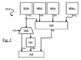
ATE 自動試験装置
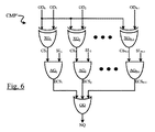
CMP 出力データ比較器回路
CP 比較器
DB データバス
DMX デマルチプレクサ
DV1 半導体デバイス
DV2 半導体デバイス
MEM メモリモジュール
MDEC モジュール復号器
RCT 読取り回路
WCT 書込み回路
Claims (9)
- - 各モジュールが行および列に配列されたメモリセルアレイを備えたN個のメモリモジュール(MEM0-MEMN-1、MEM0'-MEM2')、ただしNは3以上と、
- 前記各モジュールに結合され、前記メモリセル内にデータ(ID)を書き込むように構成された書込み回路(WCT)と、
- 前記各モジュールに結合され、前記メモリセルから出力データ(OD0-ODN-1)を提供するように構成された読取り回路(RCT)と
- 通常の動作モードでは1個のメモリモジュール(MEM0-MEMN-1、MEM0'-MEM2')を個々に選択して、パラレルモードでは前記モジュールの2つ以上を一括選択するように構成されたモジュール選択回路(MDEC)と、
- 前記N個のモジュールに結合され、前記パラレルモードでは、前記N個のモジュールのうちの少なくとも2つによって提供された前記出力データを比較するように構成された比較器回路(CMP、CMP')と
を備え、
- 前記N個のメモリモジュールが、基準モジュールとして指定された1個のモジュール(MEM0、MEM0')と、補助モジュールとして指定されたN-1個のモジュール(MEM1-MEMN-1、MEM1'、MEM2)とを備え、
- 前記比較器回路(CMP、CMP')が、各補助モジュールによって提供された前記出力データ(OD1-ODN-1)を前記基準モジュールによって提供された前記出力データ(OD0)と比較するように構成され、
- 前記出力データ(OD0)を前記基準モジュール(MEM0、MEM0')からデータ検証手段(ATE)に提供するように構成される
ことを特徴とする、半導体デバイス(DV1、DV2)。 - 前記基準モジュール(MEM0、MEM0')によって提供された前記出力データ(OD0)に関する巡回冗長検査を実行して、検査結果(CRR)を前記データ検証手段(ATE)に提供するように構成された回路(CRC)をさらに備える、請求項1に記載のデバイス。
- 前記検証手段(ATE)が、前記モジュール選択回路(MDEC)と、前記比較器回路(CMP、CMP')と、前記基準モジュール(MEM0、MEM0')とに結合された内蔵セルフテスト回路である、請求項1または2のいずれか一項に記載のデバイス。
- 前記比較器回路(CMP')が、モジュール選択信号(SL1-SLN-1、SL1'、SL2')の状態に応じて、補助モジュール(MEM1-MEMN-1、MEM1'、MEM2')によって提供された出力データ(OD1-ODN-1)と前記基準モジュール(MEM0、MEM0')によって提供された前記出力データ(OD0)との比較を有効および無効にするための手段(AG1-AGN-1)をさらに備える、請求項1から3のいずれか一項に記載のデバイス。
- 前記メモリモジュール(MEM0'、MEM1'、MEM2')のうちの少なくとも2つはメモリセルの行数が異なり、行数が最大の前記メモリモジュール(MEM0')が基準アレイとして指定される、請求項1から4のいずれか一項に記載のデバイス。
- 前記モジュール選択回路(MDEC)が、
- 入力部においてパラレル信号(PS)とモジュール信号(MS)とを受信して、
- 出力部からN個のモジュール選択信号(SL0-SLN-1、SL0'-SL2')をモジュールごとに1個提供して、
- 前記パラレル信号の状態にかかわらず、1つまたは複数の選択信号を非選択状態にするように構成された、請求項5に記載のデバイス。 - N個のメモリモジュール(MEM0-MEMN-1、MEM0'-MEM2')、ただしNは3以上、に対してパラレルテストを実行する方法であって、
- 前記メモリモジュールの各々内でアドレス(AD)に入力データ(ID)を書き込むステップと、
- 出力データ(OD0-ODN-1)を取得するために、前記モジュールの前記アドレスにおける前記データを読み取るステップと、
- 前記モジュールからの前記出力データが同一(EQ、NQ)かどうかを判定するステップと
を含み、
- 前記モジュールのうちの1つを基準モジュール(MEM0、MEM0')として指定して、N-1個の他のモジュール(MEM1-MEMN-1、MEM1'、MEM2')を補助モジュールとして指定するステップと、
- テストされている前記補助モジュールの各々からの前記出力データ(OD1-ODN-1)を前記基準モジュールからの前記出力データ(OD0)と比較するステップと、
- 前記出力データを前記基準モジュールからデータ検証手段(ATE)に提供するステップと
をさらに含むことを特徴とする、方法。 - - 最大のメモリモジュール(MEM0')を決定するステップと、
- 前記最大のメモリモジュールを前記基準モジュールとして指定するステップと
を含む、請求項7に記載の方法。 - パラレル動作の間、前記N個のメモリモジュールのうち少なくとも2つのメモリモジュールのサブセット(MEM0'、MEM1')に共通しているテスト空間(TS012、TS01)に属しているアドレスに従って、前記少なくとも2つのモジュールの前記サブセットを選択するステップをさらに含む、請求項8に記載の方法。
Applications Claiming Priority (3)
| Application Number | Priority Date | Filing Date | Title |
|---|---|---|---|
| GB1201755.4A GB2498980A (en) | 2012-02-01 | 2012-02-01 | Device and method to perform a parallel memory test |
| GB1201755.4 | 2012-02-01 | ||
| PCT/EP2012/073966 WO2013113426A1 (en) | 2012-02-01 | 2012-11-29 | Device and method to perform a parallel memory test |
Publications (1)
| Publication Number | Publication Date |
|---|---|
| JP2015509257A true JP2015509257A (ja) | 2015-03-26 |
Family
ID=45876481
Family Applications (1)
| Application Number | Title | Priority Date | Filing Date |
|---|---|---|---|
| JP2014555102A Pending JP2015509257A (ja) | 2012-02-01 | 2012-11-29 | パラレルメモリテストを実行するためのデバイスおよび方法 |
Country Status (7)
| Country | Link |
|---|---|
| US (1) | US9202594B2 (ja) |
| EP (1) | EP2810281B1 (ja) |
| JP (1) | JP2015509257A (ja) |
| KR (1) | KR20140117516A (ja) |
| CN (1) | CN104094357B (ja) |
| GB (1) | GB2498980A (ja) |
| WO (1) | WO2013113426A1 (ja) |
Families Citing this family (7)
| Publication number | Priority date | Publication date | Assignee | Title |
|---|---|---|---|---|
| CN105302688B (zh) * | 2015-09-18 | 2018-03-16 | 许继集团有限公司 | 一种并行总线自检方法及系统 |
| US20170125125A1 (en) * | 2015-10-30 | 2017-05-04 | Texas Instruments Incorporated | Area-efficient parallel test data path for embedded memories |
| CN106370992A (zh) * | 2016-08-17 | 2017-02-01 | 上海华岭集成电路技术股份有限公司 | 用于半导体芯片测试的 uid 写入系统及方法 |
| US10157151B2 (en) * | 2016-10-19 | 2018-12-18 | Stmicroelectronics S.R.L. | System and method of determining memory access time |
| US10528288B2 (en) * | 2017-12-20 | 2020-01-07 | International Business Machines Corporation | Three-dimensional stacked memory access optimization |
| US12014788B2 (en) | 2022-04-29 | 2024-06-18 | Changxin Memory Technologies, Inc. | Memory array detection circuit and detection method, and memory |
| CN117012256A (zh) * | 2022-04-29 | 2023-11-07 | 长鑫存储技术有限公司 | 一种存储阵列的检测电路及其检测方法、存储器 |
Citations (7)
| Publication number | Priority date | Publication date | Assignee | Title |
|---|---|---|---|---|
| US5982684A (en) * | 1998-05-28 | 1999-11-09 | Intel Corporation | Parallel access testing of a memory array |
| JP2000322329A (ja) * | 1999-05-11 | 2000-11-24 | Mitsubishi Electric Corp | 半導体集積回路装置 |
| JP2001135096A (ja) * | 1999-11-02 | 2001-05-18 | Kawasaki Steel Corp | Ramのテスト方法 |
| US20040125667A1 (en) * | 2002-08-05 | 2004-07-01 | Hiroyuki Sadakata | Semiconductor memory device and method for testing the same |
| JP2004234741A (ja) * | 2003-01-29 | 2004-08-19 | Nec Electronics Corp | テスト回路及び半導体装置 |
| US20050216808A1 (en) * | 2004-03-05 | 2005-09-29 | Peter Poechmueller | Method and circuit arrangement for testing electrical modules |
| JP2008269692A (ja) * | 2007-04-19 | 2008-11-06 | Matsushita Electric Ind Co Ltd | 半導体装置およびその検査方法 |
Family Cites Families (12)
| Publication number | Priority date | Publication date | Assignee | Title |
|---|---|---|---|---|
| JP2780354B2 (ja) * | 1989-07-04 | 1998-07-30 | 富士通株式会社 | 半導体メモリ装置 |
| US6357027B1 (en) * | 1999-05-17 | 2002-03-12 | Infineon Technologies Ag | On chip data comparator with variable data and compare result compression |
| JP4495308B2 (ja) * | 2000-06-14 | 2010-07-07 | 株式会社アドバンテスト | 半導体デバイス試験方法・半導体デバイス試験装置 |
| DE10124923B4 (de) * | 2001-05-21 | 2014-02-06 | Qimonda Ag | Testverfahren zum Testen eines Datenspeichers und Datenspeicher mit integrierter Testdatenkompressionsschaltung |
| EP1369878A1 (en) * | 2002-06-04 | 2003-12-10 | Infineon Technologies AG | System for testing a group of functionally independent memories and for replacing failing memory words |
| US7392442B2 (en) * | 2003-03-20 | 2008-06-24 | Qualcomm Incorporated | Built-in self-test (BIST) architecture having distributed interpretation and generalized command protocol |
| JP4051008B2 (ja) * | 2003-07-15 | 2008-02-20 | 松下電器産業株式会社 | 半導体装置 |
| KR100624576B1 (ko) * | 2004-06-11 | 2006-09-19 | 삼성전자주식회사 | 허브를 갖는 메모리 모듈을 테스트하는 방법 및 이를수행하기 위한 메모리 모듈의 허브 |
| JP2006120241A (ja) * | 2004-10-21 | 2006-05-11 | Toshiba Corp | 半導体装置 |
| US7152192B2 (en) * | 2005-01-20 | 2006-12-19 | Hewlett-Packard Development Company, L.P. | System and method of testing a plurality of memory blocks of an integrated circuit in parallel |
| JP2008159168A (ja) * | 2006-12-25 | 2008-07-10 | Elpida Memory Inc | 半導体記憶装置 |
| KR100885912B1 (ko) * | 2007-01-23 | 2009-02-26 | 삼성전자주식회사 | 기입된 데이터 값에 기초하여 데이터를 선택적으로검증하는 데이터 검증 방법 및 반도체 메모리 장치 |
-
2012
- 2012-02-01 GB GB1201755.4A patent/GB2498980A/en not_active Withdrawn
- 2012-11-29 EP EP12805627.2A patent/EP2810281B1/en active Active
- 2012-11-29 WO PCT/EP2012/073966 patent/WO2013113426A1/en not_active Ceased
- 2012-11-29 US US14/376,263 patent/US9202594B2/en not_active Expired - Fee Related
- 2012-11-29 JP JP2014555102A patent/JP2015509257A/ja active Pending
- 2012-11-29 KR KR1020147022269A patent/KR20140117516A/ko not_active Withdrawn
- 2012-11-29 CN CN201280068807.8A patent/CN104094357B/zh not_active Expired - Fee Related
Patent Citations (8)
| Publication number | Priority date | Publication date | Assignee | Title |
|---|---|---|---|---|
| US5982684A (en) * | 1998-05-28 | 1999-11-09 | Intel Corporation | Parallel access testing of a memory array |
| JP2000322329A (ja) * | 1999-05-11 | 2000-11-24 | Mitsubishi Electric Corp | 半導体集積回路装置 |
| JP2001135096A (ja) * | 1999-11-02 | 2001-05-18 | Kawasaki Steel Corp | Ramのテスト方法 |
| US20040125667A1 (en) * | 2002-08-05 | 2004-07-01 | Hiroyuki Sadakata | Semiconductor memory device and method for testing the same |
| JP2004234741A (ja) * | 2003-01-29 | 2004-08-19 | Nec Electronics Corp | テスト回路及び半導体装置 |
| US20050114063A1 (en) * | 2003-01-29 | 2005-05-26 | Nec Electronics Corporation | Semiconductor device and testing circuit which can carries out a verifying test effectively for non-volatile memory cells |
| US20050216808A1 (en) * | 2004-03-05 | 2005-09-29 | Peter Poechmueller | Method and circuit arrangement for testing electrical modules |
| JP2008269692A (ja) * | 2007-04-19 | 2008-11-06 | Matsushita Electric Ind Co Ltd | 半導体装置およびその検査方法 |
Also Published As
| Publication number | Publication date |
|---|---|
| EP2810281B1 (en) | 2019-03-20 |
| KR20140117516A (ko) | 2014-10-07 |
| EP2810281A1 (en) | 2014-12-10 |
| US20150063045A1 (en) | 2015-03-05 |
| GB201201755D0 (en) | 2012-03-14 |
| GB2498980A (en) | 2013-08-07 |
| US9202594B2 (en) | 2015-12-01 |
| WO2013113426A1 (en) | 2013-08-08 |
| CN104094357A (zh) | 2014-10-08 |
| CN104094357B (zh) | 2017-03-29 |
Similar Documents
| Publication | Publication Date | Title |
|---|---|---|
| CN105745623B (zh) | 集成电路缺陷检测和修复 | |
| CN104094357B (zh) | 执行并行存储测试的装置和方法 | |
| US8201037B2 (en) | Semiconductor integrated circuit and method for controlling semiconductor integrated circuit | |
| EP1388150B1 (en) | Integrated circuit with self-test device for an embedded non-volatile memory and related test method | |
| CN103021467B (zh) | 故障诊断电路 | |
| US9564245B2 (en) | Integrated circuit defect detection and repair | |
| CN108511029B (zh) | 一种fpga中双端口sram阵列的内建自测和修复系统及其方法 | |
| US9298614B2 (en) | Combined rank and linear address incrementing utility for computer memory test operations | |
| JP5611916B2 (ja) | 半導体集積回路 | |
| JP2012185895A (ja) | 半導体集積回路、故障診断システム、および、故障診断方法 | |
| US20080222460A1 (en) | Memory test circuit | |
| WO2009065224A1 (en) | Data channel test apparatus and method thereof | |
| US8341477B2 (en) | Test board having a plurality of test modules and a test system having the same | |
| US8407406B2 (en) | Semiconductor memory device and method of testing the same | |
| US7552368B2 (en) | Systems and methods for simultaneously testing semiconductor memory devices | |
| US20220277800A1 (en) | Memory system with redundant operation | |
| US9159456B2 (en) | Semiconductor device | |
| CN114113971A (zh) | 集成电路及其测试方法 | |
| CN114171098B (zh) | 一种异常字线的测试方法、装置、存储器及存储器系统 | |
| JP4874391B2 (ja) | 試験装置 | |
| JP4939428B2 (ja) | 試験装置 | |
| US6772379B1 (en) | Apparatus for verifying the data retention in non-volatile memories | |
| WO2025054241A1 (en) | Defectivity redundancy for memory arrays | |
| KR20090123509A (ko) | 불휘발성 메모리 소자의 테스트 방법 | |
| JPH03156799A (ja) | Icメモリ試験装置 |
Legal Events
| Date | Code | Title | Description |
|---|---|---|---|
| A621 | Written request for application examination |
Free format text: JAPANESE INTERMEDIATE CODE: A621 Effective date: 20151109 |
|
| A977 | Report on retrieval |
Free format text: JAPANESE INTERMEDIATE CODE: A971007 Effective date: 20160916 |
|
| A131 | Notification of reasons for refusal |
Free format text: JAPANESE INTERMEDIATE CODE: A131 Effective date: 20161024 |
|
| A601 | Written request for extension of time |
Free format text: JAPANESE INTERMEDIATE CODE: A601 Effective date: 20170120 |
|
| A02 | Decision of refusal |
Free format text: JAPANESE INTERMEDIATE CODE: A02 Effective date: 20170522 |