JP2016100172A - 発光装置及び発光装置の製造方法 - Google Patents
発光装置及び発光装置の製造方法 Download PDFInfo
- Publication number
- JP2016100172A JP2016100172A JP2014235863A JP2014235863A JP2016100172A JP 2016100172 A JP2016100172 A JP 2016100172A JP 2014235863 A JP2014235863 A JP 2014235863A JP 2014235863 A JP2014235863 A JP 2014235863A JP 2016100172 A JP2016100172 A JP 2016100172A
- Authority
- JP
- Japan
- Prior art keywords
- layer
- terminal
- emitting device
- substrate
- electrode
- Prior art date
- Legal status (The legal status is an assumption and is not a legal conclusion. Google has not performed a legal analysis and makes no representation as to the accuracy of the status listed.)
- Pending
Links
- 238000000034 method Methods 0.000 title claims description 24
- 238000004519 manufacturing process Methods 0.000 title claims description 7
- 239000010410 layer Substances 0.000 claims abstract description 155
- 239000000758 substrate Substances 0.000 claims abstract description 58
- 239000002344 surface layer Substances 0.000 claims abstract description 5
- 239000011347 resin Substances 0.000 claims description 18
- 229920005989 resin Polymers 0.000 claims description 18
- 239000004020 conductor Substances 0.000 claims description 16
- 238000004544 sputter deposition Methods 0.000 claims description 11
- 239000000463 material Substances 0.000 claims description 9
- 239000011521 glass Substances 0.000 claims description 5
- 239000012044 organic layer Substances 0.000 description 24
- 238000005192 partition Methods 0.000 description 17
- 229910052751 metal Inorganic materials 0.000 description 10
- 239000002184 metal Substances 0.000 description 10
- 238000003825 pressing Methods 0.000 description 10
- 239000002245 particle Substances 0.000 description 9
- 238000007789 sealing Methods 0.000 description 8
- XLOMVQKBTHCTTD-UHFFFAOYSA-N Zinc monoxide Chemical compound [Zn]=O XLOMVQKBTHCTTD-UHFFFAOYSA-N 0.000 description 4
- 238000002347 injection Methods 0.000 description 4
- 239000007924 injection Substances 0.000 description 4
- 229920001721 polyimide Polymers 0.000 description 4
- 238000007740 vapor deposition Methods 0.000 description 4
- 229910052782 aluminium Inorganic materials 0.000 description 3
- 238000000576 coating method Methods 0.000 description 3
- 238000009751 slip forming Methods 0.000 description 3
- 229910001182 Mo alloy Inorganic materials 0.000 description 2
- 239000004695 Polyether sulfone Substances 0.000 description 2
- 239000004642 Polyimide Substances 0.000 description 2
- VYPSYNLAJGMNEJ-UHFFFAOYSA-N Silicium dioxide Chemical compound O=[Si]=O VYPSYNLAJGMNEJ-UHFFFAOYSA-N 0.000 description 2
- 238000002441 X-ray diffraction Methods 0.000 description 2
- 238000000231 atomic layer deposition Methods 0.000 description 2
- 238000005229 chemical vapour deposition Methods 0.000 description 2
- 238000002788 crimping Methods 0.000 description 2
- 239000002274 desiccant Substances 0.000 description 2
- 238000010586 diagram Methods 0.000 description 2
- 238000001704 evaporation Methods 0.000 description 2
- 229910052737 gold Inorganic materials 0.000 description 2
- 239000010931 gold Substances 0.000 description 2
- 230000005525 hole transport Effects 0.000 description 2
- 239000004973 liquid crystal related substance Substances 0.000 description 2
- 239000011159 matrix material Substances 0.000 description 2
- 239000012528 membrane Substances 0.000 description 2
- 229910052750 molybdenum Inorganic materials 0.000 description 2
- 238000000206 photolithography Methods 0.000 description 2
- 229920003207 poly(ethylene-2,6-naphthalate) Polymers 0.000 description 2
- 229920006393 polyether sulfone Polymers 0.000 description 2
- -1 polyethylene naphthalate Polymers 0.000 description 2
- 239000011112 polyethylene naphthalate Substances 0.000 description 2
- 229920000139 polyethylene terephthalate Polymers 0.000 description 2
- 239000005020 polyethylene terephthalate Substances 0.000 description 2
- 239000009719 polyimide resin Substances 0.000 description 2
- 230000001681 protective effect Effects 0.000 description 2
- 238000005001 rutherford backscattering spectroscopy Methods 0.000 description 2
- 239000011787 zinc oxide Substances 0.000 description 2
- 239000004925 Acrylic resin Substances 0.000 description 1
- 229920000178 Acrylic resin Polymers 0.000 description 1
- 229910000838 Al alloy Inorganic materials 0.000 description 1
- OKTJSMMVPCPJKN-UHFFFAOYSA-N Carbon Chemical compound [C] OKTJSMMVPCPJKN-UHFFFAOYSA-N 0.000 description 1
- 229920001609 Poly(3,4-ethylenedioxythiophene) Polymers 0.000 description 1
- BSUHXFDAHXCSQL-UHFFFAOYSA-N [Zn+2].[W+4].[O-2].[In+3] Chemical compound [Zn+2].[W+4].[O-2].[In+3] BSUHXFDAHXCSQL-UHFFFAOYSA-N 0.000 description 1
- 239000000853 adhesive Substances 0.000 description 1
- 230000001070 adhesive effect Effects 0.000 description 1
- 229910045601 alloy Inorganic materials 0.000 description 1
- 239000000956 alloy Substances 0.000 description 1
- XAGFODPZIPBFFR-UHFFFAOYSA-N aluminium Chemical compound [Al] XAGFODPZIPBFFR-UHFFFAOYSA-N 0.000 description 1
- 230000004888 barrier function Effects 0.000 description 1
- 230000015572 biosynthetic process Effects 0.000 description 1
- 239000002041 carbon nanotube Substances 0.000 description 1
- 229910021393 carbon nanotube Inorganic materials 0.000 description 1
- 238000005401 electroluminescence Methods 0.000 description 1
- 239000003822 epoxy resin Substances 0.000 description 1
- PCHJSUWPFVWCPO-UHFFFAOYSA-N gold Chemical compound [Au] PCHJSUWPFVWCPO-UHFFFAOYSA-N 0.000 description 1
- 238000010438 heat treatment Methods 0.000 description 1
- 229910052738 indium Inorganic materials 0.000 description 1
- AMGQUBHHOARCQH-UHFFFAOYSA-N indium;oxotin Chemical compound [In].[Sn]=O AMGQUBHHOARCQH-UHFFFAOYSA-N 0.000 description 1
- 229910010272 inorganic material Inorganic materials 0.000 description 1
- 239000011147 inorganic material Substances 0.000 description 1
- 229910052749 magnesium Inorganic materials 0.000 description 1
- 229910044991 metal oxide Inorganic materials 0.000 description 1
- 150000004706 metal oxides Chemical class 0.000 description 1
- 239000002923 metal particle Substances 0.000 description 1
- 230000003287 optical effect Effects 0.000 description 1
- 239000011368 organic material Substances 0.000 description 1
- 229910052697 platinum Inorganic materials 0.000 description 1
- 229920000647 polyepoxide Polymers 0.000 description 1
- 230000002250 progressing effect Effects 0.000 description 1
- 239000000377 silicon dioxide Substances 0.000 description 1
- 235000012239 silicon dioxide Nutrition 0.000 description 1
- 229910052814 silicon oxide Inorganic materials 0.000 description 1
- 229910052709 silver Inorganic materials 0.000 description 1
- 239000007921 spray Substances 0.000 description 1
- 229910052718 tin Inorganic materials 0.000 description 1
- 239000011800 void material Substances 0.000 description 1
- 230000003313 weakening effect Effects 0.000 description 1
- 229910052725 zinc Inorganic materials 0.000 description 1
- 239000011701 zinc Substances 0.000 description 1
- YVTHLONGBIQYBO-UHFFFAOYSA-N zinc indium(3+) oxygen(2-) Chemical compound [O--].[Zn++].[In+3] YVTHLONGBIQYBO-UHFFFAOYSA-N 0.000 description 1
Images


Landscapes
- Electroluminescent Light Sources (AREA)
Abstract
Description
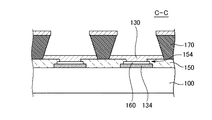
前記基板の上側に形成された端子と、
前記端子と電気的に接続する発光部と、
を備え、
前記端子は、
第1層と、
前記第1層よりも上側に位置し、前記第1層よりも柔らかい第2層と、
を備える発光装置である。
前記基板に、前記端子に接続する発光部を形成する工程と、
を備え、
前記端子を形成する工程は、
スパッタリングにより第1層を形成する工程と、
前記スパッタリングの入力電力を下げることにより、前記第1層より柔らかい第2層を前記第1層の上に形成する工程と、
を含む発光装置の製造方法である。
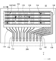
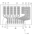
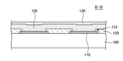
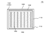
図4は、実施例1に係る発光装置10の平面図である。図5は、図4から隔壁170、第2電極130、有機層120、及び絶縁層150を取り除いた図である。図6は図4のA−A断面図であり、図7は図4のB−B断面図であり、図8は図4のC−C断面図である。
図9は、実施例2に係る発光装置10の構成を示す平面図である。図10は、図9から第2電極130を取り除いた図である。図11は、図10から有機層120を取り除いた図である。本図に示す発光装置10は照明装置である。このため、発光部140は基板100の縁を除いた領域に形成されている。
100 基板
110 第1電極
112 第1端子
112a 第1層
112b 第2層
114 引出配線
120 有機層
130 第2電極
132 第2端子
140 発光部
162 導体層
Claims (9)
- 基板と、
前記基板の上側に形成された端子と、
前記端子と電気的に接続する発光部と、
を備え、
前記端子は、
第1層と、
前記第1層よりも上側に位置し、前記第1層よりも柔らかい第2層と、
を備える発光装置。 - 請求項1に記載の発光装置において、
前記第2層は前記端子の表層に位置している発光装置。 - 請求項1又は2に記載の発光装置において、
前記第2層の密度は前記第1層の密度よりも低い発光装置。 - 請求項3に記載の発光装置において、前記第2層は前記第1層と同じ材料によって形成されている発光装置。
- 請求項1〜4のいずれか一項に記載の発光装置において、
前記基板は透光性を有しており、
前記端子は透明導電材料を用いて形成されている発光装置。 - 請求項5に記載の発光装置において、
前記透明導電材料はITO又はIZOである発光装置。 - 請求項1〜6のいずれか一項に記載の発光装置において、
前記基板は可撓性のある樹脂を有している発光装置。 - 請求項1〜6のいずれか一項に記載の発光装置において、
前記基板は厚み200μm以下のガラスを有している発光装置。 - 基板に端子を形成する工程と、
前記基板に、前記端子に接続する発光部を形成する工程と、
を備え、
前記端子を形成する工程は、
スパッタリングにより第1層を形成する工程と、
前記スパッタリングの入力電力を下げることにより、前記第1層より柔らかい第2層を前記第1層の上に形成する工程と、
を含む発光装置の製造方法。
Priority Applications (1)
| Application Number | Priority Date | Filing Date | Title |
|---|---|---|---|
| JP2014235863A JP2016100172A (ja) | 2014-11-20 | 2014-11-20 | 発光装置及び発光装置の製造方法 |
Applications Claiming Priority (1)
| Application Number | Priority Date | Filing Date | Title |
|---|---|---|---|
| JP2014235863A JP2016100172A (ja) | 2014-11-20 | 2014-11-20 | 発光装置及び発光装置の製造方法 |
Related Child Applications (1)
| Application Number | Title | Priority Date | Filing Date |
|---|---|---|---|
| JP2020000761A Division JP2020057627A (ja) | 2020-01-07 | 2020-01-07 | 発光装置 |
Publications (1)
| Publication Number | Publication Date |
|---|---|
| JP2016100172A true JP2016100172A (ja) | 2016-05-30 |
Family
ID=56077357
Family Applications (1)
| Application Number | Title | Priority Date | Filing Date |
|---|---|---|---|
| JP2014235863A Pending JP2016100172A (ja) | 2014-11-20 | 2014-11-20 | 発光装置及び発光装置の製造方法 |
Country Status (1)
| Country | Link |
|---|---|
| JP (1) | JP2016100172A (ja) |
Citations (4)
| Publication number | Priority date | Publication date | Assignee | Title |
|---|---|---|---|---|
| JPS63279597A (ja) * | 1987-05-08 | 1988-11-16 | Matsushita Electric Ind Co Ltd | 薄膜el素子およびその製造方法 |
| JPH03112088A (ja) * | 1989-09-27 | 1991-05-13 | Hitachi Chem Co Ltd | 薄膜el素子 |
| JP2001056480A (ja) * | 1999-08-19 | 2001-02-27 | Seiko Epson Corp | 電気光学装置及びその製造方法 |
| JP2007010834A (ja) * | 2005-06-29 | 2007-01-18 | Sumitomo Chemical Co Ltd | ディスプレイ用基板及びそれを用いたディスプレイ素子 |
-
2014
- 2014-11-20 JP JP2014235863A patent/JP2016100172A/ja active Pending
Patent Citations (4)
| Publication number | Priority date | Publication date | Assignee | Title |
|---|---|---|---|---|
| JPS63279597A (ja) * | 1987-05-08 | 1988-11-16 | Matsushita Electric Ind Co Ltd | 薄膜el素子およびその製造方法 |
| JPH03112088A (ja) * | 1989-09-27 | 1991-05-13 | Hitachi Chem Co Ltd | 薄膜el素子 |
| JP2001056480A (ja) * | 1999-08-19 | 2001-02-27 | Seiko Epson Corp | 電気光学装置及びその製造方法 |
| JP2007010834A (ja) * | 2005-06-29 | 2007-01-18 | Sumitomo Chemical Co Ltd | ディスプレイ用基板及びそれを用いたディスプレイ素子 |
Similar Documents
| Publication | Publication Date | Title |
|---|---|---|
| US20240099050A1 (en) | Light-emitting device | |
| JP2022164806A (ja) | 発光装置 | |
| JP2016119201A (ja) | 発光装置 | |
| JP6595066B2 (ja) | 発光装置の製造方法及び発光装置 | |
| JP2016095990A (ja) | 発光装置 | |
| JPWO2016151820A1 (ja) | 発光装置 | |
| JP7390508B2 (ja) | 発光装置及び発光装置の製造方法 | |
| JP2016100172A (ja) | 発光装置及び発光装置の製造方法 | |
| JP6555911B2 (ja) | 発光装置 | |
| JP6441306B2 (ja) | 発光装置 | |
| JP2016095991A (ja) | 発光装置 | |
| JP2016157645A (ja) | 発光装置 | |
| JPWO2017163331A1 (ja) | 発光装置、電子装置および発光装置の製造方法 | |
| JP2016186911A (ja) | 発光装置 | |
| JP6580336B2 (ja) | 発光装置 | |
| JP2023153346A (ja) | 発光装置 | |
| JP6499876B2 (ja) | 発光装置 | |
| JP6496138B2 (ja) | 発光装置 | |
| JP2019201004A (ja) | 発光装置 | |
| JP2016178061A (ja) | 発光装置の製造方法 | |
| JP2016143529A (ja) | 発光装置 | |
| JP2016184545A (ja) | 発光装置及び発光システム | |
| JP2016149315A (ja) | 発光装置の製造方法 | |
| WO2016129114A1 (ja) | 発光装置及び発光装置の製造方法 | |
| JP2016134328A (ja) | 発光装置 |
Legal Events
| Date | Code | Title | Description |
|---|---|---|---|
| A621 | Written request for application examination |
Free format text: JAPANESE INTERMEDIATE CODE: A621 Effective date: 20171005 |
|
| A977 | Report on retrieval |
Free format text: JAPANESE INTERMEDIATE CODE: A971007 Effective date: 20180820 |
|
| A131 | Notification of reasons for refusal |
Free format text: JAPANESE INTERMEDIATE CODE: A131 Effective date: 20180918 |
|
| A521 | Request for written amendment filed |
Free format text: JAPANESE INTERMEDIATE CODE: A523 Effective date: 20181114 |
|
| A131 | Notification of reasons for refusal |
Free format text: JAPANESE INTERMEDIATE CODE: A131 Effective date: 20190312 |
|
| A02 | Decision of refusal |
Free format text: JAPANESE INTERMEDIATE CODE: A02 Effective date: 20191008 |