JP2016111445A - Photographing apparatus - Google Patents
Photographing apparatus Download PDFInfo
- Publication number
- JP2016111445A JP2016111445A JP2014245238A JP2014245238A JP2016111445A JP 2016111445 A JP2016111445 A JP 2016111445A JP 2014245238 A JP2014245238 A JP 2014245238A JP 2014245238 A JP2014245238 A JP 2014245238A JP 2016111445 A JP2016111445 A JP 2016111445A
- Authority
- JP
- Japan
- Prior art keywords
- current
- column
- output line
- noise
- amount
- Prior art date
- Legal status (The legal status is an assumption and is not a legal conclusion. Google has not performed a legal analysis and makes no representation as to the accuracy of the status listed.)
- Pending
Links
Images
Landscapes
- Transforming Light Signals Into Electric Signals (AREA)
Abstract
【課題】 消費電流の増大を抑えつつ、効果的に電流源トランジスタに起因するノイズの発生を抑える。【解決手段】 列毎に電流を変更できる電流可変部を備え、電流可変部による電流設定は列毎のノイズ量に応じて変更する。【選択図】 図4PROBLEM TO BE SOLVED: To effectively suppress the generation of noise due to a current source transistor while suppressing an increase in current consumption. A current variable unit that can change a current for each column is provided, and a current setting by the current variable unit is changed according to a noise amount for each column. [Selection] Figure 4
Description
本発明は、撮像素子を用いた撮像装置に関するものである。 The present invention relates to an imaging apparatus using an imaging element.
近年、デジタルスチルカメラやデジタルビデオカメラなどの撮像装置には、CMOS型固体撮像素子が広く用いられている。CMOS撮像素子の画素部は、フォトダイオード、転送トランジスタ、フローティングディフュージョン、リセットトランジスタ、増幅トランジスタ、選択トランジスタから成る。また、垂直出力線と垂直出力線に接続された電流源トランジスタとを備え、画素部の増幅トランジスタと電流源トランジスタとが垂直出力線を介してソースフォロアを構成し、垂直出力線上の電位が外部に読み出される(特許文献1)。 In recent years, CMOS type solid-state imaging devices have been widely used in imaging devices such as digital still cameras and digital video cameras. The pixel portion of the CMOS image sensor includes a photodiode, a transfer transistor, a floating diffusion, a reset transistor, an amplification transistor, and a selection transistor. In addition, a vertical output line and a current source transistor connected to the vertical output line are provided, and the amplification transistor and the current source transistor of the pixel portion form a source follower via the vertical output line, and the potential on the vertical output line is external (Patent Document 1).
電流源トランジスタのゲート絶縁膜中にトラップ順位が存在すると、ノイズのパワースペクトルが周波数fの逆数に比例する1/fノイズが発生することがある。特許文献1のような構成の撮像装置では、電流源トランジスタで1/fノイズが発生すると、垂直出力線を流れる電流に揺らぎが発生する。その結果、画素部の増幅トランジスタの出力信号にノイズが発生する。このようなノイズの発生量は、製造上の影響により垂直出力線毎に差が生じやすく、ノイズ量の多い垂直出力線の部分があった場合には、線状のノイズとして目立つ可能性がある。また、1/fノイズのノイズ量は以下の式で表わされる。
v2=K/(LWI)
v:ノイズ量
L:トランジスタゲート長
W:トランジスタゲート幅
I:電流
If a trap order exists in the gate insulating film of the current source transistor, 1 / f noise in which the noise power spectrum is proportional to the reciprocal of the frequency f may occur. In the imaging apparatus configured as in Patent Document 1, when 1 / f noise occurs in the current source transistor, fluctuation occurs in the current flowing through the vertical output line. As a result, noise is generated in the output signal of the amplification transistor in the pixel portion. The amount of such noise is likely to be different for each vertical output line due to manufacturing effects, and if there is a portion of the vertical output line with a large amount of noise, it may be noticeable as linear noise. . Further, the noise amount of 1 / f noise is expressed by the following equation.
v 2 = K / (LWI)
v: Noise amount L: Transistor gate length W: Transistor gate width I: Current
したがって、垂直出力線の電流を増やすことにより、1/fノイズを低減させることが可能である。 Therefore, it is possible to reduce 1 / f noise by increasing the current of the vertical output line.
しかしながら、垂直出力線の電流を増やすとセンサ全体の消費電力が増加して電池の消耗が早くなり、或いは発熱による暗電流増加により撮影画質が劣化する。 However, when the current of the vertical output line is increased, the power consumption of the entire sensor is increased and the battery is consumed quickly, or the image quality is deteriorated due to an increase in dark current due to heat generation.
本発明の目的は、消費電力の増大を抑制しつつ、効果的に電流源トランジスタの1/fノイズに起因する線状ノイズの発生を抑え、良好な画質を得ることが可能な撮像装置を提供することである。 An object of the present invention is to provide an imaging device capable of effectively suppressing the occurrence of linear noise due to 1 / f noise of a current source transistor and suppressing the increase in power consumption and obtaining a good image quality. It is to be.
本発明の撮像装置は、行列状に配置された複数の画素と、列毎に設けられ前記複数の画素から画素信号が出力される列出力線と、前記列出力線に電流を供給する電流源とを備えた撮像素子と、前記列出力線のノイズ量を列毎に検出する検出手段と、前記検出手段により検出されるノイズ量に応じて前記電流源が供給する電流を列毎に変更するように制御する制御手段と、を備えたことを特徴とする。 An imaging apparatus according to the present invention includes a plurality of pixels arranged in a matrix, a column output line that is provided for each column and outputs a pixel signal from the plurality of pixels, and a current source that supplies a current to the column output line An image sensor including: a detection unit that detects a noise amount of the column output line for each column; and a current supplied from the current source is changed for each column according to the noise amount detected by the detection unit. And a control means for controlling as described above.
本発明によれば、消費電力の増加を抑制しながら、高画質を得ることが可能な撮像装置を提供することが出来る。 According to the present invention, it is possible to provide an imaging apparatus capable of obtaining high image quality while suppressing an increase in power consumption.
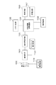
以下、本発明の一実施例について説明する。図1は、本発明の一実施例における撮像装置の全体ブロック図である。 Hereinafter, an embodiment of the present invention will be described. FIG. 1 is an overall block diagram of an imaging apparatus according to an embodiment of the present invention.
撮影レンズ1110は、被写体の光学像を撮像素子1101に結像させ、レンズ駆動回路1109によってズーム制御、フォーカス制御、絞り制御などが行われる。撮像素子1101は、撮影レンズ1110で結像された被写体を画像信号として取り込む。撮像素子1101の詳細は後述する。タイミング発生回路1102は、撮像素子1101に駆動タイミング信号を出力する。
The taking
信号処理回路1103は、撮像素子1101より出力される画像信号に対して、アナログデジタル変換処理や各種の補正処理を施す。全体制御・演算回路1104は、各種演算と撮像装置全体を制御する。全体制御・演算回路1104は、不図示のホワイトバランス調整部を備え、撮影画像の各色画素信号にホワイトバランスを乗算しホワイトバランスを調整している。
The
メモリ1105は、画像データを一時的に記憶する。表示回路1106は、各種情報や撮影画像を表示する。半導体メモリ等の着脱可能な記録回路1107は、画像データの記録または読み出しを行う。操作回路1108は、デジタルカメラの操作部材のユーザによる操作を電気的に受け付けるものである。
The
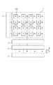
図2は、撮像素子1101の全体構成を示す図である。撮像素子1101は、画素領域1、垂直走査回路2、電流源回路3、読み出し回路4、水平走査回路5、出力アンプ6から構成される。
FIG. 2 is a diagram illustrating the overall configuration of the
画素領域1には、単位画素100が行列状に配置されている。ここでは、説明を簡単にするために4×4の16画素の配列を示してあるが、実用上はさらに多数の画素が配置される。各単位画素100には、複数種類の色のカラーフィルタが設けられている。
In the pixel region 1,
垂直走査回路2は、画素領域1の画素を1行単位で選択し、選択行の画素に対して駆動信号を送出する。
The
電流源回路3は、各列に設けられ、単位画素100と組になりソースフォロアを構成している。読み出し回路4は、各列に設けられ、単位画素100と電流源回路3とで構成されるソースフォロアの出力信号を増幅し、その出力信号をサンプルホールドする。
The current source circuit 3 is provided in each column and forms a source follower in combination with the
水平走査回路5は、列読み出し回路4でサンプルホールドされた信号を列毎に順次出力アンプ6に出力するための信号を送出する。出力アンプ6は、水平走査回路の動作により、列読み出し回路から出力された信号を外部に出力する。 The horizontal scanning circuit 5 sends out a signal for sequentially outputting the signal sampled and held by the column readout circuit 4 to the output amplifier 6 for each column. The output amplifier 6 outputs the signal output from the column readout circuit to the outside by the operation of the horizontal scanning circuit.
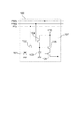
図3は、単位画素100の回路図である。図3に示すように、単位画素100は、フォトダイオード101、転送スイッチ102、フローティングディフュージョン103、リセットスイッチ104、増幅トランジスタ105、選択スイッチ106を含んでいる。
FIG. 3 is a circuit diagram of the
光電変換素子であるフォトダイオード101は、画素101へ入射した光を受光し、その受光量に応じた信号電荷を生成する光電変換部として機能する。転送スイッチ102は、転送パルス信号PTXによって駆動され、フォトダイオード101で生成された信号電荷をフローティングディフュージョン103に転送する。
The
フローティングディフュージョン103は、フォトダイオード101から転送された電荷を一時的に保持するとともに、保持した電荷を電圧信号に変換する電荷電圧変換部として機能する。増幅トランジスタ105は、ソースフォロアMOSトランジスタであり、フローティングディフュージョン103に保持した電荷に基づく電圧信号を増幅して、画素信号として出力する。
The
リセットスイッチ104は、リセットパルス信号PRESによって駆動され、フローティングディフュージョン103の電位を基準電位VDDにリセットする。選択スイッチ106は、垂直選択パルス信号PSELによって駆動され、増幅トランジスタ105で増幅された画素信号を垂直出力線(列出力線)107に出力する。
The
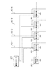
次に、図4を用いて、電流源回路3の詳細を説明する。まず、全ての列の基準となる定電流源となる基準電流回路201は、後述する電流可変回路R1〜R4の基準電流を供給する。基準電流回路201は、垂直出力線に設置されるMOSトランジスタや供給電流値を決定する抵抗などで構成されているものが一般的であるが、ここでの詳細説明は割愛する。
Next, details of the current source circuit 3 will be described with reference to FIG. First, a reference
また、2次元行列状の各列の画素に共通に接続されている複数の垂直出力線107−1〜107−n(本実施例では4列であるため、107−4)は、各列毎に供給する電流値を変更するための電流可変回路R1〜R4が接続される。 In addition, a plurality of vertical output lines 107-1 to 107-n (in this embodiment, there are four columns, 107-4) connected in common to the pixels in each column of a two-dimensional matrix are provided for each column. The variable current circuits R1 to R4 for changing the current value supplied to the are connected.
電流可変回路R1〜R4は、基準電流回路201から供給される基準電流に対して、垂直出力線107−1〜107−4の各列に供給する電流値を設定するものである。電流可変回路R1〜R4の電流設定値は、制御手段である制御ロジック回路202からの制御信号により列毎に制御されるものである。
The current variable circuits R1 to R4 set a current value supplied to each column of the vertical output lines 107-1 to 107-4 with respect to the reference current supplied from the reference
なお、列毎の定電流量は、例えば、電流可変回路R1〜R4の内部にある複数のサイズの異なるトランジスタを選択的に切り替えるにより、複数段階の変更を可能とするものでよいが、それに限ったものではない。 The constant current amount for each column may be changed in a plurality of stages by selectively switching, for example, a plurality of transistors having different sizes in the current variable circuits R1 to R4. Not a thing.
また、制御ロジック回路202についても、例えば、シリアル通信で各列に対して数ビットの設定を送るなどの周知の制御により、電流可変回路R1〜R4の内部設定を変更可能なものなどであればよい。
For the
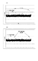
図5は、垂直出力線毎のノイズ量の面内ばらつきを表した一例のグラフである。ここでは、一般的なデジタルカメラなどで使用しているような数千列分のデータを示す。図5は、列毎にノイズ量を検出するために、撮像素子の暗時の出力信号のばらつきσを列毎に算出し、算出した列毎のσの平均値σaveとの比率σ/σaveを求めたものである。 FIG. 5 is an example graph showing in-plane variation in noise amount for each vertical output line. Here, data for thousands of columns used in a general digital camera or the like is shown. In FIG. 5, in order to detect the noise amount for each column, the variation σ of the output signal in the dark of the image sensor is calculated for each column, and the ratio σ / σave with the average value σave of the calculated σ for each column is calculated. It is what I have sought.
図5(a)は、垂直出力線の供給電流値として、全列の垂直出力線に対して第1の電流値の電流が供給されるように設定されている状態を示している。ノイズ検出手段によりノイズ量を列毎に検出した場合に、図5(a)のようにσ/σaveが大きい列が検出される。この状態において、検出されたノイズ量が第1の閾値(ノイズ判定閾値1)よりも大きい列の垂直出力線(列出力線)を記憶し、記憶した列の垂直出力線に第1の電流値よりも大きい第2の電流値を供給するように制御ロジック回路5が制御する。このような制御により、図5(b)のように、σ/σaveが大きい列のノイズ量を抑制することが出来る。 FIG. 5A shows a state in which the current of the first current value is set to be supplied to the vertical output lines of all columns as the supply current value of the vertical output lines. When the noise amount is detected for each column by the noise detection means, a column having a large σ / σave is detected as shown in FIG. In this state, the vertical output line (column output line) of the column in which the detected noise amount is larger than the first threshold (noise determination threshold 1) is stored, and the first current value is stored in the stored vertical output line. The control logic circuit 5 performs control so as to supply a second current value larger than that. By such control, as shown in FIG. 5B, it is possible to suppress the amount of noise in a column having a large σ / σave.
なお、ノイズ量の大きい列の検出については、例えば、製造時に複数毎の画像データから各画素の最大値Maxと最小値Minの差分を求めてもよいし、カメラの起動時に暗画像を取得し、本撮影前に検出及び記憶を行う方式でも構わない。 For detection of a column with a large amount of noise, for example, the difference between the maximum value Max and the minimum value Min of each pixel may be obtained from a plurality of image data at the time of manufacture, or a dark image is acquired when the camera is activated. A method of performing detection and storage before the actual photographing may be used.
上記実施例において、検出されたノイズ量の大きい列の垂直出力線の定電流量を第1の電流値よりも大きい第2の電流量にすることで、ノイズ量の大きな列のノイズ量を抑制することが出来るが、それにより消費電力が増大してしまう。そこで、定電流量を下げてもよい列を検出して、消費電流の増大を抑制してもよい。 In the embodiment described above, the amount of noise in a column with a large amount of noise is suppressed by setting the constant current amount of the detected vertical output line in the column with a large amount of noise to a second amount of current that is larger than the first current value. This can increase power consumption. Therefore, a column in which the constant current amount may be decreased may be detected to suppress an increase in current consumption.
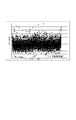
図6は、図5と同様に、垂直出力線毎のノイズ量の面内ばらつきを表したグラフである。列毎にノイズ量を検出するために、撮像素子の暗時の出力信号のばらつきσを列毎に算出し、算出した列毎のσの平均値σaveとの比率σ/σaveを求めたものである。図6は、垂直出力線の供給電流値として、全列の垂直出力線に対して第1の電流値よりも小さい第3の電流値の電流が供給されるように設定されている状態を示している。すなわち、小さい電流値を供給するように駆動することにより、σ/σaveが大きくなる状況を設定したものである。 FIG. 6 is a graph showing the in-plane variation of the noise amount for each vertical output line, as in FIG. In order to detect the noise amount for each column, the variation σ of the output signal in the dark of the image sensor is calculated for each column, and the ratio σ / σave with the average value σave of the calculated σ for each column is obtained. is there. FIG. 6 shows a state in which a current having a third current value smaller than the first current value is supplied to the vertical output lines of all columns as the supply current value of the vertical output lines. ing. That is, a situation is set in which σ / σave increases by driving to supply a small current value.
この状況で、前記第1の閾値よりも小さい第2の閾値(ノイズ判定閾値2)を下回る列の垂直出力線(列出力線)を記憶する。そして、記憶した列の垂直出力線に第1の電流値よりも小さい第3の電流値を供給するように制御ロジック回路5が制御する。 In this situation, the vertical output line (column output line) of the column that falls below the second threshold value (noise determination threshold value 2) that is smaller than the first threshold value is stored. Then, the control logic circuit 5 controls to supply a third current value smaller than the first current value to the vertical output line of the stored column.
このように制御することで、通常のノイズ量の列の垂直出力線には第1の電流値が供給される。また、検出されたノイズ量がノイズ判定閾値1を超えている列の垂直出力線には第2の電流値が供給される。さらに、検出されたノイズ量がノイズ判定閾値2を下回る列の垂直出力線には第3の電流値が供給されるように制御することで、トータル的な消費電流の増大を抑制しつつ、ノイズ量の大きな列のノイズ低減を図ることが出来る。
By controlling in this way, the first current value is supplied to the vertical output line of the normal noise amount column. Further, the second current value is supplied to the vertical output line of the column in which the detected noise amount exceeds the noise determination threshold value 1. Further, the control is performed so that the third current value is supplied to the vertical output line of the column in which the detected noise amount is lower than the
1 画素領域
2 垂直走査回路
3 電流源回路
4 読み出し回路
5 水平走査回路
6 出力アンプ
100 単位画素
101 フォトダイオード
102 転送スイッチ
103 フローティングディフュージョン
104 リセットスイッチ
105 増幅トランジスタ
106 選択スイッチ
107−1〜107−4 垂直出力線
201 基準電流回路
202 制御ロジック回路
R1〜R4 電流可変回路
1
Claims (4)
前記列出力線のノイズ量を列毎に検出する検出手段と、
前記検出手段により検出されるノイズ量に応じて前記電流源が供給する電流を列毎に変更するように制御する制御手段と、
を備えたことを特徴とする撮像装置。 An imaging device comprising: a plurality of pixels arranged in a matrix; a column output line that is provided for each column and outputs a pixel signal from the plurality of pixels; and a current source that supplies a current to the column output line; ,
Detecting means for detecting the noise amount of the column output line for each column;
Control means for controlling the current supplied by the current source to change for each column according to the amount of noise detected by the detection means;
An imaging apparatus comprising:
Priority Applications (1)
| Application Number | Priority Date | Filing Date | Title |
|---|---|---|---|
| JP2014245238A JP2016111445A (en) | 2014-12-03 | 2014-12-03 | Photographing apparatus |
Applications Claiming Priority (1)
| Application Number | Priority Date | Filing Date | Title |
|---|---|---|---|
| JP2014245238A JP2016111445A (en) | 2014-12-03 | 2014-12-03 | Photographing apparatus |
Publications (1)
| Publication Number | Publication Date |
|---|---|
| JP2016111445A true JP2016111445A (en) | 2016-06-20 |
Family
ID=56124970
Family Applications (1)
| Application Number | Title | Priority Date | Filing Date |
|---|---|---|---|
| JP2014245238A Pending JP2016111445A (en) | 2014-12-03 | 2014-12-03 | Photographing apparatus |
Country Status (1)
| Country | Link |
|---|---|
| JP (1) | JP2016111445A (en) |
-
2014
- 2014-12-03 JP JP2014245238A patent/JP2016111445A/en active Pending
Similar Documents
| Publication | Publication Date | Title |
|---|---|---|
| US11743595B2 (en) | Method and apparatus providing pixel array having automatic light control pixels and image capture pixels | |
| US11089256B2 (en) | Image sensor with correction of detection error | |
| JP6635027B2 (en) | Image sensor, gain control method, program, and electronic device | |
| US10205898B2 (en) | Minimizing a data pedestal level in an image sensor | |
| US10785423B2 (en) | Image sensor, image capturing apparatus, and image capturing method | |
| TWI511557B (en) | Solid-state imaging device and driving method thereof, and electronic device using the same | |
| US10313588B2 (en) | Image capturing system and control method of image capturing system | |
| US9635241B2 (en) | Image capturing apparatus and method of controlling image capturing apparatus | |
| JP5335465B2 (en) | Solid-state imaging device and imaging apparatus | |
| JP6635310B2 (en) | Image sensor, control method, program, and electronic device | |
| JP2016019232A (en) | Imaging device and imaging apparatus | |
| JP2016111445A (en) | Photographing apparatus | |
| JP6362099B2 (en) | Imaging apparatus, control method therefor, program, and storage medium | |
| JP2018093301A (en) | Image pick-up device and control method of the same | |
| JP2017085377A (en) | Imaging apparatus and its control method, program, and storage medium | |
| JP6700754B2 (en) | Imaging device, control method thereof, program, and storage medium | |
| JP5737924B2 (en) | Imaging device | |
| JP5376966B2 (en) | Imaging device and imaging apparatus | |
| JP6393087B2 (en) | Imaging device and imaging apparatus | |
| JP2016208421A (en) | Imaging apparatus and control method of the same | |
| JP2016039406A (en) | Solid-state imaging device and imaging apparatus |