JP2016122965A - 負荷駆動回路 - Google Patents
負荷駆動回路 Download PDFInfo
- Publication number
- JP2016122965A JP2016122965A JP2014261586A JP2014261586A JP2016122965A JP 2016122965 A JP2016122965 A JP 2016122965A JP 2014261586 A JP2014261586 A JP 2014261586A JP 2014261586 A JP2014261586 A JP 2014261586A JP 2016122965 A JP2016122965 A JP 2016122965A
- Authority
- JP
- Japan
- Prior art keywords
- voltage
- terminal
- circuit
- load
- clamp
- Prior art date
- Legal status (The legal status is an assumption and is not a legal conclusion. Google has not performed a legal analysis and makes no representation as to the accuracy of the status listed.)
- Granted
Links
- 239000003990 capacitor Substances 0.000 claims abstract description 27
- 230000001629 suppression Effects 0.000 claims abstract description 7
- 230000000630 rising effect Effects 0.000 abstract 1
- 238000001514 detection method Methods 0.000 description 8
- 238000010586 diagram Methods 0.000 description 4
- 230000007423 decrease Effects 0.000 description 1
Images


Classifications
-
- H—ELECTRICITY
- H03—ELECTRONIC CIRCUITRY
- H03K—PULSE TECHNIQUE
- H03K17/00—Electronic switching or gating, i.e. not by contact-making and –breaking
- H03K17/51—Electronic switching or gating, i.e. not by contact-making and –breaking characterised by the components used
- H03K17/56—Electronic switching or gating, i.e. not by contact-making and –breaking characterised by the components used by the use, as active elements, of semiconductor devices
- H03K17/687—Electronic switching or gating, i.e. not by contact-making and –breaking characterised by the components used by the use, as active elements, of semiconductor devices the devices being field-effect transistors
-
- H—ELECTRICITY
- H03—ELECTRONIC CIRCUITRY
- H03K—PULSE TECHNIQUE
- H03K17/00—Electronic switching or gating, i.e. not by contact-making and –breaking
- H03K17/08—Modifications for protecting switching circuit against overcurrent or overvoltage
- H03K17/081—Modifications for protecting switching circuit against overcurrent or overvoltage without feedback from the output circuit to the control circuit
- H03K17/0814—Modifications for protecting switching circuit against overcurrent or overvoltage without feedback from the output circuit to the control circuit by measures taken in the output circuit
- H03K17/08148—Modifications for protecting switching circuit against overcurrent or overvoltage without feedback from the output circuit to the control circuit by measures taken in the output circuit in composite switches
-
- H—ELECTRICITY
- H01—ELECTRIC ELEMENTS
- H01F—MAGNETS; INDUCTANCES; TRANSFORMERS; SELECTION OF MATERIALS FOR THEIR MAGNETIC PROPERTIES
- H01F7/00—Magnets
- H01F7/06—Electromagnets; Actuators including electromagnets
- H01F7/064—Circuit arrangements for actuating electromagnets
-
- H—ELECTRICITY
- H02—GENERATION; CONVERSION OR DISTRIBUTION OF ELECTRIC POWER
- H02H—EMERGENCY PROTECTIVE CIRCUIT ARRANGEMENTS
- H02H11/00—Emergency protective circuit arrangements for preventing the switching-on in case an undesired electric working condition might result
- H02H11/002—Emergency protective circuit arrangements for preventing the switching-on in case an undesired electric working condition might result in case of inverted polarity or connection; with switching for obtaining correct connection
-
- H—ELECTRICITY
- H03—ELECTRONIC CIRCUITRY
- H03K—PULSE TECHNIQUE
- H03K17/00—Electronic switching or gating, i.e. not by contact-making and –breaking
- H03K17/51—Electronic switching or gating, i.e. not by contact-making and –breaking characterised by the components used
- H03K17/56—Electronic switching or gating, i.e. not by contact-making and –breaking characterised by the components used by the use, as active elements, of semiconductor devices
- H03K17/60—Electronic switching or gating, i.e. not by contact-making and –breaking characterised by the components used by the use, as active elements, of semiconductor devices the devices being bipolar transistors
- H03K17/64—Electronic switching or gating, i.e. not by contact-making and –breaking characterised by the components used by the use, as active elements, of semiconductor devices the devices being bipolar transistors having inductive loads
-
- H—ELECTRICITY
- H02—GENERATION; CONVERSION OR DISTRIBUTION OF ELECTRIC POWER
- H02M—APPARATUS FOR CONVERSION BETWEEN AC AND AC, BETWEEN AC AND DC, OR BETWEEN DC AND DC, AND FOR USE WITH MAINS OR SIMILAR POWER SUPPLY SYSTEMS; CONVERSION OF DC OR AC INPUT POWER INTO SURGE OUTPUT POWER; CONTROL OR REGULATION THEREOF
- H02M1/00—Details of apparatus for conversion
- H02M1/0003—Details of control, feedback or regulation circuits
- H02M1/0025—Arrangements for modifying reference values, feedback values or error values in the control loop of a converter
-
- H—ELECTRICITY
- H03—ELECTRONIC CIRCUITRY
- H03K—PULSE TECHNIQUE
- H03K2217/00—Indexing scheme related to electronic switching or gating, i.e. not by contact-making or -breaking covered by H03K17/00
- H03K2217/0081—Power supply means, e.g. to the switch driver
Landscapes
- Physics & Mathematics (AREA)
- Electromagnetism (AREA)
- Engineering & Computer Science (AREA)
- Power Engineering (AREA)
- Power Conversion In General (AREA)
- Electronic Switches (AREA)
Abstract
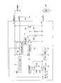
【解決手段】スイッチング素子Q1、電源端子Vccに入力される電圧Eよりも低い第1の基準電圧V1と出力端子OUTの電圧とを比較してスイッチング素子Q1がオフ状態で且つ出力端子に負荷20が接続されていない負荷オープン状態を検出する第1のコンパレータCP1、電圧Eよりも低く且つクランプ電圧よりも高い第2の基準電圧V2と出力端子OUTの電圧とを比較して出力天絡状態を検出する第2のコンパレータCP2、負荷オープン状態である場合に、出力端子の電圧を第1の基準電圧よりも高く且つ電圧Eよりも低いクランプ電圧にクランプするクランプ回路14、コンデンサC1、電源の電圧Eに基づき生成された定電圧により充電電流をamp端子に供給するブートストラップ回路10、第1のコンパレータが負荷オープン状態を検出した場合にクランプ回路のクランプ電圧の上昇を抑止するクランプ電圧上昇抑止回路16とを備える。
【選択図】図1
Description
12 バッファ回路
13 制御回路
14 クランプ回路
15 定電流源
16 充電電流停止回路
17 放電停止回路
20 負荷
BS ブートストラップ回路
Q1 スイッチング素子
E 電源
C1 コンデンサ
Vcc 電源端子
OUT 出力端子
CP1 第1のコンパレータ
CP2 第2のコンパレータ
Claims (4)
- 電源に接続される第1の端子と、負荷に接続される第2の端子と、前記第1の端子と前記第2の端子との間に接続されたスイッチング素子と、
前記第1の端子に入力される入力電圧よりも低い第1の基準電圧と前記第2の端子の電圧とを比較することにより前記スイッチング素子がオフ状態で且つ前記第2の端子に前記負荷が接続されていない負荷オープン状態を検出する第1のコンパレータと、
前記負荷オープン状態である場合に、前記第2の端子の電圧を前記第1の基準電圧よりも高く且つ前記入力電圧よりも低いクランプ電圧にクランプするクランプ回路と、
前記入力電圧よりも低く且つ前記クランプ電圧よりも高い第2の基準電圧と前記第2の端子の電圧とを比較することにより前記スイッチング素子がオフ状態で且つ前記第2の端子が前記電源に接続される出力天絡状態を検出する第2のコンパレータと、
一端が前記第2の端子に接続され他端が第3の端子に接続されるコンデンサと、
前記第1の端子の電源の電圧に基づき定電圧を生成し、定電圧により充電電流を前記第3の端子に供給するブートストラップ回路と、
前記第1のコンパレータが負荷オープン状態を検出した場合に、前記クランプ回路のクランプ電圧の上昇を抑止するクランプ電圧上昇抑止回路と、
を備えることを特微とする負荷駆動回路。 - 前記クランプ電圧上昇抑止回路は、前記第1のコンパレータが負荷オープン状態を検出した場合に、前記ブートストラップ回路から前記第3の端子と前記コンデンサを介して前記クランプ回路に流れる電流を停止させる充電電流停止回路からなることを特徴とする請求項1記載の負荷駆動回路。
- 前記クランプ電圧上昇抑止回路は、前記第1のコンパレータが負荷オープン状態を検出した場合に、前記コンデンサの放電を停止させる放電停止回路からなることを特徴とする請求項1記載の負荷駆動回路。
- 電源に接続される第1の端子と、負荷に接続される第2の端子と、前記第1の端子と前記第2の端子との間に接続されたスイッチング素子と、
前記第1の端子に入力される入力電圧よりも低い第1の基準電圧と前記第2の端子の電圧とを比較することにより前記スイッチング素子がオフ状態で且つ前記第2の端子に前記負荷が接続されていない負荷オープン状態を検出する第1のコンパレータと、
前記負荷オープン状態である場合に、前記第2の端子の電圧を前記第1の基準電圧よりも高く且つ前記入力電圧よりも低いクランプ電圧にクランプするクランプ回路と、
前記入力電圧よりも低く且つ前記クランプ電圧よりも高い第2の基準電圧と前記第2の端子の電圧とを比較することにより出力天絡状態を検出する第2のコンパレータと、
一端が前記第2の端子に接続され他端が第3の端子に接続されるコンデンサと、
前記第1の端子の電源の電圧に基づき定電圧を生成し、定電圧により充電電流を前記第3の端子に供給するブートストラップ回路とを備え、
前記第2のコンパレータは、前記第1のコンパレータが負荷オープン状態を検出した場合に、前記第2の基準電圧を、前記ブートストラップ回路から前記第3の端子と前記コンデンサを介して前記クランプ回路に流れる電流を含む電流により発生する電圧よりも高い電圧で且つ前記入力電圧よりも低い電圧に設定することを特微とする負荷駆動回路。
Priority Applications (4)
| Application Number | Priority Date | Filing Date | Title |
|---|---|---|---|
| JP2014261586A JP6405998B2 (ja) | 2014-12-25 | 2014-12-25 | 負荷駆動回路 |
| EP15199762.4A EP3038223B1 (en) | 2014-12-25 | 2015-12-14 | Load driving circuit |
| CN201510940215.6A CN105743475B (zh) | 2014-12-25 | 2015-12-16 | 负载驱动电路 |
| US14/972,803 US9444447B2 (en) | 2014-12-25 | 2015-12-17 | Load drive circuit |
Applications Claiming Priority (1)
| Application Number | Priority Date | Filing Date | Title |
|---|---|---|---|
| JP2014261586A JP6405998B2 (ja) | 2014-12-25 | 2014-12-25 | 負荷駆動回路 |
Publications (2)
| Publication Number | Publication Date |
|---|---|
| JP2016122965A true JP2016122965A (ja) | 2016-07-07 |
| JP6405998B2 JP6405998B2 (ja) | 2018-10-17 |
Family
ID=54849815
Family Applications (1)
| Application Number | Title | Priority Date | Filing Date |
|---|---|---|---|
| JP2014261586A Expired - Fee Related JP6405998B2 (ja) | 2014-12-25 | 2014-12-25 | 負荷駆動回路 |
Country Status (4)
| Country | Link |
|---|---|
| US (1) | US9444447B2 (ja) |
| EP (1) | EP3038223B1 (ja) |
| JP (1) | JP6405998B2 (ja) |
| CN (1) | CN105743475B (ja) |
Cited By (1)
| Publication number | Priority date | Publication date | Assignee | Title |
|---|---|---|---|---|
| DE112020002140T5 (de) | 2019-05-31 | 2022-01-13 | Hitachi Astemo, Ltd. | Elektronische schaltung und sensorsystem |
Families Citing this family (5)
| Publication number | Priority date | Publication date | Assignee | Title |
|---|---|---|---|---|
| TWI687047B (zh) * | 2017-04-10 | 2020-03-01 | 力智電子股份有限公司 | 驅動電路及其控制方法 |
| US10742121B2 (en) * | 2018-06-29 | 2020-08-11 | Dialog Semiconductor Inc. | Boot strap capacitor charging for switching power converters |
| JP7085017B2 (ja) * | 2018-11-06 | 2022-06-15 | 日立Astemo株式会社 | 負荷駆動装置及び変速機の駆動システム |
| CN112994679A (zh) * | 2021-04-20 | 2021-06-18 | 深圳市拓尔微电子有限责任公司 | 驱动电路及控制芯片 |
| CN117155126B (zh) * | 2023-03-14 | 2024-06-25 | 荣耀终端有限公司 | 终端设备及控制方法 |
Citations (8)
| Publication number | Priority date | Publication date | Assignee | Title |
|---|---|---|---|---|
| JP2005217497A (ja) * | 2004-01-27 | 2005-08-11 | Denso Corp | 半導体集積回路装置用負荷駆動回路 |
| JP2008092277A (ja) * | 2006-10-02 | 2008-04-17 | Hitachi Ltd | 負荷駆動回路 |
| JP2011259223A (ja) * | 2010-06-09 | 2011-12-22 | Denso Corp | スイッチング装置 |
| JP2012139096A (ja) * | 2004-01-28 | 2012-07-19 | Renesas Electronics Corp | 半導体装置 |
| JP2012175503A (ja) * | 2011-02-23 | 2012-09-10 | Denso Corp | 負荷駆動装置 |
| JP2013016959A (ja) * | 2011-07-01 | 2013-01-24 | Sanken Electric Co Ltd | 負荷駆動回路 |
| WO2013047005A1 (ja) * | 2011-09-29 | 2013-04-04 | 富士電機株式会社 | 負荷駆動回路 |
| JP2014023272A (ja) * | 2012-07-18 | 2014-02-03 | Denso Corp | スイッチング電源回路 |
Family Cites Families (13)
| Publication number | Priority date | Publication date | Assignee | Title |
|---|---|---|---|---|
| US4065678A (en) * | 1976-07-02 | 1977-12-27 | Motorola, Inc. | Clamped push-pull driver circuit with output feedback |
| KR100439045B1 (ko) * | 2001-06-29 | 2004-07-05 | 주식회사 하이닉스반도체 | 워드 라인 전압 클램핑 회로 |
| TW200525867A (en) * | 2004-01-21 | 2005-08-01 | Renesas Tech Corp | Voltage clamp circuit, switching power supply apparatus, semiconductor IC device, and voltage level converting circuit |
| US7368957B2 (en) * | 2006-07-21 | 2008-05-06 | Picor Corporation | Capacitively coupled floating gate driver |
| US7898781B2 (en) * | 2008-08-01 | 2011-03-01 | Sensata Technologies Massachusetts, Inc. | Arc fault detection apparatus employing a comparator with a continuously variable threshold |
| JP2011146901A (ja) * | 2010-01-14 | 2011-07-28 | Denso Corp | 駆動装置 |
| JP5556404B2 (ja) * | 2010-06-11 | 2014-07-23 | サンケン電気株式会社 | スイッチング電源装置 |
| JP5656072B2 (ja) * | 2011-01-25 | 2015-01-21 | サンケン電気株式会社 | Dc−dcコンバータ |
| CN102832810B (zh) * | 2012-08-30 | 2015-04-08 | 成都芯源系统有限公司 | 自举电压刷新控制电路、电压转换电路及相关控制方法 |
| JP6070164B2 (ja) * | 2012-12-21 | 2017-02-01 | サンケン電気株式会社 | スイッチング電源装置 |
| CN103023286B (zh) * | 2012-12-28 | 2015-04-01 | 矽力杰半导体技术(杭州)有限公司 | 一种自举电容掉电恢复电路及开关电源电路 |
| US9484758B2 (en) * | 2013-02-05 | 2016-11-01 | Apple Inc. | Hybrid bootstrap capacitor refresh technique for charger/converter |
| CN104079276B (zh) * | 2014-06-28 | 2017-01-11 | 柳州长虹机器制造公司 | 一种宽电压适应性的高效率智能高边电子负载开关 |
-
2014
- 2014-12-25 JP JP2014261586A patent/JP6405998B2/ja not_active Expired - Fee Related
-
2015
- 2015-12-14 EP EP15199762.4A patent/EP3038223B1/en active Active
- 2015-12-16 CN CN201510940215.6A patent/CN105743475B/zh active Active
- 2015-12-17 US US14/972,803 patent/US9444447B2/en active Active
Patent Citations (8)
| Publication number | Priority date | Publication date | Assignee | Title |
|---|---|---|---|---|
| JP2005217497A (ja) * | 2004-01-27 | 2005-08-11 | Denso Corp | 半導体集積回路装置用負荷駆動回路 |
| JP2012139096A (ja) * | 2004-01-28 | 2012-07-19 | Renesas Electronics Corp | 半導体装置 |
| JP2008092277A (ja) * | 2006-10-02 | 2008-04-17 | Hitachi Ltd | 負荷駆動回路 |
| JP2011259223A (ja) * | 2010-06-09 | 2011-12-22 | Denso Corp | スイッチング装置 |
| JP2012175503A (ja) * | 2011-02-23 | 2012-09-10 | Denso Corp | 負荷駆動装置 |
| JP2013016959A (ja) * | 2011-07-01 | 2013-01-24 | Sanken Electric Co Ltd | 負荷駆動回路 |
| WO2013047005A1 (ja) * | 2011-09-29 | 2013-04-04 | 富士電機株式会社 | 負荷駆動回路 |
| JP2014023272A (ja) * | 2012-07-18 | 2014-02-03 | Denso Corp | スイッチング電源回路 |
Cited By (2)
| Publication number | Priority date | Publication date | Assignee | Title |
|---|---|---|---|---|
| DE112020002140T5 (de) | 2019-05-31 | 2022-01-13 | Hitachi Astemo, Ltd. | Elektronische schaltung und sensorsystem |
| US12047062B2 (en) | 2019-05-31 | 2024-07-23 | Hitachi Astemo, Ltd. | Electronic circuit and sensor system |
Also Published As
| Publication number | Publication date |
|---|---|
| EP3038223B1 (en) | 2018-04-04 |
| CN105743475A (zh) | 2016-07-06 |
| JP6405998B2 (ja) | 2018-10-17 |
| CN105743475B (zh) | 2020-10-09 |
| US20160191045A1 (en) | 2016-06-30 |
| EP3038223A1 (en) | 2016-06-29 |
| US9444447B2 (en) | 2016-09-13 |
Similar Documents
| Publication | Publication Date | Title |
|---|---|---|
| JP6405998B2 (ja) | 負荷駆動回路 | |
| JP5315026B2 (ja) | 半導体装置 | |
| TWI610528B (zh) | 升壓型切換調節器及電子機器 | |
| US8576529B2 (en) | Power stage control circuit | |
| JP6468150B2 (ja) | 負荷駆動装置 | |
| US10637237B2 (en) | Power switch circuit and power circuit with the same | |
| US8045310B2 (en) | Semiconductor device with overcurrent protection | |
| JP2013016959A (ja) | 負荷駆動回路 | |
| US20200195127A1 (en) | Protection circuit with a cut-off switch for power systems | |
| US8427804B2 (en) | Power amplifier | |
| CN106134050A (zh) | 驱动装置 | |
| US9640978B2 (en) | Protection circuit for an inverter as well as inverter system | |
| JP6229604B2 (ja) | 半導体スイッチング素子の制御回路 | |
| JPWO2023219031A5 (ja) | ||
| CN105717972A (zh) | 半导体器件以及电流限制方法 | |
| JP5953099B2 (ja) | 負荷制御および保護システム、並びにその動作および使用方法 | |
| JP6601026B2 (ja) | 半導体スイッチ回路及び半導体リレー回路 | |
| JP6519498B2 (ja) | スイッチング電源装置 | |
| JP7052517B2 (ja) | 負荷駆動装置 | |
| JP7119654B2 (ja) | 負荷駆動装置 | |
| KR101238663B1 (ko) | 아몰레드 구동용 파워 아이씨의 셧 다운 시 스위칭 전압 제한을 구현하는 동기식 승압형 컨버터 회로 | |
| JP4900321B2 (ja) | 過電流保護回路 | |
| JP5733237B2 (ja) | 制御回路 | |
| JP2017028596A (ja) | 半導体スイッチ回路及び半導体リレー回路 | |
| JP6844318B2 (ja) | 車載制御装置 |
Legal Events
| Date | Code | Title | Description |
|---|---|---|---|
| A621 | Written request for application examination |
Free format text: JAPANESE INTERMEDIATE CODE: A621 Effective date: 20170908 |
|
| A977 | Report on retrieval |
Free format text: JAPANESE INTERMEDIATE CODE: A971007 Effective date: 20180522 |
|
| A131 | Notification of reasons for refusal |
Free format text: JAPANESE INTERMEDIATE CODE: A131 Effective date: 20180703 |
|
| A521 | Request for written amendment filed |
Free format text: JAPANESE INTERMEDIATE CODE: A523 Effective date: 20180810 |
|
| TRDD | Decision of grant or rejection written | ||
| A01 | Written decision to grant a patent or to grant a registration (utility model) |
Free format text: JAPANESE INTERMEDIATE CODE: A01 Effective date: 20180821 |
|
| A61 | First payment of annual fees (during grant procedure) |
Free format text: JAPANESE INTERMEDIATE CODE: A61 Effective date: 20180903 |
|
| R150 | Certificate of patent or registration of utility model |
Ref document number: 6405998 Country of ref document: JP Free format text: JAPANESE INTERMEDIATE CODE: R150 |
|
| LAPS | Cancellation because of no payment of annual fees |