JP2016152255A - Semiconductor device - Google Patents
Semiconductor device Download PDFInfo
- Publication number
- JP2016152255A JP2016152255A JP2015027467A JP2015027467A JP2016152255A JP 2016152255 A JP2016152255 A JP 2016152255A JP 2015027467 A JP2015027467 A JP 2015027467A JP 2015027467 A JP2015027467 A JP 2015027467A JP 2016152255 A JP2016152255 A JP 2016152255A
- Authority
- JP
- Japan
- Prior art keywords
- region
- semiconductor region
- electrode
- type
- type semiconductor
- Prior art date
- Legal status (The legal status is an assumption and is not a legal conclusion. Google has not performed a legal analysis and makes no representation as to the accuracy of the status listed.)
- Ceased
Links
Images


















Classifications
-
- H—ELECTRICITY
- H10—SEMICONDUCTOR DEVICES; ELECTRIC SOLID-STATE DEVICES NOT OTHERWISE PROVIDED FOR
- H10D—INORGANIC ELECTRIC SEMICONDUCTOR DEVICES
- H10D84/00—Integrated devices formed in or on semiconductor substrates that comprise only semiconducting layers, e.g. on Si wafers or on GaAs-on-Si wafers
- H10D84/40—Integrated devices formed in or on semiconductor substrates that comprise only semiconducting layers, e.g. on Si wafers or on GaAs-on-Si wafers characterised by the integration of at least one component covered by groups H10D12/00 or H10D30/00 with at least one component covered by groups H10D10/00 or H10D18/00, e.g. integration of IGFETs with BJTs
- H10D84/401—Combinations of FETs or IGBTs with BJTs
-
- H—ELECTRICITY
- H10—SEMICONDUCTOR DEVICES; ELECTRIC SOLID-STATE DEVICES NOT OTHERWISE PROVIDED FOR
- H10D—INORGANIC ELECTRIC SEMICONDUCTOR DEVICES
- H10D48/00—Individual devices not covered by groups H10D1/00 - H10D44/00
- H10D48/30—Devices controlled by electric currents or voltages
- H10D48/32—Devices controlled by only the electric current supplied, or only the electric potential applied, to an electrode which does not carry the current to be rectified, amplified or switched
- H10D48/34—Bipolar devices
- H10D48/345—Bipolar transistors having ohmic electrodes on emitter-like, base-like, and collector-like regions
-
- H—ELECTRICITY
- H10—SEMICONDUCTOR DEVICES; ELECTRIC SOLID-STATE DEVICES NOT OTHERWISE PROVIDED FOR
- H10D—INORGANIC ELECTRIC SEMICONDUCTOR DEVICES
- H10D10/00—Bipolar junction transistors [BJT]
- H10D10/01—Manufacture or treatment
- H10D10/051—Manufacture or treatment of vertical BJTs
-
- H—ELECTRICITY
- H10—SEMICONDUCTOR DEVICES; ELECTRIC SOLID-STATE DEVICES NOT OTHERWISE PROVIDED FOR
- H10D—INORGANIC ELECTRIC SEMICONDUCTOR DEVICES
- H10D10/00—Bipolar junction transistors [BJT]
- H10D10/40—Vertical BJTs
-
- H—ELECTRICITY
- H10—SEMICONDUCTOR DEVICES; ELECTRIC SOLID-STATE DEVICES NOT OTHERWISE PROVIDED FOR
- H10D—INORGANIC ELECTRIC SEMICONDUCTOR DEVICES
- H10D10/00—Bipolar junction transistors [BJT]
- H10D10/60—Lateral BJTs
-
- H—ELECTRICITY
- H10—SEMICONDUCTOR DEVICES; ELECTRIC SOLID-STATE DEVICES NOT OTHERWISE PROVIDED FOR
- H10D—INORGANIC ELECTRIC SEMICONDUCTOR DEVICES
- H10D62/00—Semiconductor bodies, or regions thereof, of devices having potential barriers
- H10D62/10—Shapes, relative sizes or dispositions of the regions of the semiconductor bodies; Shapes of the semiconductor bodies
-
- H—ELECTRICITY
- H10—SEMICONDUCTOR DEVICES; ELECTRIC SOLID-STATE DEVICES NOT OTHERWISE PROVIDED FOR
- H10D—INORGANIC ELECTRIC SEMICONDUCTOR DEVICES
- H10D62/00—Semiconductor bodies, or regions thereof, of devices having potential barriers
- H10D62/10—Shapes, relative sizes or dispositions of the regions of the semiconductor bodies; Shapes of the semiconductor bodies
- H10D62/113—Isolations within a component, i.e. internal isolations
- H10D62/115—Dielectric isolations, e.g. air gaps
-
- H—ELECTRICITY
- H10—SEMICONDUCTOR DEVICES; ELECTRIC SOLID-STATE DEVICES NOT OTHERWISE PROVIDED FOR
- H10D—INORGANIC ELECTRIC SEMICONDUCTOR DEVICES
- H10D62/00—Semiconductor bodies, or regions thereof, of devices having potential barriers
- H10D62/10—Shapes, relative sizes or dispositions of the regions of the semiconductor bodies; Shapes of the semiconductor bodies
- H10D62/124—Shapes, relative sizes or dispositions of the regions of semiconductor bodies or of junctions between the regions
- H10D62/126—Top-view geometrical layouts of the regions or the junctions
-
- H—ELECTRICITY
- H10—SEMICONDUCTOR DEVICES; ELECTRIC SOLID-STATE DEVICES NOT OTHERWISE PROVIDED FOR
- H10D—INORGANIC ELECTRIC SEMICONDUCTOR DEVICES
- H10D62/00—Semiconductor bodies, or regions thereof, of devices having potential barriers
- H10D62/10—Shapes, relative sizes or dispositions of the regions of the semiconductor bodies; Shapes of the semiconductor bodies
- H10D62/13—Semiconductor regions connected to electrodes carrying current to be rectified, amplified or switched, e.g. source or drain regions
- H10D62/133—Emitter regions of BJTs
-
- H—ELECTRICITY
- H10—SEMICONDUCTOR DEVICES; ELECTRIC SOLID-STATE DEVICES NOT OTHERWISE PROVIDED FOR
- H10D—INORGANIC ELECTRIC SEMICONDUCTOR DEVICES
- H10D62/00—Semiconductor bodies, or regions thereof, of devices having potential barriers
- H10D62/10—Shapes, relative sizes or dispositions of the regions of the semiconductor bodies; Shapes of the semiconductor bodies
- H10D62/17—Semiconductor regions connected to electrodes not carrying current to be rectified, amplified or switched, e.g. channel regions
- H10D62/177—Base regions of bipolar transistors, e.g. BJTs or IGBTs
-
- H—ELECTRICITY
- H10—SEMICONDUCTOR DEVICES; ELECTRIC SOLID-STATE DEVICES NOT OTHERWISE PROVIDED FOR
- H10D—INORGANIC ELECTRIC SEMICONDUCTOR DEVICES
- H10D64/00—Electrodes of devices having potential barriers
- H10D64/111—Field plates
-
- H—ELECTRICITY
- H10—SEMICONDUCTOR DEVICES; ELECTRIC SOLID-STATE DEVICES NOT OTHERWISE PROVIDED FOR
- H10D—INORGANIC ELECTRIC SEMICONDUCTOR DEVICES
- H10D64/00—Electrodes of devices having potential barriers
- H10D64/20—Electrodes characterised by their shapes, relative sizes or dispositions
- H10D64/23—Electrodes carrying the current to be rectified, amplified, oscillated or switched, e.g. sources, drains, anodes or cathodes
- H10D64/231—Emitter or collector electrodes for bipolar transistors
-
- H—ELECTRICITY
- H10—SEMICONDUCTOR DEVICES; ELECTRIC SOLID-STATE DEVICES NOT OTHERWISE PROVIDED FOR
- H10D—INORGANIC ELECTRIC SEMICONDUCTOR DEVICES
- H10D84/00—Integrated devices formed in or on semiconductor substrates that comprise only semiconducting layers, e.g. on Si wafers or on GaAs-on-Si wafers
- H10D84/01—Manufacture or treatment
- H10D84/0107—Integrating at least one component covered by H10D12/00 or H10D30/00 with at least one component covered by H10D8/00, H10D10/00 or H10D18/00, e.g. integrating IGFETs with BJTs
- H10D84/0109—Integrating at least one component covered by H10D12/00 or H10D30/00 with at least one component covered by H10D8/00, H10D10/00 or H10D18/00, e.g. integrating IGFETs with BJTs the at least one component covered by H10D12/00 or H10D30/00 being a MOS device
-
- H—ELECTRICITY
- H10—SEMICONDUCTOR DEVICES; ELECTRIC SOLID-STATE DEVICES NOT OTHERWISE PROVIDED FOR
- H10D—INORGANIC ELECTRIC SEMICONDUCTOR DEVICES
- H10D84/00—Integrated devices formed in or on semiconductor substrates that comprise only semiconducting layers, e.g. on Si wafers or on GaAs-on-Si wafers
- H10D84/01—Manufacture or treatment
- H10D84/02—Manufacture or treatment characterised by using material-based technologies
- H10D84/03—Manufacture or treatment characterised by using material-based technologies using Group IV technology, e.g. silicon technology or silicon-carbide [SiC] technology
- H10D84/038—Manufacture or treatment characterised by using material-based technologies using Group IV technology, e.g. silicon technology or silicon-carbide [SiC] technology using silicon technology, e.g. SiGe
-
- H—ELECTRICITY
- H10—SEMICONDUCTOR DEVICES; ELECTRIC SOLID-STATE DEVICES NOT OTHERWISE PROVIDED FOR
- H10D—INORGANIC ELECTRIC SEMICONDUCTOR DEVICES
- H10D62/00—Semiconductor bodies, or regions thereof, of devices having potential barriers
- H10D62/10—Shapes, relative sizes or dispositions of the regions of the semiconductor bodies; Shapes of the semiconductor bodies
- H10D62/13—Semiconductor regions connected to electrodes carrying current to be rectified, amplified or switched, e.g. source or drain regions
- H10D62/133—Emitter regions of BJTs
- H10D62/135—Non-interconnected multi-emitter structures
Landscapes
- Metal-Oxide And Bipolar Metal-Oxide Semiconductor Integrated Circuits (AREA)
- Element Separation (AREA)
- Bipolar Transistors (AREA)
Abstract
【課題】半導体装置の信頼性を向上させる。【解決手段】半導体基板SUBにp型ウエルPW1が形成され、p型ウエルPW1内に、n+型半導体領域NR1とp+型半導体領域PR1とが互いに離間して形成されている。n+型半導体領域NR1は、バイポーラトランジスタのエミッタ用の半導体領域であり、p型ウエルPW1およびp+型半導体領域PR1は、バイポーラトランジスタのベース用の半導体領域である。n+型半導体領域NR1とp+型半導体領域PR1との間の素子分離領域LS上に電極FPが形成され、電極FPの少なくとも一部は、素子分離領域LSに形成された溝TR内に埋め込まれている。電極FPは、n+型半導体領域NR1に電気的に接続されている。【選択図】図1The reliability of a semiconductor device is improved. A p-type well PW1 is formed in a semiconductor substrate SUB, and an n + -type semiconductor region NR1 and a p + -type semiconductor region PR1 are formed in the p-type well PW1 so as to be separated from each other. The n + type semiconductor region NR1 is a semiconductor region for the emitter of the bipolar transistor, and the p type well PW1 and the p + type semiconductor region PR1 are semiconductor regions for the base of the bipolar transistor. An electrode FP is formed on the element isolation region LS between the n + type semiconductor region NR1 and the p + type semiconductor region PR1, and at least a part of the electrode FP is embedded in the trench TR formed in the element isolation region LS. Yes. The electrode FP is electrically connected to the n + type semiconductor region NR1. [Selection] Figure 1
Description
本発明は、半導体装置に関し、例えば、バイポーラトランジスタを有する半導体装置に好適に利用できるものである。 The present invention relates to a semiconductor device, and can be suitably used for, for example, a semiconductor device having a bipolar transistor.
半導体基板に、エミッタ用の半導体領域と、ベース用の半導体領域と、コレクタ用の半導体領域とを形成することにより、バイポーラトランジスタを有する半導体装置が製造される。 A semiconductor device having a bipolar transistor is manufactured by forming an emitter semiconductor region, a base semiconductor region, and a collector semiconductor region on a semiconductor substrate.
特開2007−329317号公報(特許文献1)および特開昭60−103661号公報(特許文献2)には、バイポーラトランジスタを有する半導体装置に関する技術が記載されている。 Japanese Patent Application Laid-Open No. 2007-329317 (Patent Document 1) and Japanese Patent Application Laid-Open No. 60-103661 (Patent Document 2) describe a technique related to a semiconductor device having a bipolar transistor.
バイポーラトランジスタを有する半導体装置においても、できるだけ信頼性を向上させることが望まれる。 Even in a semiconductor device having a bipolar transistor, it is desired to improve the reliability as much as possible.
その他の課題と新規な特徴は、本明細書の記述および添付図面から明らかになるであろう。 Other problems and novel features will become apparent from the description of the specification and the accompanying drawings.
一実施の形態によれば、半導体装置は、バイポーラトランジスタを備える半導体装置である。前記半導体装置は、半導体基板と、前記半導体基板に形成された第1導電型の第1半導体領域と、前記第1半導体領域に互いに離間して形成された前記第1導電型の第2半導体領域および第2導電型の第3半導体領域と、前記第2半導体領域と前記第3半導体領域との間の前記半導体基板の主面に形成された素子分離絶縁膜と、前記素子分離絶縁膜上に形成された第1電極と、を有している。前記半導体装置は、更に、前記半導体基板上に、前記素子分離絶縁膜および前記第1電極を覆うように形成された層間絶縁膜と、前記層間絶縁膜に埋め込まれた第1プラグ、第2プラグおよび第3プラグと、を有している。前記第2半導体領域の不純物濃度は、前記第1半導体領域の不純物濃度よりも高く、前記第1半導体領域および前記第2半導体領域は、前記バイポーラトランジスタのベース用の半導体領域であり、前記第3半導体領域は、前記バイポーラトランジスタのエミッタ用の半導体領域である。前記第1プラグは、前記第3半導体領域上に配置されて、前記第3半導体領域と電気的に接続され、前記第2プラグは、前記第1電極上に配置されて、前記第1電極と電気的に接続され、前記第3プラグは、前記第2半導体領域上に配置されて、前記第2半導体領域と電気的に接続され、前記第1プラグと前記第2プラグとは、電気的に接続されている。平面視において、前記第1電極は、前記第2半導体領域と前記第3半導体領域との間に形成され、前記第1電極の少なくとも一部は、前記素子分離絶縁膜に形成された第1溝内に埋め込まれている。 According to one embodiment, the semiconductor device is a semiconductor device comprising a bipolar transistor. The semiconductor device includes a semiconductor substrate, a first semiconductor region of a first conductivity type formed on the semiconductor substrate, and a second semiconductor region of the first conductivity type formed separately from each other in the first semiconductor region. And a second conductivity type third semiconductor region, an element isolation insulating film formed on a main surface of the semiconductor substrate between the second semiconductor region and the third semiconductor region, and on the element isolation insulating film And a first electrode formed. The semiconductor device further includes an interlayer insulating film formed on the semiconductor substrate so as to cover the element isolation insulating film and the first electrode, and a first plug and a second plug embedded in the interlayer insulating film. And a third plug. The impurity concentration of the second semiconductor region is higher than the impurity concentration of the first semiconductor region, and the first semiconductor region and the second semiconductor region are semiconductor regions for a base of the bipolar transistor, and The semiconductor region is a semiconductor region for the emitter of the bipolar transistor. The first plug is disposed on the third semiconductor region and electrically connected to the third semiconductor region, and the second plug is disposed on the first electrode, and the first electrode The third plug is disposed on the second semiconductor region and electrically connected to the second semiconductor region, and the first plug and the second plug are electrically connected to each other. It is connected. In plan view, the first electrode is formed between the second semiconductor region and the third semiconductor region, and at least a part of the first electrode is a first groove formed in the element isolation insulating film. Embedded in.
一実施の形態によれば、バイポーラトランジスタを有する半導体装置の信頼性を向上させることができる。 According to one embodiment, the reliability of a semiconductor device having a bipolar transistor can be improved.
以下の実施の形態においては便宜上その必要があるときは、複数のセクションまたは実施の形態に分割して説明するが、特に明示した場合を除き、それらはお互いに無関係なものではなく、一方は他方の一部または全部の変形例、詳細、補足説明等の関係にある。また、以下の実施の形態において、要素の数等(個数、数値、量、範囲等を含む)に言及する場合、特に明示した場合および原理的に明らかに特定の数に限定される場合等を除き、その言及した数に限定されるものではなく、言及した数以上でも以下でもよい。さらに、以下の実施の形態において、その構成要素(要素ステップ等も含む)は、特に明示した場合および原理的に明らかに必須であると考えられる場合等を除き、必ずしも必須のものではないことは言うまでもない。同様に、以下の実施の形態において、構成要素等の形状、位置関係等に言及するときは、特に明示した場合および原理的に明らかにそうでないと考えられる場合等を除き、実質的にその形状等に近似または類似するもの等を含むものとする。このことは、上記数値および範囲についても同様である。 In the following embodiments, when it is necessary for the sake of convenience, the description will be divided into a plurality of sections or embodiments. However, unless otherwise specified, they are not irrelevant to each other. There are some or all of the modifications, details, supplementary explanations, and the like. Further, in the following embodiments, when referring to the number of elements (including the number, numerical value, quantity, range, etc.), especially when clearly indicated and when clearly limited to a specific number in principle, etc. Except, it is not limited to the mentioned number, and may be more or less than the mentioned number. Further, in the following embodiments, the constituent elements (including element steps and the like) are not necessarily indispensable unless otherwise specified and apparently essential in principle. Needless to say. Similarly, in the following embodiments, when referring to the shapes, positional relationships, etc. of the components, etc., the shapes are substantially the same unless otherwise specified, or otherwise apparent in principle. And the like are included. The same applies to the above numerical values and ranges.
以下、実施の形態を図面に基づいて詳細に説明する。なお、実施の形態を説明するための全図において、同一の機能を有する部材には同一の符号を付し、その繰り返しの説明は省略する。また、以下の実施の形態では、特に必要なとき以外は同一または同様な部分の説明を原則として繰り返さない。 Hereinafter, embodiments will be described in detail with reference to the drawings. Note that components having the same function are denoted by the same reference symbols throughout the drawings for describing the embodiments, and the repetitive description thereof will be omitted. In the following embodiments, the description of the same or similar parts will not be repeated in principle unless particularly necessary.
また、実施の形態で用いる図面においては、断面図であっても図面を見易くするためにハッチングを省略する場合もある。また、平面図であっても図面を見易くするためにハッチングを付す場合もある。 In the drawings used in the embodiments, hatching may be omitted even in a cross-sectional view so as to make the drawings easy to see. Further, even a plan view may be hatched to make the drawing easy to see.
(実施の形態1)
<半導体装置の構造について>
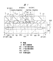
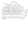
本実施の形態の半導体装置を、図面を参照して説明する。図1は、本実施の形態の半導体装置の要部断面図であり、図2および図3は、本実施の形態の半導体装置の要部平面図である。図2と図3とは、同じ平面領域が示されている。理解を簡単にするために、図2では、p+型半導体領域PR1、n+型半導体領域NR1、n+型半導体領域NR2および電極FPに細線の斜線のハッチングを付し、図3では、p+型半導体領域PR1、n+型半導体領域NR1およびn+型半導体領域NR2に細線の斜線のハッチングを付し、素子分離領域LSに太線の斜線のハッチングを付してある。また、図3では、素子分離領域LSに形成された溝TRの位置を点線で示してある。図2および図3のA−A線の断面図が、図1にほぼ対応している。
(Embodiment 1)
<Structure of semiconductor device>
The semiconductor device of the present embodiment will be described with reference to the drawings. FIG. 1 is a cross-sectional view of main parts of the semiconductor device of the present embodiment, and FIGS. 2 and 3 are plan views of main parts of the semiconductor device of the present embodiment. 2 and 3 show the same planar area. For easy understanding, in FIG. 2, the p + type semiconductor region PR1, the n + type semiconductor region NR1, the n + type semiconductor region NR2, and the electrode FP are hatched with thin diagonal lines, and in FIG. The + type semiconductor region PR1, the n + type semiconductor region NR1 and the n + type semiconductor region NR2 are hatched with thin hatched lines, and the element isolation region LS is hatched with thick hatched lines. In FIG. 3, the position of the trench TR formed in the element isolation region LS is indicated by a dotted line. A cross-sectional view taken along line AA in FIGS. 2 and 3 substantially corresponds to FIG.
本実施の形態の半導体装置は、バイポーラトランジスタを有する半導体装置である。 The semiconductor device of this embodiment is a semiconductor device having a bipolar transistor.
以下、本実施の形態の半導体装置の構造について、図1〜図3を参照して具体的に説明する。 Hereinafter, the structure of the semiconductor device of this embodiment will be specifically described with reference to FIGS.
図1〜図3に示されるように、バイポーラトランジスタが、半導体基板SUBの主面に形成されている。 As shown in FIGS. 1 to 3, the bipolar transistor is formed on the main surface of the semiconductor substrate SUB.
半導体基板SUBは、例えばホウ素(B)などのp型不純物が導入されたp型の単結晶シリコンなどからなる半導体基板である基板本体SBと、基板本体SBの主面上に形成された、p−型の単結晶シリコンなどからなるエピタキシャル層(半導体層、エピタキシャル半導体層)EPとを有している。このため、半導体基板SUBは、いわゆるエピタキシャルウエハである。基板本体SBとエピタキシャル層EPとは、同じ導電型(ここではp型)であるが、基板本体SBの不純物濃度(p型不純物濃度)は、エピタキシャル層EPの不純物濃度(p型不純物濃度)よりも高くなっており、基板本体SBの抵抗率(比抵抗)は、エピタキシャル層EPの抵抗率(比抵抗)よりも低い。 The semiconductor substrate SUB includes, for example, a substrate body SB that is a semiconductor substrate made of p-type single crystal silicon into which a p-type impurity such as boron (B) is introduced, and a p-type substrate formed on the main surface of the substrate body SB. And an epitaxial layer (semiconductor layer, epitaxial semiconductor layer) EP made of -type single crystal silicon or the like. For this reason, the semiconductor substrate SUB is a so-called epitaxial wafer. The substrate body SB and the epitaxial layer EP have the same conductivity type (here, p-type), but the impurity concentration (p-type impurity concentration) of the substrate body SB is greater than the impurity concentration (p-type impurity concentration) of the epitaxial layer EP. The resistivity (specific resistance) of the substrate body SB is lower than the resistivity (specific resistance) of the epitaxial layer EP.
ここで、エピタキシャル層EPのうち、p−型の状態が維持されている領域を、p−型エピタキシャル層EP1と称することとする。エピタキシャル層EP内には、n+型埋込領域NBの上部、n型ウエルNW1、p型ウエルPW1、n+型半導体領域NR1、p+型半導体領域PR1、n+型半導体領域NR2およびn+型シンカー領域NSが形成されているが、それらを除く領域が、p−型エピタキシャル層EP1に対応している。このため、p−型エピタキシャル層EP1は、基板本体SBと同じ導電型(ここではp型)であるが、p−型エピタキシャル層EP1の不純物濃度(p型不純物濃度)は、基板本体SBの不純物濃度(p型不純物濃度)よりも低く、p−型エピタキシャル層EP1の抵抗率は、基板本体SBの抵抗率よりも高い。 Here, a region in the epitaxial layer EP in which the p − type state is maintained is referred to as a p − type epitaxial layer EP1. In the epitaxial layer EP, the upper part of the n + type buried region NB, the n type well NW1, the p type well PW1, the n + type semiconductor region NR1, the p + type semiconductor region PR1, the n + type semiconductor region NR2 and the n + The type sinker region NS is formed, but the region excluding them corresponds to the p − type epitaxial layer EP1. Therefore, the p − type epitaxial layer EP1 has the same conductivity type as the substrate body SB (here, p type), but the impurity concentration (p type impurity concentration) of the p − type epitaxial layer EP1 is the impurity of the substrate body SB. Lower than the concentration (p-type impurity concentration), the resistivity of the p − -type epitaxial layer EP1 is higher than the resistivity of the substrate body SB.
半導体基板SUBの主面(上面)には、絶縁膜からなる素子分離領域(素子分離絶縁膜、フィールド絶縁膜)LSが形成されている。素子分離領域LSは、素子分離絶縁膜とみなすことができる。ここでは、素子分離領域LSとして、LOCOS法により形成されたLOCOS酸化膜を形成した場合が示されているが、他の形態として、素子分離領域LSとして、STI法により形成したSTI絶縁膜を用いることもできる。 An element isolation region (element isolation insulating film, field insulating film) LS made of an insulating film is formed on the main surface (upper surface) of the semiconductor substrate SUB. The element isolation region LS can be regarded as an element isolation insulating film. Here, a case where a LOCOS oxide film formed by the LOCOS method is formed as the element isolation region LS is shown, but as another embodiment, an STI insulating film formed by the STI method is used as the element isolation region LS. You can also
ここで、LOCOS酸化膜(LOCOS分離膜)とは、LOCOS(Local oxidation of silicon)法により形成された酸化膜(酸化シリコン膜)である。LOCOS法とは、半導体基板の主面上に耐酸化膜(例えば窒化シリコン膜)を形成してから、半導体基板を熱酸化することにより、耐酸化膜で覆われていない領域の半導体基板の主面に、熱酸化膜(LOCOS酸化膜)を選択的(局所的)に形成する手法であり、形成された熱酸化膜がLOCOS酸化膜(LOCOS分離膜)である。 Here, the LOCOS oxide film (LOCOS isolation film) is an oxide film (silicon oxide film) formed by a LOCOS (Local oxidation of silicon) method. In the LOCOS method, an oxide-resistant film (for example, a silicon nitride film) is formed on the main surface of the semiconductor substrate, and then the semiconductor substrate is thermally oxidized, whereby the main region of the semiconductor substrate that is not covered with the oxide-resistant film is formed. In this method, a thermal oxide film (LOCOS oxide film) is selectively (locally) formed on the surface, and the formed thermal oxide film is a LOCOS oxide film (LOCOS isolation film).
また、STI絶縁膜(STI分離膜)は、STI(Shallow Trench Isolation)法により形成された絶縁膜である。STI法とは、半導体基板の主面に溝を形成してから、その溝に絶縁膜を埋め込む手法であり、その溝に埋め込まれた絶縁膜が、STI絶縁膜(STI分離膜)である。 The STI insulating film (STI isolation film) is an insulating film formed by an STI (Shallow Trench Isolation) method. The STI method is a technique in which a groove is formed in the main surface of a semiconductor substrate and then an insulating film is embedded in the groove. The insulating film embedded in the groove is an STI insulating film (STI isolation film).
半導体基板SUBにおいて、基板本体SBとエピタキシャル層EPとの間には、n型不純物が高濃度に導入(ドープ)されたn+型埋込領域NBが形成されている。n+型埋込領域NBは、n型不純物が高濃度に導入されたn+型の半導体領域である。 In the semiconductor substrate SUB, an n + type buried region NB into which an n type impurity is introduced (doped) at a high concentration is formed between the substrate body SB and the epitaxial layer EP. The n + type buried region NB is an n + type semiconductor region into which an n type impurity is introduced at a high concentration.
エピタキシャル層EP内には、n型ウエルNW1が形成され、n型ウエルNW1内に、p型ウエルPW1が形成され、p型ウエルPW1内にn+型半導体領域NR1およびp+型半導体領域PR1が形成されている。 An n-type well NW1 is formed in the epitaxial layer EP, a p-type well PW1 is formed in the n-type well NW1, and an n + -type semiconductor region NR1 and a p + -type semiconductor region PR1 are formed in the p-type well PW1. Is formed.
n型ウエルNW1は、n+型埋込領域NB上に形成されており、n型ウエルNW1の底面(下面)は、n+型埋込領域NBに接している。n型ウエルNW1の側面は、p−型エピタキシャル層EP1に接している。また、n型ウエルNW1の側面は、素子分離領域LSの下に位置している。n型ウエルNW1は、n型の半導体領域である。 The n-type well NW1 is formed on the n + -type buried region NB, and the bottom surface (lower surface) of the n-type well NW1 is in contact with the n + -type buried region NB. The side surface of the n-type well NW1 is in contact with the p − -type epitaxial layer EP1. The side surface of the n-type well NW1 is located below the element isolation region LS. The n-type well NW1 is an n-type semiconductor region.
p型ウエルPW1は、n型ウエルNW1に内包されるように形成されている。このため、p型ウエルPW1の底面(下面)および側面は、n型ウエルNW1に接している。また、p型ウエルPW1の側面は、素子分離領域LSの下に位置している。p型ウエルPW1は、p型の半導体領域である。 The p-type well PW1 is formed so as to be enclosed in the n-type well NW1. For this reason, the bottom surface (lower surface) and the side surface of the p-type well PW1 are in contact with the n-type well NW1. The side surface of the p-type well PW1 is located below the element isolation region LS. The p-type well PW1 is a p-type semiconductor region.
n+型半導体領域NR1は、p型ウエルPW1に内包されるように形成されている。このため、n+型半導体領域NR1の底面(下面)および側面は、p型ウエルPW1に接している。n+型半導体領域NR1は、n型ウエルNW1には接しておらず、n+型半導体領域NR1とn型ウエルNW1との間には、p型ウエルPW1の一部が介在している。 The n + type semiconductor region NR1 is formed so as to be enclosed in the p type well PW1. For this reason, the bottom surface (lower surface) and side surface of the n + type semiconductor region NR1 are in contact with the p type well PW1. The n + type semiconductor region NR1 is not in contact with the n type well NW1, and a part of the p type well PW1 is interposed between the n + type semiconductor region NR1 and the n type well NW1.
p+型半導体領域PR1は、p型ウエルPW1に内包されるように形成されている。このため、p+型半導体領域PR1の底面(下面)および側面は、p型ウエルPW1に接している。p+型半導体領域PR1は、n型ウエルNW1には接しておらず、p+型半導体領域PR1とn型ウエルNW1との間には、p型ウエルPW1の一部が介在している。また、p型ウエルPW1内にn+型半導体領域NR1とp+型半導体領域PR1とが形成されているが、p+型半導体領域PR1とn+型半導体領域NR1とは、互いに接しておらず、離間して形成されている。 The p + type semiconductor region PR1 is formed so as to be enclosed in the p type well PW1. Therefore, the bottom surface (lower surface) and the side surface of the p + type semiconductor region PR1 are in contact with the p type well PW1. The p + type semiconductor region PR1 is not in contact with the n type well NW1, and a part of the p type well PW1 is interposed between the p + type semiconductor region PR1 and the n type well NW1. Further, the n + type semiconductor region NR1 and the p + type semiconductor region PR1 are formed in the p type well PW1, but the p + type semiconductor region PR1 and the n + type semiconductor region NR1 are not in contact with each other. , Spaced apart.
n+型半導体領域NR1およびp+型半導体領域PR1は、エピタキシャル層EPの表層部に形成されており、従って半導体基板SUBの表層部に形成されている。このため、n+型半導体領域NR1の上面とp+型半導体領域PR1の上面とは、エピタキシャル層EPの上面(半導体基板SUBの上面)と一致している。n+型半導体領域NR1上と、p+型半導体領域PR1上とには、素子分離領域LSは形成されておらず、平面視において、n+型半導体領域NR1は、周囲を素子分離領域LSによって囲まれており、また、p+型半導体領域PR1も、周囲を素子分離領域LSによって囲まれている。すなわち、n+型半導体領域NR1上とp+型半導体領域PR1と後述のn+型半導体領域NR2とは、それぞれ、半導体基板SUBの主面において、素子分離領域LSに周囲を囲まれた活性領域(素子分離領域LSが形成されていない領域)に形成されている。 The n + type semiconductor region NR1 and the p + type semiconductor region PR1 are formed in the surface layer portion of the epitaxial layer EP, and thus are formed in the surface layer portion of the semiconductor substrate SUB. For this reason, the upper surface of the n + type semiconductor region NR1 and the upper surface of the p + type semiconductor region PR1 coincide with the upper surface of the epitaxial layer EP (the upper surface of the semiconductor substrate SUB). The element isolation region LS is not formed on the n + type semiconductor region NR1 and the p + type semiconductor region PR1, and the n + type semiconductor region NR1 is surrounded by the element isolation region LS in plan view. The p + type semiconductor region PR1 is also surrounded by the element isolation region LS. That is, the n + -type semiconductor region NR1, the p + -type semiconductor region PR1, and the n + -type semiconductor region NR2 described later are each an active region surrounded by the element isolation region LS on the main surface of the semiconductor substrate SUB. (A region where the element isolation region LS is not formed).
ここで、「平面視」とは、半導体基板SUBの主面に平行な平面で見た場合に対応している。 Here, the “plan view” corresponds to the case of viewing in a plane parallel to the main surface of the semiconductor substrate SUB.
n型ウエルNW1内には、更に、n+型半導体領域NR2およびn+型シンカー領域NSも形成されている。n+型半導体領域NR2は、エピタキシャル層EPの表層部に形成されており、従って半導体基板SUBの表層部に形成されている。このため、n+型半導体領域NR2の上面は、エピタキシャル層EPの上面(半導体基板SUBの上面)と一致している。n+型半導体領域NR2上には素子分離領域LSは形成されておらず、平面視において、n+型半導体領域NR2は、周囲を素子分離領域LSによって囲まれている。 In the n-type well NW1, an n + type semiconductor region NR2 and an n + type sinker region NS are further formed. The n + type semiconductor region NR2 is formed in the surface layer portion of the epitaxial layer EP, and thus is formed in the surface layer portion of the semiconductor substrate SUB. For this reason, the upper surface of the n + -type semiconductor region NR2 coincides with the upper surface of the epitaxial layer EP (the upper surface of the semiconductor substrate SUB). n + -type semiconductor region isolation region LS is on NR2 is not formed, in plan view, the n + -type semiconductor region NR2 are surrounded by the isolation region LS.
また、平面視において、n+型半導体領域NR1とn+型半導体領域NR2との間にp+型半導体領域PR1が配置されている。このため、平面視において、n+型半導体領域NR1とp+型半導体領域PR1との間には、素子分離領域LSが介在し、p+型半導体領域PR1とn+型半導体領域NR2との間にも、素子分離領域LSが介在している。 Further, in plan view, the p + type semiconductor region PR1 is disposed between the n + type semiconductor region NR1 and the n + type semiconductor region NR2. For this reason, in plan view, the element isolation region LS is interposed between the n + type semiconductor region NR1 and the p + type semiconductor region PR1, and between the p + type semiconductor region PR1 and the n + type semiconductor region NR2. In addition, the element isolation region LS is interposed.
n+型シンカー領域NSは、n+型埋込領域NBに達するように、形成されている。このため、n+型シンカー領域NSの底面(下面)は、n+型埋込領域NBに接している。n+型シンカー領域NSの側面は、n型ウエルNW1内に接している。n+型半導体領域NR2は、n+型シンカー領域NSに内包されるように形成されている。このため、n+型半導体領域NR2の底面(下面)および側面は、n+型シンカー領域NSに接している。n+型半導体領域NR2とn+型埋込領域NBとの間には、n+型シンカー領域NSが介在している。また、n+型シンカー領域NSとp型ウエルPW1とは接しておらず、n+型シンカー領域NSとp型ウエルPW1との間には、n型ウエルNW1の一部が介在している。n+型シンカー領域NSは、n型不純物が高濃度に導入されたn+型の半導体領域である。 The n + type sinker region NS is formed so as to reach the n + type buried region NB. For this reason, the bottom surface (lower surface) of the n + type sinker region NS is in contact with the n + type buried region NB. The side surface of the n + type sinker region NS is in contact with the n type well NW1. The n + type semiconductor region NR2 is formed so as to be included in the n + type sinker region NS. For this reason, the bottom surface (lower surface) and side surface of the n + type semiconductor region NR2 are in contact with the n + type sinker region NS. An n + type sinker region NS is interposed between the n + type semiconductor region NR2 and the n + type buried region NB. Further, the n + type sinker region NS and the p type well PW1 are not in contact with each other, and a part of the n type well NW1 is interposed between the n + type sinker region NS and the p type well PW1. The n + type sinker region NS is an n + type semiconductor region into which an n type impurity is introduced at a high concentration.
n+型半導体領域NR2とn+型シンカー領域NSとn+型埋込領域NBとが連続的に繋がった状態になっている。n+型半導体領域NR2とn+型シンカー領域NSとn+型埋込領域NBとは、いずれもn型ウエルNW1よりも不純物濃度が高い。このため、n+型半導体領域NR2は、n+型シンカー領域NSを介してn+型埋込領域NBに、低抵抗で電気的に接続された状態になっている。 The n + type semiconductor region NR2, the n + type sinker region NS, and the n + type buried region NB are continuously connected. The n + type semiconductor region NR2, the n + type sinker region NS, and the n + type buried region NB all have an impurity concentration higher than that of the n type well NW1. Therefore, the n + type semiconductor region NR2 is in a state of being electrically connected to the n + type buried region NB through the n + type sinker region NS with a low resistance.
n+型半導体領域NR1とp+型半導体領域PR1とn+型半導体領域NR2とは、互いに離間しており、平面視において、n+型半導体領域NR1とn+型半導体領域NR2との間にp+型半導体領域PR1が形成されている。このため、n+型半導体領域NR1とp+型半導体領域PR1とn+型半導体領域NR2とは、互いに接していない。n+型半導体領域NR1とp+型半導体領域PR1との間には、素子分離領域LSが存在し、n+型半導体領域NR2とp+型半導体領域PR1との間にも、素子分離領域LSが存在している。 The n + type semiconductor region NR1, the p + type semiconductor region PR1, and the n + type semiconductor region NR2 are separated from each other, and are between the n + type semiconductor region NR1 and the n + type semiconductor region NR2 in plan view. A p + type semiconductor region PR1 is formed. For this reason, the n + type semiconductor region NR1, the p + type semiconductor region PR1, and the n + type semiconductor region NR2 are not in contact with each other. An element isolation region LS exists between the n + type semiconductor region NR1 and the p + type semiconductor region PR1, and the element isolation region LS is also provided between the n + type semiconductor region NR2 and the p + type semiconductor region PR1. Is present.
また、n+型半導体領域NR1とp+型半導体領域PR1との間に介在する素子分離領域LSの直下には、p型ウエルPW1が存在している。すなわち、n+型半導体領域NR1とp+型半導体領域PR1との間に位置する素子分離領域LSの下には、p型ウエルPW1が延在している。このため、n+型半導体領域NR1とp+型半導体領域PR1との間に位置する素子分離領域LSの下面は、p型ウエルPW1に接している。従って、n+型半導体領域NR1とp+型半導体領域PR1との間には、p型ウエルPW1の一部が介在している。 In addition, a p-type well PW1 exists immediately below the element isolation region LS interposed between the n + -type semiconductor region NR1 and the p + -type semiconductor region PR1. That is, the p-type well PW1 extends under the element isolation region LS located between the n + -type semiconductor region NR1 and the p + -type semiconductor region PR1. For this reason, the lower surface of the element isolation region LS located between the n + type semiconductor region NR1 and the p + type semiconductor region PR1 is in contact with the p type well PW1. Accordingly, a part of the p-type well PW1 is interposed between the n + type semiconductor region NR1 and the p + type semiconductor region PR1.
また、n+型半導体領域NR2とp+型半導体領域PR1との間に介在する素子分離領域LSの直下には、n型ウエルNW1の一部とp型ウエルPW1の一部とが存在しており、素子分離領域LSの直下の領域は、n+型半導体領域NR2側がn型ウエルNW1であり、p+型半導体領域PR1側がp型ウエルPW1になっている。このため、n+型半導体領域NR2とp+型半導体領域PR1との間には、n型ウエルNW1の一部とp型ウエルPW1の一部とが介在し、n+型半導体領域NR2側がn型ウエルNW1であり、p+型半導体領域PR1側がp型ウエルPW1になっている。 Further, a part of the n-type well NW1 and a part of the p-type well PW1 exist immediately below the element isolation region LS interposed between the n + -type semiconductor region NR2 and the p + -type semiconductor region PR1. In the region immediately below the element isolation region LS, the n + type semiconductor region NR2 side is the n type well NW1, and the p + type semiconductor region PR1 side is the p type well PW1. Therefore, a part of the n-type well NW1 and a part of the p-type well PW1 are interposed between the n + -type semiconductor region NR2 and the p + -type semiconductor region PR1, and the n + -type semiconductor region NR2 side is n This is the type well NW1, and the p + type semiconductor region PR1 side is the p type well PW1.
n+型半導体領域NR2がn型ウエルNW1と接触せずに、n+型半導体領域NR2とn型ウエルNW1との間にn+型シンカー領域NSの一部が介在する場合は、そのn+型半導体領域NR2とn型ウエルNW1との間に介在する部分のn+型シンカー領域NSと、n型ウエルNW1の一部と、p型ウエルPW1の一部とが、n+型半導体領域NR2とp+型半導体領域PR1との間に介在する。 When the n + type semiconductor region NR2 is not in contact with the n type well NW1 and a part of the n + type sinker region NS is interposed between the n + type semiconductor region NR2 and the n type well NW1, the n + A portion of n + type sinker region NS interposed between n type semiconductor region NR2 and n type well NW1, a portion of n type well NW1, and a portion of p type well PW1 are n + type semiconductor region NR2 And p + type semiconductor region PR1.
n+型埋込領域NBは、基板本体SBとエピタキシャル層EPとの界面付近に、基板本体SBとエピタキシャル層EPとにわたって形成されている。このため、n+型埋込領域NBの下部は、基板本体SBに形成され、n+型埋込領域NBの上部は、エピタキシャル層EPに形成されている。 The n + type buried region NB is formed across the substrate body SB and the epitaxial layer EP in the vicinity of the interface between the substrate body SB and the epitaxial layer EP. Therefore, the lower part of the n + type buried region NB is formed in the substrate body SB, and the upper part of the n + type buried region NB is formed in the epitaxial layer EP.
n+型埋込領域NBの底面(下面)は、p型となっている基板本体SBに接している。n+型埋込領域NBの上面は、主としてn型ウエルNW1の底面に接しているが、n型ウエルNW1内に形成されたn+型シンカー領域NSの底面にも接している。n型ウエルNW1が形成されていない領域では、n+型埋込領域NBの上面はp−型エピタキシャル層EP1に接している。n+型埋込領域NBの側面のうち、下部はp型となっている基板本体SBに接し、上部はp−型エピタキシャル層EP1に接している。 The bottom surface (lower surface) of the n + type buried region NB is in contact with the p-type substrate body SB. The upper surface of the n + type buried region NB is mainly in contact with the bottom surface of the n type well NW1, but is also in contact with the bottom surface of the n + type sinker region NS formed in the n type well NW1. In the region where the n-type well NW1 is not formed, the upper surface of the n + -type buried region NB is in contact with the p − -type epitaxial layer EP1. Of the side surfaces of the n + -type buried region NB, the lower portion is in contact with the p-type substrate body SB and the upper portion is in contact with the p − -type epitaxial layer EP1.
n+型半導体領域NR1とp+型半導体領域PR1との間に介在する素子分離領域LSには、溝TRが形成されており、溝TR内を含む素子分離領域LS上に電極FPが形成されている。溝TR内は、電極FPによって埋め込まれている。平面視において、溝TRは電極FPに内包されている。電極FPは、溝TR内を埋める部分と、溝TRの外部で素子分離領域LS上に位置する(延在する)部分とを一体的に有している。電極FPにプラグPGFを接続できるのであれば、電極FPは、溝TRの外部で素子分離領域LS上に位置する(延在する)部分を有さない場合もあり得る。電極FPは、フィールドプレート電極とみなすこともできる。 A trench TR is formed in the element isolation region LS interposed between the n + type semiconductor region NR1 and the p + type semiconductor region PR1, and an electrode FP is formed on the element isolation region LS including the inside of the trench TR. ing. The inside of the trench TR is filled with the electrode FP. In a plan view, the trench TR is included in the electrode FP. The electrode FP integrally includes a portion that fills the trench TR and a portion that is located (extends) on the element isolation region LS outside the trench TR. If the plug PGF can be connected to the electrode FP, the electrode FP may not have a portion located (extended) on the element isolation region LS outside the trench TR. The electrode FP can also be regarded as a field plate electrode.
平面視において、溝TRは、n+型半導体領域NR1とp+型半導体領域PR1との間に配置されている。このため、平面視において、電極FPは、n+型半導体領域NR1とp+型半導体領域PR1との間に配置されている。電極FPの直下には素子分離領域LSが存在している。溝TRの直下での素子分離領域LSの厚みは、溝TRの外部での素子分離領域LSの厚みよりも、小さく(薄く)なっている。このため、溝TR内に埋め込まれた部分の電極FPの直下における素子分離領域LSの厚みは、溝TRの外部に位置する部分の電極FPの直下における素子分離領域LSの厚みよりも、小さく(薄く)なっている。電極FPの直下には、素子分離領域LSがあり、更にその直下には、p型ウエルPW1があるため、上下方向に見ると、電極FPは、素子分離領域LS(電極FPの直下に位置する部分の素子分離領域LS)を介して、p型ウエルPW1と対向している。 In plan view, the trench TR is disposed between the n + type semiconductor region NR1 and the p + type semiconductor region PR1. For this reason, the electrode FP is disposed between the n + type semiconductor region NR1 and the p + type semiconductor region PR1 in plan view. An element isolation region LS exists immediately below the electrode FP. The thickness of the element isolation region LS immediately below the trench TR is smaller (thinner) than the thickness of the element isolation region LS outside the trench TR. For this reason, the thickness of the element isolation region LS directly under the electrode FP in the portion embedded in the trench TR is smaller than the thickness of the element isolation region LS immediately under the electrode FP in the portion located outside the trench TR ( Thin). Since there is an element isolation region LS immediately below the electrode FP, and there is a p-type well PW1 immediately below it, the electrode FP is located in the element isolation region LS (directly below the electrode FP) when viewed in the vertical direction. The p-type well PW1 is opposed to the element isolation region LS).
電極FPは、導電膜からなり、例えば不純物(リン、ホウ素またはヒ素など)を導入したポリシリコン膜(ドープトポリシリコン膜)からなる。他の形態として、電極FPを構成する材料として、アルミニウム(Al)、銅(Cu)またはタングステン(W)などの金属材料を用いることもできる。 The electrode FP is made of a conductive film, for example, a polysilicon film (doped polysilicon film) into which impurities (phosphorus, boron, arsenic, etc.) are introduced. As another form, a metal material such as aluminum (Al), copper (Cu), or tungsten (W) can be used as a material constituting the electrode FP.
半導体基板SUBの主面(上面)上には、素子分離領域LSおよび電極FPを覆うように、絶縁膜として層間絶縁膜ILが形成されている。層間絶縁膜ILは、例えば酸化シリコン膜などからなる。層間絶縁膜ILの上面は平坦化されている。層間絶縁膜ILとして、積層絶縁膜を用いることも可能であり、例えば、窒化シリコン膜と該窒化シリコン膜上の酸化シリコン膜との積層膜を層間絶縁膜ILとして用いることもでき、その場合、窒化シリコン膜よりも酸化シリコン膜を厚くすることが好ましい。なお、積層絶縁膜とは、複数の絶縁膜からなる積層膜のことである。 On the main surface (upper surface) of the semiconductor substrate SUB, an interlayer insulating film IL is formed as an insulating film so as to cover the element isolation region LS and the electrode FP. The interlayer insulating film IL is made of, for example, a silicon oxide film. The upper surface of the interlayer insulating film IL is planarized. A laminated insulating film can also be used as the interlayer insulating film IL. For example, a laminated film of a silicon nitride film and a silicon oxide film on the silicon nitride film can be used as the interlayer insulating film IL. It is preferable to make the silicon oxide film thicker than the silicon nitride film. Note that the laminated insulating film is a laminated film including a plurality of insulating films.
層間絶縁膜ILには、コンタクトホール(開口部、スルーホール、貫通孔)が形成され、コンタクトホール内には、例えばタングステン(W)膜を主体とする導電性のプラグ(接続用埋込導体、コンタクトプラグ)PGが形成されている。すなわち、導電性のプラグPGが、層間絶縁膜ILに形成されたコンタクトホールに埋め込まれている。プラグPGは、接続用のプラグであり、すなわちコンタクトプラグである。プラグPGは、複数形成されており、エミッタ用プラグPGE、ベース用プラグPGB、コレクタ用プラグPGC、およびプラグPGFを有している。 In the interlayer insulating film IL, contact holes (openings, through-holes, through-holes) are formed, and in the contact holes, for example, conductive plugs mainly composed of a tungsten (W) film (connection embedded conductors, A contact plug) PG is formed. That is, the conductive plug PG is embedded in the contact hole formed in the interlayer insulating film IL. The plug PG is a connection plug, that is, a contact plug. A plurality of plugs PG are formed, and include an emitter plug PGE, a base plug PGB, a collector plug PGC, and a plug PGF.
ここで、プラグPGのうち、エミッタ用のn+型半導体領域NR1上に配置されてそのエミッタ用のn+型半導体領域NR1に電気的に接続されたプラグPGを、エミッタ用プラグPGEと称することとする。また、プラグPGのうち、ベース用のp+型半導体領域PR1上に配置されてそのベース用のp+型半導体領域PR1に電気的に接続されたプラグPGを、ベース用プラグPGBと称することとする。また、プラグPGのうち、コレクタ用のn+型半導体領域NR2上に配置されてそのコレクタ用のn+型半導体領域NR2に電気的に接続されたプラグPGを、コレクタ用プラグPGCと称することとする。また、プラグPGのうち、電極FP上に配置されてその電極FPに電気的に接続されたプラグPGを、プラグPGFと称することとする。 Here, among the plugs PG, is disposed on n + -type semiconductor region NR1 for emitter n + -type semiconductor region NR1 for its emitter electrically connected to the plug PG, be referred to as emitter plug PGE And Also, among the plugs PG, to the p + -type semiconductor region for the base are disposed on the PR1 p + -type semiconductor region PR1 electrically connected to plug PG for the base, referred to as the base plug PGB and To do. Also, among the plugs PG, the n + -type semiconductor region disposed on the NR2 and n + -type electrically connected to the semiconductor region NR2 have been plugs PG for the collector for the collector, and be referred to as a collector plug PGC To do. Of the plugs PG, the plug PG disposed on the electrode FP and electrically connected to the electrode FP is referred to as a plug PGF.
エミッタ用プラグPGEは、その底面がn+型半導体領域NR1に接することにより、n+型半導体領域NR1と電気的に接続されている。n+型半導体領域NR1上に金属シリサイド層を形成した場合は、エミッタ用プラグPGEは、n+型半導体領域NR1上の金属シリサイド層に接し、その金属シリサイド層を介してn+型半導体領域NR1と電気的に接続される。 The emitter plug PGE is electrically connected to the n + type semiconductor region NR1 by contacting the bottom surface of the emitter plug PGE with the n + type semiconductor region NR1. When forming a metal silicide layer on the n + -type semiconductor region NR1, the emitter plug PGE is, n + -type semiconductor region in contact with the metal silicide layer on NR1, through the metal silicide layer n + -type semiconductor region NR1 And electrically connected.
ベース用プラグPGBは、その底面がp+型半導体領域PR1に接することにより、p+型半導体領域PR1と電気的に接続されている。p+型半導体領域PR1上に金属シリサイド層を形成した場合は、ベース用プラグPGBは、p+型半導体領域PR1上の金属シリサイド層に接し、その金属シリサイド層を介してp+型半導体領域PR1と電気的に接続される。 Bass plug PGB has its bottom by contact with the p + -type semiconductor region PR1, p + -type semiconductor region PR1 and are electrically connected. When forming a metal silicide layer on the p + -type semiconductor region PR1, base plug PGB is, p + -type semiconductor region in contact with the metal silicide layer on PR1, p + -type semiconductor region PR1 through the metal silicide layer And electrically connected.
コレクタ用プラグPGCは、その底面がn+型半導体領域NR2に接することにより、n+型半導体領域NR2と電気的に接続されている。n+型半導体領域NR2上に金属シリサイド層を形成した場合は、コレクタ用プラグPGCは、n+型半導体領域NR2上の金属シリサイド層に接し、その金属シリサイド層を介してn+型半導体領域NR2と電気的に接続される。 The collector plug PGC is electrically connected to the n + type semiconductor region NR2 by contacting the bottom surface of the collector plug PGC with the n + type semiconductor region NR2. n + -type semiconductor when an area forming a metal silicide layer over NR2, collector plug PGC is, n + -type semiconductor region in contact with the metal silicide layer on the NR2, n + -type semiconductor region NR2 through the metal silicide layer And electrically connected.
プラグPGFは、その底面が電極FPに接することにより、電極FPと電気的に接続されている。電極FP上に金属シリサイド層を形成した場合は、プラグPGFは、電極FP上の金属シリサイド層に接し、その金属シリサイド層を介して電極FPと電気的に接続される。 The plug PGF is electrically connected to the electrode FP by contacting the bottom surface of the plug PGF with the electrode FP. When the metal silicide layer is formed on the electrode FP, the plug PGF is in contact with the metal silicide layer on the electrode FP and is electrically connected to the electrode FP via the metal silicide layer.
プラグPGが埋め込まれた層間絶縁膜IL上には、配線(第1層配線)M1が形成されている。 On the interlayer insulating film IL in which the plug PG is embedded, a wiring (first layer wiring) M1 is formed.
配線M1は、例えば、プラグPGが埋め込まれた層間絶縁膜IL上に導電膜を形成してから、その導電膜をパターニングすることにより形成されており、その場合は、配線M1は、パターニングされた導電膜からなる。配線M1としては、例えばアルミニウム配線などを好適に用いることができる。他の形態として、配線M1として、ダマシン法で形成したダマシン配線(埋込配線)を用いることも可能である。層間絶縁膜ILおよび配線M1よりも上層に、更に層間絶縁膜および配線が形成されているが、ここではその図示および説明は省略する。 The wiring M1 is formed, for example, by forming a conductive film on the interlayer insulating film IL in which the plug PG is embedded and then patterning the conductive film. In that case, the wiring M1 is patterned. It consists of a conductive film. As the wiring M1, for example, an aluminum wiring can be preferably used. As another form, a damascene wiring (embedded wiring) formed by a damascene method can be used as the wiring M1. Although an interlayer insulating film and a wiring are further formed above the interlayer insulating film IL and the wiring M1, illustration and description thereof are omitted here.
ここで、配線M1のうち、プラグPG(より特定的にはエミッタ用プラグPGE)を介してエミッタ用のn+型半導体領域NR1に電気的に接続された配線M1を、エミッタ用配線M1Eと称することとする。なお、エミッタ用配線M1Eは、エミッタ用プラグPGEを介してエミッタ用のn+型半導体領域NR1と電気的に接続されるとともに、プラグPGFを介して電極FPと電気的に接続されている。また、配線M1のうち、プラグPG(より特定的にはベース用プラグPGB)を介してベース用のp+型半導体領域PR1に電気的に接続された配線M1を、ベース用配線M1Bと称することとする。また、配線M1のうち、プラグPG(より特定的にはコレクタ用プラグPGC)を介してコレクタ用のn+型半導体領域NR2に電気的に接続された配線M1を、コレクタ用配線M1Cと称することとする。エミッタ用配線M1Eとベース用配線M1Bとコレクタ用配線M1Cとは、互いに分離されている。すなわち、エミッタ用配線M1Eとベース用配線M1Bとは、導体を通じて接続されておらず、かつ、エミッタ用配線M1Eとコレクタ用配線M1Cとは、導体を通じて接続されておらず、かつ、ベース用配線M1Bとコレクタ用配線M1Cとは、導体を通じて接続されていない。 Here, of the wiring M1, the wiring M1 electrically connected to the emitter n + -type semiconductor region NR1 via the plug PG (more specifically, the emitter plug PGE) is referred to as an emitter wiring M1E. I will do it. The emitter wiring M1E is electrically connected to the emitter n + -type semiconductor region NR1 via the emitter plug PGE and electrically connected to the electrode FP via the plug PGF. Of the wiring M1, the wiring M1 electrically connected to the base p + type semiconductor region PR1 via the plug PG (more specifically, the base plug PGB) is referred to as a base wiring M1B. And Of the wiring M1, the wiring M1 electrically connected to the collector n + type semiconductor region NR2 via the plug PG (more specifically, the collector plug PGC) is referred to as a collector wiring M1C. And The emitter wiring M1E, the base wiring M1B, and the collector wiring M1C are separated from each other. That is, the emitter wiring M1E and the base wiring M1B are not connected through the conductor, and the emitter wiring M1E and the collector wiring M1C are not connected through the conductor, and the base wiring M1B. And the collector wiring M1C are not connected through a conductor.
ベース用配線M1Bは、ベース用プラグPGB上を含む層間絶縁膜ILに延在し、ベース用プラグPGBと平面視において重なっており、ベース用プラグPGBの上面がベース用配線M1Bと接することで、ベース用プラグPGBとベース用配線M1Bとが電気的に接続されている。 The base wiring M1B extends to the interlayer insulating film IL including the base plug PGB and overlaps the base plug PGB in a plan view, and the upper surface of the base plug PGB is in contact with the base wiring M1B. The base plug PGB and the base wiring M1B are electrically connected.
コレクタ用配線M1Cは、コレクタ用プラグPGC上を含む層間絶縁膜ILに延在し、コレクタ用プラグPGCと平面視において重なっており、コレクタ用プラグPGCの上面がコレクタ用配線M1Cと接することで、コレクタ用プラグPGCとコレクタ用配線M1Cとが電気的に接続されている。 The collector wiring M1C extends to the interlayer insulating film IL including the collector plug PGC and overlaps with the collector plug PGC in plan view, and the upper surface of the collector plug PGC is in contact with the collector wiring M1C. The collector plug PGC and the collector wiring M1C are electrically connected.
ベース用配線M1Bからベース用プラグPGBを介してベース用のp+型半導体領域PR1に所望のベース電圧を供給することができる。また、コレクタ用配線M1Cからコレクタ用プラグPGCを介してコレクタ用のn+型半導体領域NR2に所望のコレクタ電圧を供給することができる。 A desired base voltage can be supplied from the base wiring M1B to the base p + type semiconductor region PR1 via the base plug PGB. Further, a desired collector voltage can be supplied from the collector wiring M1C to the collector n + type semiconductor region NR2 via the collector plug PGC.
エミッタ用配線M1Eは、エミッタ用プラグPGE上とプラグPGF上とを含む層間絶縁膜ILに延在し、エミッタ用プラグPGEおよびプラグPGFと平面視において重なっている。エミッタ用プラグPGEの上面がエミッタ用配線M1Eと接することで、エミッタ用プラグPGEとエミッタ用配線M1Eとが電気的に接続され、プラグPGFの上面がエミッタ用配線M1Eと接することで、プラグPGFとエミッタ用配線M1Eとが電気的に接続されている。エミッタ用配線M1Eからエミッタ用プラグPGEを介してエミッタ用のn+型半導体領域NR1に所望のエミッタ電圧を供給することができる。 The emitter wiring M1E extends to the interlayer insulating film IL including the emitter plug PGE and the plug PGF, and overlaps the emitter plug PGE and the plug PGF in plan view. When the upper surface of the emitter plug PGE is in contact with the emitter wiring M1E, the emitter plug PGE and the emitter wiring M1E are electrically connected, and when the upper surface of the plug PGF is in contact with the emitter wiring M1E, the plug PGF The emitter wiring M1E is electrically connected. A desired emitter voltage can be supplied from the emitter wiring M1E to the emitter n + -type semiconductor region NR1 through the emitter plug PGE.
エミッタ用プラグPGEはエミッタ用配線M1Eに接続されているが、プラグPGFもエミッタ用配線M1Eに接続されている。すなわち、電極FPと、エミッタ用のn+型半導体領域NR1とは、それぞれプラグPGを介して共通のエミッタ用配線M1Eに電気的に接続されている。つまり、電極FPと、エミッタ用のn+型半導体領域NR1とは、プラグPGF、エミッタ用配線M1Eおよびエミッタ用プラグPGEを介して、電気的に接続されている。このため、エミッタ用配線M1Eからエミッタ用プラグPGEを介してエミッタ用のn+型半導体領域NR1に所望のエミッタ電圧が供給されるとともに、そのエミッタ用配線M1EからプラグPGFを介して電極FPに、エミッタ電圧と同じ電圧が供給されるようになっている。従って、電極FPと、エミッタ用のn+型半導体領域NR1とには、同じ電圧(エミッタ電圧)が供給され、両者は実質的に同電位になっている。つまり、電極FPは、エミッタ用のn+型半導体領域NR1と同電位に固定されている。 The emitter plug PGE is connected to the emitter wiring M1E, but the plug PGF is also connected to the emitter wiring M1E. That is, the electrode FP and the emitter n + -type semiconductor region NR1 are electrically connected to the common emitter wiring M1E via the plug PG, respectively. That is, the electrode FP and the n + type semiconductor region NR1 for emitter are electrically connected via the plug PGF, the emitter wiring M1E, and the emitter plug PGE. Therefore, a desired emitter voltage is supplied from the emitter wiring M1E to the emitter n + type semiconductor region NR1 through the emitter plug PGE, and from the emitter wiring M1E to the electrode FP through the plug PGF. The same voltage as the emitter voltage is supplied. Accordingly, the same voltage (emitter voltage) is supplied to the electrode FP and the n + type semiconductor region NR1 for the emitter, and both have substantially the same potential. That is, the electrode FP is fixed at the same potential as the emitter n + type semiconductor region NR1.
半導体基板SUBにはバイポーラトランジスタが形成されているが、n+型半導体領域NR1が、バイポーラトランジスタのエミッタ領域として機能し、p型ウエルPW1およびp+型半導体領域PR1が、バイポーラトランジスタのベース領域として機能する。また、n型ウエルNW1、n+型埋込領域NB、n+型シンカー領域NSおよびn+型半導体領域NR2が、バイポーラトランジスタのコレクタ領域として機能する。エミッタ領域とベース領域との間に形成されるPN接合面は、n+型半導体領域NR1とp型ウエルPW1との間に形成されるPN接合面に対応し、ベース領域とコレクタ領域との間に形成されるPN接合面は、p型ウエルPW1とn型ウエルNW1との間に形成されるPN接合面に対応している。
A bipolar transistor is formed on the semiconductor substrate SUB. The n + type semiconductor region NR1 functions as the emitter region of the bipolar transistor, and the p type well PW1 and the p + type semiconductor region PR1 serve as the base region of the bipolar transistor. Function. Further, the n-type well NW1, the n + -type buried region NB, the n + -type sinker region NS, and the n + -type semiconductor region NR2 function as a collector region of the bipolar transistor. The PN junction surface formed between the emitter region and the base region corresponds to the PN junction surface formed between the n + -type semiconductor region NR1 and the p-type well PW1, and is between the base region and the collector region. The PN junction surface formed in
このため、半導体基板SUBにおいて、コレクタ領域(n型ウエルNW1、n+型埋込領域NB、n+型シンカー領域NSおよびn+型半導体領域NR2)に内包されるように、ベース領域(p型ウエルPW1およびp+型半導体領域PR1)が形成され、そのベース領域に内包されるように、エミッタ領域(n+型半導体領域NR1)が形成されている。言い換えると、半導体基板SUBにおいて、エミッタ領域(n+型半導体領域NR1)を取り囲むようにベース領域(p型ウエルPW1およびp+型半導体領域PR1)が形成され、そのベース領域を取り囲むようにコレクタ領域(n型ウエルNW1、n+型埋込領域NB、n+型シンカー領域NSおよびn+型半導体領域NR2)が形成されている。 Therefore, in the semiconductor substrate SUB, the base region (p-type) is included in the collector region (n-type well NW1, n + -type buried region NB, n + -type sinker region NS and n + -type semiconductor region NR2). Well PW1 and p + type semiconductor region PR1) are formed, and an emitter region (n + type semiconductor region NR1) is formed so as to be included in the base region. In other words, in the semiconductor substrate SUB, the base region (p-type well PW1 and p + -type semiconductor region PR1) is formed so as to surround the emitter region (n + -type semiconductor region NR1), and the collector region so as to surround the base region. (N-type well NW1, n + -type buried region NB, n + -type sinker region NS and n + -type semiconductor region NR2) are formed.
また、エミッタ用プラグPGE、あるいはエミッタ用プラグPGEとエミッタ用配線M1Eとを合わせたものが、エミッタ電極として機能する。また、ベース用プラグPGB、あるいはベース用プラグPGBとベース用配線M1Bとを合わせたものが、ベース電極として機能する。また、コレクタ用プラグPGC、あるいはコレクタ用プラグPGCとコレクタ用配線M1Cとを合わせたものが、コレクタ電極として機能する。エミッタ用プラグPGEからn+型半導体領域NR1にエミッタ電圧が供給され、ベース用プラグPGBからp+型半導体領域PR1にベース電圧が供給され、コレクタ用プラグPGCからn+型半導体領域NR2にコレクタ電圧が供給される。 Further, the emitter plug PGE or the combination of the emitter plug PGE and the emitter wiring M1E functions as an emitter electrode. Further, the base plug PGB or a combination of the base plug PGB and the base wiring M1B functions as a base electrode. Further, the collector plug PGC or a combination of the collector plug PGC and the collector wiring M1C functions as a collector electrode. An emitter voltage is supplied from the emitter plug PGE to the n + type semiconductor region NR1, a base voltage is supplied from the base plug PGB to the p + type semiconductor region PR1, and a collector voltage is supplied from the collector plug PGC to the n + type semiconductor region NR2. Is supplied.
p+型半導体領域PR1のp型不純物濃度は、p型ウエルPW1のp型不純物濃度よりも高く、p+型半導体領域PR1は、ベース領域をベース電極に接続するコンタクト領域として機能することができる。ベース電極(ベース用プラグPGB)を高不純物濃度のp+型半導体領域PR1に接続することで、コンタクト抵抗を低減することができる。一方、p型ウエルPW1は、p+型半導体領域PR1よりも低不純物濃度であり、p型ウエルPW1の不純物濃度は、p+型半導体領域PR1とは独立して設定することができる。このため、p+型半導体領域PR1を高不純物濃度にすることで、ベース電極(ベース用プラグPGB)のコンタクト抵抗を低減しながら、p型ウエルPW1の不純物濃度は、エミッタ領域(n+型半導体領域NR1)との間でPN接合を形成するベース領域として好適な不純物濃度に設定することができる。 The p + type semiconductor region PR1 has a p type impurity concentration higher than the p type impurity concentration of the p type well PW1, and the p + type semiconductor region PR1 can function as a contact region that connects the base region to the base electrode. . The contact resistance can be reduced by connecting the base electrode (base plug PGB) to the p + type semiconductor region PR1 having a high impurity concentration. On the other hand, the p-type well PW1 has a lower impurity concentration than the p + -type semiconductor region PR1, and the impurity concentration of the p-type well PW1 can be set independently of the p + -type semiconductor region PR1. Therefore, the impurity concentration of the p-type well PW1 is reduced in the emitter region (n + -type semiconductor) while reducing the contact resistance of the base electrode (base plug PGB) by increasing the p + -type semiconductor region PR1 in the impurity concentration. An impurity concentration suitable for a base region for forming a PN junction with the region NR1) can be set.
また、n+型埋込領域NB、n+型シンカー領域NSおよびn+型半導体領域NR2のそれぞれのn型不純物濃度は、n型ウエルNW1のn型不純物濃度よりも高い。n型ウエルNW1の不純物濃度は、n+型埋込領域NB、n+型シンカー領域NSおよびn+型半導体領域NR2とは独立して設定することができるため、n型ウエルNW1の不純物濃度を、ベース領域(p型ウエルPW1)との間でPN接合を形成するコレクタ領域として好適な不純物濃度に設定することができる。また、n型ウエルNW1よりも高不純物濃度のn+型埋込領域NBおよびn+型シンカー領域NSを設けたことにより、コレクタ抵抗を低減することができる。n+型シンカー領域NSは、n+型埋込領域NBを半導体基板SUBの表面側に引き上げる引き上げ領域として機能することができる。また、n+型半導体領域NR2のn型不純物濃度は、n+型シンカー領域NSのn型不純物濃度よりも高い。n+型半導体領域NR2は、コレクタ領域をコレクタ電極に接続するコンタクト領域として機能することができる。コレクタ電極(コレクタ用プラグPGC)を高不純物濃度のn+型半導体領域NR2に接続することで、コンタクト抵抗を低減することができる。 Further, the n type impurity concentration of each of the n + type buried region NB, the n + type sinker region NS, and the n + type semiconductor region NR2 is higher than the n type impurity concentration of the n type well NW1. The impurity concentration of the n-type well NW1 can be set independently of the n + -type buried region NB, the n + -type sinker region NS, and the n + -type semiconductor region NR2. The impurity concentration can be set to be suitable as a collector region for forming a PN junction with the base region (p-type well PW1). Also, the collector resistance can be reduced by providing the n + type buried region NB and the n + type sinker region NS having a higher impurity concentration than the n type well NW1. The n + type sinker region NS can function as a pulling region for pulling up the n + type buried region NB to the surface side of the semiconductor substrate SUB. Further, the n type impurity concentration of the n + type semiconductor region NR2 is higher than the n type impurity concentration of the n + type sinker region NS. The n + type semiconductor region NR2 can function as a contact region that connects the collector region to the collector electrode. The contact resistance can be reduced by connecting the collector electrode (collector plug PGC) to the n + type semiconductor region NR2 having a high impurity concentration.
<半導体装置の製造工程について>
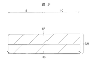
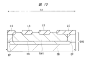
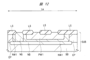
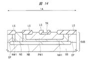
次に、本実施の形態の半導体装置の製造工程を、図面を参照して説明する。図4〜図31は、本実施の形態の半導体装置の製造工程中の要部断面図である。
<About semiconductor device manufacturing process>
Next, the manufacturing process of the semiconductor device of this embodiment will be described with reference to the drawings. 4 to 31 are fragmentary cross-sectional views of the semiconductor device of the present embodiment during the manufacturing process.
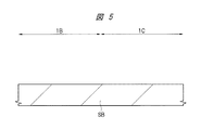
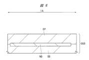
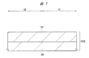
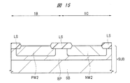
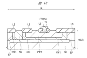
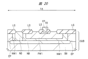
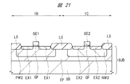
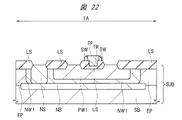
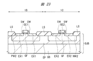
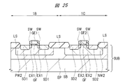
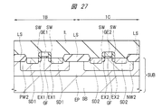
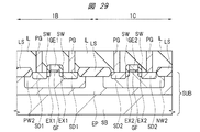
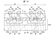
図4〜図31のうち、図4、図6、図8、図10、図12、図14、図16、図18、図20、図22、図24、図26、図28および図30には、バイポーラトランジスタ形成領域1Aの要部断面図が示されており、上記図2に相当する断面領域が示されている。また、図4〜図31のうち、図5、図7、図9、図11、図13、図15、図17、図19、図21、図23、図25、図27、図29および図31には、nMOSFET形成領域1BおよびpMOSFET形成領域1Cの要部断面図が示されている。図4〜図31には、バイポーラトランジスタ形成領域1Aにバイポーラトランジスタが、nMOSFET形成領域1Bにnチャネル型のMOSFETが、pMOSFET形成領域1Cにpチャネル型のMOSFETが、それぞれ形成される様子が示されている。
4 to 31, FIGS. 4, 6, 8, 10, 12, 14, 16, 16, 18, 20, 22, 24, 26, 28, and 30. 2 shows a cross-sectional view of the main part of the bipolar
ここで、バイポーラトランジスタ形成領域1Aは、半導体基板SUB(の主面)において、バイポーラトランジスタが形成される予定の領域である。また、nMOSFET形成領域1Bは、半導体基板SUB(の主面)において、nチャネル型MOSFETが形成される予定の領域である。また、pMOSFET形成領域1Cは、半導体基板SUB(の主面)において、pチャネル型MOSFETが形成される予定の領域である。
Here, the bipolar
なお、本願において、MOSFET(Metal Oxide Semiconductor Field Effect Transistor)というときは、ゲート絶縁膜に酸化膜(酸化シリコン膜)を用いたMISFET(Metal Insulator Semiconductor Field Effect Transistor)だけでなく、酸化膜(酸化シリコン膜)以外の絶縁膜をゲート絶縁膜に用いたMISFETも含むものとする。 In this application, MOSFET (Metal Oxide Semiconductor Field Effect Transistor) is not only a MISFET (Metal Insulator Semiconductor Field Effect Transistor) using an oxide film (silicon oxide film) as a gate insulating film, but also an oxide film (silicon oxide). It also includes a MISFET using an insulating film other than (film) as a gate insulating film.
バイポーラトランジスタ形成領域1AとnMOSFET形成領域1BとpMOSFET形成領域1Cとは、同じ半導体基板SUBに存在している。すなわち、バイポーラトランジスタ形成領域1AとnMOSFET形成領域1BとpMOSFET形成領域1Cとは、同一の半導体基板SUBの主面の互いに異なる平面領域に対応している。
The bipolar
まず、図4および図5に示されるように、基板本体SBを準備(用意)する。基板本体SBは、例えばホウ素(B)などのp型不純物が導入されたp型の単結晶シリコンなどからなる半導体基板である。 First, as shown in FIGS. 4 and 5, the substrate body SB is prepared (prepared). The substrate body SB is a semiconductor substrate made of p-type single crystal silicon into which a p-type impurity such as boron (B) is introduced.
次に、バイポーラトランジスタ形成領域1Aの基板本体SBに、n+型埋込領域NBを形成する。n+型埋込領域NBは、例えば次のようにして形成することができる。
Next, an n + type buried region NB is formed in the substrate body SB in the bipolar
すなわち、基板本体SBの表面のn+型埋込領域NB形成予定領域にアンチモン(Sb)やヒ素(As)などのn型不純物を導入し、導入したn型不純物を熱拡散させることにより、n+型埋込領域NBを形成することができる。n+型埋込領域NBは、基板本体SBの表面から所定の深さにわたって形成される。 That is, an n-type impurity such as antimony (Sb) or arsenic (As) is introduced into the n + -type buried region NB formation planned region on the surface of the substrate body SB, and the introduced n-type impurity is thermally diffused, thereby causing n A + type buried region NB can be formed. The n + type buried region NB is formed over a predetermined depth from the surface of the substrate body SB.
次に、図6および図7に示されるように、基板本体SBの主面上に、エピタキシャル層EPを形成する。これより、基板本体SBの主面上にエピタキシャル層EPが形成された半導体基板SUBが形成される。 Next, as shown in FIGS. 6 and 7, an epitaxial layer EP is formed on the main surface of the substrate body SB. Thus, the semiconductor substrate SUB in which the epitaxial layer EP is formed on the main surface of the substrate body SB is formed.
エピタキシャル層EPは、p型不純物が導入されたp−型の単結晶シリコンなどからなり、エピタキシャル成長法を用いて形成することができる。エピタキシャル層EPの不純物濃度(p型不純物濃度)は、基板本体SBの不純物濃度(p型不純物濃度)よりも低い。 The epitaxial layer EP is made of p − -type single crystal silicon into which a p-type impurity is introduced, and can be formed using an epitaxial growth method. The impurity concentration (p-type impurity concentration) of the epitaxial layer EP is lower than the impurity concentration (p-type impurity concentration) of the substrate body SB.
エピタキシャル層EPは、n+型埋込領域NB上を含む基板本体SBの主面全体上に形成される。エピタキシャル層EPをエピタキシャル成長させる際に、n+型埋込領域NB中に含まれていたn型不純物が、エピタキシャル層EP側に拡散する。このため、基板本体SBの主面上にエピタキシャル層EPを形成すると、n+型埋込領域NBの下部領域が基板本体SB内に形成され、n+型埋込領域NBの上部領域は、エピタキシャル層EP内に形成された状態になる。但し、n+型埋込領域NBは、エピタキシャル層EPの表面には達しておらず、n+型埋込領域NBの上面は、エピタキシャル層EPの表面から、所定の深さだけ深い位置にあり、n+型埋込領域NB上には、p−型のエピタキシャル層EPが存在している。 Epitaxial layer EP is formed over the entire main surface of substrate body SB including n + type buried region NB. When epitaxially growing the epitaxial layer EP, the n-type impurity contained in the n + -type buried region NB diffuses toward the epitaxial layer EP. Therefore, when an epitaxial layer EP on the main surface of the substrate main body SB, the lower region of the n + -type buried region NB is formed in the substrate main body SB, the upper region of n + -type buried region NB is epitaxial It will be in the state formed in layer EP. However, the n + type buried region NB does not reach the surface of the epitaxial layer EP, and the upper surface of the n + type buried region NB is at a position deeper than the surface of the epitaxial layer EP by a predetermined depth. A p − type epitaxial layer EP exists on the n + type buried region NB.
次に、図8および図9に示されるように、バイポーラトランジスタ形成領域1Aにおける半導体基板SUBのエピタキシャル層EPに、n型ウエルNW1を形成する。n型ウエルNW1は、例えば次のようにして形成することができる。
Next, as shown in FIGS. 8 and 9, an n-type well NW1 is formed in the epitaxial layer EP of the semiconductor substrate SUB in the bipolar
すなわち、エピタキシャル層EPのn型ウエルNW1形成予定領域に、イオン注入法などを用いてリン(P)などのn型不純物を導入し、導入したn型不純物を熱拡散させることにより、n型ウエルNW1を形成することができる。この際、n型ウエルNW1の底面(下面)がn+型埋込領域NBに達するまで熱拡散させるため、n型ウエルNW1は、n+型埋込領域NB上に、n+型埋込領域NBに接するように、形成された状態になる。このため、n型ウエルNW1の底面(下面)は、n+型埋込領域NBの上面に接している。n型ウエルNW1は、エピタキシャル層EPの表面から、n+型埋込領域NBの上面までにわたって形成される。 That is, an n-type well such as phosphorus (P) is introduced into the n-type well NW1 formation region of the epitaxial layer EP using an ion implantation method or the like, and the introduced n-type impurity is thermally diffused to thereby form an n-type well. NW1 can be formed. At this time, since the bottom surface of the n-type well NW1 (lower surface) is thermally diffused to reach the n + -type buried region NB, n-type well NW1 are on n + -type buried region NB, n + -type buried region It will be in the formed state so that it may contact NB. For this reason, the bottom surface (lower surface) of the n-type well NW1 is in contact with the upper surface of the n + -type buried region NB. The n-type well NW1 is formed from the surface of the epitaxial layer EP to the upper surface of the n + -type buried region NB.
次に、図10および図11に示されるように、半導体基板SUBに主面に、すなわちエピタキシャル層EPの主面に、絶縁膜からなる素子分離領域LSを形成する。 Next, as shown in FIGS. 10 and 11, an element isolation region LS made of an insulating film is formed on the main surface of the semiconductor substrate SUB, that is, on the main surface of the epitaxial layer EP.
ここでは、素子分離領域LSとして、LOCOS法により形成されたLOCOS酸化膜を形成した場合が示されているが、他の形態として、素子分離領域LSとして、STI法により形成したSTI絶縁膜を用いることもできる。 Here, a case where a LOCOS oxide film formed by the LOCOS method is formed as the element isolation region LS is shown, but as another embodiment, an STI insulating film formed by the STI method is used as the element isolation region LS. You can also
素子分離領域LSとして、LOCOS法を用いてLOCOS酸化膜を形成する場合は、具体的には、次のようにしてLOCOS酸化膜(素子分離領域LS)を形成することができる。 When the LOCOS oxide film is formed as the element isolation region LS using the LOCOS method, specifically, the LOCOS oxide film (element isolation region LS) can be formed as follows.
すなわち、まず、半導体基板SUBの主面(すなわちエピタキシャル層EPの主面)上に、耐熱酸化膜として用いられる窒化シリコン膜を形成してから、フォトリソグラフィ技術およびエッチング技術を用いて、LOCOS酸化膜を形成する予定の領域の窒化シリコン膜を除去する。これにより、LOCOS酸化膜を形成する予定の領域には窒化シリコン膜が形成されておらず、LOCOS酸化膜を形成しない予定の領域には窒化シリコン膜が形成されている状態が得られる。それから、熱酸化を行うことにより、窒化シリコン膜で覆われていない領域(すなわちLOCOS酸化膜を形成する予定の領域)の半導体基板SUBの表面(すなわちエピタキシャル層EPの表面)を酸化して、酸化シリコンからなるLOCOS酸化膜(素子分離領域LS)を形成する。この熱酸化の際には、窒化シリコン膜は耐熱酸化膜として機能する。このため、半導体基板SUBの表面(すなわちエピタキシャル層EPの表面)のうち、窒化シリコン膜で覆われている領域には、熱酸化膜は形成されず、従って、LOCOS酸化膜(素子分離領域LS)は形成されない。このため、LOCOS酸化膜(素子分離領域LS)は、半導体基板SUBの表面(すなわちエピタキシャル層EPの表面)のうち、窒化シリコン膜で覆われていない領域に選択的(局所的)に形成される。その後、耐熱酸化膜として用いた窒化シリコン膜を、エッチングなどにより除去し、図10および図11には、この状態が示されている。 That is, first, a silicon nitride film used as a heat-resistant oxide film is formed on the main surface of the semiconductor substrate SUB (that is, the main surface of the epitaxial layer EP), and then a LOCOS oxide film is used by using a photolithography technique and an etching technique. The silicon nitride film in the region where the film is to be formed is removed. As a result, the silicon nitride film is not formed in the region where the LOCOS oxide film is to be formed, and the silicon nitride film is formed in the region where the LOCOS oxide film is not formed. Then, by performing thermal oxidation, the surface of the semiconductor substrate SUB (that is, the surface of the epitaxial layer EP) in the region not covered with the silicon nitride film (that is, the region where the LOCOS oxide film is to be formed) is oxidized and oxidized. A LOCOS oxide film (element isolation region LS) made of silicon is formed. In this thermal oxidation, the silicon nitride film functions as a heat-resistant oxide film. For this reason, a thermal oxide film is not formed in a region covered with the silicon nitride film in the surface of the semiconductor substrate SUB (that is, the surface of the epitaxial layer EP). Therefore, the LOCOS oxide film (element isolation region LS) is not formed. Is not formed. For this reason, the LOCOS oxide film (element isolation region LS) is selectively (locally) formed in a region of the surface of the semiconductor substrate SUB (that is, the surface of the epitaxial layer EP) that is not covered with the silicon nitride film. . Thereafter, the silicon nitride film used as the heat-resistant oxide film is removed by etching or the like, and this state is shown in FIGS.
素子分離領域LSとして、STI法を用いてSTI絶縁膜を形成する場合は、具体的には、次のようにしてSTI絶縁膜(素子分離領域LS)を形成することができる。 In the case where an STI insulating film is formed using the STI method as the element isolation region LS, specifically, the STI insulating film (element isolation region LS) can be formed as follows.
すなわち、エッチングなどにより半導体基板SUBの主面(すなわちエピタキシャル層EPの主面)に素子分離溝(素子分離用の溝)を形成してから、酸化シリコン(例えばオゾンTEOS(Tetraethoxysilane)酸化膜)などからなる絶縁膜を素子分離溝を埋めるように半導体基板SUB上に形成する。それから、この絶縁膜をCMP(Chemical Mechanical Polishing:化学的機械的研磨)法などを用いて研磨することで、素子分離溝の外部の不要な絶縁膜を除去し、かつ素子分離溝内に絶縁膜を残すことにより、素子分離溝を埋める絶縁膜(絶縁体)からなるSTI絶縁膜(素子分離領域LS)を形成することができる。 That is, an element isolation groove (element isolation groove) is formed on the main surface of the semiconductor substrate SUB (that is, the main surface of the epitaxial layer EP) by etching or the like, and then silicon oxide (for example, ozone TEOS (Tetraethoxysilane) oxide film) is used. An insulating film made of is formed on the semiconductor substrate SUB so as to fill the element isolation trench. Then, the insulating film is polished using a CMP (Chemical Mechanical Polishing) method or the like to remove an unnecessary insulating film outside the element isolation groove, and the insulating film is formed in the element isolation groove. By leaving the STI, an STI insulating film (element isolation region LS) made of an insulating film (insulator) filling the element isolation trench can be formed.
次に、図12および図13に示されるように、バイポーラトランジスタ形成領域1Aにおける半導体基板SUBのエピタキシャル層EPに、n+型シンカー領域NSを形成する。n+型シンカー領域NSは、例えば次のようにして形成することができる。
Next, as shown in FIGS. 12 and 13, an n + type sinker region NS is formed in the epitaxial layer EP of the semiconductor substrate SUB in the bipolar
すなわち、エピタキシャル層EPのn+型シンカー領域NS形成予定領域に、イオン注入法などを用いてリン(P)などのn型不純物を導入し、導入したn型不純物を熱拡散させることにより、n+型シンカー領域NSを形成することができる。この際、n+型シンカー領域NSの底面(下面)がn+型埋込領域NBに達するまで熱拡散させるため、n+型シンカー領域NSは、n+型埋込領域NB上に、n+型埋込領域NBに接するように、形成された状態になる。このため、n+型シンカー領域NSは、n+型埋込領域NBの上面に接している。n+型シンカー領域NSは、エピタキシャル層EPの表面から、n+型埋込領域NBの上面までにわたって形成される。エピタキシャル層EPにおいて、n+型シンカー領域NSは、n型ウエルNW1内に形成され、n+型シンカー領域NSの不純物濃度(n型不純物濃度)は、n型ウエルNW1の不純物濃度(n型不純物濃度)よりも高い。 That is, an n-type impurity such as phosphorus (P) is introduced into the n + -type sinker region NS formation planned region of the epitaxial layer EP by using an ion implantation method or the like, and the introduced n-type impurity is thermally diffused, whereby n A + -type sinker region NS can be formed. At this time, since the bottom surface of the n + -type sinker region NS (lower surface) is thermally diffused to reach the n + -type buried region NB, n + -type sinker region NS is on the n + -type buried region NB, n + The formed state is brought into contact with the mold buried region NB. Therefore, the n + type sinker region NS is in contact with the upper surface of the n + type buried region NB. The n + type sinker region NS is formed from the surface of the epitaxial layer EP to the upper surface of the n + type buried region NB. In the epitaxial layer EP, the n + type sinker region NS is formed in the n type well NW1, and the impurity concentration (n type impurity concentration) of the n + type sinker region NS is the impurity concentration (n type impurity) of the n type well NW1. Higher than (concentration).
次に、バイポーラトランジスタ形成領域1Aにおける半導体基板SUBのエピタキシャル層EPに、p型ウエルPW1を形成する。p型ウエルPW1は、ホウ素(B)などのp型不純物をイオン注入することにより形成することができ、イオン注入の後には、熱拡散を行うことができるが、p型ウエルPW1の深さをそれほど深くする必要が無い場合は、熱拡散を省略することもできる。エピタキシャル層EPにおいて、p型ウエルPW1は、n型ウエルNW1内に、エピタキシャル層EPの表面から所定の深さにわたって形成される。
Next, a p-type well PW1 is formed in the epitaxial layer EP of the semiconductor substrate SUB in the bipolar
p型ウエルPW1の底面の深さは、n型ウエルNW1の底面の深さよりも浅いため、p型ウエルPW1の直下には、n型ウエルNW1が存在し、更にその直下には、n+型埋込領域NBが存在している。p型ウエルPW1とn+型シンカー領域NSとは、互い離間しているため、p型ウエルPW1とn+型シンカー領域NSとの間には、n型ウエルNW1が存在している。 Since the depth of the bottom surface of the p-type well PW1 is shallower than the depth of the bottom surface of the n-type well NW1, there is an n-type well NW1 immediately below the p-type well PW1, and further below that is an n + -type. An embedded region NB exists. Since the p-type well PW1 and the n + -type sinker region NS are separated from each other, the n-type well NW1 exists between the p-type well PW1 and the n + -type sinker region NS.
次に、nMOSFET形成領域1Bにおける半導体基板SUBのエピタキシャル層EPに、p型ウエルPW2を形成し、pMOSFET形成領域1Cにおける半導体基板SUBのエピタキシャル層EPに、n型ウエルNW2を形成する。
Next, the p-type well PW2 is formed in the epitaxial layer EP of the semiconductor substrate SUB in the
p型ウエルPW2は、ホウ素(B)などのp型不純物をイオン注入することにより形成することができ、n型ウエルNW2は、リン(P)などのn型不純物をイオン注入することにより形成することができる。イオン注入の後には、熱拡散を行うことができるが、p型ウエルPW2およびn型ウエルNW2の深さをそれほど深くする必要が無い場合は、熱拡散を省略することもできる。 The p-type well PW2 can be formed by ion implantation of a p-type impurity such as boron (B), and the n-type well NW2 is formed by ion implantation of an n-type impurity such as phosphorus (P). be able to. After ion implantation, thermal diffusion can be performed. However, if it is not necessary to increase the depths of the p-type well PW2 and the n-type well NW2, thermal diffusion can be omitted.
また、p型ウエルPW1とp型ウエルPW2とを、同じ不純物濃度でかつ同じ深さで形成してもよい場合は、p型ウエルPW1とp型ウエルPW2とを同工程で形成することができる。また、p型ウエルPW2とp型ウエルPW1とを別工程で形成する場合は、p型ウエルPW1を先に形成しても、あるいは、p型ウエルPW2を先に形成してもよい。 When the p-type well PW1 and the p-type well PW2 may be formed with the same impurity concentration and the same depth, the p-type well PW1 and the p-type well PW2 can be formed in the same process. . When the p-type well PW2 and the p-type well PW1 are formed in separate steps, the p-type well PW1 may be formed first or the p-type well PW2 may be formed first.
次に、図14および図15に示されるように、素子分離領域LSに溝TRを形成する。溝TRは、例えば次のようにして形成することができる。 Next, as shown in FIGS. 14 and 15, a trench TR is formed in the element isolation region LS. The trench TR can be formed as follows, for example.
すなわち、半導体基板SUBの主面上に、フォトリソグラフィ法を用いてフォトレジストパターン(図示せず)を形成する。このフォトレジストパターンは、溝TRを形成する予定の領域を露出する開口部を有している。それから、このフォトレジストパターンをエッチングマスクとして用いて、素子分離領域LSをエッチング(例えばドライエッチング)することにより、素子分離領域LSに溝TRを形成する。その後、このフォトレジストパターンは除去する。 That is, a photoresist pattern (not shown) is formed on the main surface of the semiconductor substrate SUB using a photolithography method. The photoresist pattern has an opening that exposes a region where the trench TR is to be formed. Then, using this photoresist pattern as an etching mask, the element isolation region LS is etched (for example, dry etching), thereby forming a trench TR in the element isolation region LS. Thereafter, the photoresist pattern is removed.
溝TRは、バイポーラトランジスタ形成領域1Aの素子分離領域LSに形成されるが、素子分離領域LSを貫通してはおらず、溝TRの底面(下面)は素子分離領域LSの厚みの途中に位置している。このため、溝TRの直下には、素子分離領域LSが存在しているが、溝TRの直下の素子分離領域LSの厚みは、溝TRが形成されていない領域における素子分離領域LSの厚みよりも、溝TRの深さの分だけ、小さく(薄く)なっている。
The trench TR is formed in the element isolation region LS of the bipolar
次に、図16および図17に示されるように、半導体基板SUBのエピタキシャル層EPの表面に、ゲート絶縁膜用の絶縁膜GFを形成する。絶縁膜GFは、薄い酸化シリコン膜などからなり、熱酸化法などを用いて形成することができる。 Next, as shown in FIGS. 16 and 17, an insulating film GF for a gate insulating film is formed on the surface of the epitaxial layer EP of the semiconductor substrate SUB. The insulating film GF is made of a thin silicon oxide film or the like and can be formed using a thermal oxidation method or the like.
絶縁膜GFは、素子分離領域LSが形成されていない領域のエピタキシャル層EPの表面に形成される。このため、nMOSFET形成領域1BおよびpMOSFET形成領域1Cだけでなく、バイポーラトランジスタ形成領域1Aにおいても、エピタキシャル層EPの表面に絶縁膜GFが形成される。但し、nMOSFET形成領域1BおよびpMOSFET形成領域1Cの絶縁膜GFは、ゲート絶縁膜用に形成したものであるが、バイポーラトランジスタ形成領域1Aの絶縁膜GFは、ゲート絶縁膜としては用いられない。
The insulating film GF is formed on the surface of the epitaxial layer EP in a region where the element isolation region LS is not formed. Therefore, the insulating film GF is formed on the surface of the epitaxial layer EP not only in the
次に、半導体基板SUBの主面(すなわちエピタキシャル層EPの主面)全面上に、すなわち、絶縁膜GFおよび素子分離領域LS上に、導電膜としてシリコン膜PSを形成(堆積)する。この際、溝TR内は、シリコン膜PSにより埋め込まれる。 Next, a silicon film PS is formed (deposited) as a conductive film over the entire main surface of the semiconductor substrate SUB (ie, the main surface of the epitaxial layer EP), that is, over the insulating film GF and the element isolation region LS. At this time, the trench TR is filled with the silicon film PS.
シリコン膜PSは、多結晶シリコン膜(ポリシリコン膜)からなり、CVD(Chemical Vapor Deposition:化学的気相成長)法などを用いて形成することができる。成膜時はシリコン膜PSをアモルファスシリコン膜として形成してから、その後の熱処理で、アモルファスシリコン膜からなるシリコン膜PSを、多結晶シリコン膜からなるシリコン膜PSに変えることもできる。また、シリコン膜PSの成膜後に、シリコン膜PSに不純物をイオン注入することなどにより、シリコン膜PSを低抵抗の半導体膜(ドープトポリシリコン膜)とすることができる。この際、nMOSFET形成領域1Bのシリコン膜PSとバイポーラトランジスタ形成領域1Aのシリコン膜PSとには、リン(P)などのn型不純物を導入し、pMOSFET形成領域1Cのシリコン膜PSには、ホウ素(B)などのp型不純物を導入することが好ましい。シリコン膜PSは、ゲート電極GE1,GE2形成用の導電膜と、電極FP形成用の導電膜とを兼ねている。
The silicon film PS is made of a polycrystalline silicon film (polysilicon film) and can be formed using a CVD (Chemical Vapor Deposition) method or the like. At the time of film formation, after the silicon film PS is formed as an amorphous silicon film, the silicon film PS made of an amorphous silicon film can be changed to a silicon film PS made of a polycrystalline silicon film by subsequent heat treatment. In addition, after the silicon film PS is formed, impurities can be ion-implanted into the silicon film PS, thereby making the silicon film PS a low-resistance semiconductor film (doped polysilicon film). At this time, an n-type impurity such as phosphorus (P) is introduced into the silicon film PS in the
次に、図18および図19に示されるように、フォトリソグラフィ法およびエッチング法を用いてシリコン膜PSをパターニングすることにより、電極FPとゲート電極GE1とゲート電極GE2とを形成する。 Next, as shown in FIGS. 18 and 19, the silicon film PS is patterned by using a photolithography method and an etching method, thereby forming the electrode FP, the gate electrode GE1, and the gate electrode GE2.
電極FPとゲート電極GE1とゲート電極GE2とは、それぞれパターニングされたシリコン膜PSからなり、共通のシリコン膜PSを用いて同工程で形成することができる。ゲート電極GE1は、nMOSFET形成領域1Bにおいて、p型ウエルPW2上に絶縁膜GFを介して形成され、ゲート電極GE2は、pMOSFET形成領域1Cにおいて、n型ウエルNW2上に絶縁膜GFを介して形成される。電極FPは、バイポーラトランジスタ形成領域1Aにおいて、素子分離領域LS上に、溝TR内を埋めるように形成される。
The electrode FP, the gate electrode GE1, and the gate electrode GE2 are each formed of a patterned silicon film PS, and can be formed in the same process using a common silicon film PS. The gate electrode GE1 is formed on the p-type well PW2 via the insulating film GF in the
また、電極FPとゲート電極GE1,GE2とは、共通の導電膜(ここではシリコン膜PS)を用いて同工程で形成することができるため、半導体装置の製造工程数を抑制することができる。 In addition, since the electrode FP and the gate electrodes GE1 and GE2 can be formed in the same step using a common conductive film (here, the silicon film PS), the number of manufacturing steps of the semiconductor device can be suppressed.
ゲート電極GE1がnチャネル型MIFFETのゲート電極となり、そのゲート電極GE1の下に残存する絶縁膜GFが、nチャネル型MOSFETのゲート絶縁膜となる。また、ゲート電極GE2がpチャネル型MIFFETのゲート電極となり、そのゲート電極GE2の下に残存する絶縁膜GFが、pチャネル型MOSFETのゲート絶縁膜となる。ゲート電極GE1,GE2で覆われない部分の絶縁膜GFは、シリコン膜PSをパターニングする際のドライエッチングや、あるいはそのドライエッチング後にウェットエッチングを行うことによって除去され得る。 The gate electrode GE1 becomes the gate electrode of the n-channel type MIFFET, and the insulating film GF remaining under the gate electrode GE1 becomes the gate insulating film of the n-channel type MOSFET. Further, the gate electrode GE2 becomes the gate electrode of the p-channel type MIFFET, and the insulating film GF remaining under the gate electrode GE2 becomes the gate insulating film of the p-channel type MOSFET. The portion of the insulating film GF that is not covered with the gate electrodes GE1 and GE2 can be removed by dry etching when patterning the silicon film PS or by performing wet etching after the dry etching.
次に、図20および図21に示されるように、ゲート電極GE1をマスクとして用いてnMOSFET形成領域1Bのp型ウエルPW2にヒ素(As)などのn型不純物をイオン注入することにより、p型ウエルPW2において、ゲート電極GE1の両側にn−型半導体領域EX1を形成する。また、ゲート電極GE2をマスクとして用いてpMOSFET形成領域1Cのn型ウエルNW2にホウ素(B)などのp型不純物をイオン注入することにより、n型ウエルNW2において、ゲート電極GE2の両側にp−型半導体領域EX2を形成する。n−型半導体領域EX1を形成するイオン注入とp−型半導体領域EX2を形成するイオン注入とは、どちらを先に行ってもよい。
Next, as shown in FIGS. 20 and 21, an n-type impurity such as arsenic (As) is ion-implanted into the p-type well PW2 of the
次に、図22および図23に示されるように、半導体基板SUBの主面上に、電極FPおよびゲート電極GE1,GE2を覆うように、サイドウォールスペーサ形成用の絶縁膜を形成してから、その絶縁膜を異方性エッチングすることにより、ゲート電極GE1,GE2の側壁上にサイドウォールスペーサ(側壁絶縁膜)SWを形成する。この際、ゲート電極GE1,GE2の側壁上だけでなく、電極FPの側壁上にもサイドウォールスペーサSWが形成され得る。 Next, as shown in FIGS. 22 and 23, after forming an insulating film for forming a sidewall spacer on the main surface of the semiconductor substrate SUB so as to cover the electrode FP and the gate electrodes GE1 and GE2, The insulating film is anisotropically etched to form side wall spacers (side wall insulating films) SW on the side walls of the gate electrodes GE1 and GE2. At this time, the sidewall spacer SW can be formed not only on the sidewalls of the gate electrodes GE1 and GE2, but also on the sidewalls of the electrode FP.
次に、図24および図25に示されるように、ゲート電極GE1とその側壁上のサイドウォールスペーサSWをマスクとして用いてnMOSFET形成領域1Bのp型ウエルPW2にヒ素(As)などのn型不純物をイオン注入することにより、p型ウエルPW2において、ゲート電極GE1とその側壁上のサイドウォールスペーサSWからなる構造体の両側に、n+型半導体領域SD1を形成する。また、ゲート電極GE2とその側壁上のサイドウォールスペーサSWをマスクとして用いてpMOSFET形成領域1Cのn型ウエルNW2にホウ素(B)などのp型不純物をイオン注入することにより、n型ウエルNW2において、ゲート電極GE2およびその側壁上のサイドウォールスペーサSWからなる構造体の両側に、p+型半導体領域SD2を形成する。
Next, as shown in FIGS. 24 and 25, an n-type impurity such as arsenic (As) is formed in the p-type well PW2 of the
n+型半導体領域SD1は、n−型半導体領域EX1よりも接合深さが深くかつ不純物濃度(n型不純物濃度)が高く、また、p+型半導体領域SD2は、p−型半導体領域EX2よりも接合深さが深くかつ不純物濃度(p型不純物濃度)が高い。nMOSFET形成領域1Bにおいて、n−型半導体領域EX1およびn+型半導体領域SD1により、nチャネル型MOSFETのLDD(lightly doped drain)構造を有するソース・ドレイン領域が形成される。また、pMOSFET形成領域1Cにおいて、p−型半導体領域EX2およびp+型半導体領域SD2により、pチャネル型MOSFETのLDD構造を有するソース・ドレイン領域が形成される。
The n + type semiconductor region SD1 has a deeper junction depth and a higher impurity concentration (n type impurity concentration) than the n − type semiconductor region EX1, and the p + type semiconductor region SD2 is higher than the p − type semiconductor region EX2. Also, the junction depth is deep and the impurity concentration (p-type impurity concentration) is high. In the
また、n+型半導体領域SD1を形成するイオン注入の際には、nMOSFET形成領域1Bにn+型半導体領域SD1が形成されるだけでなく、バイポーラトランジスタ形成領域1Aのエピタキシャル層EPにn型不純物がイオン注入されることにより、n+型半導体領域NR1およびn+型半導体領域NR2が形成される。また、p+型半導体領域SD2を形成するイオン注入の際には、pMOSFET形成領域1Cにp+型半導体領域SD2が形成されるだけでなく、バイポーラトランジスタ形成領域1Aのエピタキシャル層EPにp型不純物がイオン注入されることにより、p+型半導体領域PR1が形成される。
Further, during the ion implantation for forming the n + -type semiconductor regions SD1, not only the n + -type semiconductor region SD1 is formed on the
つまり、バイポーラトランジスタ形成領域1Aのn+型半導体領域NR1およびn+型半導体領域NR2は、nMOSFET形成領域1Bのn+型半導体領域SD1と、共通のイオン注入工程により形成され、また、バイポーラトランジスタ形成領域1Aのp+型半導体領域PR1は、pMOSFET形成領域1Cのp+型半導体領域SD2と、共通のイオン注入工程により形成される。
That is, the n + -type semiconductor region NR1 and the n + -type semiconductor region NR2 in the bipolar
n+型半導体領域SD1、n+型半導体領域NR1およびn+型半導体領域NR2を形成するイオン注入の際には、pMOSFET形成領域1C全体と、バイポーラトランジスタ形成領域1Aにおけるp+型半導体領域PR1を形成すべき領域とを、フォトレジストパターンで覆っておけばよい。また、p+型半導体領域SD2およびp+型半導体領域PR1を形成するイオン注入の際には、nMOSFET形成領域1B全体と、バイポーラトランジスタ形成領域1Aにおけるn+型半導体領域NR1,NR2を形成すべき領域とを、フォトレジストパターンで覆っておけばよい。また、n+型半導体領域SD1、n+型半導体領域NR1およびn+型半導体領域NR2を形成するイオン注入と、p+型半導体領域SD2およびp+型半導体領域PR1を形成するイオン注入とは、どちらを先に行ってもよい。
During ion implantation for forming the n + type semiconductor region SD1, the n + type semiconductor region NR1, and the n + type semiconductor region NR2, the entire
次に、これまでに導入した不純物を活性化させるための熱処理である活性化アニールを行う。 Next, activation annealing, which is a heat treatment for activating the impurities introduced so far, is performed.
次に、必要に応じて、n+型半導体領域SD1、p+型半導体領域SD2、n+型半導体領域NR1、n+型半導体領域NR2、p+型半導体領域PR1、ゲート電極GE1およびゲート電極GE2の各表面(表層部分)に、サリサイド(Salicide:Self Aligned Silicide)技術などにより、それぞれ金属シリサイド層(図示せず)を形成する。金属シリサイド層を形成すれば、コンタクト抵抗などを低減できるが、金属シリサイド層の形成は省略することもできる。 Next, as required, the n + type semiconductor region SD1, the p + type semiconductor region SD2, the n + type semiconductor region NR1, the n + type semiconductor region NR2, the p + type semiconductor region PR1, the gate electrode GE1, and the gate electrode GE2 A metal silicide layer (not shown) is formed on each surface (surface layer portion) by using a salicide (Self Aligned Silicide) technique. If a metal silicide layer is formed, the contact resistance can be reduced, but the formation of the metal silicide layer can be omitted.
次に、図26および図27に示されるように、半導体基板SUBの主面上に、すなわちエピタキシャル層EP上に、素子分離領域LS、電極FP、ゲート電極GE1,GE2およびサイドウォールスペーサSWを覆うように、絶縁膜として層間絶縁膜ILを形成する。層間絶縁膜ILは、例えば酸化シリコン膜などからなり、CVD法などを用いて形成することができる。層間絶縁膜ILとして、積層絶縁膜を用いることも可能である。層間絶縁膜ILの成膜後、CMP法により層間絶縁膜ILの上面を研磨するなどして、層間絶縁膜ILの上面の平坦性を高めることもできる。 Next, as shown in FIGS. 26 and 27, the element isolation region LS, the electrode FP, the gate electrodes GE1 and GE2, and the sidewall spacer SW are covered on the main surface of the semiconductor substrate SUB, that is, on the epitaxial layer EP. As described above, the interlayer insulating film IL is formed as the insulating film. The interlayer insulating film IL is made of, for example, a silicon oxide film or the like, and can be formed using a CVD method or the like. A laminated insulating film can also be used as the interlayer insulating film IL. After the formation of the interlayer insulating film IL, the flatness of the upper surface of the interlayer insulating film IL can be improved by polishing the upper surface of the interlayer insulating film IL by a CMP method.
次に、図28および図29に示されるように、層間絶縁膜ILにコンタクトホールを形成する。コンタクトホールは、例えば、フォトリソグラフィ法を用いて層間絶縁膜IL上に形成したフォトレジストパターン(図示せず)をエッチングマスクとして、層間絶縁膜ILをドライエッチングすることにより、形成することができる。コンタクトホールは、層間絶縁膜ILを貫通している。 Next, as shown in FIGS. 28 and 29, contact holes are formed in the interlayer insulating film IL. The contact hole can be formed, for example, by dry etching the interlayer insulating film IL using a photoresist pattern (not shown) formed on the interlayer insulating film IL by photolithography as an etching mask. The contact hole penetrates the interlayer insulating film IL.
次に、層間絶縁膜ILのコンタクトホール内に、接続用の導電体部として、タングステン(W)などからなる導電性のプラグPGを形成する。 Next, a conductive plug PG made of tungsten (W) or the like is formed as a connecting conductor portion in the contact hole of the interlayer insulating film IL.
プラグPGを形成するには、例えば、コンタクトホールの内部(底部および側壁上)を含む層間絶縁膜IL上に、バリア導体膜を形成する。このバリア導体膜は、例えば、チタン膜、窒化チタン膜、あるいはそれらの積層膜からなる。それから、このバリア導体膜上にタングステン膜などからなる主導体膜を、コンタクトホールを埋めるように形成する。それから、コンタクトホールの外部の不要な主導体膜およびバリア導体膜をCMP法またはエッチバック法などによって除去することにより、コンタクトホール内に埋め込まれて残存する主導体膜およびバリア導体膜からなるプラグPGを形成することができる。なお、図面の簡略化のために、図28および図29では、プラグPGを構成するバリア導体膜および主導体膜を一体化して示してある。 In order to form the plug PG, for example, a barrier conductor film is formed on the interlayer insulating film IL including the inside (on the bottom and side walls) of the contact hole. This barrier conductor film is made of, for example, a titanium film, a titanium nitride film, or a laminated film thereof. Then, a main conductor film made of a tungsten film or the like is formed on the barrier conductor film so as to fill the contact hole. Then, unnecessary main conductor film and barrier conductor film outside the contact hole are removed by CMP method or etch back method, etc., so that the plug PG composed of the main conductor film and barrier conductor film remaining embedded in the contact hole is obtained. Can be formed. For simplification of the drawings, in FIGS. 28 and 29, the barrier conductor film and the main conductor film constituting the plug PG are shown in an integrated manner.
バイポーラトランジスタ形成領域1Aにおいては、プラグPGとして、エミッタ用プラグPGE、ベース用プラグPGB、コレクタ用プラグPGCおよびプラグPGFが形成される。エミッタ用プラグPGEは、n+型半導体領域NR1上に形成されてn+型半導体領域NR1と電気的に接続され、ベース用プラグPGBは、p+型半導体領域PR1上に形成されてp+型半導体領域PR1と電気的に接続される。また、コレクタ用プラグPGCは、n+型半導体領域NR2上に形成されてn+型半導体領域NR2と電気的に接続され、プラグPGFは、電極FP上に形成されて電極FPと電気的に接続される。nMOSFET形成領域1Bにおいては、n+型半導体領域SD1上とゲート電極GE1上とにそれぞれプラグPGが形成され、pMOSFET形成領域1Cにおいては、p+型半導体領域SD2上とゲート電極GE2上とにそれぞれプラグPGが形成される。
In the bipolar
次に、図30および図31に示されるように、プラグPGが埋め込まれた層間絶縁膜IL上に、第1層目の配線である配線M1を形成する。 Next, as shown in FIGS. 30 and 31, a wiring M <b> 1 that is a first-layer wiring is formed on the interlayer insulating film IL in which the plug PG is embedded.
配線M1は、例えば、次のようにして形成することができる。すなわち、まず、プラグPGが埋め込まれた層間絶縁膜IL上に、バリア導体膜とその上の主導体膜とその上のバリア導体膜とからなる積層導電膜を形成する。バリア導体膜は、例えば、チタン膜、窒化チタン膜、あるいはそれらの積層膜からなり、主導体膜は、例えば、アルミニウムを主体とする導体膜(アルミニウム膜またはアルミニウム合金膜)からなる。それから、その積層導電膜をフォトリソグラフィ法およびドライエッチング法を用いてパターニングすることにより、パターニングされた積層導電膜からなる配線M1を形成することができる。図30および図31では、図面の簡略化のために、配線M1は、バリア導体膜および主導体膜を一体化して示してある。 The wiring M1 can be formed as follows, for example. That is, first, a laminated conductive film comprising a barrier conductor film, a main conductor film thereon, and a barrier conductor film thereon is formed on the interlayer insulating film IL in which the plug PG is embedded. The barrier conductor film is made of, for example, a titanium film, a titanium nitride film, or a laminated film thereof, and the main conductor film is made of, for example, a conductor film (aluminum film or aluminum alloy film) mainly composed of aluminum. Then, the wiring M1 made of the patterned laminated conductive film can be formed by patterning the laminated conductive film by using a photolithography method and a dry etching method. 30 and 31, for the sake of simplification, the wiring M1 shows the barrier conductor film and the main conductor film in an integrated manner.
バイポーラトランジスタ形成領域1Aにおいては、配線M1として、エミッタ用配線M1E、ベース用配線M1Bおよびコレクタ用配線M1Cが形成される。エミッタ用配線M1Eは、エミッタ用プラグPGEを介してn+型半導体領域NR1に電気的に接続されるとともに、プラグPGFを介して電極FPに電気的に接続される。また、ベース用配線M1Bは、ベース用プラグPGBを介してp+型半導体領域PR1に電気的に接続され、コレクタ用配線M1Cは、コレクタ用プラグPGCを介してn+型半導体領域NR2に電気的に接続される。また、nMOSFET形成領域1BおよびpMOSFET形成領域1Cにも配線M1が形成され、その配線M1は、プラグPGを介して、n+型半導体領域SD1、p+型半導体領域SD2、ゲート電極GE1あるいはゲート電極GE2などと電気的に接続される。
In the bipolar
また、ここでは、導電膜をパターニングすることにより配線M1を形成する場合について説明したが、他の形態として、配線M1として、ダマシン法で形成したダマシン配線(埋込配線)を用いることも可能である。 Although the case where the wiring M1 is formed by patterning the conductive film has been described here, a damascene wiring (embedded wiring) formed by a damascene method can be used as the wiring M1 as another embodiment. is there.
その後、更に上層の層間絶縁膜および配線が形成されるが、ここではその図示および説明は省略する。 Thereafter, an upper interlayer insulating film and wiring are formed, but illustration and description thereof are omitted here.
<検討例について>
本発明者が検討した検討例の半導体装置について説明する。図32は、本発明者が検討した第1検討例の半導体装置の要部断面図であり、図33は、本発明者が検討した第2検討例の半導体装置の要部断面図であり、いずれも本実施の形態の上記図1に相当する断面が示されている。
<About study example>
A semiconductor device of a study example studied by the present inventors will be described. FIG. 32 is a cross-sectional view of a main part of the semiconductor device of the first study example studied by the present inventor, and FIG. 33 is a cross-sectional view of the main part of the semiconductor device of the second study example studied by the present inventor. Each shows a cross section corresponding to FIG. 1 of the present embodiment.
図32に示される第1検討例の半導体装置および図33に示される第2検討例の半導体装置は、いずれもバイポーラトランジスタを有する半導体装置である。 The semiconductor device of the first study example shown in FIG. 32 and the semiconductor device of the second study example shown in FIG. 33 are both semiconductor devices having bipolar transistors.
図32に示される第1検討例の半導体装置は、上記電極FPに相当するものが形成されておらず、従って、上記溝TRに相当するものや上記プラグPGFに相当するものも形成されていない。従って、図32に示される第1検討例の半導体装置では、層間絶縁膜IL上には上記エミッタ用配線M1Eの代わりにエミッタ用配線M1E100が形成されている。 The semiconductor device of the first study example shown in FIG. 32 is not formed with the one corresponding to the electrode FP, and therefore the one corresponding to the trench TR or the one corresponding to the plug PGF is not formed. . Therefore, in the semiconductor device of the first study example shown in FIG. 32, the emitter wiring M1E100 is formed on the interlayer insulating film IL instead of the emitter wiring M1E.
それ以外の構成は、図32に示される第1検討例の半導体装置も上記図1〜図3の半導体装置とほぼ同様であるので、ここではその繰り返しの説明は省略する。 Since the other configuration of the semiconductor device of the first study example shown in FIG. 32 is substantially the same as that of the semiconductor device of FIGS. 1 to 3, repeated description thereof is omitted here.
バイポーラトランジスタの構成は、図32に示される第1検討例の半導体装置も、上記図1〜図3の半導体装置とほぼ同様である。すなわち、上記図1〜図3の半導体装置と同様に、図32に示される第1検討例の半導体装置においても、n+型半導体領域NR1が、バイポーラトランジスタのエミッタ領域として機能し、p型ウエルPW1およびp+型半導体領域PR1が、バイポーラトランジスタのベース領域として機能する。また、n型ウエルNW1、n+型埋込領域NB、n+型シンカー領域NSおよびn+型半導体領域NR2が、バイポーラトランジスタのコレクタ領域として機能する。つまり、エミッタ領域を取り囲むようにベース領域が配置され、ベース領域を取り囲むようにコレクタ領域が配置されている。エミッタ用プラグPGEからエミッタ用のn+型半導体領域NR1にエミッタ電圧が供給され、ベース用プラグPGBからベース用のp+型半導体領域PR1にベース電圧が供給され、コレクタ用プラグPGCからコレクタ用のn+型半導体領域NR2にコレクタ電圧が供給される。 The structure of the bipolar transistor is substantially the same as that of the semiconductor device of the first study example shown in FIG. That is, in the semiconductor device of the first study example shown in FIG. 32 as well as the semiconductor devices of FIGS. 1 to 3, the n + type semiconductor region NR1 functions as the emitter region of the bipolar transistor, PW1 and p + type semiconductor region PR1 function as the base region of the bipolar transistor. Further, the n-type well NW1, the n + -type buried region NB, the n + -type sinker region NS, and the n + -type semiconductor region NR2 function as a collector region of the bipolar transistor. That is, the base region is disposed so as to surround the emitter region, and the collector region is disposed so as to surround the base region. The emitter voltage is supplied from the emitter plug PGE to the emitter n + type semiconductor region NR1, the base voltage is supplied from the base plug PGB to the base p + type semiconductor region PR1, and the collector plug PGC supplies the collector voltage to the collector. A collector voltage is supplied to the n + type semiconductor region NR2.
図1〜図3の半導体装置と同様に、図32に示される第1検討例の半導体装置においても、エミッタ用のn+型半導体領域NR1とベース用のp+型半導体領域PR1との間の半導体基板SUBの主面には、素子分離領域LSが形成されている。 Similar to the semiconductor device of FIGS. 1 to 3, also in the semiconductor device of the first study example shown in FIG. 32, between the n + type semiconductor region NR1 for emitter and the p + type semiconductor region PR1 for base. An element isolation region LS is formed on the main surface of the semiconductor substrate SUB.
バイポーラトランジスタにおいては、エミッタ・ベース間に逆方向バイアスを印加すると、hFE特性(電流増幅率:ベース電流に対するコレクタ電流の比率)が劣化し、バイポーラトランジスタの特性が劣化してしまうという問題がある。 In the bipolar transistor, when a reverse bias is applied between the emitter and the base, the hFE characteristic (current amplification factor: the ratio of the collector current to the base current) is deteriorated, and the characteristic of the bipolar transistor is deteriorated.
具体的に説明すると、エミッタ・ベース間に逆方向バイアスを印加すると、エミッタからベース側に伸びた空乏層による電界集中によりホットキャリア(ここではホール)が発生してしまう。本発明者のシミュレーションによれば、エミッタ・ベース間に逆方向バイアスを印加すると、図32において、符号RGを付して示した領域で電界集中が生じてホットキャリアが発生しやすい。発生したホットキャリアは、近くにある素子分離領域LSにトラップ(捕獲)されてしまい、逆方向バイアスの印加を止めても、素子分離領域LS中にトラップされたまま残ってしまう虞がある。これは、バイポーラトランジスタの通常動作時(通常動作時はエミッタ・ベース間に順方向バイアスが印加される)に、悪影響を与えてしまう。例えば、エミッタからの電子がコレクタ側に移動する途中で、素子分離領域LS中にトラップされていたホールと再結合してしまい、これがベース電流の増加につながるため、hFE特性(電流増幅率)を劣化させ、バイポーラトランジスタの特性を劣化させてしまう。また、エミッタ・ベース間に逆方向バイアスを印加したときに、電界集中によって発生したホットキャリアが、近くにある素子分離領域LSと半導体基板SUB(エピタキシャル層EP)との界面に衝突してダメージを与えてしまう虞もあり、これも、バイポーラトランジスタの通常動作時に、悪影響を与えてしまう。 More specifically, when a reverse bias is applied between the emitter and the base, hot carriers (here, holes) are generated due to electric field concentration by a depletion layer extending from the emitter to the base side. According to the simulation of the present inventor, when a reverse bias is applied between the emitter and the base, electric field concentration occurs in a region indicated by reference numeral RG in FIG. 32 and hot carriers are likely to be generated. The generated hot carriers are trapped (captured) in a nearby element isolation region LS, and may remain trapped in the element isolation region LS even when the reverse bias is stopped. This adversely affects the normal operation of the bipolar transistor (a forward bias is applied between the emitter and the base during normal operation). For example, while electrons from the emitter move to the collector side, they recombine with holes trapped in the element isolation region LS, which leads to an increase in base current. It degrades and degrades the characteristics of the bipolar transistor. In addition, when a reverse bias is applied between the emitter and the base, hot carriers generated by electric field concentration collide with the interface between the element isolation region LS and the semiconductor substrate SUB (epitaxial layer EP) nearby, and damage is caused. This also has an adverse effect on the normal operation of the bipolar transistor.
近年、例えば車載用途などでは、高い信頼性が求められるようになってきており、逆方向バイアスが印加されても、バイポーラトランジスタの特性が劣化しないような、高い信頼性を有する半導体装置が求められている。 In recent years, for example, in-vehicle applications, high reliability has been demanded, and there is a need for a highly reliable semiconductor device that does not deteriorate the characteristics of a bipolar transistor even when a reverse bias is applied. ing.
バイポーラトランジスタの正常動作時には、エミッタ・ベース間に順方向バイアスが印加されるが、信頼性向上のためには、エミッタ・ベース間に逆方向バイアスが印加されても、バイポーラトランジスタの正常動作時の特性が劣化(変動)しないことが求められる。 During normal operation of the bipolar transistor, a forward bias is applied between the emitter and the base. However, in order to improve reliability, even if a reverse bias is applied between the emitter and base, It is required that the characteristics do not deteriorate (fluctuate).
そこで、本発明者は、図33に示される第2検討例の半導体装置について検討した。 Therefore, the present inventor studied the semiconductor device of the second study example shown in FIG.
図33に示される第2検討例の半導体装置は、エミッタ用のn+型半導体領域NR1とベース用のp+型半導体領域PR1との間の素子分離領域LS上に、フィールドプレート電極として電極FP200が形成されている。この電極FP200は、プラグPGF200を介して、エミッタ用配線M1E200に電気的に接続されている。 The semiconductor device of the second study example shown in FIG. 33 has an electrode FP200 as a field plate electrode on the element isolation region LS between the n + type semiconductor region NR1 for emitter and the p + type semiconductor region PR1 for base. Is formed. The electrode FP200 is electrically connected to the emitter wiring M1E200 via the plug PGF200.
エミッタ用配線M1E200は、上記エミッタ用配線M1Eに相当するものであり、エミッタ用プラグPGEを介してエミッタ用のn+型半導体領域NR1に電気的に接続されるとともに、プラグPGF200を介して、電極FP200に電気的に接続されている。つまり、電極FP200と、エミッタ用のn+型半導体領域NR1とは、プラグPGF200、エミッタ用配線M1E200およびエミッタ用プラグPGEを介して、電気的に接続されている。このため、電極FP200と、エミッタ用のn+型半導体領域NR1とに、同じ電圧(エミッタ電圧)が供給され、両者は実質的に同電位になる。 The emitter wiring M1E200 corresponds to the emitter wiring M1E, and is electrically connected to the emitter n + -type semiconductor region NR1 through the emitter plug PGE and is connected to the electrode through the plug PGF200. It is electrically connected to the FP 200. That is, the electrode FP200 and the emitter n + type semiconductor region NR1 are electrically connected via the plug PGF200, the emitter wiring M1E200, and the emitter plug PGE. For this reason, the same voltage (emitter voltage) is supplied to the electrode FP200 and the n + -type semiconductor region NR1 for emitter, and both have substantially the same potential.
図33に示される第2検討例における電極FP200が上記電極FPと相違しているのは、次の点である。すなわち、上記電極FPは、素子分離領域LSに形成された上記溝TR内に埋め込まれているのに対して、図33に示される第2検討例の半導体装置では、素子分離領域LSに上記溝TRに相当するものは形成されておらず、従って、電極FP200は、素子分離領域LSの溝に埋め込まれているのではなく、溝が形成されていない素子分離領域LS上に配置されている。 The electrode FP200 in the second study example shown in FIG. 33 is different from the electrode FP in the following points. That is, the electrode FP is embedded in the trench TR formed in the element isolation region LS, whereas in the semiconductor device of the second study example shown in FIG. 33, the groove is formed in the element isolation region LS. No equivalent of TR is formed, and therefore the electrode FP200 is not embedded in the trench of the element isolation region LS, but is disposed on the element isolation region LS where no trench is formed.
図33に示される第2検討例の場合は、エミッタ用のn+型半導体領域NR1に供給される電圧と同じ電圧が、電極FP200に供給される。このため、エミッタ・ベース間に逆方向バイアスを印加した場合、図32に示される第1検討例よりも、図33に示される第2検討例の方が、エミッタからベース側への空乏層の伸びを促進できるため、電界集中を緩和することができる。すなわち、エミッタ・ベース間に逆方向バイアスを印加した場合、図32に示される第1検討例では、符号RGで示した領域で電界集中が生じてホットキャリアが発生しやすいが、それに比べると、図33に示される第2検討例では、その領域RGで電界集中が生じにくくなり、ホットキャリアの発生を抑制することができる。 In the case of the second study example shown in FIG. 33, the same voltage as that supplied to the emitter n + -type semiconductor region NR1 is supplied to the electrode FP200. Therefore, when a reverse bias is applied between the emitter and the base, the depletion layer from the emitter to the base side is better in the second study example shown in FIG. 33 than in the first study example shown in FIG. Since elongation can be promoted, electric field concentration can be relaxed. That is, when a reverse bias is applied between the emitter and base, in the first study example shown in FIG. 32, electric field concentration is likely to occur in the region indicated by reference numeral RG, and hot carriers are likely to be generated. In the second study example shown in FIG. 33, electric field concentration is less likely to occur in the region RG, and generation of hot carriers can be suppressed.
このため、図32に示される第1検討例よりも、図33に示される第2検討例の方が、電極FP200を設けたことにより、エミッタ・ベース間に逆方向バイアスを印加したときの電界集中を緩和することができ、ホットキャリアの発生を抑制することができるため、そのホットキャリアの発生に伴う上述した問題が生じにくくなる。 For this reason, in the second study example shown in FIG. 33, the electrode FP200 is provided in the second study example shown in FIG. 32, so that an electric field when a reverse bias is applied between the emitter and the base is provided. Since concentration can be relaxed and generation of hot carriers can be suppressed, the above-described problems associated with the generation of hot carriers are less likely to occur.
電極FP200は、エミッタ用のn+型半導体領域NR1とベース用のp+型半導体領域PR1との間の素子分離領域LS上に配置する必要がある。しかしながら、素子分離領域LSの厚みが厚いと、電極FP200と基板領域(ここではp型ウエルPW1)との間の距離が大きくなるため、電極FP200を設けたことによる、エミッタ・ベース間に逆方向バイアスを印加したときの電界集中を緩和してホットキャリアの発生を抑制する効果が薄れてしまう。かといって、素子分離領域LS全体の厚みを薄くしてしまうと、エミッタ用のn+型半導体領域NR1とベース用のp+型半導体領域PR1との間に素子分離領域LSを設けてエミッタ・ベース間の耐圧を向上させる効果が薄れてしまう。つまり、エミッタ用のn+型半導体領域NR1とベース用のp+型半導体領域PR1との間の素子分離領域LS上に電極FP200を形成した第2検討例の場合、電極FP200による電界集中緩和効果を高めるためには、素子分離領域LSの厚みを薄くすることが有利であるが、エミッタ・ベース間の耐圧を向上させるためには、素子分離領域LSの厚みを厚くする方が有利である。このため、図33に示される第2検討例の構造では、電極FP200による電界集中緩和効果をできるだけ向上させることと、エミッタ・ベース間の耐圧をできるだけ向上させることとは、両立させ難い。すなわち、図33に示される第2検討例の構造では、電極FP200による電界集中緩和効果を十分に発揮させることは難しい。 The electrode FP200 needs to be disposed on the element isolation region LS between the n + type semiconductor region NR1 for emitter and the p + type semiconductor region PR1 for base. However, if the element isolation region LS is thick, the distance between the electrode FP200 and the substrate region (here, the p-type well PW1) increases, and therefore the reverse direction between the emitter and the base due to the provision of the electrode FP200. The effect of suppressing the generation of hot carriers by reducing the electric field concentration when a bias is applied is diminished. However, if the thickness of the entire element isolation region LS is reduced, an element isolation region LS is provided between the emitter n + type semiconductor region NR1 and the base p + type semiconductor region PR1 to form an emitter The effect of improving the breakdown voltage between the bases is reduced. That is, in the case of the second study example in which the electrode FP200 is formed on the element isolation region LS between the n + type semiconductor region NR1 for emitter and the p + type semiconductor region PR1 for base, the electric field concentration relaxation effect by the electrode FP200 is achieved. In order to increase the thickness, it is advantageous to reduce the thickness of the element isolation region LS. However, in order to improve the breakdown voltage between the emitter and the base, it is advantageous to increase the thickness of the element isolation region LS. For this reason, in the structure of the second study example shown in FIG. 33, it is difficult to achieve both improvement of the electric field concentration relaxation effect by the electrode FP200 as much as possible and improvement of the breakdown voltage between the emitter and the base as much as possible. That is, in the structure of the second study example shown in FIG. 33, it is difficult to sufficiently exert the electric field concentration relaxation effect by the electrode FP200.
<主要な特徴と効果について>
本実施の形態の半導体装置は、バイポーラトランジスタを備える半導体装置であって、半導体基板SUBと、半導体基板SUBに形成されたp型ウエルPW1(第1半導体領域)と、p型ウエルPW1に互いに離間して形成されたp+型半導体領域PR1(第2半導体領域)およびn+型半導体領域NR1(第3半導体領域)と、を有している。本実施の形態の半導体装置は、更に、p+型半導体領域PR1とn+型半導体領域NR1との間の半導体基板SUBの主面に形成された素子分離領域LS(素子分離絶縁膜)と、素子分離領域LS上に形成された電極FP(第1電極)と、を有している。本実施の形態の半導体装置は、更に、半導体基板SUB上に素子分離領域LSおよび電極FPを覆うように形成された層間絶縁膜ILと、層間絶縁膜ILに埋め込まれたエミッタ用プラグPGE(第1プラグ)、プラグPGF(第2プラグ)およびベース用プラグPGB(第3プラグ)と、を有している。
<Main features and effects>
The semiconductor device according to the present embodiment is a semiconductor device including a bipolar transistor, and is separated from the semiconductor substrate SUB, the p-type well PW1 (first semiconductor region) formed in the semiconductor substrate SUB, and the p-type well PW1. The p + type semiconductor region PR1 (second semiconductor region) and the n + type semiconductor region NR1 (third semiconductor region) formed in this manner. The semiconductor device of the present embodiment further includes an element isolation region LS (element isolation insulating film) formed on the main surface of the semiconductor substrate SUB between the p + type semiconductor region PR1 and the n + type semiconductor region NR1. And an electrode FP (first electrode) formed on the element isolation region LS. The semiconductor device of the present embodiment further includes an interlayer insulating film IL formed on the semiconductor substrate SUB so as to cover the element isolation region LS and the electrode FP, and an emitter plug PGE (first electrode) embedded in the interlayer insulating film IL. 1 plug), a plug PGF (second plug), and a base plug PGB (third plug).
p+型半導体領域PR1の不純物濃度はp型ウエルPW1の不純物濃度よりも高く、p型ウエルPW1およびp+型半導体領域PR1は、バイポーラトランジスタのベース用の半導体領域であり、n+型半導体領域NR1は、バイポーラトランジスタのエミッタ用の半導体領域である。エミッタ用プラグPGEは、n+型半導体領域NR1上に配置されて、n+型半導体領域NR1と電気的に接続され、プラグPGFは、電極FP上に配置されて、電極FPと電気的に接続され、ベース用プラグPGBは、p+型半導体領域PR1上に配置されて、p+型半導体領域PR1と電気的に接続されている。エミッタ用プラグPGEとプラグPGFとは電気的に接続されている。平面視において、電極FPは、p+型半導体領域PR1とn+型半導体領域NR1との間に形成され、電極FPの少なくとも一部は、素子分離領域LSに形成された溝TR(第1溝)内に埋め込まれている。 The impurity concentration of the p + type semiconductor region PR1 is higher than the impurity concentration of the p type well PW1, and the p type well PW1 and the p + type semiconductor region PR1 are semiconductor regions for the base of the bipolar transistor, and the n + type semiconductor region. NR1 is a semiconductor region for the emitter of the bipolar transistor. Emitter plug PGE is disposed on the n + -type semiconductor region NR1, n + -type semiconductor regions NR1 and is electrically connected to the plug PGF is disposed on an electrode FP, electrically connected to the electrode FP is, the base plug PGB is, p + -type semiconductor region PR1 is disposed on, p + -type semiconductor region PR1 and are electrically connected. The emitter plug PGE and the plug PGF are electrically connected. In plan view, the electrode FP is formed between the p + type semiconductor region PR1 and the n + type semiconductor region NR1, and at least part of the electrode FP is a trench TR (first trench) formed in the element isolation region LS. ) Embedded in
本実施の形態の主要な特徴のうちの一つは、平面視において、p+型半導体領域PR1とn+型半導体領域NR1との間の素子分離領域LS上に、電極FPが形成されていることである。 One of the main features of the present embodiment is that the electrode FP is formed on the element isolation region LS between the p + type semiconductor region PR1 and the n + type semiconductor region NR1 in plan view. That is.
本実施の形態とは異なり、上記図32の第1検討例のように、p+型半導体領域PR1とn+型半導体領域NR1との間の素子分離領域LS上に、電極FPに相当するもの(フィールドプレート電極)を形成していない場合は、上記図32の第1検討例を参照して説明したように、エミッタ・ベース間に逆方向バイアスを印加すると、バイポーラトランジスタの特性が劣化する問題が生じてしまう。これは、上述したように、エミッタ・ベース間に逆方向バイアスを印加すると、図32の領域RGで電界集中が生じてホットキャリアが発生することに起因している。 Unlike the present embodiment, as in the first examination example in FIG. 32, the element corresponding to the electrode FP is formed on the element isolation region LS between the p + type semiconductor region PR1 and the n + type semiconductor region NR1. When the (field plate electrode) is not formed, as described with reference to the first study example in FIG. 32, when a reverse bias is applied between the emitter and the base, the characteristics of the bipolar transistor deteriorate. Will occur. This is because, as described above, when a reverse bias is applied between the emitter and the base, electric field concentration occurs in the region RG in FIG. 32 and hot carriers are generated.
それに対して、本実施の形態では、平面視において、エミッタ用のn+型半導体領域NR1とベース用のp+型半導体領域PR1との間の素子分離領域LS上に電極FPが形成されている。この電極FPは、プラグPGFおよびプラグPGEを介してエミッタ用のn+型半導体領域NR1と電気的に接続されているため、エミッタ用のn+型半導体領域NR1に供給される電圧(エミッタ電圧)が、電極FPにも供給されることになる。すなわち、電極FPは、エミッタ用のn+型半導体領域NR1と実質的に同電位となる。このため、エミッタ用のn+型半導体領域NR1とベース用のp+型半導体領域PR1との間の素子分離領域LS上に電極FPを設けたことにより、エミッタ・ベース間に逆方向バイアスを印加した場合に、エミッタからベース側への空乏層の伸びを促進できるため、電界集中(特に上記図32および図33の符号RGで示した領域での電界集中)を緩和することができる。これにより、エミッタ・ベース間に逆方向バイアスを印加した場合に、電界集中によってホットキャリア(ここではホール)が発生するのを抑制することができる。なお、エミッタ用のn+型半導体領域NR1とベース用のp+型半導体領域PR1との間に位置する素子分離領域LSの下には、p+型半導体領域PR1よりも低不純物濃度のベース用のp型ウエルPW1が延在している。 In contrast, in the present embodiment, the electrode FP is formed on the element isolation region LS between the emitter n + type semiconductor region NR1 and the base p + type semiconductor region PR1 in plan view. . Since the electrode FP is electrically connected to the emitter n + type semiconductor region NR1 via the plug PGF and the plug PGE, a voltage (emitter voltage) supplied to the emitter n + type semiconductor region NR1. Is also supplied to the electrode FP. In other words, the electrode FP has substantially the same potential as that of the n + type semiconductor region NR1 for the emitter. Therefore, the reverse bias is applied between the emitter and the base by providing the electrode FP on the element isolation region LS between the n + type semiconductor region NR1 for emitter and the p + type semiconductor region PR1 for base. In this case, since the extension of the depletion layer from the emitter to the base side can be promoted, electric field concentration (particularly, electric field concentration in the region indicated by reference numeral RG in FIGS. 32 and 33) can be reduced. Thereby, when a reverse bias is applied between the emitter and the base, generation of hot carriers (here, holes) due to electric field concentration can be suppressed. Note that, for the base having a lower impurity concentration than the p + type semiconductor region PR1, below the element isolation region LS located between the n + type semiconductor region NR1 for emitter and the p + type semiconductor region PR1 for base. The p-type well PW1 extends.
本実施の形態の主要な特徴のうちの他の一つは、電極FPの少なくとも一部は、素子分離領域LSに形成された溝TR内に埋め込まれていることである。 Another one of the main features of the present embodiment is that at least a part of the electrode FP is embedded in the trench TR formed in the element isolation region LS.
本実施の形態とは異なり、上記図33の第2検討例のように、素子分離領域LSに溝TRに相当するものが形成されておらず、溝が形成されていない素子分離領域LS上に電極FP200が形成されている場合には、電極FP200と基板領域(ここではp型ウエルPW1)との間に厚い素子分離領域LSが介在することになる。このため、電極FP200を設けたことによる、エミッタ・ベース間に逆方向バイアスを印加したときの電界集中を緩和してホットキャリアの発生を抑制する効果が薄れてしまう。かといって、素子分離領域LS全体の厚みを薄くしてしまうと、エミッタ用のn+型半導体領域NR1とベース用のp+型半導体領域PR1との間に素子分離領域LSを設けてエミッタ・ベース間の耐圧を向上させる効果が薄れてしまう。 Unlike the second embodiment, as in the second study example of FIG. 33, the element isolation region LS is not formed with an element corresponding to the trench TR, and the trench is not formed on the element isolation region LS. When the electrode FP200 is formed, the thick element isolation region LS is interposed between the electrode FP200 and the substrate region (here, the p-type well PW1). For this reason, the effect of suppressing the generation of hot carriers by relaxing the electric field concentration when the reverse bias is applied between the emitter and the base due to the provision of the electrode FP200 is diminished. However, if the thickness of the entire element isolation region LS is reduced, an element isolation region LS is provided between the emitter n + type semiconductor region NR1 and the base p + type semiconductor region PR1 to form an emitter The effect of improving the breakdown voltage between the bases is reduced.
それに対して、本実施の形態では、エミッタ用のn+型半導体領域NR1とベース用のp+型半導体領域PR1との間の素子分離領域LS上に電極FPが形成されているが、電極FPの少なくとも一部は、素子分離領域LSに形成された溝TR内に埋め込まれている。素子分離領域LSの溝TRに電極FPを埋め込んだことにより、素子分離領域LSの厚みを確保しながら、溝TRに埋め込まれた電極FPと基板領域(ここではp型ウエルPW1)との間の距離(間隔)を小さくすることができる。このため、溝TRに埋め込まれた電極FPと基板領域(ここではp型ウエルPW1)との間の距離(間隔)を小さくしたことにより、エミッタ・ベース間に逆方向バイアスを印加したときの電界集中を緩和してホットキャリアの発生を抑制する効果を高めることができるとともに、素子分離領域LSの厚みを確保してエミッタ・ベース間の耐圧を高めることができる。 In contrast, in the present embodiment, the electrode FP is formed on the element isolation region LS between the emitter n + type semiconductor region NR1 and the base p + type semiconductor region PR1, but the electrode FP Is embedded in the trench TR formed in the element isolation region LS. By embedding the electrode FP in the trench TR of the element isolation region LS, while ensuring the thickness of the element isolation region LS, between the electrode FP embedded in the trench TR and the substrate region (here, the p-type well PW1). The distance (interval) can be reduced. Therefore, by reducing the distance (interval) between the electrode FP embedded in the trench TR and the substrate region (here, the p-type well PW1), the electric field when a reverse bias is applied between the emitter and the base is obtained. The effect of suppressing the concentration of hot carriers by relaxing the concentration can be increased, and the breakdown voltage between the emitter and the base can be increased by securing the thickness of the element isolation region LS.
すなわち、上記図1の本実施の形態の半導体装置における、溝TRが形成されていない領域における素子分離領域LSの厚み(T2)が、上記図33に示される第2検討例における素子分離領域LSの厚みと同じである場合を仮定する。この場合、エミッタ用のn+型半導体領域NR1とベース用のp+型半導体領域PR1との間に素子分離領域LSを設けてエミッタ・ベース間の耐圧を向上させる効果は、上記図1の本実施の形態の半導体装置と上記図33の第2検討例の半導体装置とで、ほぼ同じである。しかしながら、この場合、上記図1の本実施の形態の半導体装置における、溝TR内に埋め込まれた部分の電極FPの直下における素子分離領域LSの厚み(T1)は、上記図33の第2検討例における、電極FP200の直下における素子分離領域LSの厚みよりも小さくなる。すなわち、上記図1の本実施の形態の半導体装置における、電極FPと基板領域(ここではp型ウエルPW1)との間の距離(間隔)は、上記図33の第2検討例における、電極FP200と基板領域(ここではp型ウエルPW1)との間の距離(間隔)よりも小さくなる。エミッタ・ベース間に逆バイアスを印加したときに、電極FP,FP200を設けたことにより電界集中を緩和させることができる効果は、電極FPと基板領域(ここではp型ウエルPW1)との間の距離(間隔)が小さくなることで増大する。このため、電極FP,FP200を設けたことにより、エミッタ・ベース間に逆方向バイアスを印加したときの電界集中を緩和することができるが、その電界集中緩和効果は、上記図33の第2検討例の電極FP200に比べて、本実施の形態の電極FPの方が、大きくなる。すなわち、本実施の形態では、エミッタ・ベース間に逆方向バイアスを印加したときに、電界集中(特に上記図32および図33の符号RGで示した領域での電界集中)を、より的確に緩和することができる。 That is, in the semiconductor device of the present embodiment shown in FIG. 1, the thickness (T2) of the element isolation region LS in the region where the trench TR is not formed is equal to the element isolation region LS in the second study example shown in FIG. Assume that the thickness is the same as In this case, the effect of improving the breakdown voltage between the emitter and the base by providing the element isolation region LS between the n + type semiconductor region NR1 for emitter and the p + type semiconductor region PR1 for base is the same as that shown in FIG. The semiconductor device of the embodiment and the semiconductor device of the second study example in FIG. 33 are almost the same. However, in this case, the thickness (T1) of the element isolation region LS immediately below the electrode FP in the portion embedded in the trench TR in the semiconductor device of the present embodiment of FIG. 1 is the second study of FIG. In the example, the thickness is smaller than the thickness of the element isolation region LS immediately below the electrode FP200. That is, in the semiconductor device of the present embodiment shown in FIG. 1, the distance (interval) between the electrode FP and the substrate region (here, p-type well PW1) is equal to the electrode FP200 in the second study example shown in FIG. And a distance (interval) between the substrate region (here, p-type well PW1). When the reverse bias is applied between the emitter and the base, the effect of reducing the electric field concentration by providing the electrodes FP and FP200 is the effect between the electrode FP and the substrate region (here, the p-type well PW1). The distance (interval) increases as the distance decreases. For this reason, the provision of the electrodes FP and FP200 can alleviate the electric field concentration when a reverse bias is applied between the emitter and the base. The effect of reducing the electric field concentration is shown in the second study of FIG. Compared to the electrode FP200 of the example, the electrode FP of the present embodiment is larger. That is, in this embodiment, when a reverse bias is applied between the emitter and the base, the electric field concentration (particularly, the electric field concentration in the region indicated by the symbol RG in FIG. 32 and FIG. 33) is mitigated more accurately. can do.
なお、上記図32および図33において符号RGで示した領域は、p型ウエルPW1における、素子分離領域LSの下面のエミッタ側端部の近傍領域にほぼ対応しており、その領域は、エミッタ・ベース間に逆方向バイアスを印加した場合に電界が集中しやすい。電極FP,FP200には、その領域RGでの電界集中を緩和させる作用があるが、その作用は、p型ウエルPW1までの距離が大きな電極FP200よりも、p型ウエルPW1までの距離が小さい電極FPの方が、大きくなる。このため、エミッタ・ベース間に逆方向バイアスを印加した場合に、電界集中によってホットキャリア(ここではホール)が発生するのを抑制できる効果は、p型ウエルPW1までの距離が大きな電極FP200(第2検討例)よりも、p型ウエルPW1までの距離が小さい電極FP(本実施の形態)の方が、大きくなる。 32 and 33 substantially correspond to a region near the emitter side end of the lower surface of the element isolation region LS in the p-type well PW1, and the region corresponds to the emitter- The electric field tends to concentrate when a reverse bias is applied between the bases. The electrodes FP and FP200 have a function of relaxing the electric field concentration in the region RG. The action is an electrode having a smaller distance to the p-type well PW1 than the electrode FP200 having a larger distance to the p-type well PW1. The FP is larger. For this reason, when a reverse bias is applied between the emitter and the base, the effect of suppressing the generation of hot carriers (here, holes) due to electric field concentration is the effect of the electrode FP200 (first electrode FP200) having a large distance to the p-type well PW1. The electrode FP (this embodiment) having a smaller distance to the p-type well PW1 becomes larger than the second example).
つまり、本実施の形態では、エミッタ用のn+型半導体領域NR1とベース用のp+型半導体領域PR1との間の素子分離領域LS全体の厚みを確保しながら、電極FPの直下に位置する部分の素子分離領域LSの厚みを局所的に薄くするために、n+型半導体領域NR1とp+型半導体領域PR1との間の素子分離領域LSに溝TRを設けて電極FPの少なくとも一部を埋め込んでいる。このため、溝TR内に埋め込まれた部分の電極FPの直下における素子分離領域LSの厚みT1は、溝TRが形成されていない領域における素子分離領域LSの厚みT2よりも小さくなっている(すなわちT1<T2)。なお、厚みT1,T2は図1に示してあり、厚みT1は、溝TRの底部における素子分離領域LSの厚みに対応し、厚みT2は、溝TRの外部における素子分離領域LSの厚みに対応し、厚みT2と厚みT1との差(すなわちT2−T1)が、溝TRの深さに対応している。 That is, in the present embodiment, the entire element isolation region LS between the n + type semiconductor region NR1 for emitter and the p + type semiconductor region PR1 for base is secured, and is positioned immediately below the electrode FP. In order to locally reduce the thickness of the element isolation region LS, a trench TR is provided in the element isolation region LS between the n + type semiconductor region NR1 and the p + type semiconductor region PR1 to at least part of the electrode FP. Is embedded. For this reason, the thickness T1 of the element isolation region LS immediately below the electrode FP embedded in the trench TR is smaller than the thickness T2 of the element isolation region LS in the region where the trench TR is not formed (that is, T1 <T2). The thicknesses T1 and T2 are shown in FIG. 1, the thickness T1 corresponds to the thickness of the element isolation region LS at the bottom of the trench TR, and the thickness T2 corresponds to the thickness of the element isolation region LS outside the trench TR. The difference between the thickness T2 and the thickness T1 (that is, T2−T1) corresponds to the depth of the trench TR.
これにより、溝TR内に埋め込まれた部分の電極FPの直下における素子分離領域LSの厚みT1を小さくすることと、溝TRが形成されていない領域における素子分離領域LSの厚みT2を大きくすることとを、両立させることができる。このため、平面視でエミッタ用のn+型半導体領域NR1とベース用のp+型半導体領域PR1との間において、溝TR内に埋め込まれた部分の電極FPの直下における素子分離領域LSの厚みT1を小さくしたことにより、エミッタ・ベース間に逆方向バイアスを印加したときの電界集中を緩和してホットキャリアの発生を抑制する効果を高めることができる。これにより、エミッタ・ベース間に逆方向バイアスを印加したときにホットキャリアが発生することに起因してバイポーラトランジスタの通常動作時に悪影響が生じるのを抑制することができ、例えば、hFE特性が劣化するのを抑制することができる。従って、バイポーラトランジスタを有する半導体装置の総合的な信頼性を向上させることができる。 As a result, the thickness T1 of the element isolation region LS immediately below the portion of the electrode FP embedded in the trench TR is reduced, and the thickness T2 of the element isolation region LS in the region where the trench TR is not formed is increased. And can be made compatible. Therefore, the thickness of the element isolation region LS immediately below the electrode FP in the portion embedded in the trench TR between the emitter n + type semiconductor region NR1 and the base p + type semiconductor region PR1 in plan view. By reducing T1, the effect of suppressing hot carrier generation by relaxing electric field concentration when a reverse bias is applied between the emitter and the base can be enhanced. As a result, it is possible to suppress adverse effects during normal operation of the bipolar transistor due to the generation of hot carriers when a reverse bias is applied between the emitter and the base. For example, hFE characteristics deteriorate. Can be suppressed. Therefore, the overall reliability of the semiconductor device having a bipolar transistor can be improved.
このように、本実施の形態では、エミッタ用のn+型半導体領域NR1とベース用のp+型半導体領域PR1との間の半導体基板SUBの主面に素子分離領域LSを形成するとともに、その素子分離領域LS上に、エミッタ用のn+型半導体領域NR1と電気的に接続された電極FPを配置し、その電極FPの少なくとも一部を、素子分離領域LSに形成した溝TR内に埋め込んでいる。これにより、エミッタ・ベース間の耐圧を向上させるとともに、エミッタ・ベース間に逆方向バイアスを印加した場合のバイポーラトランジスタの特性の劣化を抑制することができる。従って、バイポーラトランジスタを有する半導体装置の総合的な信頼性を向上させることができる。 Thus, in the present embodiment, the element isolation region LS is formed on the main surface of the semiconductor substrate SUB between the n + type semiconductor region NR1 for emitter and the p + type semiconductor region PR1 for base, An electrode FP electrically connected to the emitter n + type semiconductor region NR1 is disposed on the element isolation region LS, and at least a part of the electrode FP is embedded in a trench TR formed in the element isolation region LS. It is out. Thereby, the breakdown voltage between the emitter and the base can be improved, and deterioration of the characteristics of the bipolar transistor when a reverse bias is applied between the emitter and the base can be suppressed. Therefore, the overall reliability of the semiconductor device having a bipolar transistor can be improved.
また、本実施の形態では、上述のように、電極FPは、平面視において、エミッタ用のn+型半導体領域NR1とベース用のp+型半導体領域PR1との間に形成されているが、溝TRも、平面視において、エミッタ用のn+型半導体領域NR1とベース用のp+型半導体領域PR1との間に形成されていることが好ましい。これにより、溝TRに埋め込まれた部分の電極FPが、平面視において、エミッタ用のn+型半導体領域NR1とベース用のp+型半導体領域PR1との間に配置された状態になるため、エミッタ・ベース間に逆方向バイアスを印加した場合に、溝TRに埋め込まれた部分の電極FPによって、エミッタからベース側への空乏層の伸びを的確に促進させることができる。このため、エミッタ・ベース間に逆方向バイアスを印加した場合に、電界集中(特に上記図32および図33の符号RGで示した領域での電界集中)を的確に緩和することができる。これにより、エミッタ・ベース間に逆方向バイアスを印加した場合に、電界集中によってホットキャリア(ここではホール)が発生するのをより的確に抑制することができるようになる。従って、ホットキャリアの発生に起因してバイポーラトランジスタの特性が劣化するのを的確に抑制することができるため、バイポーラトランジスタを有する半導体装置の信頼性をより的確に向上させることができる。 In the present embodiment, as described above, the electrode FP is formed between the emitter n + type semiconductor region NR1 and the base p + type semiconductor region PR1 in plan view. The trench TR is also preferably formed between the emitter n + type semiconductor region NR1 and the base p + type semiconductor region PR1 in plan view. As a result, the portion of the electrode FP embedded in the trench TR is arranged between the emitter n + type semiconductor region NR1 and the base p + type semiconductor region PR1 in plan view. When a reverse bias is applied between the emitter and the base, the extension of the depletion layer from the emitter to the base can be accurately promoted by the portion of the electrode FP embedded in the trench TR. For this reason, when a reverse bias is applied between the emitter and the base, electric field concentration (particularly, electric field concentration in the region indicated by reference numeral RG in FIGS. 32 and 33) can be mitigated accurately. Thereby, when a reverse bias is applied between the emitter and the base, generation of hot carriers (here, holes) due to electric field concentration can be more accurately suppressed. Therefore, since the deterioration of the characteristics of the bipolar transistor due to the generation of hot carriers can be suppressed accurately, the reliability of the semiconductor device having the bipolar transistor can be improved more accurately.
また、本実施の形態の半導体装置は、層間絶縁膜IL上に形成されたエミッタ用配線M1E(第1配線)およびベース用配線M1B(第2配線)を更に有している。エミッタ用配線M1Eは、エミッタ用プラグPGEを介してエミッタ用のn+型半導体領域NR1と電気的に接続され、かつ、プラグPGFを介して電極FPと電気的に接続され、ベース用配線M1Bは、ベース用プラグPGBを介してベース用のp+型半導体領域PR1と電気的に接続されている。これにより、ベース用配線M1Bからベース用プラグPGBを介してベース用のp+型半導体領域PR1に所望のベース電圧を供給することができ、また、エミッタ用配線M1Eからエミッタ用プラグPGEを介してエミッタ用のn+型半導体領域NR1に所望のエミッタ電圧を供給できるとともに、そのエミッタ電圧と同じ電圧を、プラグPGFを介して電極FPに供給することができる。つまり、電極FPの電位を、エミッタ用のn+型半導体領域NR1の電位と同じ電位に的確に固定することができる。このため、エミッタ・ベース間に逆方向バイアスを印加した場合に、電極FPによって、エミッタからベース側への空乏層の伸びを的確に促進させることができ、電界集中(特に上記図32および図33の符号RGで示した領域での電界集中)を的確に緩和することができる。 The semiconductor device of the present embodiment further includes an emitter wiring M1E (first wiring) and a base wiring M1B (second wiring) formed on the interlayer insulating film IL. The emitter wiring M1E is electrically connected to the emitter n + -type semiconductor region NR1 via the emitter plug PGE and electrically connected to the electrode FP via the plug PGF, and the base wiring M1B is The base p + type semiconductor region PR1 is electrically connected through the base plug PGB. Thereby, a desired base voltage can be supplied from the base wiring M1B to the base p + type semiconductor region PR1 via the base plug PGB, and from the emitter wiring M1E via the emitter plug PGE. A desired emitter voltage can be supplied to the n + -type semiconductor region NR1 for the emitter, and the same voltage as the emitter voltage can be supplied to the electrode FP via the plug PGF. That is, the potential of the electrode FP can be accurately fixed to the same potential as the potential of the n + type semiconductor region NR1 for the emitter. Therefore, when a reverse bias is applied between the emitter and the base, the electrode FP can accurately promote the extension of the depletion layer from the emitter to the base side. (Electric field concentration in the region indicated by reference numeral RG) can be mitigated accurately.
また、本実施の形態の半導体装置は、更に、p型ウエルPW1を内包するように半導体基板SUBに形成されたn型ウエルNW1(第4半導体領域)と、n型ウエルNW1内に、p型ウエルPW1と離間するように形成された、n+型半導体領域NR2(第5半導体領域)と、層間絶縁膜ILに埋め込まれたコレクタ用プラグPGC(第4プラグ)と、を有している。n型ウエルNW1およびn+型半導体領域NR2は、コレクタ用の半導体領域である。n+型半導体領域NR2の不純物濃度は、n型ウエルNW1の不純物濃度よりも高く、コレクタ用プラグPGCは、n+型半導体領域NR2上に配置されて、n+型半導体領域NR2と電気的に接続されている。これにより、バーティカル型(縦型)のバイポーラトランジスタを、的確に形成することができる。 The semiconductor device of the present embodiment further includes an n-type well NW1 (fourth semiconductor region) formed in the semiconductor substrate SUB so as to enclose the p-type well PW1, and a p-type in the n-type well NW1. It has an n + type semiconductor region NR2 (fifth semiconductor region) formed so as to be separated from the well PW1, and a collector plug PGC (fourth plug) embedded in the interlayer insulating film IL. The n-type well NW1 and the n + -type semiconductor region NR2 are collector semiconductor regions. The impurity concentration of the n + -type semiconductor region NR2 is higher than the impurity concentration of the n-type well NW1, the collector plug PGC is disposed on the n + -type semiconductor region NR2, n + -type semiconductor region NR2 electrically It is connected. Thereby, a vertical (vertical) bipolar transistor can be accurately formed.
また、本実施の形態の半導体装置は、更に、半導体基板SUBに形成されてn型ウエルNW1の下に位置するn+型埋込領域NB(n型の埋め込み半導体領域)を有しており、n+型埋込領域NBの不純物濃度は、n型ウエルNW1よりも高くなっている。n型ウエルNW1の下にn型ウエルNW1よりも高不純物濃度のn+型埋込領域NBを設けたことにより、コレクタ抵抗を低減することができる。 The semiconductor device according to the present embodiment further includes an n + type buried region NB (n type buried semiconductor region) formed in the semiconductor substrate SUB and positioned below the n type well NW1. The impurity concentration of the n + type buried region NB is higher than that of the n type well NW1. By providing the n + type buried region NB having a higher impurity concentration than the n type well NW1 below the n type well NW1, the collector resistance can be reduced.
また、本実施の形態の半導体装置は、更に、層間絶縁膜IL上に形成されたコレクタ用配線M1C(第3配線)を有し、コレクタ用配線M1Cは、コレクタ用プラグPGCを介してn+型半導体領域NR2と電気的に接続されている。これにより、コレクタ用配線M1Cからコレクタ用プラグPGCを介してコレクタ用のn+型半導体領域NR2に所望のコレクタ電圧を供給することができる。 The semiconductor device of the present embodiment further has a collector wiring M1C (third wiring) formed on the interlayer insulating film IL, and the collector wiring M1C is n + via the collector plug PGC. Is electrically connected to the type semiconductor region NR2. Thus, a desired collector voltage can be supplied from the collector wiring M1C to the collector n + type semiconductor region NR2 via the collector plug PGC.
図34は、素子分離領域LSにおける溝TRの深さと、エミッタ・ベース間のブレークダウン電圧との相関を示すグラフである。図34のグラフの横軸は、素子分離領域LSにおける溝TRの深さに対応し、図34のグラフの縦軸は、エミッタ・ベース間のブレークダウン電圧に対応している。なお、図34のグラフは、溝TRが形成されていない領域における素子分離領域LSの厚みT2が460nmである場合を前提にしている。従って、図34の横軸の値を460nmから差し引いた値が、上記厚みT1に対応している。すなわち、図34のグラフの横軸の値をXnmとすると、(460−X)nmが、厚みT1に対応することになる。図34のグラフの横軸の右端が460nmであり、そこで溝TRが素子分離領域LSを丁度貫通することになる。また、図34のグラフの横軸が0(ゼロ)の場合が、上記図33の第2検討例の場合に相当する。また、図34のグラフには、上記図32の第1検討例の場合のブレークダウン電圧も示してある。 FIG. 34 is a graph showing the correlation between the depth of the trench TR in the element isolation region LS and the breakdown voltage between the emitter and the base. The horizontal axis of the graph of FIG. 34 corresponds to the depth of the trench TR in the element isolation region LS, and the vertical axis of the graph of FIG. 34 corresponds to the breakdown voltage between the emitter and the base. Note that the graph of FIG. 34 is based on the assumption that the thickness T2 of the element isolation region LS in the region where the trench TR is not formed is 460 nm. Therefore, a value obtained by subtracting the value on the horizontal axis in FIG. 34 from 460 nm corresponds to the thickness T1. That is, when the value on the horizontal axis of the graph of FIG. 34 is Xnm, (460−X) nm corresponds to the thickness T1. The right end of the horizontal axis of the graph of FIG. 34 is 460 nm, and the trench TR just passes through the element isolation region LS. Further, the case where the horizontal axis of the graph of FIG. 34 is 0 (zero) corresponds to the case of the second study example of FIG. The graph of FIG. 34 also shows the breakdown voltage in the case of the first study example of FIG.
図34のグラフの縦軸は、エミッタ・ベース間に逆方向バイアスを印加したときのブレークダウン電圧に対応しているが、このブレークダウン電圧(図34のグラフの縦軸)が大きくなることは、エミッタ・ベース間に逆方向バイアスを印加したときに電界集中が緩和されたことを示唆している。すなわち、エミッタ・ベース間に逆方向バイアスを印加した時に電界集中が生じると、ブレークダウン電圧(図34のグラフの縦軸)は小さくなり、エミッタ・ベース間に逆方向バイアスを印加した時に電界集中が生じないと、ブレークダウン電圧(図34のグラフの縦軸)は大きくなる傾向にある。 The vertical axis of the graph of FIG. 34 corresponds to the breakdown voltage when a reverse bias is applied between the emitter and the base, but this breakdown voltage (vertical axis of the graph of FIG. 34) increases. This suggests that the electric field concentration is relaxed when a reverse bias is applied between the emitter and the base. That is, if an electric field concentration occurs when a reverse bias is applied between the emitter and the base, the breakdown voltage (vertical axis in the graph of FIG. 34) decreases, and the electric field concentration occurs when a reverse bias is applied between the emitter and the base. If this does not occur, the breakdown voltage (vertical axis in the graph of FIG. 34) tends to increase.
図34のグラフからも分かるように、上記図32の第1検討例の場合に比べて、上記図33の第2検討例の場合の方が、ブレークダウン電圧(図34のグラフの縦軸)は大きくなっており、これは、上記電極FP200が電界集中を緩和させるように作用したことを示唆している。そして、図34のグラフからも分かるように、電極FP,FP200を設けた場合には、溝TRの深さを深くするほど、ブレークダウン電圧(図34のグラフの縦軸)は大きくなっており、これは、溝TRの深さを深くするほど、上記電極FPが電界集中を緩和させる作用が大きくなることを示唆している。つまり、溝TRの深さがゼロの場合に対応する上記図33の第2検討例の場合に比べて、溝TRが形成されている上記図1の本実施の形態の方が、ブレークダウン電圧(図34のグラフの縦軸)は大きくなっており、第2検討例の上記電極FP200が電界集中を緩和させる作用よりも、本実施の形態の上記電極FPが電界集中を緩和させる作用の方が大きいことを示唆している。 As can be seen from the graph of FIG. 34, the breakdown voltage (vertical axis of the graph of FIG. 34) is greater in the case of the second study example of FIG. 33 than in the case of the first study example of FIG. This indicates that the electrode FP200 acted to alleviate electric field concentration. As can be seen from the graph of FIG. 34, when the electrodes FP and FP200 are provided, the breakdown voltage (vertical axis of the graph of FIG. 34) increases as the depth of the trench TR increases. This suggests that as the depth of the trench TR is increased, the effect of the electrode FP to relieve electric field concentration is increased. That is, the breakdown voltage of the present embodiment of FIG. 1 in which the trench TR is formed is larger than that of the second study example of FIG. 33 corresponding to the case where the depth of the trench TR is zero. (The vertical axis of the graph of FIG. 34) is larger, and the electrode FP of the present embodiment has the effect of reducing the electric field concentration than the effect of the electrode FP200 of the second study example to reduce the electric field concentration. Suggests that it is large.
また、図34のグラフからも分かるように、溝TRの深さを深くするにしたがって、すなわち上記厚みT1を小さくするにしたがって、ブレークダウン電圧(図34のグラフの縦軸)は大きくなっている。これは、溝TRの深さを深くするにしたがって、すなわち上記厚みT1を小さくするにしたがって、上記電極FPが電界集中を緩和させる作用が大きくなることを示唆している。このため、上記電極FPが電界集中を緩和させる作用を大きくするには、上記厚みT1を小さくして、上記電極FPと基板領域(ここではp型ウエルPW1)との間の距離を小さくすることが有効である。 As can be seen from the graph of FIG. 34, the breakdown voltage (vertical axis of the graph of FIG. 34) increases as the depth of the trench TR is increased, that is, as the thickness T1 is decreased. . This suggests that as the depth of the trench TR is increased, that is, as the thickness T1 is decreased, the action of the electrode FP to relieve electric field concentration increases. For this reason, in order to increase the action of the electrode FP to alleviate the electric field concentration, the thickness T1 is decreased and the distance between the electrode FP and the substrate region (here, the p-type well PW1) is decreased. Is effective.
このため、平面視でエミッタ用のn+型半導体領域NR1とベース用のp+型半導体領域PR1との間において、素子分離領域LSの上記厚みT2に対して、溝TRの深さはある程度深くすることが望ましく、すなわち、上記厚みT1はある程度小さくすることが望ましい。 Therefore, the depth of the trench TR is somewhat deeper than the thickness T2 of the element isolation region LS between the emitter n + type semiconductor region NR1 and the base p + type semiconductor region PR1 in plan view. In other words, it is desirable to reduce the thickness T1 to some extent.
この観点で、厚みT1が厚みT2の半分以下であれば、より好ましい。すなわち、平面視でエミッタ用のn+型半導体領域NR1とベース用のp+型半導体領域PR1との間に位置する素子分離領域LSにおいて、溝TR内に埋め込まれた部分の電極FPの直下における素子分離領域LSの厚みT1は、溝TRが形成されていない領域における素子分離領域LSの厚みT2の半分以下(すなわちT1≦T2×1/2)であることが、より好ましい。これにより、エミッタ・ベース間の耐圧を的確に向上させるとともに、溝TR内に埋め込まれた部分の電極FPの直下における素子分離領域LSの厚みT1を小さくしたことで、エミッタ・ベース間に逆方向バイアスを印加したときの電界集中をより的確に緩和させて、ホットキャリアの発生を抑制する効果をより的確に得ることができるようになる。従って、エミッタ・ベース間に逆方向バイアスを印加した場合のバイポーラトランジスタの特性の劣化を、より的確に抑制することができるようになり、バイポーラトランジスタを有する半導体装置の総合的な信頼性をより的確に向上させることができる。 In this respect, it is more preferable if the thickness T1 is not more than half of the thickness T2. That is, in the element isolation region LS located between the n + type semiconductor region NR1 for emitter and the p + type semiconductor region PR1 for base in plan view, immediately below the electrode FP in the portion embedded in the trench TR. The thickness T1 of the element isolation region LS is more preferably less than or equal to half the thickness T2 of the element isolation region LS in the region where the trench TR is not formed (that is, T1 ≦ T2 × 1/2). As a result, the breakdown voltage between the emitter and the base is accurately improved, and the thickness T1 of the element isolation region LS immediately below the electrode FP embedded in the trench TR is reduced, so that the reverse direction between the emitter and the base is achieved. The effect of suppressing the generation of hot carriers can be more accurately obtained by more appropriately mitigating electric field concentration when a bias is applied. Accordingly, it is possible to more accurately suppress the deterioration of the characteristics of the bipolar transistor when a reverse bias is applied between the emitter and the base, and the overall reliability of the semiconductor device having the bipolar transistor can be more accurately determined. Can be improved.
また、上記電極FPが電界集中を緩和させる作用を十分に享受するには、溝TR内に埋め込まれた部分の電極FPの直下における素子分離領域LSの厚みT1は、200nm以下(すなわちT1≦200nm)であることが、好ましい。 In addition, in order for the electrode FP to fully enjoy the effect of relaxing the electric field concentration, the thickness T1 of the element isolation region LS immediately below the electrode FP embedded in the trench TR is 200 nm or less (that is, T1 ≦ 200 nm). ) Is preferable.
また、図34のグラフからも分かるように、溝TRの深さを深くするにしたがって、すなわち上記厚みT1を小さくするにしたがって、ブレークダウン電圧(図34のグラフの縦軸)は大きくなるが、溝TRを深くし過ぎると、すなわち上記厚みT1を小さくし過ぎると、ブレークダウン電圧(図34のグラフの縦軸)は減少に転じてしまう。これは、上記電極FPと基板領域(ここではp型ウエルPW1)との間の距離を小さくし過ぎると、上記電極FPの直下で電界が集中しやすくなり、上記電極FPが電界集中を緩和させる作用が低減してしまうことを示唆しており、上記電極FPと基板領域(ここではp型ウエルPW1)との間の距離は、50nm程度以上は確保することが望ましい。このため、溝TR内に埋め込まれた部分の電極FPの直下における素子分離領域LSの厚みT1は、50nm以上(すなわちT1≧50nm)であることが、好ましいことになる。これにより、エミッタ・ベース間に逆方向バイアスを印加したときの電界集中をより的確に緩和させて、ホットキャリアの発生を抑制する効果をより的確に得ることができるようになる。従って、エミッタ・ベース間に逆方向バイアスを印加した場合のバイポーラトランジスタの特性の劣化を、より的確に抑制することができるようになり、バイポーラトランジスタを有する半導体装置の総合的な信頼性をより的確に向上させることができる。 As can be seen from the graph of FIG. 34, the breakdown voltage (vertical axis of the graph of FIG. 34) increases as the depth of the trench TR is increased, that is, as the thickness T1 is decreased. If the trench TR is made too deep, that is, if the thickness T1 is made too small, the breakdown voltage (vertical axis in the graph of FIG. 34) starts to decrease. This is because if the distance between the electrode FP and the substrate region (here, the p-type well PW1) is made too small, the electric field tends to concentrate immediately below the electrode FP, and the electrode FP relaxes the electric field concentration. This suggests that the action is reduced, and it is desirable to secure a distance of about 50 nm or more between the electrode FP and the substrate region (here, the p-type well PW1). For this reason, it is preferable that the thickness T1 of the element isolation region LS immediately below the electrode FP buried in the trench TR is 50 nm or more (that is, T1 ≧ 50 nm). As a result, the electric field concentration when a reverse bias is applied between the emitter and the base can be relaxed more accurately, and the effect of suppressing the generation of hot carriers can be obtained more accurately. Accordingly, it is possible to more accurately suppress the deterioration of the characteristics of the bipolar transistor when a reverse bias is applied between the emitter and the base, and the overall reliability of the semiconductor device having the bipolar transistor can be more accurately determined. Can be improved.
また、素子分離領域LSに溝TRを形成する工程(上記図14の工程)において、溝TRが素子分離領域LSを貫通してしまうと、電極FPがp型ウエルPW1と短絡してしまい、エミッタ用のn+型半導体領域NR1とベース用のp+型半導体領域PR1とが短絡することにつながるため、そのような現象が発生した半導体装置は、製造後の検査工程で選別して取り除く必要がある。これは、半導体装置の製造歩留まりを低下させることにつながる。しかしながら、溝TRを形成する際に、溝TRの底部における素子分離領域LSの厚み(T1)を50nm以上に設計しておけば、多少の工程変動が生じたとしても、溝TRが素子分離領域LSを貫通することはなく、電極FPがp型ウエルPW1と短絡してしまうことを、的確に防止することができる。これにより、半導体装置の製造歩留まりを向上させることができる。 Further, in the step of forming the trench TR in the element isolation region LS (the step shown in FIG. 14), if the trench TR penetrates the element isolation region LS, the electrode FP is short-circuited with the p-type well PW1, and the emitter Since this leads to a short circuit between the n + type semiconductor region NR1 for use and the p + type semiconductor region PR1 for use as a base, it is necessary to select and remove the semiconductor device in which such a phenomenon has occurred in an inspection process after manufacture. is there. This leads to a decrease in the manufacturing yield of the semiconductor device. However, when the trench TR is formed, if the thickness (T1) of the element isolation region LS at the bottom of the trench TR is designed to be 50 nm or more, the trench TR becomes the element isolation region even if some process variation occurs. It is possible to accurately prevent the electrode FP from being short-circuited with the p-type well PW1 without penetrating the LS. Thereby, the manufacturing yield of the semiconductor device can be improved.
従って、溝TR内に埋め込まれた部分の電極FPの直下における素子分離領域LSの厚みT1は、50〜200nm(すなわち50nm≦T1≦200nm)の範囲内であることが、最も好ましいことになる。これにより、上記電極FPが電界集中を緩和させる作用を十分に発揮できるようになり、エミッタ・ベース間に逆方向バイアスを印加した場合のバイポーラトランジスタの特性の劣化を、より的確に抑制することができるようになる。従って、バイポーラトランジスタを有する半導体装置の総合的な信頼性をより的確に向上させることができる。 Therefore, it is most preferable that the thickness T1 of the element isolation region LS immediately below the electrode FP buried in the trench TR is in the range of 50 to 200 nm (that is, 50 nm ≦ T1 ≦ 200 nm). As a result, the electrode FP can sufficiently exert the effect of relaxing the electric field concentration, and the deterioration of the characteristics of the bipolar transistor when a reverse bias is applied between the emitter and the base can be suppressed more accurately. become able to. Therefore, the overall reliability of the semiconductor device having a bipolar transistor can be improved more accurately.
一方、素子分離領域LSの厚みT2は、200nmよりも大きいことが好ましく、これにより、エミッタ・ベース間の耐圧を、的確に向上させることができる。素子分離領域LSがLOCOS酸化膜の場合は、厚みT2は例えば400〜800nm程度とすることができ、素子分離領域LSがSTI絶縁膜の場合は、厚みT2は例えば250〜400nm程度とすることができる。 On the other hand, the thickness T2 of the element isolation region LS is preferably larger than 200 nm, whereby the breakdown voltage between the emitter and the base can be improved appropriately. When the element isolation region LS is a LOCOS oxide film, the thickness T2 can be about 400 to 800 nm, for example. When the element isolation region LS is an STI insulating film, the thickness T2 is about 250 to 400 nm, for example. it can.
また、電極FPのエミッタ側の端部(側面)は、エミッタ用のn+型半導体領域NR1から50nm以上離間していることが好ましい。すなわち、平面視において、電極FPとエミッタ用のn+型半導体領域NR1との間の間隔(距離)L1は、50nm以上(すなわちL1≧50nm)であることが好ましい。ここで、間隔L1は、上記図2に示してある。電極FPのエミッタ側の端部(側面)の位置が、エミッタ用のn+型半導体領域NR1に近すぎると、エミッタ用のn+型半導体領域NR1のベース側端部の近傍で電界集中が生じやすくなり、電極FPによる電界集中緩和効果を得にくくなる。このため、上記間隔L1は、50nm以上(すなわちL1≧50nm)であることが好ましく、これにより、エミッタ・ベース間に逆方向バイアスを印加したときの電界集中をより的確に緩和させて、ホットキャリアの発生を抑制する効果をより的確に得ることができるようになり、半導体装置の総合的な信頼性をより的確に向上させることができる。 Further, the end portion (side surface) on the emitter side of the electrode FP is preferably separated from the n + type semiconductor region NR1 for emitter by 50 nm or more. That is, in plan view, the distance (distance) L1 between the electrode FP and the emitter n + -type semiconductor region NR1 is preferably 50 nm or more (that is, L1 ≧ 50 nm). Here, the interval L1 is shown in FIG. End of the emitter side of the electrode FP is the position of the (side), too close to the n + -type semiconductor region NR1 for the emitter, the electric field concentration occurs in the vicinity of the base end portion of the n + -type semiconductor region NR1 for the emitter This makes it easier to obtain an electric field concentration relaxation effect by the electrode FP. For this reason, the interval L1 is preferably 50 nm or more (that is, L1 ≧ 50 nm), and thereby, the electric field concentration when a reverse bias is applied between the emitter and the base is more appropriately mitigated, and the hot carriers are reduced. As a result, it is possible to more accurately obtain the effect of suppressing the occurrence of this, and to improve the overall reliability of the semiconductor device more accurately.
また、電極FPのベース側の端部(側面)は、ベース用のp+型半導体領域PR1から50nm以上離間していることが好ましい。すなわち、平面視において、電極FPとベース用のp+型半導体領域PR1との間の間隔(距離)L2は、50nm以上(すなわちL2≧50nm)であることが好ましい。ここで、間隔L2は、上記図2に示してある。電極FPのベース側の端部(側面)の位置が、ベース用のp+型半導体領域PR1に近すぎると、ベース側で電界集中してしまう虞があり、電極FPによる電界集中緩和効果を得にくくなる。このため、上記間隔L2は、50nm以上(すなわちL2≧50nm)であることが好ましく、これにより、エミッタ・ベース間に逆方向バイアスを印加したときの電界集中をより的確に緩和させて、ホットキャリアの発生を抑制する効果をより的確に得ることができるようになり、半導体装置の総合的な信頼性をより的確に向上させることができる。 Further, it is preferable that the end portion (side surface) on the base side of the electrode FP is separated from the p + type semiconductor region PR1 for base by 50 nm or more. That is, in plan view, the distance (distance) L2 between the electrode FP and the base p + type semiconductor region PR1 is preferably 50 nm or more (that is, L2 ≧ 50 nm). Here, the interval L2 is shown in FIG. If the position of the end portion (side surface) on the base side of the electrode FP is too close to the p + type semiconductor region PR1 for the base, there is a risk of electric field concentration on the base side, and an electric field concentration mitigating effect by the electrode FP is obtained. It becomes difficult. For this reason, the interval L2 is preferably 50 nm or more (that is, L2 ≧ 50 nm), and thereby, the electric field concentration when a reverse bias is applied between the emitter and the base is more appropriately mitigated, and the hot carriers As a result, it is possible to more accurately obtain the effect of suppressing the occurrence of this, and to improve the overall reliability of the semiconductor device more accurately.
<変形例について>
次に、本実施の形態の変形例について説明する。
<About modification>
Next, a modification of the present embodiment will be described.
まず、第1変形例について説明する。図35は、本実施の形態の第1変形例の半導体装置を示す要部平面図であり、上記図2に相当するものである。上記図2と同様に、図35においても、理解を簡単にするために、p+型半導体領域PR1、n+型半導体領域NR1、n+型半導体領域NR2および電極FPに細線の斜線のハッチングを付してある。 First, the first modification will be described. FIG. 35 is a plan view of relevant parts showing a semiconductor device according to a first modification of the present embodiment, and corresponds to FIG. Similar to FIG. 2 above, also in FIG. 35, for the sake of easy understanding, thin and oblique hatching is applied to the p + type semiconductor region PR1, the n + type semiconductor region NR1, the n + type semiconductor region NR2, and the electrode FP. It is attached.
図35に示される第1変形例の半導体装置が上記図1〜図3の半導体装置と相違しているのは、電極FPが形成されている領域(範囲)であり、それ以外については、図35に示される第1変形例の半導体装置も、上記図1〜図3の半導体装置と基本的には同じである。 The semiconductor device of the first modification shown in FIG. 35 is different from the semiconductor device of FIGS. 1 to 3 in the region (range) where the electrode FP is formed. The semiconductor device of the first modification shown in FIG. 35 is basically the same as the semiconductor device of FIGS.
すなわち、電極FPが、平面視でエミッタ用のn+型半導体領域NR1とベース用のp+型半導体領域PR1との間の素子分離領域LS上に形成されており、電極FPの少なくとも一部が、素子分離領域LSに形成された溝TR内に埋め込まれていることは、上記図2の場合と、図35の第1変形例の場合とで、共通である。 That is, the electrode FP is formed on the element isolation region LS between the emitter n + type semiconductor region NR1 and the base p + type semiconductor region PR1 in plan view, and at least a part of the electrode FP is formed. The filling in the trench TR formed in the element isolation region LS is common to the case of FIG. 2 and the case of the first modification of FIG.
しかしながら、上記図2の場合は、平面視において、電極FP全体が、エミッタ用のn+型半導体領域NR1とベース用のp+型半導体領域PR1との間の領域内に形成されている(収まっている)。それに対して、図35の第1変形例の場合は、平面視において、電極FPの一部は、エミッタ用のn+型半導体領域NR1とベース用のp+型半導体領域PR1との間の領域からはみ出しており、電極FPの一部(端部)は、n型ウエルNW1と平面視で重なっている。ここで、図35では、平面視において、エミッタ用のn+型半導体領域NR1とベース用のp+型半導体領域PR1との間の領域を、ドットのハッチングを付して示してある。 However, in the case of FIG. 2, the entire electrode FP is formed in a region between the n + type semiconductor region NR1 for emitter and the p + type semiconductor region PR1 for base (contained) in plan view. ing). In contrast, in the case of the first modification of FIG. 35, in plan view, part of the electrode FP is a region between the n + type semiconductor region NR1 for emitter and the p + type semiconductor region PR1 for base. The electrode FP partially protrudes from the n-type well NW1 in plan view. Here, in FIG. 35, a region between the emitter n + -type semiconductor region NR1 and the base p + -type semiconductor region PR1 is shown by dot hatching in plan view.
図35の第1変形例の場合も、上記図2の場合と同様に、エミッタ・ベース間に逆方向バイアスを印加したときに、電極FPの存在によって電界集中を緩和させてホットキャリアの発生を抑制する効果を得ることができ、それによって、半導体装置の信頼性を向上させることができる。その理由は上述した通りである。 In the case of the first modified example of FIG. 35, as in the case of FIG. 2, when a reverse bias is applied between the emitter and the base, the electric field concentration is mitigated by the presence of the electrode FP, and hot carriers are generated. The suppressing effect can be obtained, whereby the reliability of the semiconductor device can be improved. The reason is as described above.
しかしながら、図35の第1変形例の場合よりも、上記図2の場合の方が、次の点で有利である。 However, the case of FIG. 2 is more advantageous than the case of the first modification of FIG.
すなわち、上記図2の場合に比べて、図35の第1変形例の場合は、矢印YGで示す経路で、p型ウエルPW1の表層部の反転層(n型反転層)を介してエミッタ用のn+型半導体領域NR1とコレクタ用のn型ウエルNW1との間がリークしやすくなる虞がある。なぜなら、電極FPに電圧が印加されると、電極FPの直下の領域では、p型ウエルPW1の表層部に反転層が形成される虞があり、反転層が形成されると、その反転層を介してエミッタ用のn+型半導体領域NR1とコレクタ用のn型ウエルNW1との間がリークしやすくなるからである。 That is, in the case of the first modified example of FIG. 35 as compared to the case of FIG. There is a possibility that the gap between the n + type semiconductor region NR1 and the collector n-type well NW1 is likely to leak. This is because when a voltage is applied to the electrode FP, an inversion layer may be formed in the surface layer portion of the p-type well PW1 in a region immediately below the electrode FP. This is because leakage between the n + type semiconductor region NR1 for the emitter and the n type well NW1 for the collector is likely to occur.
このため、電極FPは、n型ウエルNW1とは平面視で重なっていないことが好ましい。これにより、たとえ電極FPの直下の領域でp型ウエルPW1の表層部に反転層が形成されたとしても、その反転層はn型ウエルNW1から離間することになるため、その反転層を介したエミッタ用のn+型半導体領域NR1とコレクタ用のn型ウエルNW1との間のリークが生じにくくなる。このため、p型ウエルPW1の表層部の反転層を介してエミッタ用のn+型半導体領域NR1とコレクタ用のn型ウエルNW1との間がリークしてしまうのを抑制または防止することができるため、半導体装置の信頼性を、より向上させることができる。 For this reason, it is preferable that the electrode FP does not overlap the n-type well NW1 in plan view. As a result, even if an inversion layer is formed in the surface layer portion of the p-type well PW1 in the region immediately below the electrode FP, the inversion layer is separated from the n-type well NW1, so that the inversion layer passes through the inversion layer. Leakage between the n + type semiconductor region NR1 for the emitter and the n type well NW1 for the collector is less likely to occur. Therefore, it is possible to suppress or prevent leakage between the emitter n + type semiconductor region NR1 and the collector n type well NW1 through the inversion layer of the surface layer portion of the p type well PW1. Therefore, the reliability of the semiconductor device can be further improved.
また、電極FPは、平面視において、エミッタ用のn+型半導体領域NR1とベース用のp+型半導体領域PR1との間の領域(図35のドットのハッチングを付した領域)からはみ出していないことが好ましい。すなわち、平面視において、電極FP全体が、エミッタ用のn+型半導体領域NR1とベース用のp+型半導体領域PR1との間の領域内に形成されている(収まっている)ことが好ましい。なぜなら、エミッタ・ベース間に逆方向バイアスを印加したときに電界集中を緩和させる作用を有するのは、平面視でエミッタ用のn+型半導体領域NR1とベース用のp+型半導体領域PR1との間に位置する部分の電極FPだからである。図35において、平面視でエミッタ用のn+型半導体領域NR1とベース用のp+型半導体領域PR1との間の領域からはみ出している部分の電極FPは、電界緩和の作用は比較的少なく、また、リーク経路となる反転層を形成する虞がある。このため、電極FPが、平面視において、エミッタ用のn+型半導体領域NR1とベース用のp+型半導体領域PR1との間の領域からはみ出していないようにすることが好ましい。これにより、エミッタ・ベース間に逆方向バイアスを印加したときに電界集中を緩和させる作用を維持しながら、p型ウエルPW1の表層部の反転層を介してエミッタ用のn+型半導体領域NR1とコレクタ用のn型ウエルNW1との間がリークしてしまうのを、更に的確に抑制または防止することができる。このため、半導体装置の信頼性を、更に向上させることができる。 In addition, the electrode FP does not protrude from a region between the emitter n + type semiconductor region NR1 and the base p + type semiconductor region PR1 (a region hatched with dots in FIG. 35) in plan view. It is preferable. That is, in plan view, the entire electrode FP is preferably formed (contained) in a region between the emitter n + type semiconductor region NR1 and the base p + type semiconductor region PR1. This is because, when a reverse bias is applied between the emitter and the base, the electric field concentration is mitigated between the emitter n + type semiconductor region NR1 and the base p + type semiconductor region PR1 in a plan view. This is because the portion of the electrode FP located between them. In FIG. 35, the portion of the electrode FP that protrudes from the region between the emitter n + -type semiconductor region NR1 and the base p + -type semiconductor region PR1 in plan view has relatively little electric field relaxation effect. Moreover, there is a risk of forming an inversion layer serving as a leak path. Therefore, it is preferable that the electrode FP does not protrude from a region between the emitter n + type semiconductor region NR1 and the base p + type semiconductor region PR1 in plan view. As a result, the n + -type semiconductor region NR1 for the emitter and the n + -type semiconductor region NR1 for the emitter are connected via the inversion layer of the surface layer portion of the p-type well PW1, while maintaining the action of relaxing the electric field concentration when a reverse bias is applied between the emitter and base. Leakage between the collector n-type well NW1 can be suppressed or prevented more accurately. For this reason, the reliability of the semiconductor device can be further improved.
従って、図35の第1変形例の場合よりも、上記図2の場合の方が、p型ウエルPW1の表層部の反転層を介してエミッタ用のn+型半導体領域NR1とコレクタ用のn型ウエルNW1との間がリークしてしまうのを抑制または防止しやすいため、より好ましい。 Therefore, in the case of FIG. 2, the n + type semiconductor region NR1 for the emitter and the n + type for the collector through the inversion layer of the surface layer portion of the p type well PW1 than in the case of the first modification of FIG. This is more preferable because it is easy to suppress or prevent leakage between the mold well NW1.
また、図35の第1変形例の場合は、半導体基板SUBの主面に平行で、かつ、n+型半導体領域NR1とp+型半導体領域PR1との対向方向(図35の横方向)に略垂直な方向(図35の縦方向)における電極FPの寸法を、n+型半導体領域NR1およびp+型半導体領域PR1よりも大きくしている。そして、平面視において、n+型半導体領域NR1とp+型半導体領域PR1との間に電極FPを配置している。このため、電極FPの一部は、n+型半導体領域NR1とp+型半導体領域PR1との間の領域からはみ出している。 In the case of the first modification of FIG. 35, the n + type semiconductor region NR1 and the p + type semiconductor region PR1 are opposed to each other in parallel to the main surface of the semiconductor substrate SUB (lateral direction in FIG. 35). The dimension of the electrode FP in the substantially vertical direction (vertical direction in FIG. 35) is larger than those of the n + type semiconductor region NR1 and the p + type semiconductor region PR1. Then, in plan view, the electrode FP is disposed between the n + type semiconductor region NR1 and the p + type semiconductor region PR1. For this reason, a part of the electrode FP protrudes from a region between the n + type semiconductor region NR1 and the p + type semiconductor region PR1.
一方、上記図2の場合は、半導体基板SUBの主面に平行で、かつ、n+型半導体領域NR1とp+型半導体領域PR1との対向方向(図2の横方向)に略垂直な方向(図2の縦方向)における電極FP(溝TR)の寸法を、n+型半導体領域NR1およびp+型半導体領域PR1の両方または一方とほぼ同じにしてある。そして、平面視において、n+型半導体領域NR1とp+型半導体領域PR1との間に電極FPを配置している。このため、電極FPによる電界緩和効果を確保しながら、n+型半導体領域NR1とp+型半導体領域PR1との間の領域から電極FPがはみ出すのを防止して、p型ウエルPW1の反転層を介してn+型半導体領域NR1とn型ウエルNW1との間がリークしてしまうのを、抑制または防止することができる。 On the other hand, in the case of FIG. 2, the direction is parallel to the main surface of the semiconductor substrate SUB and is substantially perpendicular to the facing direction (lateral direction in FIG. 2) between the n + type semiconductor region NR1 and the p + type semiconductor region PR1. The dimension of the electrode FP (trench TR) in the (vertical direction in FIG. 2) is substantially the same as both or one of the n + type semiconductor region NR1 and the p + type semiconductor region PR1. Then, in plan view, the electrode FP is disposed between the n + type semiconductor region NR1 and the p + type semiconductor region PR1. Therefore, while ensuring the electric field relaxation effect by the electrode FP, the electrode FP is prevented from protruding from the region between the n + type semiconductor region NR1 and the p + type semiconductor region PR1, and the inversion layer of the p type well PW1 It is possible to suppress or prevent leakage between the n + type semiconductor region NR1 and the n type well NW1 through the.
次に、第2変形例について説明する。図36は、本実施の形態の第2変形例の半導体装置を示す要部断面図であり、図37は、本実施の形態の第2変形例の半導体装置を示す要部平面図である。図36は、上記図1に相当するものであり、図37は、上記図2に相当するものである。上記図2と同様に、図37においても、理解を簡単にするために、p+型半導体領域PR1、n+型半導体領域NR1、n+型半導体領域NR2および電極FPに細線の斜線のハッチングを付してある。図37のB−B線の断面図が、図36にほぼ対応している。 Next, a second modification will be described. FIG. 36 is a main part sectional view showing a semiconductor device of a second modification example of the present embodiment, and FIG. 37 is a main part plan view of a semiconductor device of a second modification example of the present embodiment. FIG. 36 corresponds to FIG. 1 above, and FIG. 37 corresponds to FIG. 2 above. As in FIG. 2, in FIG. 37, for easy understanding, hatching of thin diagonal lines is applied to the p + type semiconductor region PR1, the n + type semiconductor region NR1, the n + type semiconductor region NR2, and the electrode FP. It is attached. A sectional view taken along line BB in FIG. 37 substantially corresponds to FIG.
図36および図37の第2変形例の半導体装置では、平面視において、エミッタ用のn+型半導体領域NR1の周囲を囲むように、ベース用のp+型半導体領域PR1が形成され、また、ベース用のp+型半導体領域PR1およびp型ウエルPW1の周囲を囲むように、コレクタ用のn+型半導体領域NR2が形成されている。n+型シンカー領域NSも、ベース用のp+型半導体領域PR1およびp型ウエルPW1の周囲を囲むように形成されている。そして、電極FPは、平面視において、p+型半導体領域PR1とn+型半導体領域NR1との間の素子分離領域LS上に形成されているが、エミッタ用のn+型半導体領域NR1の周囲を囲むように形成されている。 In the semiconductor device of the second modified example of FIGS. 36 and 37, the p + type semiconductor region PR1 for base is formed so as to surround the periphery of the n + type semiconductor region NR1 for emitter in plan view, A collector n + type semiconductor region NR2 is formed so as to surround the periphery of the base p + type semiconductor region PR1 and the p type well PW1. The n + type sinker region NS is also formed to surround the base p + type semiconductor region PR1 and the p type well PW1. The electrode FP is formed on the element isolation region LS between the p + type semiconductor region PR1 and the n + type semiconductor region NR1 in plan view, but around the n + type semiconductor region NR1 for emitter. Is formed so as to surround.
すなわち、図36および図37の第2変形例の半導体装置も、ベース用のp+型半導体領域PR1とエミッタ用のn+型半導体領域NR1との間の半導体基板SUBの主面に素子分離領域LSが形成され、その素子分離領域LS上に電極FPが形成され、その電極FPの少なくとも一部が、素子分離領域LSに形成された溝TR内に埋め込まれている点は、上記図1〜図3の半導体装置と同様である。しかしながら、図36および図37の第2変形例の半導体装置の場合は、エミッタ用のn+型半導体領域NR1の周囲を囲むようにベース用のp+型半導体領域PR1が形成されていることを反映して、電極FPは、平面視において、ベース用のp+型半導体領域PR1とエミッタ用のn+型半導体領域NR1との間に、エミッタ用のn+型半導体領域NR1の周囲を囲むように形成されている。電極FPを埋め込むための溝TRも、平面視において、ベース用のp+型半導体領域PR1とエミッタ用のn+型半導体領域NR1との間に、エミッタ用のn+型半導体領域NR1の周囲を囲むように形成されている。 That is, the semiconductor device of the second modification example of FIGS. 36 and 37 also has an element isolation region on the main surface of the semiconductor substrate SUB between the base p + type semiconductor region PR1 and the emitter n + type semiconductor region NR1. LS is formed, an electrode FP is formed on the element isolation region LS, and at least a part of the electrode FP is embedded in the trench TR formed in the element isolation region LS. This is the same as the semiconductor device of FIG. However, in the case of the semiconductor device of the second modification of FIGS. 36 and 37, the base p + type semiconductor region PR1 is formed so as to surround the periphery of the emitter n + type semiconductor region NR1. Reflecting, the electrode FP surrounds the periphery of the emitter n + type semiconductor region NR1 between the base p + type semiconductor region PR1 and the emitter n + type semiconductor region NR1 in plan view. Is formed. Also trench TR for embedding the electrodes FP, in plan view, between the p + -type semiconductor region PR1 and the n + -type semiconductor region NR1 for the emitter for the base, the periphery of the n + -type semiconductor region NR1 for the emitter It is formed to surround.
図36および図37の第2変形例の半導体装置の他の構成は、上記図1〜図3の半導体装置とほぼ同様であるので、ここではその繰り返しの説明は省略する。 Other configurations of the semiconductor device of the second modified example of FIGS. 36 and 37 are substantially the same as those of the semiconductor device of FIGS.
図36および図37の第2変形例の半導体装置も、上記図1〜図3の半導体装置と同様に、エミッタ・ベース間に逆方向バイアスを印加したときに、電極FPの存在によって電界集中を緩和させてホットキャリアの発生を抑制する効果を得ることができ、それによって、半導体装置の信頼性を向上させることができる。その理由は上述した通りであるので、ここではその繰り返しの説明は省略する。 The semiconductor device of the second modified example of FIGS. 36 and 37 also concentrates the electric field due to the presence of the electrode FP when a reverse bias is applied between the emitter and the base, similarly to the semiconductor device of FIGS. The effect of suppressing the generation of hot carriers by relaxing can be obtained, whereby the reliability of the semiconductor device can be improved. Since the reason is as described above, the repeated description is omitted here.
(実施の形態2)
図38は、本実施の形態2の半導体装置の要部断面図であり、図39および図40は、本実施の形態2の半導体装置の要部平面図である。図38は、上記図1に相当するものであり、図39は、上記図2に相当するものであり、図40は、上記図3に相当するものである。図39と図40とは、同じ平面領域が示されている。理解を簡単にするために、図39では、p+型半導体領域PR1、n+型半導体領域NR1、n+型半導体領域NR2、電極FPおよび電極FP2に細線の斜線のハッチングを付し、図40では、p+型半導体領域PR1、n+型半導体領域NR1およびn+型半導体領域NR2に細線の斜線のハッチングを付し、素子分離領域LSに太線の斜線のハッチングを付してある。また、図40では、素子分離領域LSに形成された溝TR,TR2の位置を点線で示してある。図39および図40のC−C線の断面図が、図38にほぼ対応している。
(Embodiment 2)
FIG. 38 is a fragmentary cross-sectional view of the semiconductor device of the second embodiment, and FIG. 39 and FIG. 40 are fragmentary plan views of the semiconductor device of the second embodiment. FIG. 38 corresponds to FIG. 1, FIG. 39 corresponds to FIG. 2, and FIG. 40 corresponds to FIG. 39 and 40 show the same planar area. For easy understanding, in FIG. 39, the p + type semiconductor region PR1, the n + type semiconductor region NR1, the n + type semiconductor region NR2, the electrode FP, and the electrode FP2 are hatched with thin lines. Here, the thin line hatching is added to the p + type semiconductor region PR1, the n + type semiconductor region NR1, and the n + type semiconductor region NR2, and the thick line hatching is attached to the element isolation region LS. In FIG. 40, the positions of the trenches TR and TR2 formed in the element isolation region LS are indicated by dotted lines. The cross-sectional views taken along the line CC in FIGS. 39 and 40 substantially correspond to FIG.
図38〜図40に示される本実施の形態2の半導体装置が、上記実施の形態1の半導体装置と相違しているのは、電極FP2、溝TR2およびプラグPGF2を設けたことである。ここでは、本実施の形態2の半導体装置が、上記実施の形態1の半導体装置と相違する点を中心に説明する。 The semiconductor device according to the second embodiment shown in FIGS. 38 to 40 is different from the semiconductor device according to the first embodiment in that an electrode FP2, a trench TR2 and a plug PGF2 are provided. Here, the semiconductor device according to the second embodiment will be described focusing on differences from the semiconductor device according to the first embodiment.
平面視でn+型半導体領域NR1、p+型半導体領域PR1およびn+型半導体領域NR2をそれぞれ囲むように、半導体基板SUBの主面に素子分離領域LSが形成されているが、本実施の形態2では、素子分離領域LS上に、上記電極FPだけでなく電極FP2も設けている。電極FPの構成は、本実施の形態2も上記実施の形態1と基本的には同様であるので、ここではその繰り返しの説明は省略する。 The element isolation region LS is formed on the main surface of the semiconductor substrate SUB so as to surround the n + type semiconductor region NR1, the p + type semiconductor region PR1, and the n + type semiconductor region NR2 in plan view. In the second embodiment, not only the electrode FP but also the electrode FP2 is provided on the element isolation region LS. Since the configuration of the electrode FP is basically the same as that in the first embodiment, the second embodiment will not be described again here.
電極FP2の少なくとも一部は、素子分離領域LSに形成された溝TR2内に埋め込まれている。溝TR2は、上記溝TRと同工程で形成されている。また、電極FP2は、電極FPと同工程で形成され、共通の導電膜(上記シリコン膜PSに対応)を用いて、電極FP2と電極FPとを形成することができる。例えば、上記シリコン膜PSをパターニングすることにより、電極FPと電極FP2と上記ゲート電極GE1,GE2とを形成することができる。 At least a part of the electrode FP2 is embedded in the trench TR2 formed in the element isolation region LS. The trench TR2 is formed in the same process as the trench TR. The electrode FP2 is formed in the same process as the electrode FP, and the electrode FP2 and the electrode FP can be formed using a common conductive film (corresponding to the silicon film PS). For example, the electrode FP, the electrode FP2, and the gate electrodes GE1 and GE2 can be formed by patterning the silicon film PS.
但し、電極FP2と電極FPとは、互いに分離されており、電気的に接続されてはいない。このため、電極FP2と電極FPとには、互いに異なる電位を供給できるようになっている。電極FPおよび電極FP2は、それぞれフィールドプレート電極とみなすこともできる。 However, the electrode FP2 and the electrode FP are separated from each other and are not electrically connected. For this reason, different potentials can be supplied to the electrode FP2 and the electrode FP. The electrode FP and the electrode FP2 can also be regarded as field plate electrodes, respectively.
層間絶縁膜ILは、半導体基板SUBの主面上に、素子分離領域LSおよび電極FP,FP2を覆うように形成されているが、電極FP2上には、層間絶縁膜ILに埋め込まれたプラグPGとしてプラグPGF2が形成されている。プラグPGF2は、電極FP2上に配置されて、電極FP2と電気的に接続されている。プラグPGF2は、その底面が電極FP2に接することにより、電極FP2と電気的に接続されているが、電極FP2上に金属シリサイド層を形成した場合は、プラグPGF2は、電極FP2上の金属シリサイド層に接し、その金属シリサイド層を介して電極FP2と電気的に接続される。 The interlayer insulating film IL is formed on the main surface of the semiconductor substrate SUB so as to cover the element isolation region LS and the electrodes FP and FP2. On the electrode FP2, the plug PG embedded in the interlayer insulating film IL is formed. A plug PGF2 is formed. The plug PGF2 is disposed on the electrode FP2 and is electrically connected to the electrode FP2. The plug PGF2 is electrically connected to the electrode FP2 by its bottom surface being in contact with the electrode FP2, but when a metal silicide layer is formed on the electrode FP2, the plug PGF2 is connected to the metal silicide layer on the electrode FP2. And is electrically connected to the electrode FP2 through the metal silicide layer.
本実施の形態2では、ベース用プラグPGBとプラグPGF2とは電気的に接続されており、具体的には、ベース用配線M1Bを介して電気的に接続されている。ベース用配線M1Bは、ベース用プラグPGB上とプラグPGF2上とを含む層間絶縁膜ILに延在し、ベース用プラグPGBおよびプラグPGF2と平面視において重なっている。ベース用プラグPGBの上面がベース用配線M1Bと接することで、ベース用プラグPGBとベース用配線M1Bとが電気的に接続され、プラグPGF2の上面がベース用配線M1Bと接することで、プラグPGF2とベース用配線M1Bとが電気的に接続されている。このため、ベース用配線M1Bは、ベース用プラグPGBを介してp+型半導体領域PR1と電気的に接続され、かつ、プラグPGF2を介して電極FP2と電気的に接続されている。 In the second embodiment, the base plug PGB and the plug PGF2 are electrically connected, and specifically, are electrically connected via the base wiring M1B. The base wiring M1B extends to the interlayer insulating film IL including the base plug PGB and the plug PGF2, and overlaps the base plug PGB and the plug PGF2 in plan view. When the upper surface of the base plug PGB is in contact with the base wiring M1B, the base plug PGB and the base wiring M1B are electrically connected, and when the upper surface of the plug PGF2 is in contact with the base wiring M1B, the plug PGF2 The base wiring M1B is electrically connected. Therefore, the base wiring M1B is electrically connected to the p + type semiconductor region PR1 via the base plug PGB and electrically connected to the electrode FP2 via the plug PGF2.
ベース用プラグPGBはベース用配線M1Bに接続されているが、プラグPGF2もベース用配線M1Bに接続されている。すなわち、電極FP2と、ベース用のp+型半導体領域PR1とは、それぞれプラグPGを介して共通のベース用配線M1Bに電気的に接続されている。つまり、電極FP2と、ベース用のp+型半導体領域PR1とは、プラグPGF2、ベース用配線M1Bおよびベース用プラグPGBを介して、電気的に接続されている。このため、ベース用配線M1Bからベース用プラグPGBを介してベース用のp+型半導体領域PR1に所望のベース電圧が供給されるとともに、そのベース用配線M1BからプラグPGF2を介して電極FP2に、ベース電圧と同じ電圧が供給されるようになっている。従って、電極FP2と、ベース用のp+型半導体領域PR1とに、同じ電圧(ベース電圧)が供給され、両者は実質的に同電位になっている。つまり、電極FP2は、ベース用のp+型半導体領域PR1と同電位に固定されている。一方、上記実施の形態1と同様に、本実施の形態2においても、電極FPは、エミッタ用のn+型半導体領域NR1と同電位に固定されている。 The base plug PGB is connected to the base wiring M1B, but the plug PGF2 is also connected to the base wiring M1B. That is, the electrode FP2 and the base p + type semiconductor region PR1 are electrically connected to the common base wiring M1B through the plug PG, respectively. That is, the electrode FP2 and the base p + type semiconductor region PR1 are electrically connected via the plug PGF2, the base wiring M1B, and the base plug PGB. Therefore, a desired base voltage is supplied from the base wiring M1B to the base p + type semiconductor region PR1 through the base plug PGB, and from the base wiring M1B to the electrode FP2 through the plug PGF2. The same voltage as the base voltage is supplied. Accordingly, the same voltage (base voltage) is supplied to the electrode FP2 and the p + type semiconductor region PR1 for base, and both are substantially at the same potential. That is, the electrode FP2 is fixed at the same potential as the base p + type semiconductor region PR1. On the other hand, as in the first embodiment, also in the second embodiment, the electrode FP is fixed at the same potential as the n + -type semiconductor region NR1 for emitter.
平面視において、電極FP2は、エミッタ用のn+型半導体領域NR1とベース用のp+型半導体領域PR1と電極FPとを囲み、かつ、p型ウエルPW1と重なるように形成されている。すなわち、平面視において、電極FP2とp型ウエルPW1との重なり領域が、エミッタ用のn+型半導体領域NR1とベース用のp+型半導体領域PR1と電極FPとを囲むように、電極FP2が形成されている。つまり、電極FP2(あるいは電極FP2とp型ウエルPW1との重なり領域)は、平面視で環状であり、その環状の電極FP2の内側に、エミッタ用のn+型半導体領域NR1とベース用のp+型半導体領域PR1と電極FPとが配置されている。ここで、電極FP2の平面形状について、外形が四角形の環状の場合を示しているが、外形が円形の環状、外形が多角形の環状、あるいはそれ以外の外形の環状であってもよい。 In plan view, the electrode FP2 surrounds the emitter n + type semiconductor region NR1, the base p + type semiconductor region PR1, and the electrode FP, and is formed so as to overlap the p type well PW1. That is, in plan view, the electrode FP2 is formed such that the overlapping region of the electrode FP2 and the p-type well PW1 surrounds the emitter n + -type semiconductor region NR1, the base p + -type semiconductor region PR1, and the electrode FP. Is formed. That is, the electrode FP2 (or the overlapping region of the electrode FP2 and the p-type well PW1) is annular in plan view, and the n + -type semiconductor region NR1 for emitter and the p-type for base are disposed inside the annular electrode FP2. A + type semiconductor region PR1 and an electrode FP are arranged. Here, as for the planar shape of the electrode FP2, a case in which the outer shape is a quadrangular ring shape is shown, but the outer shape may be a circular ring shape, the outer shape may be a polygonal ring shape, or any other ring shape.
また、溝TR2は、平面視において、エミッタ用のn+型半導体領域NR1とベース用のp+型半導体領域PR1と電極FPとを囲み、かつ、p型ウエルPW1と重なるように形成されていることが好ましい。すなわち、平面視において、溝TR2とp型ウエルPW1との重なり領域が、エミッタ用のn+型半導体領域NR1とベース用のp+型半導体領域PR1と電極FPとを囲むように、溝TR2が形成されていることが好ましい。つまり、溝TR2(あるいは溝TR2とp型ウエルPW1との重なり領域)は、平面視で環状であり、その環状の溝TR2の内側に、エミッタ用のn+型半導体領域NR1とベース用のp+型半導体領域PR1と電極FPとが配置されていることが好ましい。 The trench TR2 is formed so as to surround the n + type semiconductor region NR1 for emitter, the p + type semiconductor region PR1 for base, and the electrode FP in a plan view, and to overlap the p type well PW1. It is preferable. That is, in a plan view, the trench TR2 is formed such that the overlapping region of the trench TR2 and the p-type well PW1 surrounds the n + -type semiconductor region NR1 for emitter, the p + -type semiconductor region PR1 for base, and the electrode FP. Preferably it is formed. That is, the trench TR2 (or the overlapping region of the trench TR2 and the p-type well PW1) is annular in plan view, and the n + -type semiconductor region NR1 for emitter and the p-type for base are disposed inside the annular trench TR2. It is preferable that the + type semiconductor region PR1 and the electrode FP are disposed.
また、好ましくは、平面視において、n+型半導体領域NR1と電極FPとの間や、p+型半導体領域PR1と電極FPとの間には、電極FP2は形成されておらず、n+型半導体領域NR1、電極FPおよびp+型半導体領域PR1を囲むように、形成されている。 Also, preferably, in plan view, and between the n + -type semiconductor regions NR1 and the electrode FP, between the p + -type semiconductor region PR1 and the electrode FP, electrode FP2 is not formed, n + -type It is formed so as to surround the semiconductor region NR1, the electrode FP, and the p + type semiconductor region PR1.
また、平面視において、電極FP2が、n+型半導体領域NR1、電極FPおよびp+型半導体領域PR1を、連続的ではなく断続的に囲む場合もあり得るが、電極FP2が、n+型半導体領域NR1、電極FPおよびp+型半導体領域PR1を連続的に囲む方が、より好ましい。すなわち、平面視において、n+型半導体領域NR1、電極FPおよびp+型半導体領域PR1の周りを、電極FP2が連続的に周回(一周)することが、好ましい。これにより、電極FP2による、エミッタ用のn+型半導体領域NR1とコレクタ用のn型ウエルNW1との間のリークを抑制する効果を高めることができる。 In addition, in plan view, the electrode FP2 may intermittently surround the n + type semiconductor region NR1, the electrode FP, and the p + type semiconductor region PR1 instead of continuously, but the electrode FP2 may be an n + type semiconductor. More preferably, the region NR1, the electrode FP, and the p + type semiconductor region PR1 are continuously surrounded. That is, in plan view, it is preferable that the electrode FP2 continuously circulates (around) around the n + type semiconductor region NR1, the electrode FP, and the p + type semiconductor region PR1. As a result, the effect of suppressing leakage between the emitter n + -type semiconductor region NR1 and the collector n-type well NW1 by the electrode FP2 can be enhanced.
本実施の形態2の半導体装置の他の構成は、上記実施の形態1の半導体装置とほぼ同様であるので、ここではその繰り返しの説明は省略する。 The other configuration of the semiconductor device according to the second embodiment is almost the same as that of the semiconductor device according to the first embodiment, and therefore, repeated description thereof is omitted here.
本実施の形態2においても、上記実施の形態1と同様に、電極FPを設けたことにより、エミッタ・ベース間に逆方向バイアスを印加したときに、電界集中を緩和させてホットキャリアの発生を抑制する効果を得ることができ、それによって、半導体装置の信頼性を向上させることができる。その理由は上記実施の形態1で述べた通りであるので、ここではその繰り返しの説明は省略する。 In the second embodiment, similarly to the first embodiment, by providing the electrode FP, when a reverse bias is applied between the emitter and the base, electric field concentration is reduced and hot carriers are generated. The suppressing effect can be obtained, whereby the reliability of the semiconductor device can be improved. The reason for this is as described in the first embodiment, and therefore, repeated description thereof is omitted here.
また、本実施の形態2では、電極FP2を形成したことにより、p型ウエルPW1の表層部の反転層を介してエミッタ用のn+型半導体領域NR1とコレクタ用のn型ウエルNW1との間がリークするのを抑制または防止することができるため、半導体装置の信頼性を更に向上させることができる。以下、このことについて具体的に説明する。 In the second embodiment, since the electrode FP2 is formed, the n + -type semiconductor region NR1 for the emitter and the n-type well NW1 for the collector are interposed via the inversion layer of the surface layer portion of the p-type well PW1. Therefore, the reliability of the semiconductor device can be further improved. This will be specifically described below.
すなわち、本実施の形態2では、電極FP2を設けている。この電極FP2は、p型ウエルPW1の表層部に反転層(n型反転層)が形成されないようにするために、設けたものである。p型ウエルPW1の表層部に反転層が形成されてしまうと、その反転層を介してエミッタ用のn+型半導体領域NR1とコレクタ用のn型ウエルNW1との間がリークしやすくなる。また、hFE特性を高めるためには、ベース用のp型ウエルPW1のp型不純物濃度を低くすることが有効であるが、その場合、p型ウエルPW1の表層部に反転層が形成されやすくなる。そして、配線M1よりも上層の配線に高電圧が印加された場合などに、p型ウエルPW1の表層部に反転層が形成されてしまうと、その反転層を介してエミッタ用のn+型半導体領域NR1とコレクタ用のn型ウエルNW1との間がリークしてしまう虞がある。 That is, in the second embodiment, the electrode FP2 is provided. The electrode FP2 is provided in order to prevent an inversion layer (n-type inversion layer) from being formed in the surface layer portion of the p-type well PW1. If an inversion layer is formed in the surface layer portion of the p-type well PW1, leakage between the n + -type semiconductor region NR1 for the emitter and the n-type well NW1 for the collector is liable to leak through the inversion layer. In order to improve the hFE characteristics, it is effective to reduce the p-type impurity concentration of the base p-type well PW1, but in this case, an inversion layer is easily formed on the surface layer portion of the p-type well PW1. . Then, when an inversion layer is formed in the surface layer portion of the p-type well PW1 when a high voltage is applied to the wiring above the wiring M1, an n + type semiconductor for emitter is formed via the inversion layer. There is a risk of leakage between the region NR1 and the collector n-type well NW1.
本実施の形態2では、電極FP2は、プラグPGF2、ベース用配線M1Bおよびベース用プラグPGBを介してベース用のp+型半導体領域PR1と電気的に接続して、ベース用のp+型半導体領域PR1と同じ電位が電極FP2にも供給されるようになっているため、電極FP2の直下のp型ウエルPW1の表層部には反転層が形成されにくくなる。例えば、配線M1よりも上層の配線に高電圧が印加された場合などでも、電極FP2はベース電圧に固定されているため、電極FP2の直下のp型ウエルPW1の表層部には反転層が形成されにくい。このため、電極FP2を形成したことにより、p型ウエルPW1の表層部の反転層を介してエミッタ用のn+型半導体領域NR1とコレクタ用のn型ウエルNW1との間がリークするのを抑制または防止することができる。 In the second embodiment, the electrode FP2 is electrically connected to the base p + type semiconductor region PR1 via the plug PGF2, the base wiring M1B, and the base plug PGB, and thus the base p + type semiconductor. Since the same potential as that in the region PR1 is also supplied to the electrode FP2, it is difficult to form an inversion layer in the surface layer portion of the p-type well PW1 immediately below the electrode FP2. For example, even when a high voltage is applied to a wiring above the wiring M1, the inversion layer is formed in the surface layer portion of the p-type well PW1 immediately below the electrode FP2 because the electrode FP2 is fixed to the base voltage. It is hard to be done. Therefore, the formation of the electrode FP2 suppresses leakage between the emitter n + -type semiconductor region NR1 and the collector n-type well NW1 via the inversion layer of the surface layer of the p-type well PW1. Or it can be prevented.
また、電極FP2は、平面視において、エミッタ用のn+型半導体領域NR1と電極FPとベース用のp+型半導体領域PR1とを囲み、かつ、p型ウエルPW1と重なるように形成されていることが好ましい。別の見方をすると、平面視において、電極FP2とp型ウエルPW1との重なり領域が、エミッタ用のn+型半導体領域NR1と電極FPとベース用のp+型半導体領域PR1とを囲んでいることが好ましい。これにより、p型ウエルPW1において、反転層が形成されにくい領域(電極FP2の直下の領域)で、エミッタ用のn+型半導体領域NR1とベース用のp+型半導体領域PR1とが平面視で囲まれることになる。このため、エミッタ用のn+型半導体領域NR1とコレクタ用のn型ウエルNW1との間が、p型ウエルPW1の表層部の反転層を介してリークしてしまうのを、的確に抑制または防止することができるようになる。 Further, the electrode FP2 is formed so as to surround the n + type semiconductor region NR1 for emitter, the electrode FP, and the p + type semiconductor region PR1 for base and to overlap the p type well PW1 in plan view. It is preferable. From another viewpoint, in a plan view, the overlapping region of the electrode FP2 and the p-type well PW1 surrounds the n + -type semiconductor region NR1 for emitter, the electrode FP, and the p + -type semiconductor region PR1 for base. It is preferable. As a result, in the p-type well PW1, the n + -type semiconductor region NR1 for the emitter and the p + -type semiconductor region PR1 for the base are seen in a plan view in a region where the inversion layer is hardly formed (a region immediately below the electrode FP2). It will be surrounded. Therefore, leakage between the n + -type semiconductor region NR1 for the emitter and the n-type well NW1 for the collector through the inversion layer of the surface layer portion of the p-type well PW1 is accurately suppressed or prevented. Will be able to.
更に、本実施の形態2では、電極FP2の少なくとも一部が素子分離領域LSの溝TR2に埋め込まれているため、溝TR,TR2の外部の素子分離領域LSの厚み(T2)を確保しながら、溝TR2内に埋め込まれた部分の電極FP2の直下における素子分離領域LSの厚みT3を小さくすることができる。ここで、厚みT3は図38に示してあり、厚みT3は、溝TR2の底部における素子分離領域LSの厚みに対応し、厚みT2は、溝TR,TR2の外部における素子分離領域LSの厚みに対応し、厚みT2と厚みT3との差(すなわちT2−T3)が、溝TR2の深さに対応している。 Furthermore, in the second embodiment, since at least a part of the electrode FP2 is embedded in the trench TR2 of the element isolation region LS, the thickness (T2) of the element isolation region LS outside the trenches TR and TR2 is secured. The thickness T3 of the element isolation region LS immediately below the portion of the electrode FP2 embedded in the trench TR2 can be reduced. Here, the thickness T3 is shown in FIG. 38, the thickness T3 corresponds to the thickness of the element isolation region LS at the bottom of the trench TR2, and the thickness T2 is equal to the thickness of the element isolation region LS outside the trenches TR and TR2. Correspondingly, the difference between the thickness T2 and the thickness T3 (that is, T2-T3) corresponds to the depth of the trench TR2.
これにより、電極FP2とp型ウエルPW1との間の距離(間隔)を小さくすることができるため、電極FP2の直下のp型ウエルPW1の表層部に反転層を形成しにくくする効果を、より向上させることができる。従って、電極FP2を素子分離領域LSに形成した溝TR2に埋め込んだことにより、p型ウエルPW1の表層部の反転層を介してエミッタ用のn+型半導体領域NR1とコレクタ用のn型ウエルNW1との間がリークするのを抑制または防止する効果を、より向上させることができる。従って、半導体装置の信頼性を、より向上させることができる。 Thereby, since the distance (interval) between the electrode FP2 and the p-type well PW1 can be reduced, the effect of making it difficult to form the inversion layer in the surface layer portion of the p-type well PW1 directly below the electrode FP2 Can be improved. Therefore, by embedding the electrode FP2 in the trench TR2 formed in the element isolation region LS, the n + type semiconductor region NR1 for emitter and the n type well NW1 for collector through the inversion layer of the surface layer portion of the p type well PW1. The effect of suppressing or preventing leakage between the two can be further improved. Therefore, the reliability of the semiconductor device can be further improved.
溝TR2は、上記溝TRと同工程で形成すれば、製造工程数を低減できるため、より好ましい。この場合、溝TR2の深さは溝TRと同じ深さとすることができる。このため、厚みT3と厚みT1とは同じにすることができる。 If the trench TR2 is formed in the same step as the trench TR, the number of manufacturing steps can be reduced, which is more preferable. In this case, the depth of the trench TR2 can be the same depth as the trench TR. For this reason, thickness T3 and thickness T1 can be made the same.
また、電極FP2と電極FPとは、共通の導電膜(上記シリコン膜PS)を用いて同工程で形成することができるため、半導体装置の製造工程数を抑制することができる。 In addition, since the electrode FP2 and the electrode FP can be formed in the same step using a common conductive film (the silicon film PS), the number of manufacturing steps of the semiconductor device can be suppressed.
以上、本発明者によってなされた発明をその実施の形態に基づき具体的に説明したが、本発明は前記実施の形態に限定されるものではなく、その要旨を逸脱しない範囲で種々変更可能であることは言うまでもない。 As mentioned above, the invention made by the present inventor has been specifically described based on the embodiment. However, the invention is not limited to the embodiment, and various modifications can be made without departing from the scope of the invention. Needless to say.
EP エピタキシャル層
FP,FP2 電極
IL 層間絶縁膜
LS 素子分離領域
M1B ベース用配線
M1C コレクタ用配線
M1E エミッタ用配線
NB n+型埋込領域
NR1,NR2 n+型半導体領域
NS n+型シンカー領域
NW1 n型ウエル
PR1 p+型半導体領域
PW1 p型ウエル
SB 基板本体
SUB 半導体基板
TR,TR2 溝
PGB ベース用プラグ
PGC コレクタ用プラグ
PGE エミッタ用プラグ
PGF,PGF2 プラグ
EP epitaxial layer FP, FP2 electrode IL interlayer insulating film LS element isolation region M1B base wiring M1C collector wiring M1E emitter wiring NB n + type buried region NR1, NR2 n + type semiconductor region NS n + type sinker region NW1 n Type well PR1 p + type semiconductor region PW1 p type well SB substrate body SUB semiconductor substrate TR, TR2 groove PGB base plug PGC collector plug PGE emitter plug PGF, PGF2 plug
Claims (15)
半導体基板と、
前記半導体基板に形成された第1導電型の第1半導体領域と、
前記第1半導体領域に互いに離間して形成された、前記第1導電型の第2半導体領域および前記第1導電型とは逆の第2導電型の第3半導体領域と、
前記第2半導体領域と前記第3半導体領域との間の前記半導体基板の主面に形成された素子分離絶縁膜と、
前記素子分離絶縁膜上に形成された第1電極と、
前記半導体基板上に、前記素子分離絶縁膜および前記第1電極を覆うように形成された層間絶縁膜と、
前記層間絶縁膜に埋め込まれた第1プラグ、第2プラグおよび第3プラグと、
を有し、
前記第2半導体領域の不純物濃度は、前記第1半導体領域の不純物濃度よりも高く、
前記第1半導体領域および前記第2半導体領域は、前記バイポーラトランジスタのベース用の半導体領域であり、
前記第3半導体領域は、前記バイポーラトランジスタのエミッタ用の半導体領域であり、
前記第1プラグは、前記第3半導体領域上に配置されて、前記第3半導体領域と電気的に接続され、
前記第2プラグは、前記第1電極上に配置されて、前記第1電極と電気的に接続され、
前記第3プラグは、前記第2半導体領域上に配置されて、前記第2半導体領域と電気的に接続され、
前記第1プラグと前記第2プラグとは、電気的に接続され、
平面視において、前記第1電極は、前記第2半導体領域と前記第3半導体領域との間に形成され、
前記第1電極の少なくとも一部は、前記素子分離絶縁膜に形成された第1溝内に埋め込まれている、半導体装置。 A semiconductor device comprising a bipolar transistor,
A semiconductor substrate;
A first conductivity type first semiconductor region formed on the semiconductor substrate;
A second semiconductor region of the first conductivity type and a third semiconductor region of the second conductivity type opposite to the first conductivity type, formed in the first semiconductor region so as to be spaced apart from each other;
An element isolation insulating film formed on a main surface of the semiconductor substrate between the second semiconductor region and the third semiconductor region;
A first electrode formed on the element isolation insulating film;
An interlayer insulating film formed on the semiconductor substrate so as to cover the element isolation insulating film and the first electrode;
A first plug, a second plug and a third plug embedded in the interlayer insulating film;
Have
The impurity concentration of the second semiconductor region is higher than the impurity concentration of the first semiconductor region,
The first semiconductor region and the second semiconductor region are semiconductor regions for a base of the bipolar transistor,
The third semiconductor region is a semiconductor region for an emitter of the bipolar transistor;
The first plug is disposed on the third semiconductor region and electrically connected to the third semiconductor region;
The second plug is disposed on the first electrode and electrically connected to the first electrode;
The third plug is disposed on the second semiconductor region and electrically connected to the second semiconductor region;
The first plug and the second plug are electrically connected,
In plan view, the first electrode is formed between the second semiconductor region and the third semiconductor region,
At least a part of the first electrode is a semiconductor device embedded in a first trench formed in the element isolation insulating film.
平面視において、前記第1溝は、前記第2半導体領域と前記第3半導体領域との間に形成されている、半導体装置。 The semiconductor device according to claim 1,
In plan view, the first trench is formed between the second semiconductor region and the third semiconductor region.
前記第2半導体領域と前記第3半導体領域との間に位置する前記素子分離絶縁膜の下には、前記第1半導体領域が延在している、半導体装置。 The semiconductor device according to claim 1,
A semiconductor device, wherein the first semiconductor region extends under the element isolation insulating film located between the second semiconductor region and the third semiconductor region.
前記層間絶縁膜上に形成された第1配線および第2配線を更に有し、
前記第1配線は、前記第1プラグを介して前記第3半導体領域と電気的に接続され、かつ、前記第2プラグを介して前記第1電極と電気的に接続され、
前記第2配線は、前記第3プラグを介して前記第2半導体領域と電気的に接続されている、半導体装置。 The semiconductor device according to claim 1,
A first wiring and a second wiring formed on the interlayer insulating film;
The first wiring is electrically connected to the third semiconductor region via the first plug and electrically connected to the first electrode via the second plug;
The semiconductor device, wherein the second wiring is electrically connected to the second semiconductor region via the third plug.
前記第1溝内に埋め込まれた部分の前記第1電極の直下の前記素子分離絶縁膜の厚みは、前記第1溝が形成されていない領域における前記素子分離絶縁膜の厚みよりも小さい、半導体装置。 The semiconductor device according to claim 1,
A thickness of the element isolation insulating film immediately below the first electrode in a portion embedded in the first groove is smaller than a thickness of the element isolation insulating film in a region where the first groove is not formed. apparatus.
前記第1溝内に埋め込まれた部分の前記第1電極の直下の前記素子分離絶縁膜の厚みは、前記第1溝が形成されていない領域における前記素子分離絶縁膜の厚みの半分以下である、半導体装置。 The semiconductor device according to claim 5.
The thickness of the element isolation insulating film immediately below the first electrode in the portion embedded in the first groove is not more than half of the thickness of the element isolation insulating film in the region where the first groove is not formed. , Semiconductor devices.
前記第1溝内に埋め込まれた部分の前記第1電極の直下の前記素子分離絶縁膜の厚みは、50nm以上である、半導体装置。 The semiconductor device according to claim 5.
A thickness of the element isolation insulating film immediately below the first electrode in a portion embedded in the first trench is 50 nm or more.
前記第1溝内に埋め込まれた部分の前記第1電極の直下の前記素子分離絶縁膜の厚みは、50〜200nmである、半導体装置。 The semiconductor device according to claim 5.
A thickness of the element isolation insulating film immediately below the first electrode in a portion embedded in the first trench is 50 to 200 nm.
前記素子分離絶縁膜は、LOCOS酸化膜またはSTI絶縁膜である、半導体装置。 The semiconductor device according to claim 1,
The semiconductor device, wherein the element isolation insulating film is a LOCOS oxide film or an STI insulating film.
前記第1半導体領域を内包するように前記半導体基板に形成された、前記第2導電型の第4半導体領域と、
前記第4半導体領域内に、前記第1半導体領域と離間するように形成された、前記第2導電型の第5半導体領域と、
前記層間絶縁膜に埋め込まれた第4プラグと、
を更に有し、
前記第5半導体領域の不純物濃度は、前記第4半導体領域の不純物濃度よりも高く、
前記第4半導体領域および前記第5半導体領域は、前記バイポーラトランジスタのコレクタ用の半導体領域であり、
前記第4プラグは、前記第5半導体領域上に配置されて、前記第5半導体領域と電気的に接続されている、半導体装置。 The semiconductor device according to claim 1,
A second semiconductor region of the second conductivity type formed in the semiconductor substrate so as to include the first semiconductor region;
A fifth semiconductor region of the second conductivity type formed in the fourth semiconductor region so as to be separated from the first semiconductor region;
A fourth plug embedded in the interlayer insulating film;
Further comprising
The impurity concentration of the fifth semiconductor region is higher than the impurity concentration of the fourth semiconductor region,
The fourth semiconductor region and the fifth semiconductor region are semiconductor regions for the collector of the bipolar transistor,
The semiconductor device, wherein the fourth plug is disposed on the fifth semiconductor region and electrically connected to the fifth semiconductor region.
前記半導体基板に形成され、前記第4半導体領域の下に位置する、前記第2導電型の埋め込み半導体領域を更に有し、
前記埋め込み半導体領域の不純物濃度は、前記第4半導体領域の不純物濃度よりも高い、半導体装置。 The semiconductor device according to claim 10.
The semiconductor device further comprises an embedded semiconductor region of the second conductivity type formed on the semiconductor substrate and positioned below the fourth semiconductor region,
The semiconductor device, wherein an impurity concentration of the buried semiconductor region is higher than an impurity concentration of the fourth semiconductor region.
前記層間絶縁膜上に形成された第3配線を更に有し、
前記第3配線は、前記第4プラグを介して前記第5半導体領域と電気的に接続されている、半導体装置。 The semiconductor device according to claim 10.
A third wiring formed on the interlayer insulating film;
The semiconductor device, wherein the third wiring is electrically connected to the fifth semiconductor region via the fourth plug.
前記第2半導体領域、前記第3半導体領域および前記第5半導体領域を囲むように、前記半導体基板の主面に前記素子分離絶縁膜が形成されており、
前記素子分離絶縁膜上に形成された第2電極と、前記層間絶縁膜に埋め込まれた第5プラグとを更に有し、
前記第5プラグは、前記第2電極上に配置されて、前記第2電極と電気的に接続され、
前記第5プラグと前記第3プラグとは、電気的に接続され、
前記第2電極の少なくとも一部は、前記素子分離絶縁膜に形成された第2溝内に埋め込まれている、半導体装置。 The semiconductor device according to claim 10.
The element isolation insulating film is formed on the main surface of the semiconductor substrate so as to surround the second semiconductor region, the third semiconductor region, and the fifth semiconductor region,
A second electrode formed on the element isolation insulating film; and a fifth plug embedded in the interlayer insulating film;
The fifth plug is disposed on the second electrode and electrically connected to the second electrode;
The fifth plug and the third plug are electrically connected,
At least a part of the second electrode is a semiconductor device embedded in a second trench formed in the element isolation insulating film.
前記層間絶縁膜上に形成された第1配線および第2配線を更に有し、
前記第1配線は、前記第1プラグを介して前記第3半導体領域と電気的に接続され、かつ、前記第2プラグを介して前記第1電極と電気的に接続され、
前記第2配線は、前記第3プラグを介して前記第2半導体領域と電気的に接続され、かつ、前記第5プラグを介して前記第2電極と電気的に接続されている、半導体装置。 The semiconductor device according to claim 13.
A first wiring and a second wiring formed on the interlayer insulating film;
The first wiring is electrically connected to the third semiconductor region via the first plug and electrically connected to the first electrode via the second plug;
The semiconductor device, wherein the second wiring is electrically connected to the second semiconductor region via the third plug and is electrically connected to the second electrode via the fifth plug.
平面視において、前記第2電極は、前記第2半導体領域、前記第3半導体領域および第1電極を囲み、かつ、前記第1半導体領域と重なるように、形成されている、半導体装置。 The semiconductor device according to claim 13.
The semiconductor device, wherein the second electrode is formed so as to surround the second semiconductor region, the third semiconductor region, and the first electrode and to overlap the first semiconductor region in plan view.
Priority Applications (5)
| Application Number | Priority Date | Filing Date | Title |
|---|---|---|---|
| JP2015027467A JP2016152255A (en) | 2015-02-16 | 2015-02-16 | Semiconductor device |
| US15/001,493 US9660061B2 (en) | 2015-02-16 | 2016-01-20 | Semiconductor device |
| CN201620121234.6U CN205542791U (en) | 2015-02-16 | 2016-02-15 | Semiconductor device |
| CN201610086021.9A CN105895669A (en) | 2015-02-16 | 2016-02-15 | Semiconductor device |
| US15/582,983 US10153274B2 (en) | 2015-02-16 | 2017-05-01 | Semiconductor device |
Applications Claiming Priority (1)
| Application Number | Priority Date | Filing Date | Title |
|---|---|---|---|
| JP2015027467A JP2016152255A (en) | 2015-02-16 | 2015-02-16 | Semiconductor device |
Publications (1)
| Publication Number | Publication Date |
|---|---|
| JP2016152255A true JP2016152255A (en) | 2016-08-22 |
Family
ID=56622547
Family Applications (1)
| Application Number | Title | Priority Date | Filing Date |
|---|---|---|---|
| JP2015027467A Ceased JP2016152255A (en) | 2015-02-16 | 2015-02-16 | Semiconductor device |
Country Status (3)
| Country | Link |
|---|---|
| US (2) | US9660061B2 (en) |
| JP (1) | JP2016152255A (en) |
| CN (2) | CN205542791U (en) |
Families Citing this family (6)
| Publication number | Priority date | Publication date | Assignee | Title |
|---|---|---|---|---|
| JP2016152255A (en) * | 2015-02-16 | 2016-08-22 | ルネサスエレクトロニクス株式会社 | Semiconductor device |
| CN107978599B (en) * | 2016-10-21 | 2020-06-09 | 中芯国际集成电路制造(上海)有限公司 | Semiconductor structure, method of forming the same, and method of measuring capacitance |
| CN111430447B (en) * | 2019-02-25 | 2023-02-28 | 合肥晶合集成电路股份有限公司 | Current source and forming method thereof |
| JP7354937B2 (en) | 2020-06-16 | 2023-10-03 | 株式会社デンソー | Semiconductor device and its manufacturing method |
| CN114122110B (en) * | 2021-11-25 | 2026-01-09 | 中国电子科技集团公司第二十四研究所 | Bipolar transistor and its fabrication method |
| CN115497824B (en) * | 2022-09-30 | 2025-05-27 | 上海华虹宏力半导体制造有限公司 | Semiconductor structure and method for manufacturing the same |
Citations (2)
| Publication number | Priority date | Publication date | Assignee | Title |
|---|---|---|---|---|
| JPS57102069A (en) * | 1980-12-17 | 1982-06-24 | Mitsubishi Electric Corp | Semiconductor device |
| JP2011119344A (en) * | 2009-12-01 | 2011-06-16 | Panasonic Corp | Semiconductor apparatus, and method for manufacturing the same |
Family Cites Families (9)
| Publication number | Priority date | Publication date | Assignee | Title |
|---|---|---|---|---|
| JPH065708B2 (en) | 1983-11-11 | 1994-01-19 | 株式会社日立製作所 | Semiconductor integrated circuit device |
| US5003372A (en) * | 1988-06-16 | 1991-03-26 | Hyundai Electronics Industries Co., Ltd. | High breakdown voltage semiconductor device |
| US5547893A (en) * | 1995-12-27 | 1996-08-20 | Vanguard International Semiconductor Corp. | method for fabricating an embedded vertical bipolar transistor and a memory cell |
| JP4951807B2 (en) * | 2000-07-11 | 2012-06-13 | ソニー株式会社 | Semiconductor device and manufacturing method thereof |
| CN101976686A (en) * | 2005-06-10 | 2011-02-16 | 日本电气株式会社 | Field effect transistor |
| JP2007329317A (en) | 2006-06-08 | 2007-12-20 | Sanken Electric Co Ltd | Semiconductor device and manufacturing method thereof |
| JP5874173B2 (en) * | 2011-02-25 | 2016-03-02 | 富士通株式会社 | Compound semiconductor device and manufacturing method thereof |
| US8896060B2 (en) * | 2012-06-01 | 2014-11-25 | Taiwan Semiconductor Manufacturing Company, Ltd. | Trench power MOSFET |
| JP2016152255A (en) * | 2015-02-16 | 2016-08-22 | ルネサスエレクトロニクス株式会社 | Semiconductor device |
-
2015
- 2015-02-16 JP JP2015027467A patent/JP2016152255A/en not_active Ceased
-
2016
- 2016-01-20 US US15/001,493 patent/US9660061B2/en not_active Expired - Fee Related
- 2016-02-15 CN CN201620121234.6U patent/CN205542791U/en not_active Expired - Fee Related
- 2016-02-15 CN CN201610086021.9A patent/CN105895669A/en active Pending
-
2017
- 2017-05-01 US US15/582,983 patent/US10153274B2/en active Active
Patent Citations (2)
| Publication number | Priority date | Publication date | Assignee | Title |
|---|---|---|---|---|
| JPS57102069A (en) * | 1980-12-17 | 1982-06-24 | Mitsubishi Electric Corp | Semiconductor device |
| JP2011119344A (en) * | 2009-12-01 | 2011-06-16 | Panasonic Corp | Semiconductor apparatus, and method for manufacturing the same |
Also Published As
| Publication number | Publication date |
|---|---|
| CN205542791U (en) | 2016-08-31 |
| US20170236818A1 (en) | 2017-08-17 |
| CN105895669A (en) | 2016-08-24 |
| US9660061B2 (en) | 2017-05-23 |
| US10153274B2 (en) | 2018-12-11 |
| US20160240633A1 (en) | 2016-08-18 |
Similar Documents
| Publication | Publication Date | Title |
|---|---|---|
| US7655974B2 (en) | Semiconductor device | |
| US10256133B2 (en) | Method of manufacturing semiconductor device | |
| US11552175B2 (en) | Semiconductor device | |
| US9972679B2 (en) | Semiconductor device | |
| US10153274B2 (en) | Semiconductor device | |
| US9171916B1 (en) | LDMOS with thick interlayer-dielectric layer | |
| JP6100535B2 (en) | Semiconductor device and manufacturing method of semiconductor device | |
| JP2014107302A (en) | Semiconductor device | |
| CN103107194A (en) | Trench power transistor assembly and manufacturing method thereof | |
| JP2017045776A (en) | Semiconductor device and manufacturing method thereof | |
| JP2018078215A (en) | Semiconductor device and method of manufacturing the same | |
| JP2018198267A (en) | Semiconductor device and manufacturing method thereof | |
| JP2008166490A (en) | Manufacturing method of semiconductor device | |
| JP2004335812A (en) | High breakdown voltage semiconductor device and manufacturing method thereof | |
| JP2012216577A (en) | Insulated gate type semiconductor device | |
| JP2020047715A (en) | Semiconductor device | |
| JP2011066188A (en) | Semiconductor device, and method for manufacturing the same | |
| JP2004193535A (en) | Semiconductor device and method of manufacturing the same | |
| JP7279393B2 (en) | Manufacturing method of semiconductor integrated circuit | |
| JP2013069913A (en) | Semiconductor device and manufacturing method of the same | |
| US20230387294A1 (en) | Semiconductor device and method of manufacturing the same | |
| JP2005026391A (en) | MOS type semiconductor device | |
| JP2015076520A (en) | Semiconductor device and manufacturing method thereof | |
| JP5851717B2 (en) | Semiconductor device and manufacturing method thereof | |
| JP7140349B2 (en) | Semiconductor device and its manufacturing method |
Legal Events
| Date | Code | Title | Description |
|---|---|---|---|
| A621 | Written request for application examination |
Free format text: JAPANESE INTERMEDIATE CODE: A621 Effective date: 20171121 |
|
| A131 | Notification of reasons for refusal |
Free format text: JAPANESE INTERMEDIATE CODE: A131 Effective date: 20180717 |
|
| A977 | Report on retrieval |
Free format text: JAPANESE INTERMEDIATE CODE: A971007 Effective date: 20180719 |
|
| A521 | Request for written amendment filed |
Free format text: JAPANESE INTERMEDIATE CODE: A523 Effective date: 20180918 |
|
| A01 | Written decision to grant a patent or to grant a registration (utility model) |
Free format text: JAPANESE INTERMEDIATE CODE: A01 Effective date: 20181204 |
|
| A045 | Written measure of dismissal of application [lapsed due to lack of payment] |
Free format text: JAPANESE INTERMEDIATE CODE: A045 Effective date: 20190423 |