JP2016178232A - クランプ装置及びこれを用いた基板搬入出装置、並びに基板処理装置 - Google Patents
クランプ装置及びこれを用いた基板搬入出装置、並びに基板処理装置 Download PDFInfo
- Publication number
- JP2016178232A JP2016178232A JP2015058160A JP2015058160A JP2016178232A JP 2016178232 A JP2016178232 A JP 2016178232A JP 2015058160 A JP2015058160 A JP 2015058160A JP 2015058160 A JP2015058160 A JP 2015058160A JP 2016178232 A JP2016178232 A JP 2016178232A
- Authority
- JP
- Japan
- Prior art keywords
- clamp
- substrate
- casing
- carrier
- port
- Prior art date
- Legal status (The legal status is an assumption and is not a legal conclusion. Google has not performed a legal analysis and makes no representation as to the accuracy of the status listed.)
- Granted
Links
Images


Classifications
-
- F—MECHANICAL ENGINEERING; LIGHTING; HEATING; WEAPONS; BLASTING
- F27—FURNACES; KILNS; OVENS; RETORTS
- F27B—FURNACES, KILNS, OVENS OR RETORTS IN GENERAL; OPEN SINTERING OR LIKE APPARATUS
- F27B5/00—Muffle furnaces; Retort furnaces; Other furnaces in which the charge is held completely isolated
- F27B5/04—Muffle furnaces; Retort furnaces; Other furnaces in which the charge is held completely isolated adapted for treating the charge in vacuum or special atmosphere
-
- H—ELECTRICITY
- H10—SEMICONDUCTOR DEVICES; ELECTRIC SOLID-STATE DEVICES NOT OTHERWISE PROVIDED FOR
- H10P—GENERIC PROCESSES OR APPARATUS FOR THE MANUFACTURE OR TREATMENT OF DEVICES COVERED BY CLASS H10
- H10P72/00—Handling or holding of wafers, substrates or devices during manufacture or treatment thereof
-
- F—MECHANICAL ENGINEERING; LIGHTING; HEATING; WEAPONS; BLASTING
- F16—ENGINEERING ELEMENTS AND UNITS; GENERAL MEASURES FOR PRODUCING AND MAINTAINING EFFECTIVE FUNCTIONING OF MACHINES OR INSTALLATIONS; THERMAL INSULATION IN GENERAL
- F16B—DEVICES FOR FASTENING OR SECURING CONSTRUCTIONAL ELEMENTS OR MACHINE PARTS TOGETHER, e.g. NAILS, BOLTS, CIRCLIPS, CLAMPS, CLIPS OR WEDGES; JOINTS OR JOINTING
- F16B2/00—Friction-grip releasable fastenings
- F16B2/02—Clamps, i.e. with gripping action effected by positive means other than the inherent resistance to deformation of the material of the fastening
-
- F—MECHANICAL ENGINEERING; LIGHTING; HEATING; WEAPONS; BLASTING
- F27—FURNACES; KILNS; OVENS; RETORTS
- F27B—FURNACES, KILNS, OVENS OR RETORTS IN GENERAL; OPEN SINTERING OR LIKE APPARATUS
- F27B17/00—Furnaces of a kind not covered by any of groups F27B1/00 - F27B15/00
- F27B17/0016—Chamber type furnaces
- F27B17/0025—Chamber type furnaces specially adapted for treating semiconductor wafers
-
- F—MECHANICAL ENGINEERING; LIGHTING; HEATING; WEAPONS; BLASTING
- F27—FURNACES; KILNS; OVENS; RETORTS
- F27D—DETAILS OR ACCESSORIES OF FURNACES, KILNS, OVENS OR RETORTS, IN SO FAR AS THEY ARE OF KINDS OCCURRING IN MORE THAN ONE KIND OF FURNACE
- F27D3/00—Charging; Discharging; Manipulation of charge
- F27D3/0084—Charging; Manipulation of SC or SC wafers
-
- H—ELECTRICITY
- H10—SEMICONDUCTOR DEVICES; ELECTRIC SOLID-STATE DEVICES NOT OTHERWISE PROVIDED FOR
- H10P—GENERIC PROCESSES OR APPARATUS FOR THE MANUFACTURE OR TREATMENT OF DEVICES COVERED BY CLASS H10
- H10P72/00—Handling or holding of wafers, substrates or devices during manufacture or treatment thereof
- H10P72/04—Apparatus for manufacture or treatment
- H10P72/0431—Apparatus for thermal treatment
- H10P72/0434—Apparatus for thermal treatment mainly by convection
-
- H—ELECTRICITY
- H10—SEMICONDUCTOR DEVICES; ELECTRIC SOLID-STATE DEVICES NOT OTHERWISE PROVIDED FOR
- H10P—GENERIC PROCESSES OR APPARATUS FOR THE MANUFACTURE OR TREATMENT OF DEVICES COVERED BY CLASS H10
- H10P72/00—Handling or holding of wafers, substrates or devices during manufacture or treatment thereof
- H10P72/10—Handling or holding of wafers, substrates or devices during manufacture or treatment thereof using carriers specially adapted therefor, e.g. front opening unified pods [FOUP]
- H10P72/12—Vertical boat type carrier whereby the substrates are horizontally supported, e.g. comprising rod-shaped elements
-
- H—ELECTRICITY
- H10—SEMICONDUCTOR DEVICES; ELECTRIC SOLID-STATE DEVICES NOT OTHERWISE PROVIDED FOR
- H10P—GENERIC PROCESSES OR APPARATUS FOR THE MANUFACTURE OR TREATMENT OF DEVICES COVERED BY CLASS H10
- H10P72/00—Handling or holding of wafers, substrates or devices during manufacture or treatment thereof
- H10P72/10—Handling or holding of wafers, substrates or devices during manufacture or treatment thereof using carriers specially adapted therefor, e.g. front opening unified pods [FOUP]
- H10P72/19—Handling or holding of wafers, substrates or devices during manufacture or treatment thereof using carriers specially adapted therefor, e.g. front opening unified pods [FOUP] closed carriers
- H10P72/1918—Handling or holding of wafers, substrates or devices during manufacture or treatment thereof using carriers specially adapted therefor, e.g. front opening unified pods [FOUP] closed carriers characterised by coupling elements, kinematic members, handles or elements to be externally gripped
-
- H—ELECTRICITY
- H10—SEMICONDUCTOR DEVICES; ELECTRIC SOLID-STATE DEVICES NOT OTHERWISE PROVIDED FOR
- H10P—GENERIC PROCESSES OR APPARATUS FOR THE MANUFACTURE OR TREATMENT OF DEVICES COVERED BY CLASS H10
- H10P72/00—Handling or holding of wafers, substrates or devices during manufacture or treatment thereof
- H10P72/10—Handling or holding of wafers, substrates or devices during manufacture or treatment thereof using carriers specially adapted therefor, e.g. front opening unified pods [FOUP]
- H10P72/19—Handling or holding of wafers, substrates or devices during manufacture or treatment thereof using carriers specially adapted therefor, e.g. front opening unified pods [FOUP] closed carriers
- H10P72/1924—Handling or holding of wafers, substrates or devices during manufacture or treatment thereof using carriers specially adapted therefor, e.g. front opening unified pods [FOUP] closed carriers characterised by atmosphere control
-
- H—ELECTRICITY
- H10—SEMICONDUCTOR DEVICES; ELECTRIC SOLID-STATE DEVICES NOT OTHERWISE PROVIDED FOR
- H10P—GENERIC PROCESSES OR APPARATUS FOR THE MANUFACTURE OR TREATMENT OF DEVICES COVERED BY CLASS H10
- H10P72/00—Handling or holding of wafers, substrates or devices during manufacture or treatment thereof
- H10P72/30—Handling or holding of wafers, substrates or devices during manufacture or treatment thereof for conveying, e.g. between different workstations
- H10P72/32—Handling or holding of wafers, substrates or devices during manufacture or treatment thereof for conveying, e.g. between different workstations between different workstations
- H10P72/3218—Conveying cassettes, containers or carriers
-
- H—ELECTRICITY
- H10—SEMICONDUCTOR DEVICES; ELECTRIC SOLID-STATE DEVICES NOT OTHERWISE PROVIDED FOR
- H10P—GENERIC PROCESSES OR APPARATUS FOR THE MANUFACTURE OR TREATMENT OF DEVICES COVERED BY CLASS H10
- H10P72/00—Handling or holding of wafers, substrates or devices during manufacture or treatment thereof
- H10P72/30—Handling or holding of wafers, substrates or devices during manufacture or treatment thereof for conveying, e.g. between different workstations
- H10P72/33—Handling or holding of wafers, substrates or devices during manufacture or treatment thereof for conveying, e.g. between different workstations into and out of processing chamber
- H10P72/3302—Mechanical parts of transfer devices
-
- H—ELECTRICITY
- H10—SEMICONDUCTOR DEVICES; ELECTRIC SOLID-STATE DEVICES NOT OTHERWISE PROVIDED FOR
- H10P—GENERIC PROCESSES OR APPARATUS FOR THE MANUFACTURE OR TREATMENT OF DEVICES COVERED BY CLASS H10
- H10P72/00—Handling or holding of wafers, substrates or devices during manufacture or treatment thereof
- H10P72/30—Handling or holding of wafers, substrates or devices during manufacture or treatment thereof for conveying, e.g. between different workstations
- H10P72/34—Handling or holding of wafers, substrates or devices during manufacture or treatment thereof for conveying, e.g. between different workstations the wafers being stored in a carrier, involving loading and unloading
- H10P72/3406—Handling or holding of wafers, substrates or devices during manufacture or treatment thereof for conveying, e.g. between different workstations the wafers being stored in a carrier, involving loading and unloading involving removal of lid, door or cover
-
- H—ELECTRICITY
- H10—SEMICONDUCTOR DEVICES; ELECTRIC SOLID-STATE DEVICES NOT OTHERWISE PROVIDED FOR
- H10P—GENERIC PROCESSES OR APPARATUS FOR THE MANUFACTURE OR TREATMENT OF DEVICES COVERED BY CLASS H10
- H10P72/00—Handling or holding of wafers, substrates or devices during manufacture or treatment thereof
- H10P72/30—Handling or holding of wafers, substrates or devices during manufacture or treatment thereof for conveying, e.g. between different workstations
- H10P72/34—Handling or holding of wafers, substrates or devices during manufacture or treatment thereof for conveying, e.g. between different workstations the wafers being stored in a carrier, involving loading and unloading
- H10P72/3408—Docking arrangements
-
- H—ELECTRICITY
- H10—SEMICONDUCTOR DEVICES; ELECTRIC SOLID-STATE DEVICES NOT OTHERWISE PROVIDED FOR
- H10P—GENERIC PROCESSES OR APPARATUS FOR THE MANUFACTURE OR TREATMENT OF DEVICES COVERED BY CLASS H10
- H10P72/00—Handling or holding of wafers, substrates or devices during manufacture or treatment thereof
- H10P72/70—Handling or holding of wafers, substrates or devices during manufacture or treatment thereof for supporting or gripping
- H10P72/76—Handling or holding of wafers, substrates or devices during manufacture or treatment thereof for supporting or gripping using mechanical means, e.g. clamps or pinches
- H10P72/7602—Handling or holding of wafers, substrates or devices during manufacture or treatment thereof for supporting or gripping using mechanical means, e.g. clamps or pinches the wafers being placed on a robot blade or gripped by a gripper for conveyance
-
- F—MECHANICAL ENGINEERING; LIGHTING; HEATING; WEAPONS; BLASTING
- F27—FURNACES; KILNS; OVENS; RETORTS
- F27D—DETAILS OR ACCESSORIES OF FURNACES, KILNS, OVENS OR RETORTS, IN SO FAR AS THEY ARE OF KINDS OCCURRING IN MORE THAN ONE KIND OF FURNACE
- F27D3/00—Charging; Discharging; Manipulation of charge
- F27D2003/0001—Positioning the charge
- F27D2003/0012—Working with piles
-
- F—MECHANICAL ENGINEERING; LIGHTING; HEATING; WEAPONS; BLASTING
- F27—FURNACES; KILNS; OVENS; RETORTS
- F27D—DETAILS OR ACCESSORIES OF FURNACES, KILNS, OVENS OR RETORTS, IN SO FAR AS THEY ARE OF KINDS OCCURRING IN MORE THAN ONE KIND OF FURNACE
- F27D3/00—Charging; Discharging; Manipulation of charge
- F27D2003/0034—Means for moving, conveying, transporting the charge in the furnace or in the charging facilities
- F27D2003/0046—Means for moving, conveying, transporting the charge in the furnace or in the charging facilities comprising one or more movable arms, e.g. forks
Landscapes
- Engineering & Computer Science (AREA)
- General Engineering & Computer Science (AREA)
- Mechanical Engineering (AREA)
- Container, Conveyance, Adherence, Positioning, Of Wafer (AREA)
- Robotics (AREA)
Abstract
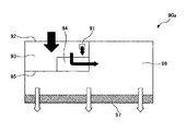
【解決手段】クランプ装置100は、基板収納容器Cの正面に設けられた蓋体68を開閉する際、該基板収納容器に上方から接触して前記基板収納容器を所定位置に固定可能なクランプ部材81と、前記クランプ部材を駆動する駆動機構86、87と、該駆動機構を覆うケーシング85と、該ケーシングと連通する吸い込み口91を有し、該ケーシングの近隣に設けられた排気室90と、該排気室内に設けられたファン94と、を有する。
【選択図】図7
Description
前記クランプ部材を駆動する駆動機構と、
該駆動機構を覆うケーシングと、
該ケーシングと連通する吸い込み口を有し、該ケーシングの近隣に設けられた排気室と、
該排気室内に設けられたファンと、を有する。
該隔壁に設けられた搬送口と、
該搬送口を開閉可能な開閉ドアと、
該搬送口の上方であって、前記隔壁の前記基板収納容器搬送領域側に取り付けられた前記クランプ装置と、
前記搬送口の水平方向両側であって、前記隔壁の前記基板収納容器搬送領域側に設けられた側面カバーと、を有する。
前記基板搬送領域内に設けられた前記基板を搬送する搬送機構と、
前記基板搬送領域内に設けられた処理容器と、を有する。
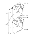
先ず、本発明の実施形態に係るクランプ装置を用いた本発明の実施形態に係る基板処理装置の構成例について説明する。図1に、本発明の実施形態に係る基板処理装置の一例の概略構成図を示す。また、図2に、本発明の実施形態に係る基板処理装置の一例の概略平面図を示す。さらに、図3に、本発明の実施形態に係るキャリア搬送領域の一例の概略斜視図を示す。なお、図2においては、説明のために、図1のロードポート14の一方とFIMSポート24とに、キャリアCが載置されていない状態を示す。
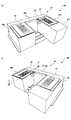
次に、キャリアCの構成について、図4(a)、図4(b)を参照して説明する。
次に、本発明の実施形態に係るクランプ装置100について説明する。
次に、本発明の実施形態に係るクランプ装置100を含む基板搬入出装置と、ウエハ移載機構56とを用いたウエハWの搬送動作について説明する。
次に、図18及び図19を用いて、本発明の実施形態に係るクランプ装置を実施した実施例について説明する。図18は、本発明の実施例に係るクランプ装置のパーティクル測定点を示した図である。図18に示すように、ドア機構の9箇所において、測定点M1〜M9を設定した。そして、本発明の実施例に係るクランプ装置の動作前と動作後におけるパーティクル数を測定した。
4 隔壁
6 搬送口
7 蓋体開閉装置
8 ドア機構
24 FIMSポート
26 熱処理炉
40 フランジ部
41 係合窪み
56 ウエハ移載機構
68 蓋体
80 クランプ機構部
81 クランプ部材
83 ケーシング可動部
84 ケーシング固定部
85 ケーシング
86 駆動部
86a 駆動力発生部
86b シリンダロッド
87 リニアガイド
87a リニアガイド固定部
87b リニアガイド可動部
88 局所排気ダクト
88b 排出口
89 クランプカバー
90、90a〜90c 排気室
91 局所排気吸い込み口
92 内蔵ファン吸い込み口
93 陰圧室
94 ファン
95 仕切
96 陽圧室
97 フィルタ
100 クランプ装置
200 熱処理装置
C キャリア
W ウエハ
Claims (20)
- 基板収納容器の正面に設けられた蓋体を開閉する際、該基板収納容器に上方から接触して前記基板収納容器を所定位置に固定可能なクランプ部材と、
前記クランプ部材を駆動する駆動機構と、
該駆動機構を覆うケーシングと、
該ケーシングと連通する吸い込み口を有し、該ケーシングの近隣に設けられた排気室と、
該排気室内に設けられたファンと、を有するクランプ装置。 - 前記ケーシング内には、前記駆動機構付近に選択的に配置された局所排気ダクトが設けられている請求項1に記載のクランプ装置。
- 前記局所排気ダクトは、前記吸い込み口に連通している請求項2に記載のクランプ装置。
- 前記ケーシングと前記排気室とは隣接しており、前記局所排気ダクトの排出口は前記吸い込み口に直結している請求項2又は3に記載のクランプ装置。
- 前記排気室は、前記ケーシングの両側面に隣接して設けられ、前記ケーシングの両側に前記ファンが設けられた請求項4に記載のクランプ装置。
- 前記ケーシングの両側面に隣接して設けられた前記排気室は、互いに連通している請求項5に記載のクランプ装置。
- 前記ケーシングは、前記クランプ部材に連結され、前記クランプ部材とともに上下動可能な可動部と、前記駆動機構の少なくとも一部及び前記局所排気ダクトを収容する固定部と、を有する請求項2乃至6のいずれか一項に記載のクランプ装置。
- 前記駆動機構は、駆動力を発生させる駆動力発生部と、該駆動力により運動する運動部とを有し、
前記可動部は、前記運動部の少なくとも一部を収容し、
前記固定部は、前記駆動力発生部を収容する請求項7に記載のクランプ装置。 - 前記可動部は、前記固定部の底部の開口に挿入されて設けられ、
該開口の周囲の少なくとも一部には、前記可動部の側面と平行な壁が形成された請求項7又は8に記載のクランプ装置。 - 前記排気室と連続した一体的形状を有し、前記ケーシングを覆うカバー部材を更に有する請求項1乃至9のいずれか一項に記載のクランプ装置。
- 前記ファンは、シロッコファンである請求項1乃至10のいずれか一項に記載のクランプ装置。
- 前記排気室内には清浄フィルタが更に設けられ、
前記吸い込み口から吸い込んだ気体を、該清浄フィルタを介して前記基板収納容器が固定可能な前記所定位置に供給可能である請求項1乃至11のいずれか一項に記載のクランプ装置。 - 前記清浄フィルタは、前記排気室の底面に設けられた請求項12に記載のクランプ装置。
- 前記排気室は、前記ファンが設けられた陰圧室と、前記清浄フィルタが設けられた陽圧室に区分されており、
前記ファンの送風により前記陰圧室に導入された気体が前記陽圧室に送られる請求項12又は13に記載のクランプ装置。 - 前記陰圧室は前記排気室の上面側に設けられるとともに、前記陰圧室の上面には第2の吸い込み口が設けられ、
前記ファンは、該第2の吸い込み口からも気体を吸い込んで前記陽圧室に送風する請求項14に記載のクランプ装置。 - 基板搬送領域と、基板収納容器搬送領域とを区画する隔壁と、
該隔壁に設けられた搬送口と、
該搬送口を開閉可能な開閉ドアと、
該搬送口の上方であって、前記隔壁の前記基板収納容器搬送領域側に取り付けられた請求項1乃至15のいずれか一項に記載のクランプ装置と、
前記搬送口の水平方向両側であって、前記隔壁の前記基板収納容器搬送領域側に設けられた側面カバーと、を有する基板搬入出装置。 - 前記搬送口、前記開閉ドア、前記クランプ装置及び前記側面カバーは、鉛直方向2段で前記隔壁に設けられている請求項16に記載の基板搬入出装置。
- 前記基板搬送領域内に設けられた前記基板収納容器の前記蓋体を開閉する蓋体開閉装置を更に有する請求項16又は17に記載の基板搬入出装置。
- 請求項16乃至18のいずれか一項に記載の基板搬入出装置と、
前記基板搬送領域内に設けられた前記基板を搬送する搬送機構と、
前記基板搬送領域内に設けられた処理容器と、を有する基板処理装置。 - 前記処理容器は、基板を熱処理する熱処理炉である請求項19に記載の基板処理装置。
Priority Applications (5)
| Application Number | Priority Date | Filing Date | Title |
|---|---|---|---|
| JP2015058160A JP6430870B2 (ja) | 2015-03-20 | 2015-03-20 | クランプ装置及びこれを用いた基板搬入出装置、並びに基板処理装置 |
| TW105107695A TWI651802B (zh) | 2015-03-20 | 2016-03-14 | 夾持裝置及使用此夾持裝置之基板運入運出裝置與基板處理裝置 |
| US15/070,123 US9857124B2 (en) | 2015-03-20 | 2016-03-15 | Clamp apparatus, substrate carry-in/out apparatus using the same, and substrate processing apparatus |
| KR1020160031992A KR102053489B1 (ko) | 2015-03-20 | 2016-03-17 | 클램프 장치 및 이것을 이용한 기판 반입출 장치, 및 기판 처리 장치 |
| CN201610157102.3A CN105990196B (zh) | 2015-03-20 | 2016-03-18 | 夹持装置、基板输入输出装置以及基板处理装置 |
Applications Claiming Priority (1)
| Application Number | Priority Date | Filing Date | Title |
|---|---|---|---|
| JP2015058160A JP6430870B2 (ja) | 2015-03-20 | 2015-03-20 | クランプ装置及びこれを用いた基板搬入出装置、並びに基板処理装置 |
Publications (2)
| Publication Number | Publication Date |
|---|---|
| JP2016178232A true JP2016178232A (ja) | 2016-10-06 |
| JP6430870B2 JP6430870B2 (ja) | 2018-11-28 |
Family
ID=56925763
Family Applications (1)
| Application Number | Title | Priority Date | Filing Date |
|---|---|---|---|
| JP2015058160A Active JP6430870B2 (ja) | 2015-03-20 | 2015-03-20 | クランプ装置及びこれを用いた基板搬入出装置、並びに基板処理装置 |
Country Status (5)
| Country | Link |
|---|---|
| US (1) | US9857124B2 (ja) |
| JP (1) | JP6430870B2 (ja) |
| KR (1) | KR102053489B1 (ja) |
| CN (1) | CN105990196B (ja) |
| TW (1) | TWI651802B (ja) |
Families Citing this family (17)
| Publication number | Priority date | Publication date | Assignee | Title |
|---|---|---|---|---|
| JP6430870B2 (ja) * | 2015-03-20 | 2018-11-28 | 東京エレクトロン株式会社 | クランプ装置及びこれを用いた基板搬入出装置、並びに基板処理装置 |
| JP6367763B2 (ja) * | 2015-06-22 | 2018-08-01 | 株式会社荏原製作所 | ウェーハ乾燥装置およびウェーハ乾燥方法 |
| US10109556B2 (en) * | 2016-03-07 | 2018-10-23 | Toyota Motor Engineering & Manufacturing North America, Inc. | Systems and methods for spring-based device attachment |
| US10672639B2 (en) * | 2016-12-07 | 2020-06-02 | Taiwan Semiconductor Manufacturing Co., Ltd. | Method for automatic sending cassette pod |
| TWI621203B (zh) * | 2017-03-22 | 2018-04-11 | 京元電子股份有限公司 | 電子元件定位載具及其推撐設備 |
| CN110612601B (zh) * | 2017-05-11 | 2023-08-22 | 日商乐华股份有限公司 | 薄板状衬底保持指状件以及具有该指状件的运送机器人 |
| CN111052305B (zh) * | 2017-09-06 | 2024-02-02 | 东京毅力科创株式会社 | 半导体制造装置的设置方法和设置系统以及存储介质 |
| JP7109211B2 (ja) | 2018-03-06 | 2022-07-29 | 株式会社Screenホールディングス | 基板処理装置 |
| JP7412137B2 (ja) * | 2019-11-06 | 2024-01-12 | 東京エレクトロン株式会社 | 基板処理装置及び基板収納容器保管方法 |
| JP7469997B2 (ja) * | 2020-09-08 | 2024-04-17 | 株式会社日立ハイテク | 半導体処理装置 |
| CN112151418B (zh) * | 2020-09-11 | 2024-04-05 | 安徽龙芯微科技有限公司 | 一种硅基转接板的封装机构及其封装方法 |
| JP7281519B2 (ja) * | 2021-09-24 | 2023-05-25 | 株式会社Kokusai Electric | 基板処理装置、半導体装置の製造方法および処理容器 |
| CN113758174B (zh) * | 2021-09-30 | 2022-11-04 | 桃源县万羊山生态农业科技发展有限公司 | 一种皇菊加工装置及加工方法 |
| KR102852890B1 (ko) | 2021-10-06 | 2025-09-02 | 삼성전자주식회사 | 기판 이송 장치 |
| CN114823331B (zh) * | 2022-04-22 | 2023-03-03 | 江苏晟驰微电子有限公司 | 一种用于三极管器件制造的氮氢退火设备及其工艺 |
| TWI862112B (zh) * | 2023-08-29 | 2024-11-11 | 日商荏原製作所股份有限公司 | 基板處理裝置 |
| TWI881490B (zh) * | 2023-10-06 | 2025-04-21 | 融程電訊股份有限公司 | 夾持載具 |
Citations (3)
| Publication number | Priority date | Publication date | Assignee | Title |
|---|---|---|---|---|
| JPH10201691A (ja) * | 1997-01-23 | 1998-08-04 | Tsubakimoto Chain Co | クリーンユニットを搭載した天井走行車 |
| JP2006332483A (ja) * | 2005-05-30 | 2006-12-07 | Shimizu Corp | 搬送装置及び搬送装置を使用する方法 |
| JP2014067744A (ja) * | 2012-09-24 | 2014-04-17 | Tokyo Electron Ltd | 搬送装置及び処理装置 |
Family Cites Families (24)
| Publication number | Priority date | Publication date | Assignee | Title |
|---|---|---|---|---|
| US4913790A (en) * | 1988-03-25 | 1990-04-03 | Tokyo Electron Limited | Treating method |
| US5181819A (en) * | 1990-10-09 | 1993-01-26 | Tokyo Electron Sagami Limited | Apparatus for processing semiconductors |
| US5575079A (en) * | 1993-10-29 | 1996-11-19 | Tokyo Electron Limited | Substrate drying apparatus and substrate drying method |
| JP3565577B2 (ja) * | 1994-04-04 | 2004-09-15 | 東京エレクトロン株式会社 | 処理装置 |
| US5628121A (en) * | 1995-12-01 | 1997-05-13 | Convey, Inc. | Method and apparatus for maintaining sensitive articles in a contaminant-free environment |
| JPH10321584A (ja) * | 1997-05-22 | 1998-12-04 | Mitsubishi Electric Corp | 乾燥装置および乾燥方法 |
| JP3897404B2 (ja) * | 1997-07-22 | 2007-03-22 | オメガセミコン電子株式会社 | ベーパ乾燥装置及び乾燥方法 |
| US6319322B1 (en) * | 1998-07-13 | 2001-11-20 | Tokyo Electron Limited | Substrate processing apparatus |
| JP4758846B2 (ja) * | 2005-11-18 | 2011-08-31 | 東京エレクトロン株式会社 | 乾燥装置、乾燥方法、及び乾燥プログラム、並びに、これらを有する基板処理装置、基板処理方法、及び基板処理プログラム |
| JP4527670B2 (ja) * | 2006-01-25 | 2010-08-18 | 東京エレクトロン株式会社 | 加熱処理装置、加熱処理方法、制御プログラムおよびコンピュータ読取可能な記憶媒体 |
| US7654010B2 (en) * | 2006-02-23 | 2010-02-02 | Tokyo Electron Limited | Substrate processing system, substrate processing method, and storage medium |
| US7877895B2 (en) * | 2006-06-26 | 2011-02-01 | Tokyo Electron Limited | Substrate processing apparatus |
| JP4807579B2 (ja) * | 2006-09-13 | 2011-11-02 | 株式会社ダイフク | 基板収納設備及び基板処理設備 |
| JP4327206B2 (ja) * | 2007-01-30 | 2009-09-09 | 東京エレクトロン株式会社 | 縦型熱処理装置及び縦型熱処理方法 |
| JP2008311385A (ja) * | 2007-06-14 | 2008-12-25 | Hitachi High-Technologies Corp | 基板処理装置 |
| JP5184631B2 (ja) * | 2008-06-02 | 2013-04-17 | 東京エレクトロン株式会社 | 流体加熱器、その製造方法、流体加熱器を備えた基板処理装置および基板処理方法 |
| CN102064126B (zh) * | 2010-11-04 | 2013-04-17 | 友达光电股份有限公司 | 基板运输处理方法 |
| JP2012204645A (ja) | 2011-03-25 | 2012-10-22 | Tokyo Electron Ltd | 蓋体開閉装置 |
| JP5603314B2 (ja) * | 2011-12-01 | 2014-10-08 | 東京エレクトロン株式会社 | 搬送装置及び基板処理システム |
| US9644891B2 (en) * | 2012-02-01 | 2017-05-09 | Revive Electronics, LLC | Methods and apparatuses for drying electronic devices |
| JP2015233064A (ja) * | 2014-06-09 | 2015-12-24 | 東京エレクトロン株式会社 | エッチング処理方法及びベベルエッチング装置 |
| US9349620B2 (en) * | 2014-07-09 | 2016-05-24 | Asm Ip Holdings B.V. | Apparatus and method for pre-baking substrate upstream of process chamber |
| JP6385748B2 (ja) * | 2014-07-24 | 2018-09-05 | 東京エレクトロン株式会社 | 熱処理装置及び熱処理方法 |
| JP6430870B2 (ja) * | 2015-03-20 | 2018-11-28 | 東京エレクトロン株式会社 | クランプ装置及びこれを用いた基板搬入出装置、並びに基板処理装置 |
-
2015
- 2015-03-20 JP JP2015058160A patent/JP6430870B2/ja active Active
-
2016
- 2016-03-14 TW TW105107695A patent/TWI651802B/zh active
- 2016-03-15 US US15/070,123 patent/US9857124B2/en active Active
- 2016-03-17 KR KR1020160031992A patent/KR102053489B1/ko active Active
- 2016-03-18 CN CN201610157102.3A patent/CN105990196B/zh active Active
Patent Citations (3)
| Publication number | Priority date | Publication date | Assignee | Title |
|---|---|---|---|---|
| JPH10201691A (ja) * | 1997-01-23 | 1998-08-04 | Tsubakimoto Chain Co | クリーンユニットを搭載した天井走行車 |
| JP2006332483A (ja) * | 2005-05-30 | 2006-12-07 | Shimizu Corp | 搬送装置及び搬送装置を使用する方法 |
| JP2014067744A (ja) * | 2012-09-24 | 2014-04-17 | Tokyo Electron Ltd | 搬送装置及び処理装置 |
Also Published As
| Publication number | Publication date |
|---|---|
| US9857124B2 (en) | 2018-01-02 |
| KR102053489B1 (ko) | 2019-12-06 |
| CN105990196B (zh) | 2020-04-07 |
| CN105990196A (zh) | 2016-10-05 |
| TW201705356A (zh) | 2017-02-01 |
| TWI651802B (zh) | 2019-02-21 |
| JP6430870B2 (ja) | 2018-11-28 |
| US20160273836A1 (en) | 2016-09-22 |
| KR20160113013A (ko) | 2016-09-28 |
Similar Documents
| Publication | Publication Date | Title |
|---|---|---|
| JP6430870B2 (ja) | クランプ装置及びこれを用いた基板搬入出装置、並びに基板処理装置 | |
| JP6198043B2 (ja) | ロードポートユニット及びefemシステム | |
| JP6679906B2 (ja) | Efem | |
| CN107039322B (zh) | 微环境装置 | |
| CN102683246B (zh) | 盖体开闭装置 | |
| CN106876310B (zh) | Efem中的晶圆搬运部及装载端口部的控制方法 | |
| JP7496493B2 (ja) | 搬送ロボット、及びefem | |
| JPWO2020111013A1 (ja) | ウェーハストッカ | |
| JP5048590B2 (ja) | 基板処理装置 | |
| JP4541232B2 (ja) | 処理システム及び処理方法 | |
| CN111755367B (zh) | 基板处理装置 | |
| CN107017190B (zh) | 装载端口装置及向装载端口装置的容器内的清洁化气体导入方法 | |
| JP2016066689A (ja) | 容器清掃装置及び容器清掃方法 | |
| JP2016063081A (ja) | 蓋体開閉装置及び蓋体開閉方法 | |
| JP4790326B2 (ja) | 処理システム及び処理方法 | |
| JP7081119B2 (ja) | ロードポート装置 | |
| WO2003088351A1 (fr) | Structure d'orifice dans un dispositif de traitement de semi-conducteur | |
| JP6374775B2 (ja) | 基板搬送システム及びこれを用いた熱処理装置 | |
| JP2005347667A (ja) | 半導体製造装置 | |
| JP2000091399A (ja) | 半導体製造装置 | |
| KR20010002584A (ko) | 오염 입자 제거 기능을 갖는 스탠더드 메커니컬 인터페이스 시스템 |
Legal Events
| Date | Code | Title | Description |
|---|---|---|---|
| A621 | Written request for application examination |
Free format text: JAPANESE INTERMEDIATE CODE: A621 Effective date: 20170913 |
|
| A977 | Report on retrieval |
Free format text: JAPANESE INTERMEDIATE CODE: A971007 Effective date: 20180412 |
|
| A131 | Notification of reasons for refusal |
Free format text: JAPANESE INTERMEDIATE CODE: A131 Effective date: 20180417 |
|
| A521 | Request for written amendment filed |
Free format text: JAPANESE INTERMEDIATE CODE: A523 Effective date: 20180613 |
|
| TRDD | Decision of grant or rejection written | ||
| A01 | Written decision to grant a patent or to grant a registration (utility model) |
Free format text: JAPANESE INTERMEDIATE CODE: A01 Effective date: 20181009 |
|
| A61 | First payment of annual fees (during grant procedure) |
Free format text: JAPANESE INTERMEDIATE CODE: A61 Effective date: 20181101 |
|
| R150 | Certificate of patent or registration of utility model |
Ref document number: 6430870 Country of ref document: JP Free format text: JAPANESE INTERMEDIATE CODE: R150 |
|
| R250 | Receipt of annual fees |
Free format text: JAPANESE INTERMEDIATE CODE: R250 |
|
| R250 | Receipt of annual fees |
Free format text: JAPANESE INTERMEDIATE CODE: R250 |
|
| R250 | Receipt of annual fees |
Free format text: JAPANESE INTERMEDIATE CODE: R250 |
|
| R250 | Receipt of annual fees |
Free format text: JAPANESE INTERMEDIATE CODE: R250 |
|
| R250 | Receipt of annual fees |
Free format text: JAPANESE INTERMEDIATE CODE: R250 |