JP2016219782A - Stretchable flexible substrate and manufacturing method thereof - Google Patents
Stretchable flexible substrate and manufacturing method thereof Download PDFInfo
- Publication number
- JP2016219782A JP2016219782A JP2016058851A JP2016058851A JP2016219782A JP 2016219782 A JP2016219782 A JP 2016219782A JP 2016058851 A JP2016058851 A JP 2016058851A JP 2016058851 A JP2016058851 A JP 2016058851A JP 2016219782 A JP2016219782 A JP 2016219782A
- Authority
- JP
- Japan
- Prior art keywords
- insulating layer
- layer
- flexible substrate
- metal layer
- stretchable flexible
- Prior art date
- Legal status (The legal status is an assumption and is not a legal conclusion. Google has not performed a legal analysis and makes no representation as to the accuracy of the status listed.)
- Granted
Links
Images














Classifications
-
- H—ELECTRICITY
- H05—ELECTRIC TECHNIQUES NOT OTHERWISE PROVIDED FOR
- H05K—PRINTED CIRCUITS; CASINGS OR CONSTRUCTIONAL DETAILS OF ELECTRIC APPARATUS; MANUFACTURE OF ASSEMBLAGES OF ELECTRICAL COMPONENTS
- H05K1/00—Printed circuits
- H05K1/02—Details
- H05K1/0277—Bendability or stretchability details
- H05K1/0283—Stretchable printed circuits
-
- H—ELECTRICITY
- H05—ELECTRIC TECHNIQUES NOT OTHERWISE PROVIDED FOR
- H05K—PRINTED CIRCUITS; CASINGS OR CONSTRUCTIONAL DETAILS OF ELECTRIC APPARATUS; MANUFACTURE OF ASSEMBLAGES OF ELECTRICAL COMPONENTS
- H05K1/00—Printed circuits
- H05K1/02—Details
- H05K1/0277—Bendability or stretchability details
- H05K1/028—Bending or folding regions of flexible printed circuits
-
- H—ELECTRICITY
- H05—ELECTRIC TECHNIQUES NOT OTHERWISE PROVIDED FOR
- H05K—PRINTED CIRCUITS; CASINGS OR CONSTRUCTIONAL DETAILS OF ELECTRIC APPARATUS; MANUFACTURE OF ASSEMBLAGES OF ELECTRICAL COMPONENTS
- H05K1/00—Printed circuits
- H05K1/18—Printed circuits structurally associated with non-printed electric components
- H05K1/182—Printed circuits structurally associated with non-printed electric components associated with components mounted in printed circuit boards [PCB], e.g. insert-mounted components [IMC]
- H05K1/185—Printed circuits structurally associated with non-printed electric components associated with components mounted in printed circuit boards [PCB], e.g. insert-mounted components [IMC] associated with components encapsulated in the insulating substrate of the PCBs; associated with components incorporated in internal layers of multilayer circuit boards
-
- H—ELECTRICITY
- H05—ELECTRIC TECHNIQUES NOT OTHERWISE PROVIDED FOR
- H05K—PRINTED CIRCUITS; CASINGS OR CONSTRUCTIONAL DETAILS OF ELECTRIC APPARATUS; MANUFACTURE OF ASSEMBLAGES OF ELECTRICAL COMPONENTS
- H05K3/00—Apparatus or processes for manufacturing printed circuits
- H05K3/10—Apparatus or processes for manufacturing printed circuits in which conductive material is applied to the insulating support in such a manner as to form the desired conductive pattern
- H05K3/18—Apparatus or processes for manufacturing printed circuits in which conductive material is applied to the insulating support in such a manner as to form the desired conductive pattern using precipitation techniques to apply the conductive material
-
- H—ELECTRICITY
- H05—ELECTRIC TECHNIQUES NOT OTHERWISE PROVIDED FOR
- H05K—PRINTED CIRCUITS; CASINGS OR CONSTRUCTIONAL DETAILS OF ELECTRIC APPARATUS; MANUFACTURE OF ASSEMBLAGES OF ELECTRICAL COMPONENTS
- H05K2201/00—Indexing scheme relating to printed circuits covered by H05K1/00
- H05K2201/05—Flexible printed circuits [FPCs]
- H05K2201/055—Folded back on itself
-
- H—ELECTRICITY
- H05—ELECTRIC TECHNIQUES NOT OTHERWISE PROVIDED FOR
- H05K—PRINTED CIRCUITS; CASINGS OR CONSTRUCTIONAL DETAILS OF ELECTRIC APPARATUS; MANUFACTURE OF ASSEMBLAGES OF ELECTRICAL COMPONENTS
- H05K2201/00—Indexing scheme relating to printed circuits covered by H05K1/00
- H05K2201/10—Details of components or other objects attached to or integrated in a printed circuit board
- H05K2201/10007—Types of components
- H05K2201/10151—Sensor
Landscapes
- Engineering & Computer Science (AREA)
- Microelectronics & Electronic Packaging (AREA)
- Manufacturing & Machinery (AREA)
- Structure Of Printed Boards (AREA)
- Laminated Bodies (AREA)
- Non-Metallic Protective Coatings For Printed Circuits (AREA)
- Structures For Mounting Electric Components On Printed Circuit Boards (AREA)
Abstract
【課題】伸縮性基板にとって好適な技術を提供すること。【解決手段】本開示の一態様に係る伸縮性フレキシブル基板は、電子部品、前記電子部品の周囲に位置付けられ、互いに対向する第1主面および第2主面を有する第1絶縁層、前記第1主面と接する第1金属層、前記第2主面と接し、前記電子部品と電気的に接続された第2金属層、ならびに前記電子部品、前記第1絶縁層および前記第2金属層を封止する第2絶縁層を備え、平面視において、少なくとも前記電子部品と、前記第1絶縁層の一部と、前記第1金属層の一部と、前記第2金属層の一部とから構成される中心部から、少なくとも前記第1絶縁層の前記一部以外の他部と、前記第1金属層の前記一部以外の他部と、前記第2金属層の前記一部以外の他部とから構成される少なくとも1つの湾曲配線部が延びており、前記少なくとも1つの湾曲配線部は、少なくとも部分的に湾曲している。【選択図】図1A technique suitable for a stretchable substrate is provided. A stretchable flexible substrate according to an aspect of the present disclosure includes an electronic component, a first insulating layer positioned around the electronic component and having a first main surface and a second main surface facing each other, the first A first metal layer in contact with one main surface; a second metal layer in contact with the second main surface and electrically connected to the electronic component; and the electronic component, the first insulating layer, and the second metal layer. A second insulating layer for sealing; and in plan view, from at least the electronic component, a part of the first insulating layer, a part of the first metal layer, and a part of the second metal layer Other than at least the other part other than the part of the first insulating layer, the other part other than the part of the first metal layer, and the other part other than the part of the second metal layer. Extending at least one curved wiring portion, the at least one One of the curved line portion is at least partially curved. [Selection] Figure 1
Description
本開示は、伸縮性フレキシブル基板およびその製造方法に関する。 The present disclosure relates to a stretchable flexible substrate and a manufacturing method thereof.
近年、電子デバイスの小型化・薄型化に伴い、可撓性を有したフレキシブル基板が多く用いられている。フレキシブル特性を有する基板は、従前より小型化が求められているモバイル機器の他、種々の機器での利用が検討されている。例えば、ユーザーの動きに追従するようなフレキシブル特性を要するウェアラブル機器等での利用が検討されている。 In recent years, with the miniaturization and thinning of electronic devices, flexible flexible substrates are often used. Substrates having flexible properties are being studied for use in various devices in addition to mobile devices that have been required to be smaller in the past. For example, use in a wearable device or the like that requires a flexible characteristic to follow a user's movement is being studied.
想定されるウェアラブル機器としては、人体に密着することで高精度なセンシングが可能なセンサデバイス、並びに、人体の動きおよび三次元の凹凸に追従する表示デバイスなどが挙げられる。このようなデバイスでは人体の関節および可動部に無理なく装着することが求められ、ユーザーの動きにフィットした装着感およびデザイン等が重視される。従って、ウェアラブル機器に展開するフレキシブル基板に対しては、可撓性に加えて、伸縮性をも備えていることが要求される。 Possible wearable devices include a sensor device capable of highly accurate sensing by being in close contact with the human body, and a display device that follows the movement of the human body and three-dimensional unevenness. In such a device, it is required to comfortably attach it to a joint and a movable part of a human body, and importance is attached to a wearing feeling and a design that fit the user's movement. Therefore, it is required for a flexible substrate developed in a wearable device to have stretchability in addition to flexibility.
本願発明者らは、鋭意検討の末、従来のフレキシブル基板について更なる改善点があることを今回見出した。具体的には、フレキシブル基板に対して積極的に伸縮性を持たせようとすると、“伸縮性”ゆえの特有の問題が引き起こされ得ることが分かった。特に伸縮性基板を製造するに際しては、“伸縮性”ゆえの特有の困難を伴うことが多く、例えば部品実装などの点で困難を伴い得る。 The inventors of the present application have now found that there is a further improvement with respect to the conventional flexible substrate after extensive studies. Specifically, it has been found that if the flexible substrate is positively stretchable, a specific problem due to “stretchability” may be caused. In particular, when a stretchable substrate is manufactured, there are many cases where there is a particular difficulty due to “stretchability”, which can be difficult in terms of component mounting, for example.
そこで、本開示の主たる目的は、伸縮性基板にとって好適な技術を提供することである。 Therefore, a main object of the present disclosure is to provide a technique suitable for the stretchable substrate.
本開示の一態様に係る伸縮性フレキシブル基板は、電子部品、前記電子部品の周囲に位置付けられ、互いに対向する第1主面および第2主面を有する第1絶縁層、前記第1主面と接する第1金属層、前記第2主面と接し、前記電子部品と電気的に接続された第2金属層、ならびに前記電子部品、前記第1絶縁層および前記第2金属層を封止する第2絶縁層を備え、平面視において、少なくとも前記電子部品と、前記第1絶縁層の一部と、前記第1金属層の一部と、前記第2金属層の一部とから構成される中心部から、少なくとも前記第1絶縁層の前記一部以外の他部と、前記第1金属層の前記一部以外の他部と、前記第2金属層の前記一部以外の他部とから構成される少なくとも1つの湾曲配線部が延びており、前記少なくとも1つの湾曲配線部は、少なくとも部分的に湾曲している。 A stretchable flexible substrate according to an aspect of the present disclosure includes an electronic component, a first insulating layer that is positioned around the electronic component and has a first main surface and a second main surface that face each other, the first main surface, A first metal layer contacting the second metal layer in contact with the second main surface and electrically connected to the electronic component; and a first metal layer sealing the electronic component, the first insulating layer, and the second metal layer. A center including at least the electronic component, a part of the first insulating layer, a part of the first metal layer, and a part of the second metal layer in a plan view. From at least another part other than the part of the first insulating layer, another part other than the part of the first metal layer, and another part other than the part of the second metal layer. At least one curved wiring portion extending, and the at least one curved wiring portion extends. Parts are at least partially curved.
本開示は、伸縮性フレキシブル基板に好適な技術を供している。具体的には、本開示の一態様に係る伸縮性フレキシブル基板では、その製造に伴った困難さが低減されており、例えば部品実装などの点で困難さが低減されている。 The present disclosure provides a technique suitable for a stretchable flexible substrate. Specifically, in the stretchable flexible substrate according to one aspect of the present disclosure, the difficulty associated with its manufacture is reduced, and the difficulty is reduced in terms of component mounting, for example.
(本開示の基礎となった知見)
本願発明者らは、従来のフレキシブル基板について更なる改善点があることを見出し、本開示を案出した。具体的には、フレキシブル基板に対して積極的に伸縮性を持たせようとすると、“伸縮性”ゆえの特有の懸念が生じ得ることを見出した。特に伸縮性基板を製造するに際しては、それ特有の困難を伴うことがあり、例えば部品実装などの点で困難を伴い得る。
(Knowledge that became the basis of this disclosure)
The inventors of the present application have found that there are further improvements with respect to the conventional flexible substrate, and have devised the present disclosure. Specifically, it has been found that if the flexible substrate is positively stretchable, there may be a particular concern due to “stretchability”. In particular, when a stretchable substrate is manufactured, there may be a difficulty peculiar to that, for example, it may be difficult in terms of component mounting.
従前に提案されたフレキシブル基板は、“伸縮性”の要求に応えるために、可撓性を有し、かつ、配線部を蛇行状の形態を成すように構成されたものとなっていた。しかしながら、かかるフレキシブル基板は、屈曲した形態の配線部を用いて構成しているので基板の伸縮時に応力が屈曲部に集中し易い。そのため、伸縮が繰り返されると、配線部で破断するおそれがある。又、そのようなフレキシブル基板は、フレキシブル基板の延在方向に伸縮可能である一方、当該延在方向と異なる方向には伸縮しにくい。それゆえ、従前に提案されたフレキシブル基板は、可撓性を有するものの、ウェアラブル機器として十分な伸縮性を有しているとは言い難い。 Previously proposed flexible substrates have been configured to have flexibility and have a wiring portion in a meandering form in order to meet the demand for “stretchability”. However, since such a flexible substrate is configured using a bent wiring portion, stress tends to concentrate on the bent portion when the substrate expands and contracts. Therefore, if expansion and contraction is repeated, there is a risk of breaking at the wiring portion. Further, such a flexible substrate can be expanded and contracted in the extending direction of the flexible substrate, but is not easily expanded and contracted in a direction different from the extending direction. Therefore, although the previously proposed flexible substrate has flexibility, it cannot be said that it has sufficient stretchability as a wearable device.
また、従前のフレキシブル基板は、その製法の点でも制約が比較的大きい。具体的には、基板の伸縮性の向上のため、より伸縮性の高い材料を用いて作製することになるが、用いられる材料に対しては、部品実装工程に鑑みてリフロー温度以上の耐熱性が求められる。また、基板に電子部品を実装する際には、“伸縮”ゆえに、設計した部品位置とズレが生じる場合があり、微細な部品実装などが困難となり得るといった懸念もある。 Further, the conventional flexible substrate is relatively limited in terms of its manufacturing method. Specifically, in order to improve the stretchability of the board, it will be manufactured using a material with higher stretchability, but for the material used, heat resistance above the reflow temperature in view of the component mounting process Is required. In addition, when electronic components are mounted on a substrate, there is a possibility that deviation from the designed component position may occur due to “extension and contraction”, which may make it difficult to mount fine components.
本開示は、以下の項目に記載の伸縮性フレキシブル基板およびその製造方法を含む。
[項目1]
電子部品、
前記電子部品の周囲に位置付けられ、互いに対向する第1主面および第2主面を有する第1絶縁層、
前記第1主面と接する第1金属層、
前記第2主面と接し、前記電子部品と電気的に接続された第2金属層、ならびに
前記電子部品、前記第1絶縁層および前記第2金属層を封止する第2絶縁層
を備え、
平面視において、
少なくとも前記電子部品と、前記第1絶縁層の一部と、前記第1金属層の一部と、前記第2金属層の一部とから構成される中心部から、
少なくとも前記第1絶縁層の前記一部以外の他部と、前記第1金属層の前記一部以外の他部と、前記第2金属層の前記一部以外の他部とから構成される少なくとも1つの湾曲配線部が延びており、
前記少なくとも1つの湾曲配線部は、少なくとも部分的に湾曲している、伸縮性フレキシブル基板。
本開示の一態様に係る伸縮性フレキシブル基板において、前記少なくとも1つの湾曲配線部が、複数の湾曲配線部を含んでいてもよい。
[項目2]
前記少なくとも1つの湾曲配線部の曲率の変化に起因して前記伸縮性フレキシブル基板が伸縮自在となっている、項目1に記載の伸縮性フレキシブル基板。
[項目3]
前記中心部では、前記電子部品が前記第1絶縁層の前記一部に囲まれている、項目1または2に記載の伸縮性フレキシブル基板。
[項目4]
前記電子部品と前記第1金属層との間に、前記電子部品と接する接着剤層を更に備える、項目1から3のいずれかに記載の伸縮性フレキシブル基板。
[項目5]
前記第1金属層が金属箔である、項目1から4のいずれかに記載の伸縮性フレキシブル基板。
[項目6]
前記第1絶縁層および前記第2絶縁層がいずれも樹脂層であり、
前記第2絶縁層が前記第1絶縁層よりも軟質である、項目1から5のいずれかに記載の伸縮性フレキシブル基板。
[項目7]
前記第1金属層を封止する第3絶縁層を更に備え、
前記第2絶縁層と前記第3絶縁層とが互いに積層されている、項目1から6のいずれかに記載の伸縮性フレキシブル基板。
[項目8]
前記第1金属層が、前記第2絶縁層と前記第3絶縁層との界面に対して面一である、項目7に記載の伸縮性フレキシブル基板。
[項目9]
前記第1絶縁層が、前記第2絶縁層と前記第3絶縁層との界面に対して面一である、項目7または8に記載の伸縮性フレキシブル基板。
[項目10]
前記第1金属層を封止する第3絶縁層を更に備え、
前記第2絶縁層と前記第3絶縁層とが互いに積層されており、
前記接着剤層が、前記第2絶縁層と前記第3絶縁層との界面に対して面一である、項目4に記載の伸縮性フレキシブル基板。
[項目11]
前記第1絶縁層および前記第3絶縁層がいずれも樹脂層であり、
前記第3絶縁層が前記第1絶縁層よりも軟質である、項目7から10のいずれかに記載の伸縮性フレキシブル基板。
[項目12]
前記第1絶縁層を貫通する間隙を更に備え、
前記間隙を通して、前記第1金属層と前記第2金属層とを電気的に接続されている、項目1から11のいずれかに記載の伸縮性フレキシブル基板。
[項目13]
前記間隙が前記第2金属層により満たされている、項目12に記載の伸縮性フレキシブル基板。
[項目14]
(i)第1金属層の前駆部材上に、中空領域を有すると共に前記中空領域を中心として湾曲するように延在する少なくとも1つの湾曲部を有する第1絶縁層を設ける工程、
(ii)前記中空領域に電子部品を配置する工程、
(iii)めっき処理を実施し、前記めっき処理によって形成されためっき層に対して第1パターニング処理を実施して第2金属層を形成する工程、
(iv)前記電子部品、前記第1絶縁層および前記第2金属層を封止するように前記前駆部材上に第2絶縁層を形成する工程、および
(v)前記前駆部材を第2パターニング処理して第1金属層を得る工程
を含む、伸縮性フレキシブル基板の製造方法。
本開示の一態様に係る伸縮性フレキシブル基板の製造方法において、前記少なくとも1つの湾曲部が、複数の湾曲部を含んでいてもよい。
[項目15]
前記工程(i)の前記前駆部材として金属箔を用いる、項目14に記載の伸縮性フレキシブル基板の製造方法。
[項目16]
前記第1絶縁層および前記第2絶縁層をそれぞれ樹脂層として形成し、
前記第2絶縁層を前記第1絶縁層よりも軟質の樹脂材を用いて形成する、項目14または15に記載の伸縮性フレキシブル基板の製造方法。
[項目17]
前記工程(v)の後に、前記第1金属層を封止するように第3絶縁層を形成する工程を更に含む、項目14から16のいずれかに記載の伸縮性フレキシブル基板の製造方法。
[項目18]
前記第1絶縁層および前記第3絶縁層をそれぞれ樹脂層として形成し、
前記第3絶縁層を前記第1絶縁層よりも軟質の樹脂材を用いて形成する、項目17に記載の伸縮性フレキシブル基板の製造方法。
[項目19]
前記工程(ii)では、前記中空領域に接着剤層を形成した後、前記接着剤層と接するように前記電子部品を配置する、項目14から18のいずれかに記載の伸縮性フレキシブル基板の製造方法。
[項目20]
前記工程(iii)の前記めっき処理として、乾式めっき法を実施した後で湿式めっき法を実施する、項目14から19のいずれかに記載の伸縮性フレキシブル基板の製造方法。
[項目21]
前記工程(iii)では、前記少なくとも1つの湾曲部に起因してもたらされる前記第1絶縁層の間隙を満たすように前記第2金属層を形成することにより、前記間隙において前記第1金属層と前記第2金属層とが接続される、項目14から20のいずれかに記載の伸縮性フレキシブル基板の製造方法。
[項目22]
前記工程(iv)に先立って、前記工程(v)を実施する、項目14から21のいずれかに記載の伸縮性フレキシブル基板の製造方法。
[項目23]
前記工程(iii)の前記第1パターニング処理と、前記工程(v)の前記第2パターニング処理とを一括して実施する、項目22に記載の伸縮性フレキシブル基板の製造方法。
The present disclosure includes the stretchable flexible substrate and the manufacturing method thereof described in the following items.
[Item 1]
Electronic components,
A first insulating layer positioned around the electronic component and having a first main surface and a second main surface facing each other;
A first metal layer in contact with the first main surface;
A second metal layer in contact with the second main surface and electrically connected to the electronic component; and a second insulating layer for sealing the electronic component, the first insulating layer and the second metal layer,
In plan view,
From a central portion constituted by at least the electronic component, a part of the first insulating layer, a part of the first metal layer, and a part of the second metal layer,
At least other parts other than the part of the first insulating layer, other parts other than the part of the first metal layer, and other parts other than the part of the second metal layer. One curved wiring part extends,
The stretchable flexible substrate, wherein the at least one curved wiring portion is at least partially curved.
In the stretchable flexible substrate according to one aspect of the present disclosure, the at least one curved wiring portion may include a plurality of curved wiring portions.
[Item 2]
The stretchable flexible substrate according to
[Item 3]
3. The stretchable flexible substrate according to
[Item 4]
4. The stretchable flexible substrate according to any one of
[Item 5]
5. The stretchable flexible substrate according to any one of
[Item 6]
The first insulating layer and the second insulating layer are both resin layers,
The stretchable flexible substrate according to any one of
[Item 7]
A third insulating layer for sealing the first metal layer;
The stretchable flexible substrate according to any one of
[Item 8]
The stretchable flexible substrate according to
[Item 9]
Item 9. The stretchable flexible substrate according to
[Item 10]
A third insulating layer for sealing the first metal layer;
The second insulating layer and the third insulating layer are stacked on each other;
[Item 11]
The first insulating layer and the third insulating layer are both resin layers,
The stretchable flexible substrate according to any one of
[Item 12]
A gap penetrating the first insulating layer;
The stretchable flexible substrate according to any one of
[Item 13]
13. The stretchable flexible substrate according to
[Item 14]
(I) providing a first insulating layer having a hollow region and at least one curved portion extending around the hollow region on the precursor member of the first metal layer;
(Ii) a step of arranging an electronic component in the hollow region;
(Iii) performing a plating process and performing a first patterning process on the plating layer formed by the plating process to form a second metal layer;
(Iv) forming a second insulating layer on the precursor member so as to seal the electronic component, the first insulating layer, and the second metal layer; and (v) performing a second patterning process on the precursor member. And the manufacturing method of a stretchable flexible substrate including the process of obtaining a 1st metal layer.
In the method for manufacturing a stretchable flexible substrate according to one aspect of the present disclosure, the at least one curved portion may include a plurality of curved portions.
[Item 15]
Item 15. The method for producing a stretchable flexible substrate according to Item 14, wherein a metal foil is used as the precursor member in the step (i).
[Item 16]
Forming each of the first insulating layer and the second insulating layer as a resin layer;
Item 16. The method for producing a stretchable flexible substrate according to Item 14 or 15, wherein the second insulating layer is formed using a softer resin material than the first insulating layer.
[Item 17]
The method for producing a stretchable flexible substrate according to any one of items 14 to 16, further comprising a step of forming a third insulating layer so as to seal the first metal layer after the step (v).
[Item 18]
Forming each of the first insulating layer and the third insulating layer as a resin layer;
Item 18. The method for manufacturing a stretchable flexible substrate according to Item 17, wherein the third insulating layer is formed using a resin material softer than the first insulating layer.
[Item 19]
In the said process (ii), after forming an adhesive bond layer in the said hollow area | region, the said electronic component is arrange | positioned so that the said adhesive bond layer may be contacted, The manufacture of the elastic flexible board | substrate in any one of the items 14-18 Method.
[Item 20]
20. The method for producing a stretchable flexible substrate according to any one of items 14 to 19, wherein a wet plating method is performed after a dry plating method is performed as the plating treatment in the step (iii).
[Item 21]
In the step (iii), the second metal layer is formed so as to fill a gap of the first insulating layer caused by the at least one curved portion, so that the first metal layer and the first metal layer are formed in the gap. Item 21. The method for producing a stretchable flexible substrate according to any one of Items 14 to 20, wherein the second metal layer is connected.
[Item 22]
Item 22. The method for producing a stretchable flexible substrate according to any one of Items 14 to 21, wherein the step (v) is performed prior to the step (iv).
[Item 23]
Item 23. The method for manufacturing a stretchable flexible substrate according to Item 22, wherein the first patterning process in the step (iii) and the second patterning process in the step (v) are collectively performed.
かかる本開示の一態様に係る伸縮性フレキシブル基板の特徴の1つは、電子部品の周囲に位置付けられた絶縁層の両面にそれぞれ接するように第1金属層と第2金属層とが設けられており、かかる絶縁層、電子部品および第2金属層を封止する更なる絶縁層が設けられていることである。 One of the features of the stretchable flexible substrate according to one aspect of the present disclosure is that the first metal layer and the second metal layer are provided so as to be in contact with both surfaces of the insulating layer positioned around the electronic component, respectively. And a further insulating layer for sealing the insulating layer, the electronic component, and the second metal layer is provided.
かかる本開示の一態様に係る伸縮性フレキシブル基板の製造方法の特徴の1つは、第1金属層の前駆部材上にて特異な形態の第1絶縁層を形成すること、およびそれに関連して実施される以降の工程に存する。具体的には、中空領域およびその中空領域を中心として湾曲するように延在する湾曲部を有する第1絶縁層を第1金属層の前駆部材上に設けること、およびそのような第1金属層の前駆部材および第1絶縁層に対して施されるその後の工程に特徴がある。 One of the features of the method for manufacturing a stretchable flexible substrate according to one aspect of the present disclosure is to form a unique insulating first layer on a precursor member of the first metal layer, and related thereto. It exists in the subsequent process. Specifically, a first insulating layer having a hollow region and a curved portion extending so as to bend around the hollow region is provided on the precursor member of the first metal layer, and such a first metal layer is provided. The precursor member and the subsequent process applied to the first insulating layer are characterized.
上述したような本開示は、伸縮性フレキシブル基板の好適な実現に資する。具体的には、蛇行状に折り畳むように構成された従前のフレキシブル基板は、蛇行形状が引き伸ばされた時に、応力が折り曲げ部の一点に集中し、銅箔パターンの破断の原因となっていたのに対し、本開示の一態様に係る伸縮性フレキシブル基板では引き伸ばされると、湾曲配線部の巻回状態が外周からほどけるように変化するので、特定の一点に応力が集中することがなく無理なく基板が伸張される。さらに配線伸縮の伸び率についても、湾曲配線部の巻回数を増やすことで大きな伸び率を稼ぐことができる。 The present disclosure as described above contributes to a suitable realization of the stretchable flexible substrate. Specifically, the conventional flexible substrate configured to fold in a meandering manner caused stress to concentrate on one point of the bent portion when the meandering shape was stretched, causing the copper foil pattern to break. On the other hand, when the stretchable flexible substrate according to one aspect of the present disclosure is stretched, the winding state of the curved wiring portion changes so as to be unwound from the outer periphery, so that stress is not concentrated on a specific point without difficulty. The substrate is stretched. Further, the elongation rate of the wiring expansion / contraction can be increased by increasing the number of turns of the curved wiring portion.
また、本開示の一態様に係る伸縮性フレキシブル基板の製造方法では、伸縮性フレキシブル基板の製造に伴った困難さが低減されており、例えば部品実装などの点で困難さが低減されている。より具体的には、電子部品の実装において実装箇所に「“凹部”に相当する“中空領域”」が形成されていることで実装工程の位置ずれが低減し、部品脱落を抑制することができる。換言すれば、本開示の一態様に係る製造方法は、製造時における電子部品の脱落・位置ずれを防止することが可能であり、信頼性の高い伸縮性フレキシブル基板の製造に資するといえる。 Further, in the method for manufacturing a stretchable flexible substrate according to one aspect of the present disclosure, the difficulty associated with the manufacture of the stretchable flexible substrate is reduced. For example, the difficulty is reduced in terms of component mounting. More specifically, the “hollow region” corresponding to the “recess” is formed at the mounting position in mounting the electronic component, so that the positional deviation in the mounting process can be reduced and the component can be prevented from falling off. . In other words, it can be said that the manufacturing method according to one embodiment of the present disclosure can prevent the electronic component from dropping or misaligned during manufacturing, and contributes to the manufacture of a highly reliable flexible flexible substrate.
更にいえば、従前のフレキシブル基板ではリフロー工程での温度以上の耐熱性を有する材料しか使えなかったが、本開示の一態様に係る伸縮性フレキシブル基板の製造方法ではそのような材料の制約が減じられている。具体的には、本開示の一態様に係る伸縮性フレキシブル基板の製造方法では、半田接続を特に用いる必要が無く、それゆえ、リフロー耐熱性を特に有さない材料であっても使用できる。 Furthermore, the conventional flexible substrate can only use a material having a heat resistance equal to or higher than the temperature in the reflow process, but the elastic flexible substrate manufacturing method according to one embodiment of the present disclosure reduces such material restrictions. It has been. Specifically, in the method for manufacturing a stretchable flexible substrate according to one embodiment of the present disclosure, it is not particularly necessary to use solder connection, and thus even a material that does not particularly have reflow heat resistance can be used.
以下にて、本開示の一態様に係る伸縮性フレキシブル基板およびその製造方法を詳細に説明する。尚、図面に示す各種の要素は、本開示の理解のために模式的に示したにすぎず、寸法比および外観などは実物と異なり得ることに留意されたい。 Hereinafter, the stretchable flexible substrate and the manufacturing method thereof according to one embodiment of the present disclosure will be described in detail. It should be noted that the various elements shown in the drawings are merely schematically shown for understanding of the present disclosure, and the dimensional ratio, appearance, and the like may be different from the actual ones.
[本開示のフレキシブル基板]
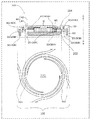
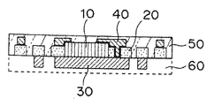
図1に、本開示の伸縮性フレキシブル基板の構成を模式的に示す。図示されるように、本開示の伸縮性フレキシブル基板100は、電子部品10、第1絶縁層20、第1金属層30、第2金属層40、および、第2絶縁層50を備える。
[Flexible substrate of the present disclosure]
FIG. 1 schematically shows the configuration of the stretchable flexible substrate of the present disclosure. As illustrated, the stretchable
第1絶縁層20は、電子部品10の周囲に位置付けられ、互いに対向する第1主面202および第2主面204を有している。第1金属層30は、第1絶縁層20の第1主面202と接するように設けられている。一方、第2金属層40は、第1絶縁層20の第2主面204と接するように設けられ、電子部品10と電気的に接続して設けられている。図示する態様でいえば、第1絶縁層20の下側主面上に第1金属層30が設けられている一方、第1絶縁層20の上側主面上に第2金属層40が設けられている。第2絶縁層50は、電子部品10、第1絶縁層20および第2金属層40を封止するように設けられている。
The first insulating
本開示の伸縮性フレキシブル基板100は、各種の構成要素が“伸縮性”を発現すべく互いに好適な積層関係・配置関係を有している。つまり、電子部品10、第1絶縁層20、第1金属層30、第2金属層40および第2絶縁層50が互いに好適に配置・積層された構成となっている。
The stretchable
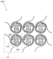
本開示の伸縮性フレキシブル基板100は、あくまでも、“伸縮性”を呈するものであり、図1に示す態様から分かるように、全体的として渦巻き状の形態を少なくとも1つ有している。つまり、伸縮性フレキシブル基板100は、図1の下側に示すような単位配線構造110を含んでいる。より具体的には、伸縮性フレキシブル基板100は、“中心部120”と“中心部120から外側へと湾曲するように延在する湾曲配線部160”とから成る単位配線構造110を有している。つまり、単位配線構造110は、“中心部120”と“中心部120の外側で延在、例えば、湾曲または旋回するように延在する湾曲配線部160”とから構成されている。図示する形態から分かるように、“中心部120”は、単位配線構造110において、相対的に広範な領域を占めており、その周縁に位置付けられるように相対的に狭小な領域を占める“湾曲配線部160”が設けられている。かかる単位配線構造110には間隙が設けられていてもよい。具体的には、中心部と湾曲配線部との間の領域および/または湾曲配線部同士の間の領域に間隙が設けられていてもよい。尚、本開示にいう「湾曲配線部」とは、一端が中心部に接続されるようにその中心部の外側に設けられたストリップのことを意味している。よって、「湾曲配線部」は、少なくとも部分的に湾曲した形態を有するストリップであってもよい。
The stretchable
図1に示すように、中心部120は、電子部品10と、「第1絶縁層20の一部20A」と、「第1金属層30の一部30A」と、「第2金属層40の一部40A」とから少なくとも構成されている。一方、湾曲配線部160は、「第1絶縁層20の当該一部以外の他部20B」と、「第1金属層30の当該一部以外の他部30B」と、「第2金属層40の当該一部の以外の他部40B」とから少なくとも構成されている。換言すれば、単位配線構造110において、相対的に広範な領域を占める“中心部120”は電子部品10を有している一方、その周縁で相対的に狭小な領域を占める“湾曲配線部160”は電子部品10を有していない。また、単位配線構造110において「第1金属層30の一部30A」と「第2金属層40の一部40A」とが“中心部120”の配線層として機能し得る一方、「第1金属層30の当該一部以外の他部30B」と「第2金属層40の当該一部の以外の他部40B」とが“湾曲配線部160”の配線層として機能し得る。そして、単位配線構造110において、「第1絶縁層20の一部20A」が“中心部120”の絶縁層を成し、かかる中心部にて配線層の担持層ないしは支持層として機能し得る。一方、「第1絶縁層20の当該一部以外の他部20B」は“湾曲配線部160”の絶縁層を成し、かかる湾曲配線部にて配線層の担持層ないしは支持層として機能し得る。
As shown in FIG. 1, the
「第1絶縁層20の一部20A」と「第1絶縁層20の他部20B」とは、伸縮性フレキシブル基板100において、一体的な単一層を成していてもよい。即ち、「第1絶縁層20の一部20A」と「第1絶縁層20の他部20B」とは互いに繋がっている。そのように互いに繋がった形態を有する「第1絶縁層20の一部20A」と「第1絶縁層20の他部20B」とでは、“一部20A”が“他部20B”よりも内側に位置付けらており、即ち、“他部20B”が“一部20A”よりも外側に位置付けられている。同様にして、「第1金属層30の一部30A」と「第1金属層の他部30B」とは、伸縮性フレキシブル基板100において、一体的な単一層を成していてもよく、即ち、互いに繋がっていてもよい。そのように互いに繋がった形態を有する「第1金属層30の一部30A」と「第1金属層30の他部30B」とは、“一部30A”が“他部30B”よりも相対的に内側に位置付けらており、即ち、“他部30B”が“一部30A”よりも相対的に外側に位置付けられている。そして、「第2金属層40の一部40A」と「第2金属層の他部40B」とは、伸縮性フレキシブル基板100において、一体的な単一層を成していてもよく、即ち、互いに繋がっていてもよい。そのように互いに繋がった形態を有する「第2金属層40の一部40A」と「第2金属層40の他部40B」とにおいて、“一部40A”が“他部40B”よりも内側に位置付けらており、即ち、“他部40B”が“一部40A”よりも外側に位置付けられている。
The “
図1に示す形態から分かるように、単位配線構造110の中心部120では第1絶縁層20の一部20Aの内側領域に電子部品10が位置付けられている。図示されるように、第1絶縁層20の一部20Aによって電子部品10が囲まれるように「第1絶縁層20の一部20A」と「電子部品10」とが相対的に配置されていてもよい。電子部品10の側面部(周縁部)と第1絶縁層20の一部20Aの内側面とが互いに接する又は近接するようになっていてもよい。このような形態に起因して、単位配線構造110の中心部120にて電子部品10の位置ずれ、例えば繰返しの伸縮に伴う位置ずれなどが生じ難くなっており、より好適な伸縮性フレキシブル基板が実現される。
As can be seen from the form shown in FIG. 1, the
上記の如くの単位配線構造110を有する伸縮性フレキシブル基板100は、湾曲配線部160の曲率の変化に起因して伸縮自在となっていてもよい。つまり、ある態様では、伸縮性フレキシブル基板100を引き伸ばしたり、それを戻したりするに際して、単位配線構造110の湾曲配線部160の曲率が変わる。より具体的には、伸縮性フレキシブル基板100の伸張に伴って、中心部120の外側に位置する湾曲配線部160の曲率は、伸縮前と比べて小さくなるように変化する。
The stretchable
かかる伸縮性フレキシブル基板100は、積層構成の点でいえば、上述したように電子部品10、第1絶縁層20、第1金属層30、第2金属層40および第2絶縁層50が互いに好適に配置・積層された構成を有している。かかる配置・積層された構成は従来の基板構成に見られない特異なものであるので、それについて詳述する。
In the stretchable
本開示の伸縮性フレキシブル基板100では、電子部品10の周囲に位置付けられた第1絶縁層20の両面にそれぞれ接するように第1金属層30と第2金属層40とが設けられており、かかる第1絶縁層20、電子部品10および第2金属層40を封止するように、第2絶縁層50が設けられている。
In the stretchable
電子部品10は、エレクトロニクス実装分野で用いられている電子部品であれば、特に制限はない。例えば、電子部品10として、半導体素子、温度センサ、圧力センサまたはアクチュエーター等を挙げることができる。ここでいう半導体素子とは、発光素子、受光素子、ダイオードおよびトランジスタなどを実質的に指している。その他の電子部品10の具体例としては、例えば、IC(例えばコントロールIC)、インダクタ、コンデンサ、パワー素子、チップ抵抗、チップコンデンサ、チップバリスタ、チップサーミスタ、その他チップ状の積層フィルター、接続端子などを挙げることができる。このような電子部品10は、特に1種類に限定されない。つまり、少なくとも2種類の電子部品が伸縮性フレキシブル基板100に設けられていてもよい。
The
第1金属層30および第2金属層40は、それぞれ、良好な導電性を呈する金属材料からなっていてもよい。第1金属層30および第2金属層40の金属材料は、例えば、金(Au)、銀(Ag)、銅(Cu)、ニッケル(Ni)、クロム(Cr)、コバルト(Co)、マグネシウム(Mg)、カルシウム(Ca)、白金(Pt)、モリブデン(Mo)、鉄(Fe)および亜鉛(Zn)から成る群から選択される少なくとも1種であってよい。1つ例示すると、第1金属層30および第2金属層40は、銅(Cu)、ニッケル(Ni)、アルミニウム(Al)およびステンレス鋼から成る群から選択される少なくとも1種の金属材料から成る層であってよい。特にエッチング性に優れる点でいえば、第1金属層30および第2金属層40がそれぞれ銅を含んでいてもよい。第1金属層30および第2金属層40の厚さは、伸縮特性およびフレキシブル特性などを特に不都合に阻害しない限り、いずれの厚さであってもよい。あくまでも例示にすぎないが、第1金属層30および第2金属層40の各々の厚さは、5μm〜1000μm程度であってもよく、5μm〜500μm程度であってもよく、5μm〜250μm程度、例えば、5μm〜100μm程度あるいは10μm〜50μm程度であってもよい。
Each of the
特に、第1金属層30は金属箔から成る層であってもよい。つまり、金属箔が第1金属層30として第1絶縁層20の第1主面と接するように設けられていてもよい。かかる金属箔の厚さは、9μm〜1000μm程度であってもよく、18μm〜500μm程度であってもよく、20μm〜100μm程度であってもよい。金属箔は、例えば、銅(Cu)、ニッケル(Ni)およびアルミニウム(Al)から成る群から選択される少なくとも1種の金属材料を含んで成る。あくまでも例示にすぎないが、金属箔は銅箔であってよい。
In particular, the
一方、第2金属層40は金属めっき層であってもよい。特にかかる金属めっき層は乾式めっき層41と湿式めっき層42とから成る2層構造を有していてもよい(図1および図2参照)。この2層構造においては、乾式めっき層41が相対的に内側に位置付けられている一方、湿式めっき層42が相対的に外側に位置付けられている(図2参照)。より具体的には、電子部品(特にその電極)と直接的に接合するように乾式めっき層41が設けられており、その層上に湿式めっき層42が設けられていてもよい。これから分かるように、ここでいう「相対的に内側に位置付けられた」といった表現は、電子部品(特にその電極)に対してより近位に位置していることを実質的に意味する一方、「相対的に外側に位置付けられた」といった表現は電子部品(特にその電極)に対してより遠位に位置していることを実質的に意味している。
On the other hand, the
乾式めっき層41は、真空めっき法(PVD法)および化学気相めっき法(CVD法)などの乾式めっき法によって形成された層である。一方、湿式めっき層42は、電気めっき法(例えば電解めっき)、化学めっき法および溶融めっき法などの湿式めっき法によって形成された層である。乾式めっき層41は、非常に薄い層であり、例えば100nm〜3000nm程度の厚さを有する。一方、湿式めっき層42は厚い層であり、例えば18μm〜500μm程度の厚さを有する。また、乾式めっき層41は、例えば、Ti(チタン)、Cr(クロム)およびNi(ニッケル)から成る群から選択される少なくとも1種類の金属材料を含んでいてもよい。一方、湿式めっき層42は、Cu(銅)、Ni(ニッケル)およびAl(アルミニウム)から成る群から選択される少なくとも1種類の金属材料を含んでいてもよい。
The
図2に示すように、乾式めっき層41は「相対的に小さい平均結晶粒径から成る層」に相当し得る一方、湿式めっき層42は「相対的に大きい平均結晶粒径から成る層」に相当し得る。乾式めっき層41および湿式めっき層42の具体的な結晶粒径についていえば、「乾式めっき層41における平均結晶粒径」が0より大きく2μm以下となっている一方、「湿式めっき層42における平均結晶粒径」が5μm〜20μmとなっている。尚、本明細書にいう「結晶粒径」とは、“金属めっき層の厚さ方向に沿って切断した断面画像”に基づいて算出された結晶粒径値を指している。例えば、「結晶粒径」は、そのような断面画像から得られる結晶粒の面積と同一面積を有する円の直径サイズを意味しており、「平均結晶粒径」は、そのような結晶粒径を数平均(例えば50個の数平均)として算出した値を意味している。
As shown in FIG. 2, the
尚、あくまでも一例にすぎないが、乾式めっき層41は、単一層として形成することに限らず、複数の層として形成してもよい。例えば、乾式めっき層41として、スパッタリングにより形成したTi薄膜層とCu薄膜層とが設けられていてよい。より具体的には、電子部品10(特にその電極)と接するように設けられたTi薄膜層の上にCu薄膜層が設けられてよい。かかる場合、この2層構造のスパッタ層上に湿式めっき層42として厚いCuめっき層が設けられていてもよい。
Note that the
本開示の伸縮性フレキシブル基板100では、第1絶縁層20および第2絶縁層50がそれぞれ樹脂層から成っていてよい。かかる場合、第2絶縁層50が第1絶縁層20よりも軟質の樹脂材から形成されていてもよい。第1絶縁層20は、配線層(第1金属層30および第2金属層40)の担持層として機能し得るところ、ある程度の“硬い材質”から成ることが求められる一方、第2絶縁層50は、基板の伸縮特性を不都合に阻害しない程度の“柔らかい材質”から成ることが求められることに存する。つまり、第2絶縁層50は、電子部品10、第1絶縁層20および第2金属層40を封止するように設けられているところ、それらを一体的に拘束するように機能し得るが、湾曲配線部160の曲率変化を不都合に阻害しない程度の柔軟な特性を有していてもよい。これによって、伸縮性フレキシブル基板100の各種構成要素が一体的に保持されつつも、その基板の伸縮特性が発現される。尚、かかる場合、第2絶縁層50は“伸縮樹脂層”と称すこともできる。
In the stretchable
第1絶縁層20および第2絶縁層50の具体的な樹脂材は、第2絶縁層50が第1絶縁層20よりも柔らかい特性を呈するならば、特に制限はない。例えば、第1絶縁層20が、アクリル樹脂、ウレタン樹脂、シリコーン樹脂、フッ素樹脂、ポリイミド樹脂およびエポキシ樹脂から成る群から選択される少なくとも1種以上の樹脂材料を含んで成るものである一方、第2絶縁層50がエラストマー材を含んで成るものであってよい。第2絶縁層50の樹脂材は、可撓性を呈するエラストマー材であってもよい。第2絶縁層50に用いられる具体的なエラストマー材としては、シリコーンゴム、アクリルゴム、フッ素ゴムおよびウレタンゴムを挙げることができる他、スチレン系、オレフィン系、塩ビ系、ウレタン系およびアミド系などの熱可塑性エラストマーも挙げることができる。
Specific resin materials for the first insulating
本開示の伸縮性フレキシブル基板100は、更なる絶縁層を有して成るものであってもよい。つまり、第1絶縁層20および第2絶縁層50に加えて、第3絶縁層60が設けられていてよい。具体的には、図1〜図3に示されるように、伸縮性フレキシブル基板100は、第1金属層30を封止するように設けられた第3絶縁層60を更に有して成る基板であってよい。かかる場合、図示するように(特に図3に示すように)、第2絶縁層50と第3絶縁層60とが互いに積層された形態となっていてもよい。
The stretchable
かかる第3絶縁層60を有する場合、第2絶縁層50と第3絶縁層60とから成る絶縁層積層体の内部に埋設されるように、電子部品10、第1絶縁層20、第1金属層30および第2金属層40が設けられている。
When the third insulating
図3に示すように、第2絶縁層50と第3絶縁層60との界面に対して面一になるように第1金属層30が位置付けられていてもよい。より具体的には、「第1金属層30の上面、即ち、第1絶縁層20の第1主面と接している面」と「第2絶縁層50と第3絶縁層60との界面」とが同一平面上に位置していてもよい。これにより、互いに積層された形態を有する第2絶縁層50と第3絶縁層60の内部において好適に第1金属層30が含まれるので、基板全体として好適な封止特性が発現され得る。
As shown in FIG. 3, the
同様にして、図3に示すように、第2絶縁層50と第3絶縁層60との界面に対して面一になるように第1絶縁層20が位置付けられていてもよい。より具体的には、「第1絶縁層20の下面、即ち、第1絶縁層20の第1主面」と「第2絶縁層50と第3絶縁層60との界面」とが同一平面上に位置していてもよい。これにより、互いに積層された形態を有する第2絶縁層50と第3絶縁層60の内部において好適に第1絶縁層20が含まれるので、基板全体として好適な封止特性が発現され得る。
Similarly, as shown in FIG. 3, the first insulating
本開示の伸縮性フレキシブル基板100では、第1絶縁層20および第3絶縁層60がそれぞれ樹脂層から成っていてもよい。かかる場合、第3絶縁層60が第1絶縁層20よりも軟質の樹脂材から形成されていてもよい。上述したように、第1絶縁層20は、配線層(第1金属層30および第2金属層40)の担持層として機能し得るところ、ある程度の“硬い材質”から成ることが求められる一方、第3絶縁層60は、基板の伸縮特性を不都合に阻害しない程度の“柔らかい材質”から成ることが求められることに存する。つまり、第3絶縁層60は第1金属層30を封止するように設けられているところ、それらを拘束するように機能するが、湾曲配線部160の曲率変化を不都合に阻害しない程度の柔軟な特性を有していてもよい。これによって、伸縮性フレキシブル基板100の各種構成要素が一体的に保持されつつも、その基板の伸縮特性が発現され得る。尚、かかる場合、第3絶縁層60は、第2絶縁層50の場合と同様、“伸縮樹脂層”と称すこともできる。
In the stretchable
第1絶縁層20および第3絶縁層60の具体的な樹脂材は、第3絶縁層60が第1絶縁層20よりも柔らかい特性を呈するならば、特に制限はない。例えば、第1絶縁層20が、アクリル樹脂、ウレタン樹脂、シリコーン樹脂、フッ素樹脂、ポリイミド樹脂およびエポキシ樹脂から成る群から選択される少なくとも1種以上の樹脂材料を含んで成るものである一方、第3絶縁層60がエラストマー材を含んで成るものであってよい。第3絶縁層60の樹脂材は、可撓性を呈するエラストマー材であってもよい。第3絶縁層60に用いられる具体的なエラストマー材としては、シリコーンゴム、アクリルゴム、フッ素ゴムおよびウレタンゴムを挙げることができる他、スチレン系、オレフィン系、塩ビ系、ウレタン系およびアミド系などの熱可塑性エラストマーも挙げることができる。
Specific resin materials for the first insulating
尚、第3絶縁層60に加えて、第2絶縁層50も第1絶縁層20よりも軟質の樹脂材から形成されている場合では、互いに積層された形態の第2絶縁層50と第3絶縁層60とが全体してより好適な柔軟特性を呈することになる。よって、伸縮性フレキシブル基板100の各種構成要素が一体的に保持されつつも、その基板の伸縮特性がより好適に発現され得る。換言すれば、電子部品10、第1絶縁層20、第1金属層30および第2金属層40が伸縮樹脂層(即ち、「第2絶縁層50と第3絶縁層60とから構成された伸縮樹脂層」)に埋設されるように設けられているともいえる。
In addition, in addition to the 3rd insulating
本開示の伸縮性フレキシブル基板100は、接着剤層を有して成るものであってもよい。具体的には、図4に示されるように、伸縮性フレキシブル基板100が、電子部品10と接するように設けられた接着剤層70を更に有して成るものであってよい。図示される態様から分かるように、電子部品10と接着剤層70とは互いに積層された形態を有していてもよい。特に、単位配線構造の中心部120では第1絶縁層20の一部20Aの内側領域に電子部品10が位置付けられているが、その第1絶縁層20の一部20Aの内側領域において電子部品10と接着剤層70とが互いに積層されていてもよい。また、接着剤層70は、第2絶縁層50と第3絶縁層60との界面に対して面一になるように位置付けられていてもよい。より具体的には、「接着剤層70の下面(即ち、電子部品との接着面とは反対側の主面)」と「第2絶縁層50と第3絶縁層60との界面」とが同一平面上に位置していてもよい。
The stretchable
図示されるように、接着剤層70が設けられた態様は、例えば、電子部品10と第1金属層30との間に介在するように接着剤層70が設けられた態様に相当し得る(後述する“第1実施形態”の場合)。また、接着剤層70が設けられた態様は、電子部品10と第3絶縁層60との間に介在するように接着剤層70が設けられた態様にも相当し得る(後述する“第2実施形態”の場合)。
As illustrated, the aspect in which the
接着剤層70は、アクリル樹脂系接着剤、ウレタン樹脂系接着剤、シリコーン樹脂系接着剤、フッ素樹脂系接着剤、ポリイミド樹脂系接着剤およびエポキシ樹脂系接着剤から成る群から選択される少なくとも1種以上の接着性材料を含んで成るものであってよい。
The
このような接着剤層70が設けられていると、単位配線構造の中心部120において電子部品10の位置ずれ(特に繰返しの伸縮に伴った位置ずれ)などがより生じ難くなり、更により好適な伸縮性フレキシブル基板が実現され得る。
If such an
本開示の伸縮性フレキシブル基板100は、層間接続部位を有して成るものであってもよい。具体的には、図1〜図4に示されるように、第1金属層30と第2金属層40との間を接続する層間接続部位80が設けられていてよい。層間接続部位80は、第1絶縁層20を貫通するように延在し、第1金属層30と第2金属層40とを相互に電気的に接続する。図示する態様では、単位配線構造の中心部120において、第1金属層30の一部30Aと第2金属層40の一部40Aとを互いに接続する層間接続部位80が設けられている。このような層間接続部位80によって、基板配線の構成・形態に高い自由度がもたらされることになり、基板用途に応じたより好適な配線設計が可能となる。
The stretchable
尚、図示する態様から分かるように、層間接続部位80は、第2金属層40から実質的に構成されていてもよい。つまり、第2金属層40の一部が第1金属層30と接するように第1絶縁層20を貫通して局所的に延在していてもよい。これは、層間接続部位80の形態のために特別なプロセスを必要とせず、第2金属層40の形成に伴って層間接続部位80を得ることができることを意味している。また、層間接続部位80が第2金属層40から実質的に構成されていることは、それらが互いに同じ材質から成ることになるので、接続信頼性が向上する。
As can be seen from the illustrated embodiment, the
本開示の伸縮性フレキシブル基板は、種々の態様で実施することができる。以下それについて説明する。 The stretchable flexible substrate of the present disclosure can be implemented in various modes. This will be described below.
(第1実施形態)
本開示の第1実施形態に係る伸縮性フレキシブル基板100は、図5に示すようにマトリックス状に配置された複数の単位配線構造110を備えている。図示するように、単位配線構造110は、円形状の中心部120の外周に配置された4つの湾曲配線部160を備えている。各湾曲配線部160は、中心部120の中心に対して対称に配置されている。4つの湾曲配線部160は、中心部120の外周に等間隔に配置されていてもよい。4つの湾曲配線部160が中心部120の外周に等間隔に配置されている場合、中心部120の直径に相当する、相互に対向する湾曲配線部160の一端同士を結ぶ線が2つ存在し、当該2つの線が直交していてもよい。それゆえ、単位配線構造110が複数設けられている場合、一方向に沿って並んで単位配線構造110を設けることができると共に、当該一方向に直交する方向にも単位配線構造110を設けることができる。すなわち、本開示の伸縮性フレキシブル基板では、隣接する単位配線構造110を縦横方向にマトリックス状に設けることが可能となっている。
(First embodiment)
The stretchable
マトリックス状に配置された複数の単位配線構造110から成る伸縮性フレキシブル基板100は、一方向のみならず、その一方向とは異なる直交する方向にも伸縮できる。従って、本開示の第1実施形態に係る伸縮性フレキシブル基板100は、基板の延在方向に伸縮可能である一方、延在方向と異なる方向には伸縮しにくい従来の基板と違った伸縮特性を呈し得る。
The stretchable
このような本開示の第1実施形態に係る伸縮性フレキシブル基板100は、人の指等の複雑な形状を有したものにも適合することができる。具体的には、人体に密着したセンシング、並びに手首以外の関節および可動部に無理なく装着することが求められるウェアラブル機器にも適用することが可能となる。
Such a stretchable
図7および図8に、本開示の第1実施形態に係る伸縮性フレキシブル基板100の単位配線構造110(図6)における断面図が示される。図7は、図6に示した7−7方向に沿って切断した断面図を示す一方、図8は、図6に示した8−8方向に沿って切断した断面図を示す。
7 and 8 are cross-sectional views of the unit wiring structure 110 (FIG. 6) of the stretchable
図7および図8に示されるように、単位配線構造の中心部120では、第1絶縁層20の存在によって、第1金属層30である金属箔上に凹部90が形成されている。かかる凹部90は「第1絶縁層20の一部の内側領域」に相当する。凹部90では接着剤層70を介して電子部品10が設置されている。電子部品10は、第2金属層40である金属めっき層と電気的に接続されており、かかる金属めっき層が図5および図6に示す電極パターン140を構成している。金属めっき層は層間接続部80を通して金属箔とも電気的に接続されている。
As shown in FIGS. 7 and 8, in the
単位配線構造の湾曲配線部160は、第1絶縁層20の上下面に形成された金属めっき層および金属箔を介して、隣接する単位配線構造と接続されている。図示する態様において、第2絶縁層50および第3絶縁層60により構成される樹脂層積層体は、軟質の材料から形成されており、電子部品10、第1絶縁層20、金属箔、金属めっき層および接着剤層70を封入するように設けられている。樹脂層積層体は、電子部品10の信頼性を向上させるとともに、湾曲配線部160の伸びに対して一定の拘束層として働くので断線などを防止することができる。
The
尚、樹脂層積層体は、電子部品10、第1絶縁層20、金属箔、金属めっき層および接着剤層70を全体的に封止する形態に限らず、それらの少なくとも一部を封止するような形態であってもよい。また、樹脂層積層体を構成する第2絶縁層50および第3絶縁層60については、それらのいずれか一方のみが設けられている形態であってもよい。
The resin layer laminate is not limited to a form in which the
ここで、接着剤層70の特性は設置する電子部品10により選択することができる。例えば、取り出し電極が上下面に配置されている電子部品10が用いられている場合、接着剤層70を導電性接着剤から成る層としてよい。かかる導電性接着剤は、例えば金属粒子を混合した導電性を有する導電性接着剤であってよい。これにより、“上面”からの取り出しが金属めっき層によってなされる一方、“下面”からの取り出しが「導電性を有する接着剤層70」を介して金属箔からなされる。また、放熱性が必要とされる電子部品10が用いられる場合、接着剤層70の材質を、アルミナなどの粒子を混合した放熱性に優れた接着剤としてもよい。このように接着剤層70には種々の機能を付与することが可能である。
Here, the characteristics of the
本実施形態に係る伸縮性フレキシブル基板100では、凹部90において電子部品10が接着剤層70によって強固に固定されている。そして、略円形状の中心部120の外周に配置された複数の湾曲配線部160を備えた単位配線構造において、配線となる第1金属層30と第2金属層40とが第1絶縁層20と一体化するように設けられている。よって、応力の集中と破断の発生を抑制した状態で伸縮性フレキシブル基板100の伸縮性が発現される。
In the stretchable
(第2実施形態)
本開示の第2実施形態に係る伸縮性フレキシブル基板100は、図9および図10に示される。図9は、図6に示した7−7方向に沿って切断した断面図を示す一方、図10は、図6に示した8−8方向に沿って切断した断面図を示す。
(Second Embodiment)
A stretchable
かかる第2実施形態は、電子部品10が例えばLEDである場合に好適である。特に「発光面と引き出し電極面が上下面の関係となるLED」の場合および「上下面ともに発光面となるLEDの場合」に好適である。
The second embodiment is suitable when the
図9および図10に示されるように、単位配線構造の中心部120では、第1絶縁層20により、第1金属層30である金属箔上に凹部90が形成されている。かかる凹部90は「第1絶縁層20の一部の内側領域」に相当する。凹部90では接着剤層70を介して電子部品10が設置されている。電子部品10は、第2金属層40である金属めっき層と電気的に接続されており、かかる金属めっき層が図5および図6に示す電極パターン140を構成している。金属めっき層は層間接続部80を通して金属箔とも電気的に接続されている。単位配線構造110の湾曲配線部160は、第1絶縁層20の上下面に形成されている金属めっき層および金属箔を介して、隣接する単位配線構造110と接続されている。図示する態様において、第2絶縁層50および第3絶縁層60により構成される樹脂層積層体は、軟質の材料から形成されており、電子部品10、第1絶縁層20、金属箔、金属めっき層および接着剤層70を封入するように設けられている。樹脂層積層体は、電子部品10の信頼性を向上させるとともに、湾曲配線部160の伸びに対して一定の拘束層として働くので断線などを防止することができる。
As shown in FIGS. 9 and 10, in the
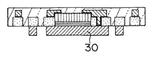
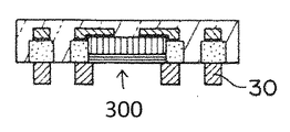
かかる第2実施形態の特徴は、第1金属層30において電子部品10の直下領域300が局所的に除去されており、電子部品10の下面からの発光を取り出すことができるように構成されていることである。かかる場合、接着剤層70は、光学特性に優れた材料から成っていてもよい。つまり、接着剤層70が光透過性を有していてもよい。これにより、電子部品10の下面からの発光をより好適に取り出すことができる。尚、かかる第2実施形態では、第1金属層30を反射板として設けてもよい。
The feature of the second embodiment is that the
上記の如くの第1実施形態および第2実施形態では、伸縮性フレキシブル基板100はマトリックス状に配置された単位配線構造110を備えているが、これは、複数の単位配線構造110が一定方向に沿って配置されているまたはそれに加えて当該一定方向と交差する方向にも配置されている態様といえる。また、図示される形態から分かるように、単位配線構造同士を接続する湾曲配線部は、変曲点を有するように湾曲していてもよい。
In the first embodiment and the second embodiment as described above, the stretchable
[本開示の伸縮性フレキシブル基板の製造方法]
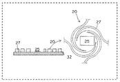
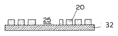
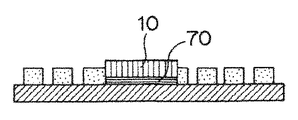
次に、本開示の一態様に係る伸縮性フレキシブル基板の製造方法について説明する。図11A〜11Hに本開示の製造方法に関連したプロセスを模式的に示している。本開示の製造方法は、まず工程(i)を実施する。即ち、図11Aおよび11Bに示すように第1金属層の前駆部材32上に第1絶縁層20を設ける。具体的には、第1金属層の前駆部材32上に「電子部品配置のための中空領域25を有すると共にその中空領域25を中心として湾曲するように延在する湾曲部27を有する第1絶縁層20」を設ける。
[Method of manufacturing stretchable flexible substrate of the present disclosure]
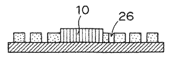
Next, a method for manufacturing a stretchable flexible substrate according to one embodiment of the present disclosure will be described. 11A to 11H schematically show processes related to the manufacturing method of the present disclosure. In the manufacturing method of the present disclosure, step (i) is first performed. That is, as shown in FIGS. 11A and 11B, the first insulating
かかる工程(i)の第1金属層の前駆部材32としては、金属箔を用いてもよい。かかる金属箔の厚さは、9μm〜1000μm程度であってもよく、18μm〜500μm程度であってもよく、20μm〜100μm程度であってもよい。金属箔は、例えば、銅(Cu)、ニッケル(Ni)およびアルミニウム(Al)から成る群から選択される少なくとも1種の金属材料を含んで成る。あくまでも例示にすぎないが、金属箔として銅箔を用いてもよい。
As the
金属層の前駆部材32としては「複数の層構成から構成された部材」を用いてもよい。例えば、後に剥離およびエッチング除去が可能な支持材付き金属箔を用いてよく、あるいは、表面にエッチングストップ層が形成された金属箔などを用いてもよい。
As the metal
前駆部材32上に設けられる第1絶縁層20は樹脂層であってよい。かかる場合、「金属層の前駆部材32上において電子部品配置のための中空領域25を有すると共にその中空領域25を中心として湾曲するように延在する湾曲部27を有する樹脂層」を設けることになる。かかる樹脂層の形成方法としては、液状原料の場合、スクリーン印刷、オフセット印刷、グラビア印刷、グラビアオフセット印刷、インクジェット印刷、反転印刷またはフレキソ印刷などの印刷法を用いてよい。また、樹脂層の原料として感光性を有する樹脂原料を使用してもよい。その場合、エッチング処理などを通じて、樹脂層に「電子部品配置のための中空領域25、およびその中空領域25を中心として湾曲するように延在する湾曲部27を有するようなパターン」をより好適に形成することができる。具体的には、前駆部材32の全面に感光性樹脂原料から成る層を形成し、次いで、その層をエッチング処理してパターニングすることによって、所望の樹脂層を得ることができる。パターニング処理自体は、エレクトロニクス実装分野で用いられている処理であれば特に制限はない。例えば、樹脂層形成、露光・現像、エッチングなどを実施するフォトリソグラフィーを利用することによって所望のパターニング処理を実施してよい。
The first insulating
工程(i)に引き続いて、工程(ii)を実施する。即ち、図11Cに示すように、“中空領域25”に電子部品10を配置する。つまり、前駆部材32上の第1絶縁層20によって形成された“凹部”の領域に対して電子部品10を配置する。配置される電子部品10は、例えば、半導体素子(発光素子、受光素子、ダイオードおよびトランジスタなどを含む)、温度センサ、圧力センサまたはアクチュエーター等の他、IC(例えばコントロールIC)、インダクタ、コンデンサ、パワー素子、チップ抵抗、チップコンデンサ、チップバリスタ、チップサーミスタ、その他チップ状の積層フィルター、または、接続端子などである。
Subsequent to step (i), step (ii) is performed. That is, as shown in FIG. 11C, the
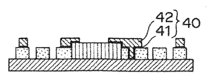
工程(ii)に引き続いて、工程(iii)を実施する。即ち、図11Dおよび図11Eに示すように、めっき処理を実施し、かかるめっき処理によって形成された金属めっき層44に対してパターニング処理を実施して第2金属層40を形成する。めっき処理では、前駆部材32、電子部品10および樹脂層20に対して全体的に金属めっき層44を形成する。また、図示する態様から分かるように、工程(iii)では、湾曲部27に起因してもたらされる第1絶縁層20の間隙部26を満たすように第2金属層40を形成し、それによって、その間隙部26の位置に「第1金属層30と第2金属層40とを互いに接続する層間接続部位」を最終的に形成してもよい。
Subsequent to step (ii), step (iii) is performed. That is, as shown in FIGS. 11D and 11E, a plating process is performed, and a patterning process is performed on the
かかる工程(iii)のめっき処理としては、乾式めっき法を実施した後で湿式めっき法を実施してもよい。つまり、乾式めっき法を実施して乾式めっき層41を形成した後、湿式めっき法を実施することによって湿式めっき層42を形成してもよい。これにより、乾式めっき層41と湿式めっき層42との2層構造から成る金属めっき層44を形成することができ、かかる金属めっき層44に対してパターニング処理を実施して当該2層構造から成る第2金属層40を形成できる。
As the plating treatment in the step (iii), the wet plating method may be performed after the dry plating method is performed. That is, the
乾式めっき法としては、真空めっき法(PVD法)または化学気相めっき法(CVD法)を実施してよい。真空めっき法(PVD法)にはスパッタリング、真空蒸着およびイオンプレーディングなどが含まれる。一方、湿式めっき法としては、電気めっき法(例えば電解めっき)、化学めっき法または溶融めっき法などを実施してよい。ある一態様として、本開示の製造方法では、乾式めっき法としてスパッタリングを実施し、湿式めっき法として電気めっき法(例えば電解めっき)を実施してもよい。 As the dry plating method, a vacuum plating method (PVD method) or a chemical vapor plating method (CVD method) may be performed. The vacuum plating method (PVD method) includes sputtering, vacuum deposition and ion plating. On the other hand, as the wet plating method, an electroplating method (for example, electrolytic plating), a chemical plating method, a hot dipping method, or the like may be performed. As one aspect, in the manufacturing method of the present disclosure, sputtering may be performed as a dry plating method, and an electroplating method (for example, electrolytic plating) may be performed as a wet plating method.
尚、乾式めっき法を実施した後で、湿式めっき法を実施することによって、「相対的に小さい平均結晶粒径から成る乾式めっき層41」および「相対的に大きい平均結晶粒径から成る湿式めっき層42」を形成できる。つまり、乾式めっき法で“相対的に小さい平均結晶粒径から成る下地層を形成し、その後、湿式めっき法で“相対的に大きい平均結晶粒径から成る肉厚の層を形成することができ、平均結晶粒径が互いに異なる2層構造の金属めっき層44を形成することができる。このように乾式めっき法と湿式めっき法とを利用する製造方法は、「前駆部材32、電子部品10および樹脂層に対してダイレクトに金属層を形成する」といったプロセス的特徴を有している。「肉厚の湿式めっき層42の下地層となる乾式めっき層41」は非常に薄く設けることができ、かかる肉厚の湿式めっき層42が前駆部材32、電子部品10および樹脂層に対してダイレクトに面接触していると捉えることができるからである。肉厚の湿式めっき層42に起因して金属めっき層44は厚く設けることができ、それゆえ、「湾曲部27に起因してもたらされる第1絶縁層20の間隙部26」を満たすように金属めっき層44を形成することができる。また、特に製造プロセスの点に着目してみると、乾式めっき法を実施するからこそ、後刻の湿式めっき法でめっき層を厚くかつ密着力良く形成できるといえる。
In addition, after carrying out the dry plating method, by carrying out the wet plating method, “the
乾式めっき法を実施して100nm〜3000nm厚さの乾式めっき層41を形成し、次いで、湿式めっき法を実施して18μm〜500μm厚さの湿式めっき層42を形成してもよい(図11D参照)。乾式めっき法によって形成される乾式めっき層41は、例えば、Ti(チタン)、Cr(クロム)およびNi(ニッケル)から成る群から選択される少なくとも1種類の金属材料を含んでいてもよい。一方、湿式めっき法によって形成される湿式めっき層42は、Cu(銅)、Ni(ニッケル)およびAl(アルミニウム)から成る群から選択される少なくとも1種類の金属材料を含んでいてもよい。尚、あくまでも一例にすぎないが、乾式めっき層41は、単一層として形成することに限らず、複数の層として形成してもよい。例えば、乾式めっき層41として、スパッタリングによりTi薄膜層とCu薄膜層とを形成してよい。より具体的には、Ti薄膜層を形成した後にCu薄膜層を形成してよい。この場合、かかる2層構造のスパッタ層上に湿式めっき層42として厚いCuめっき層を電解めっきにより形成してもよい。
A dry plating method may be performed to form a
金属めっき層44はパターニング処理に付され、それによって、最終的に金属めっき層44から第2金属層40が得られる(図11E参照)。かかるパターニング処理自体は、エレクトロニクス実装分野で用いられている処理であれば特に制限はない。例えば、レジスト形成、露光・現像、エッチングなどを実施するフォトリソグラフィーを利用することによって所望のパターニング処理を実施してよい。
The
工程(iii)に引き続いて、工程(iv)を実施する。即ち、図11Fに示すように、電子部品10、第1絶縁層20および第2金属層40を封止するように前駆部材32上に第2絶縁層50を形成する。第2絶縁層50としては、樹脂層を形成してよい。つまり、金属めっき層44のパターニング面側を封止樹脂層で被覆してよい。
Subsequent to step (iii), step (iv) is performed. That is, as shown in FIG. 11F, the second insulating
かかる第2絶縁層50の形成は、後刻の工程において単位配線構造の湾曲配線部が“中空構造”になることを防ぐことができる点でも有利である。
The formation of the second insulating
本開示の製造方法では、第1絶縁層20および第2絶縁層50をそれぞれ樹脂層として形成してもよく、第2絶縁層50を第1絶縁層20よりも軟質の樹脂材から形成してもよい。つまり、第1絶縁層20を、アクリル樹脂、ウレタン樹脂、シリコーン樹脂、フッ素樹脂、ポリイミド樹脂およびエポキシ樹脂から成る群から選択される少なくとも1種以上の樹脂材料を含んで成る樹脂層として形成する場合、第2絶縁層50をエラストマー材を含んで成る樹脂層として形成してもよい。
In the manufacturing method of the present disclosure, each of the first insulating
つまり、封止樹脂層に用いる封止樹脂原料はエラストマーなどの可撓性を有する原料であってもよい。例えば液状の封止樹脂原料の場合であれば、塗布を通じて封止樹脂層を形成してよい。かかる塗布の具体的手法は、特に制限されず、例えばスピンコート法、ロールコート法、カーテンコート法、スプレー法または液滴吐出法等を用いてよい。また、封止樹脂材を予めシート化したものを加熱圧着により前駆部材32上に設けることによって封止樹脂層を形成してもよい。
That is, the sealing resin raw material used for the sealing resin layer may be a flexible raw material such as an elastomer. For example, in the case of a liquid sealing resin raw material, the sealing resin layer may be formed through coating. The specific method of the application is not particularly limited, and for example, a spin coat method, a roll coat method, a curtain coat method, a spray method, a droplet discharge method, or the like may be used. Alternatively, the sealing resin layer may be formed by providing a sheet of the sealing resin material in advance on the
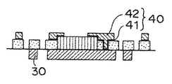
工程(iv)に引き続いて、工程(v)を実施する。即ち、図11Fおよび11Gに示すように、前駆部材32をパターニング処理することによって、かかる前駆部材32から第1金属層30を得る。かかるパターニング処理自体も、エレクトロニクス実装分野で用いられている処理であれば特に制限はない。例えば、レジスト形成、露光・現像、エッチングなどを実施するフォトリソグラフィーを利用することによって所望のパターニング処理を実施してよい。
Subsequent to step (iv), step (v) is performed. That is, as shown in FIGS. 11F and 11G, the
以上の工程を経ることによって、最終的に上述した如くの本開示の伸縮性フレキシブル基板100を得ることができる。つまり、電子部品10の周囲に位置付けられた第1絶縁層20の両面にそれぞれ接するように第1金属層30と第2金属層40とが設けられると共に、かかる第1絶縁層20、電子部品10および第2金属層40を封止する第2絶縁層50が設けられた伸縮性フレキシブル基板100を得ることができる。
Through the above steps, the stretchable
尚、図11Hに示すように、工程(v)の後、第1金属層30を封止するように第3絶縁層60を形成してもよい。特に、第2絶縁層50に対して積層された形態となるように第3絶縁層60を形成してもよい。これにより、互いに積層された第2絶縁層50と第3絶縁層60の内部にて電子部品10、第1絶縁層20、第1金属層30、第2金属層40が埋設された形態が得られる。
In addition, as shown to FIG. 11H, you may form the 3rd insulating
本開示の製造方法では、第1絶縁層20および第3絶縁層60をそれぞれ樹脂層として形成してもよく、第3絶縁層60を第1絶縁層20よりも軟質の樹脂材から形成してもよい。つまり、第1絶縁層20が、アクリル樹脂、ウレタン樹脂、シリコーン樹脂、フッ素樹脂、ポリイミド樹脂およびエポキシ樹脂から成る群から選択される少なくとも1種以上の樹脂材料を含んで成る樹脂層として形成する場合、第3絶縁層60をエラストマー材を含んで成る樹脂層として形成してもよい。
In the manufacturing method of the present disclosure, the first insulating
つまり、第2絶縁層50と同様、第3絶縁層60である封止樹脂層に用いる封止樹脂原料はエラストマーなどの可撓性を有する原料であってもよい。例えば液状の封止樹脂原料の場合であれば、塗布を通じて封止樹脂層を形成してよい。かかる塗布の具体的手法は、特に制限されず、例えばスピンコート法、ロールコート法、カーテンコート法、スプレー法または液滴吐出法等を採用してよい。また、封止樹脂材を予めシート化したものを加熱圧着により設けることによって封止樹脂層を形成してもよい。
That is, like the second insulating
本開示の製造方法は、種々の態様で実施することができる。上記の図11A〜11Hに示す態様では、第2絶縁層50の形成後に前駆部材32をパターニング処理して第1金属層30を得る態様であったが、それらを逆にしてもよい。つまり、前駆部材32をパターニング処理して第1金属層30を形成した後に第2絶縁層50を形成してもよい。これは、工程(iv)に先立って、工程(v)を実施することを意味している。かかる態様に係る製造プロセスを図12A〜12Hに示す。
The manufacturing method of the present disclosure can be implemented in various modes. 11A to 11H described above, the
図12A〜12Hに示される製造方法では、上記工程(i)、(ii)および(iii)の後に、
(a)前駆部材32をパターニング処理して第1金属層30を得る工程、
(b)電子部品10、第1絶縁層20および第2金属層40を封止するように前駆部材上に第2絶縁層50を形成する工程
が実施される。
In the manufacturing method shown in FIGS. 12A to 12H, after the steps (i), (ii) and (iii),
(A) A step of patterning the
(B) The process of forming the 2nd insulating
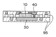
これによっても伸縮性フレキシブル基板100を得ることができる(図12Gまたは12H参照)。つまり、電子部品10の周囲に位置付けられた第1絶縁層20の両面にそれぞれ接するように第1金属層30と第2金属層40とが設けられると共に、かかる第1絶縁層20、電子部品10および第2金属層40を封止する第2絶縁層50が設けられた伸縮性フレキシブル基板100を得ることができる。尚、かかる態様では、第2絶縁層50の形成を第3絶縁層60の形成と同時に行ってよい。つまり、図12Fおよび12Iに示すように、第1絶縁層20、電子部品10および第2金属層40のみならず、第1金属層30をも一体的に封止する絶縁層95(例えば封止樹脂層)を一括で形成してもよい。更にいえば、図12A〜12Hに示される態様では、「第2金属層40を得るためのパターニング処理」と「第1金属層30を得るためのパターニング処理」とを実質的に同時に実施してもよい。つまり、金属めっき層44および前駆部材32に対してパターニング処理を実施して第2金属層40および第1金属層30を一括して形成してもよい。これは、工程(iv)に先立って工程(v)を実施するに際して、「工程(iii)の第1パターニング処理」と「工程(v)の第2パターニング処理」とを一括または同時に行うことを意味している。
This also makes it possible to obtain the stretchable flexible substrate 100 (see FIG. 12G or 12H). That is, the
(第1実施形態の伸縮性フレキシブル基板の製造方法)
図13A〜13Iは、上記第1実施形態の伸縮性フレキシブル基板100を得るための製造プロセスが模式的に示されている。
(Method for manufacturing the stretchable flexible substrate of the first embodiment)
13A to 13I schematically show a manufacturing process for obtaining the stretchable
図示する対応から分かるように、第1実施形態の伸縮性フレキシブル基板100を得る製造プロセスは、上述の図11A〜11Hに示す製造プロセスと同様であり、相違点は接着剤層70の形成に存する。
As can be seen from the illustrated correspondence, the manufacturing process for obtaining the stretchable
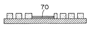
具体的には、工程(ii)において、“中空領域25”に接着剤層70を形成した後、かかる接着剤層70と接するように電子部品10を配置する(図13B〜13D参照)。つまり、前駆部材32上の第1絶縁層20によって形成された“凹部”の領域に接着剤層70を形成した後で電子部品10を配置する。接着剤層70の形成自体は、塗布法を通じて行ってよい。かかる塗布法としては、上述した各種印刷方法およびディスペンサーなどによる塗布法を挙げることができる。
Specifically, in step (ii), after the
このような接着剤層70の形成工程が付加されていること以外は、上述の図11A〜11Hに示す製造プロセスと同様であるので、重複を避けるべく詳細な説明は省略する。
Since the manufacturing process shown in FIGS. 11A to 11H is the same as the manufacturing process shown in FIGS. 11A to 11H except that the formation process of the
(第2実施形態の伸縮性フレキシブル基板の製造方法)
図14A〜14Iは、上記第2実施形態の伸縮性フレキシブル基板100を得るための製造プロセスが模式的に示されている。図示する対応から分かるように、第2実施形態の伸縮性フレキシブル基板100を得る製造プロセスも、上述の図11A〜11Hに示す製造プロセスと同様である。相違点は接着剤層70の形成に加えて、前駆部材32のパターニング処理の相違に存する。
(Method for producing stretchable flexible substrate of second embodiment)
14A to 14I schematically show a manufacturing process for obtaining the stretchable
特に、第2実施形態の伸縮性フレキシブル基板100の製造方法では前駆部材32のパターニング処理に際して、電子部品10の直下領域の前駆部材32を除去する。具体的には、図14Gおよび14Hに示すように、前駆部材32のパターニング処理で、電子部品の直下領域300を除去して第1金属層30を得る。これにより、電子部品10の下面からの発光を取り出すことができるようになる。
In particular, in the method of manufacturing the stretchable
尚、接着剤層70の形成については、上述の図13B)〜13Dの場合と同じである。但し、接着剤層70としては、光学特性に優れた材料から接着剤層70を形成してもよい。電子部品10の下面からの発光をより好適に取り出すことができるからである。
In addition, about formation of the
このような前駆部材32のパターニング処理および接着剤層70の形成以外は、上述の図11A〜11Hに示す製造プロセスと同様であるので、重複を避けるべく詳細な説明は省略する。
Except for the patterning process of the
[本開示の基板の伸縮性/単位配線構造について]
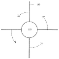
最後に、本願発明者が本開示に係る伸縮性フレキシブル基板を案出するに至る前段階での思想について付言しておく。本願発明者は、従来のフレキシブル基板が有する問題、すなわち応力が一部に集中して破断しやすくなるという問題を解決するために、これまでの「屈曲した」配線部に代えて、応力が分散されるように「湾曲した」配線部を用いることを案出した。すなわち、本願発明者は、図15に示すように、中心部120の周りに例えば反時計周り方向(又は時計周り方向)に回転させることで湾曲する配線部180を用いることにより、応力を一箇所に集中させることなく分散できると考えた。かかる思想に基づき、本開示の伸縮性フレキシブル基板を案出するに至った。
[About the elasticity / unit wiring structure of the substrate of the present disclosure]
Finally, the idea at the stage before the inventor devised the stretchable flexible substrate according to the present disclosure will be added. In order to solve the problem that the conventional flexible substrate has, that is, the problem that the stress is concentrated on a part and easily breaks, the inventor of the present application distributes the stress instead of the conventional “bent” wiring part. It was devised to use a “curved” wiring section as described. That is, as shown in FIG. 15, the inventor of the present application uses a
本開示の一態様に係る伸縮性フレキシブル基板は、1又は2以上の単位配線構造を有し、その単位配線構造は、中心部と、その中心部の外側に設けられた湾曲配線部を有して成る。湾曲配線部は、一端が同じ単位配線構造に属する中心部の外周に接続されて外周に沿って延在するように設けられており、他端が、例えば、隣接する単位配線構造の湾曲配線部に接続されている。本実施形態において、湾曲配線部は、少なくとも湾曲した配線部を有していればよい。例えば、図1および図5等に示される伸縮性フレキシブル基板100では、中心部120に電子部品10を実装されている。かかる電子部品10は電極パターン140を介して湾曲配線部160と電気的に接続されている。湾曲配線部160は、中心部120の外周に沿って約180度湾曲した形態を有している。本開示では、中心部120の中心を基点として、湾曲配線部160が中心部の外周に沿って湾曲して設けられている部分の角度を湾曲中心角と捉えることができる。かかる湾曲中心角には種々のものが考えられる。例えば、湾曲配線部160は、中心部120の外周に沿って約30度湾曲して設けられていてもよく、あるいは、中心部120の外周に沿って約90度湾曲して設けられていてもよい。隣接する単位配線構造の配置パターンを増やすべく、湾曲配線部160が、中心部120の外周に沿って約60度以上湾曲していてもよい。更にいえば、湾曲配線部160が、中心部120の外周に沿って約360度以上湾曲して設けられていてもよい。湾曲配線部160が、中心部120の外周に沿って約360度以上湾曲している場合、湾曲配線部は中心部の外周に沿ってより明確に巻回したような形態を有し得る。かかる場合、湾曲配線部160が、中心部120の外周に沿って1〜3周程巻回する形態となっていてもよい。なお、中心部120の形状は特に限定されるものではない。つまり、中心部120の形状は、図示されたような円形に特に限定されるものでなく、それ以外に四角形および六角形等の多角形の形状を採ることができる。中心部120の形状が多角形の場合、その頂点が湾曲配線部160の湾曲に合わせてR面取りされていてもよい。
The stretchable flexible substrate according to one embodiment of the present disclosure has one or more unit wiring structures, and the unit wiring structure includes a central portion and a curved wiring portion provided outside the central portion. It consists of The curved wiring portion is provided so that one end is connected to the outer periphery of the central portion belonging to the same unit wiring structure and extends along the outer periphery, and the other end is, for example, the curved wiring portion of the adjacent unit wiring structure It is connected to the. In the present embodiment, the curved wiring portion only needs to have at least a curved wiring portion. For example, in the stretchable
伸縮性フレキシブル基板100の伸張に伴い、中心部120の外周に沿って設けられた湾曲配線部160の曲率は、伸縮前と比べて小さくなるように変化する。ここでいう「曲率」とは、湾曲配線部の湾曲形状の曲率(即ち「湾曲配線部の湾曲程度/曲がり具合」)を指しており、かかる曲率は湾曲配線部の曲率半径の逆数を指す。典型的な態様に従えば、湾曲配線部160は一端から湾曲配線部160の他端に向かうにつれて、中心部120の外周から離れるように変形して曲率が小さくなり、伸張に供する。本開示の伸縮性フレキシブル基板100は、中心部120の外周に沿って設けられた湾曲配線部160の曲率を変化させて伸縮させているので、湾曲配線部全体が変形して伸縮することになり、応力を湾曲配線部全体に分散させることができる。従って、本開示の伸縮性フレキシブル基板100は、応力の集中が生じにくく、破断の発生が抑制されているといえる。
Along with the expansion of the stretchable
また、本実施形態の伸縮性フレキシブル基板では、中心部120に沿って湾曲させる中心角を大きくしたり、捲回の回数を増やしたりすることで湾曲配線部160の長さを大きくすることが可能であることから、より大きな伸縮性を持たせることができる。つまり、伸縮前の初期状態の基板寸法を小さくすることも可能である。
Further, in the stretchable flexible substrate of the present embodiment, the length of the
以上、本開示の伸縮性フレキシブル基板について説明してきたが、本開示はこれに限定されることなく、特許請求の範囲に規定される開示の範囲から逸脱することなく種々の変更が当業者によってなされると理解されよう。 Although the stretchable flexible substrate of the present disclosure has been described above, the present disclosure is not limited thereto, and various modifications can be made by those skilled in the art without departing from the scope of the disclosure defined in the claims. Will be understood.
例えば、本開示の伸縮性フレキシブル基板の製造方法の第2絶縁層および/または第3絶縁層の形成は、最終的な伸縮性フレキシブル基板にとって必要な部分、例えば、電子部品または湾曲配線部のみに形成してもよい。 For example, the second insulating layer and / or the third insulating layer in the manufacturing method of the elastic flexible substrate of the present disclosure is formed only on a part necessary for the final elastic flexible substrate, for example, an electronic component or a curved wiring portion. It may be formed.
本開示の一態様に係る伸縮性フレキシブル基板は、エレクトロニクス機器の分野の範疇に留まらず、ウェアラブル機器の分野、ヘルスケア分野、医療分野および介護分野などにおいても利用可能である。例えば、ウェアラブル機器など人体などの動きに追随した伸縮や柔軟な変形が求められる電子デバイスにおいて、本開示の一態様に係る伸縮性フレキシブル基板を高い伸縮性、信頼性を呈する基板として好適に用いることができる。 The stretchable flexible substrate according to one embodiment of the present disclosure is not limited to the category of the field of electronics equipment, but can be used in the field of wearable equipment, the health care field, the medical field, and the nursing field. For example, in an electronic device that requires expansion and contraction and flexible deformation following movement of a human body such as a wearable device, the elastic flexible substrate according to one embodiment of the present disclosure is preferably used as a substrate exhibiting high elasticity and reliability. Can do.
10 電子部品
20 第1絶縁層
20A 第1絶縁層の一部
20B 第1絶縁層の他部
25 中空領域
26 間隙部
27 湾曲部
30 第1金属層
30A 第1金属層の一部
30B 第1金属層の他部
32 第1金属層の前駆部材
40 第2金属層
40A 第2金属層の一部
40B 第2金属層の他部
41 乾式めっき層
42 湿式めっき層
44 金属めっき層
50 第2絶縁層
60 第3絶縁層
70 接着剤層
80 層間接続部位
90 凹部
95 絶縁層
100 伸縮性フレキシブル基板
110 単位配線構造
120 中心部
140 電極パターン
160 湾曲配線部
202 第1絶縁層の第1主面
204 第1絶縁層の第2主面
300 電子部品の直下領域
DESCRIPTION OF
Claims (23)
前記電子部品の周囲に位置付けられ、互いに対向する第1主面および第2主面を有する第1絶縁層、
前記第1主面と接する第1金属層、
前記第2主面と接し、前記電子部品と電気的に接続された第2金属層、ならびに
前記電子部品、前記第1絶縁層および前記第2金属層を封止する第2絶縁層
を備え、
平面視において、
少なくとも前記電子部品と、前記第1絶縁層の一部と、前記第1金属層の一部と、前記第2金属層の一部とから構成される中心部から、
少なくとも前記第1絶縁層の前記一部以外の他部と、前記第1金属層の前記一部以外の他部と、前記第2金属層の前記一部以外の他部とから構成される少なくとも1つの湾曲配線部が延びており、
前記少なくとも1つの湾曲配線部は、少なくとも部分的に湾曲している、伸縮性フレキシブル基板。 Electronic components,
A first insulating layer positioned around the electronic component and having a first main surface and a second main surface facing each other;
A first metal layer in contact with the first main surface;
A second metal layer in contact with the second main surface and electrically connected to the electronic component; and a second insulating layer for sealing the electronic component, the first insulating layer and the second metal layer,
In plan view,
From a central portion constituted by at least the electronic component, a part of the first insulating layer, a part of the first metal layer, and a part of the second metal layer,
At least other parts other than the part of the first insulating layer, other parts other than the part of the first metal layer, and other parts other than the part of the second metal layer. One curved wiring part extends,
The stretchable flexible substrate, wherein the at least one curved wiring portion is at least partially curved.
前記第2絶縁層が前記第1絶縁層よりも軟質である、請求項1から5のいずれかに記載の伸縮性フレキシブル基板。 The first insulating layer and the second insulating layer are both resin layers,
The stretchable flexible substrate according to any one of claims 1 to 5, wherein the second insulating layer is softer than the first insulating layer.
前記第2絶縁層と前記第3絶縁層とが互いに積層されている、請求項1から6のいずれかに記載の伸縮性フレキシブル基板。 A third insulating layer for sealing the first metal layer;
The stretchable flexible substrate according to any one of claims 1 to 6, wherein the second insulating layer and the third insulating layer are laminated with each other.
前記第2絶縁層と前記第3絶縁層とが互いに積層されており、
前記接着剤層が、前記第2絶縁層と前記第3絶縁層との界面に対して面一である、請求項4に記載の伸縮性フレキシブル基板。 A third insulating layer for sealing the first metal layer;
The second insulating layer and the third insulating layer are stacked on each other;
The stretchable flexible substrate according to claim 4, wherein the adhesive layer is flush with an interface between the second insulating layer and the third insulating layer.
前記第3絶縁層が前記第1絶縁層よりも軟質である、請求項7から10のいずれかに記載の伸縮性フレキシブル基板。 The first insulating layer and the third insulating layer are both resin layers,
The stretchable flexible substrate according to any one of claims 7 to 10, wherein the third insulating layer is softer than the first insulating layer.
前記間隙を通して、前記第1金属層と前記第2金属層とを電気的に接続されている、請求項1から11のいずれかに記載の伸縮性フレキシブル基板。 A gap penetrating the first insulating layer;
The stretchable flexible substrate according to any one of claims 1 to 11, wherein the first metal layer and the second metal layer are electrically connected through the gap.
(ii)前記中空領域に電子部品を配置する工程、
(iii)めっき処理を実施し、前記めっき処理によって形成されためっき層に対して第1パターニング処理を実施して第2金属層を形成する工程、
(iv)前記電子部品、前記第1絶縁層および前記第2金属層を封止するように前記前駆部材上に第2絶縁層を形成する工程、および
(v)前記前駆部材を第2パターニング処理して第1金属層を得る工程
を含む、伸縮性フレキシブル基板の製造方法。 (I) providing a first insulating layer having a hollow region and at least one curved portion extending around the hollow region on the precursor member of the first metal layer;
(Ii) a step of arranging an electronic component in the hollow region;
(Iii) performing a plating process and performing a first patterning process on the plating layer formed by the plating process to form a second metal layer;
(Iv) forming a second insulating layer on the precursor member so as to seal the electronic component, the first insulating layer, and the second metal layer; and (v) performing a second patterning process on the precursor member. And the manufacturing method of a stretchable flexible substrate including the process of obtaining a 1st metal layer.
前記第2絶縁層を前記第1絶縁層よりも軟質の樹脂材を用いて形成する、請求項14または15に記載の伸縮性フレキシブル基板の製造方法。 Forming each of the first insulating layer and the second insulating layer as a resin layer;
The method for producing a stretchable flexible substrate according to claim 14 or 15, wherein the second insulating layer is formed using a resin material softer than the first insulating layer.
前記第3絶縁層を前記第1絶縁層よりも軟質の樹脂材を用いて形成する、請求項17に記載の伸縮性フレキシブル基板の製造方法。 Forming each of the first insulating layer and the third insulating layer as a resin layer;
The method for manufacturing a stretchable flexible substrate according to claim 17, wherein the third insulating layer is formed using a resin material softer than the first insulating layer.
Applications Claiming Priority (2)
| Application Number | Priority Date | Filing Date | Title |
|---|---|---|---|
| JP2015105757 | 2015-05-25 | ||
| JP2015105757 | 2015-05-25 |
Publications (2)
| Publication Number | Publication Date |
|---|---|
| JP2016219782A true JP2016219782A (en) | 2016-12-22 |
| JP6712764B2 JP6712764B2 (en) | 2020-06-24 |
Family
ID=57399559
Family Applications (1)
| Application Number | Title | Priority Date | Filing Date |
|---|---|---|---|
| JP2016058851A Active JP6712764B2 (en) | 2015-05-25 | 2016-03-23 | Stretchable flexible substrate and manufacturing method thereof |
Country Status (3)
| Country | Link |
|---|---|
| US (1) | US9860979B2 (en) |
| JP (1) | JP6712764B2 (en) |
| CN (1) | CN106211545A (en) |
Cited By (10)
| Publication number | Priority date | Publication date | Assignee | Title |
|---|---|---|---|---|
| WO2018174164A1 (en) * | 2017-03-23 | 2018-09-27 | パナソニックIpマネジメント株式会社 | Tactile sensor, and tactile sensor unit constituting said tactile sensor |
| WO2018199084A1 (en) * | 2017-04-28 | 2018-11-01 | 株式会社村田製作所 | Wiring substrate and method for manufacturing same |
| WO2019088099A1 (en) * | 2017-10-31 | 2019-05-09 | ダイキン工業株式会社 | Member for wearable terminal |
| WO2019088098A1 (en) * | 2017-10-31 | 2019-05-09 | ダイキン工業株式会社 | Layered product |
| JP2019537276A (en) * | 2016-09-27 | 2019-12-19 | ティーティーワイ−サーティオ エスアール | Stretchable structure including conductive path and method of manufacturing the structure |
| KR20200021873A (en) | 2018-08-21 | 2020-03-02 | 엘지디스플레이 주식회사 | Electronic Component And Display Device |
| WO2020066121A1 (en) * | 2018-09-26 | 2020-04-02 | 住友理工株式会社 | Capacitance sensor, method for manufacturing same, and reticulated soft electrode for capacitance sensor |
| WO2020137148A1 (en) * | 2018-12-26 | 2020-07-02 | ソニー株式会社 | Flexible wiring board and electronic device |
| JPWO2020213681A1 (en) * | 2019-04-18 | 2020-10-22 | ||
| KR20210001912A (en) | 2019-06-28 | 2021-01-06 | 엘지디스플레이 주식회사 | Connector installed on stretchable substrate and stretchable display device |
Families Citing this family (4)
| Publication number | Priority date | Publication date | Assignee | Title |
|---|---|---|---|---|
| US10080290B2 (en) * | 2015-11-17 | 2018-09-18 | Intel Corporation | Stretchable embedded electronic package |
| JP7065463B2 (en) * | 2017-07-12 | 2022-05-12 | パナソニックIpマネジメント株式会社 | Metal-clad laminate, metal leaf with resin, and wiring board |
| USD948497S1 (en) | 2019-09-23 | 2022-04-12 | Hip Innovations, Llc | Combined stand and extendable member for mobile devices |
| US20250016931A1 (en) * | 2021-07-30 | 2025-01-09 | Liquid Wire Inc. | Flexible and stretchable structures |
Citations (5)
| Publication number | Priority date | Publication date | Assignee | Title |
|---|---|---|---|---|
| JP2003152286A (en) * | 2001-11-12 | 2003-05-23 | Yazaki Corp | Silent structure of mounting board |
| JP2010226069A (en) * | 2009-03-19 | 2010-10-07 | Samsung Electro-Mechanics Co Ltd | Electronic component built-in printed circuit board |
| WO2011016555A1 (en) * | 2009-08-07 | 2011-02-10 | 日本電気株式会社 | Semiconductor device and method for manufacturing same |
| JP2012204831A (en) * | 2011-03-23 | 2012-10-22 | Ibiden Co Ltd | Electronic component built-in wiring board and manufacturing method of the same |
| JP2016520986A (en) * | 2013-02-06 | 2016-07-14 | ザ ボード オブ トラスティーズ オブ ザ ユニヴァーシティー オブ イリノイ | Self-similar fractal design for stretchable electronics |
Family Cites Families (17)
| Publication number | Priority date | Publication date | Assignee | Title |
|---|---|---|---|---|
| DE10235311B4 (en) | 2002-08-01 | 2006-09-28 | Yazaki Europe Ltd., Hemel Hempstead | Flexible conductor element |
| JP2004349002A (en) | 2003-05-20 | 2004-12-09 | Hitachi Chem Co Ltd | Wiring member for transport aircraft and its manufacturing method |
| JP2008010368A (en) | 2006-06-30 | 2008-01-17 | Advanced Telecommunication Research Institute International | WIRING, MANUFACTURING METHOD THEREOF, AND CIRCUIT DEVICE |
| JP5285385B2 (en) | 2008-10-15 | 2013-09-11 | 株式会社フジクラ | Manufacturing method of multilayer wiring board |
| WO2010086033A1 (en) * | 2009-01-30 | 2010-08-05 | Interuniversitair Microelektronica Centrum Vzw | Stretchable electronic device |
| WO2010086034A1 (en) * | 2009-01-30 | 2010-08-05 | Interuniversitair Microelektronica Centrum Vzw | Stretchable electronic device |
| US8332053B1 (en) * | 2009-04-28 | 2012-12-11 | Hrl Laboratories, Llc | Method for fabrication of a stretchable electronic skin |
| JP5505415B2 (en) | 2009-07-16 | 2014-05-28 | 日本電気株式会社 | Wiring structure, cable, and manufacturing method of wiring structure |
| JP5823879B2 (en) | 2012-01-16 | 2015-11-25 | 日本メクトロン株式会社 | Flexible circuit board |
| EP2640168A1 (en) * | 2012-03-15 | 2013-09-18 | Nederlandse Organisatie voor toegepast-natuurwetenschappelijk Onderzoek TNO | Submount, assembly including submount, method of assembling and assembling device |
| JP2013195331A (en) | 2012-03-22 | 2013-09-30 | Jsr Corp | Anisotropic conductive sheet and its application |
| JP6009228B2 (en) | 2012-05-30 | 2016-10-19 | 新光電気工業株式会社 | Manufacturing method of electronic component built-in substrate |
| KR20140049314A (en) * | 2012-10-17 | 2014-04-25 | 한국전자통신연구원 | Stretchable electric device and manufacturing method of the same |
| JP2014162125A (en) | 2013-02-26 | 2014-09-08 | Fujikura Ltd | Stretchable circuit board, production method therefor, and electronic component including stretchable circuit board |
| JP6323982B2 (en) | 2013-02-26 | 2018-05-16 | 株式会社フジクラ | Electronic component having stretchable substrate and method for manufacturing the same |
| US20140299362A1 (en) * | 2013-04-04 | 2014-10-09 | Electronics And Telecommunications Research Institute | Stretchable electric device and manufacturing method thereof |
| KR20150069079A (en) * | 2013-12-12 | 2015-06-23 | 한국전자통신연구원 | stretchable device and manufacturing method of the same |
-
2016
- 2016-03-23 JP JP2016058851A patent/JP6712764B2/en active Active
- 2016-04-13 CN CN201610227456.0A patent/CN106211545A/en active Pending
- 2016-05-19 US US15/158,591 patent/US9860979B2/en active Active
Patent Citations (5)
| Publication number | Priority date | Publication date | Assignee | Title |
|---|---|---|---|---|
| JP2003152286A (en) * | 2001-11-12 | 2003-05-23 | Yazaki Corp | Silent structure of mounting board |
| JP2010226069A (en) * | 2009-03-19 | 2010-10-07 | Samsung Electro-Mechanics Co Ltd | Electronic component built-in printed circuit board |
| WO2011016555A1 (en) * | 2009-08-07 | 2011-02-10 | 日本電気株式会社 | Semiconductor device and method for manufacturing same |
| JP2012204831A (en) * | 2011-03-23 | 2012-10-22 | Ibiden Co Ltd | Electronic component built-in wiring board and manufacturing method of the same |
| JP2016520986A (en) * | 2013-02-06 | 2016-07-14 | ザ ボード オブ トラスティーズ オブ ザ ユニヴァーシティー オブ イリノイ | Self-similar fractal design for stretchable electronics |
Cited By (22)
| Publication number | Priority date | Publication date | Assignee | Title |
|---|---|---|---|---|
| JP2019537276A (en) * | 2016-09-27 | 2019-12-19 | ティーティーワイ−サーティオ エスアール | Stretchable structure including conductive path and method of manufacturing the structure |
| JPWO2018174164A1 (en) * | 2017-03-23 | 2020-01-23 | パナソニックIpマネジメント株式会社 | Tactile sensor and tactile sensor unit constituting the tactile sensor |
| WO2018174164A1 (en) * | 2017-03-23 | 2018-09-27 | パナソニックIpマネジメント株式会社 | Tactile sensor, and tactile sensor unit constituting said tactile sensor |
| US11137297B2 (en) | 2017-03-23 | 2021-10-05 | Panasonic Intellectual Property Management Co., Ltd. | Tactile sensor, and tactile sensor unit constituting tactile sensor |
| WO2018199084A1 (en) * | 2017-04-28 | 2018-11-01 | 株式会社村田製作所 | Wiring substrate and method for manufacturing same |
| KR20200061377A (en) * | 2017-10-31 | 2020-06-02 | 다이킨 고교 가부시키가이샤 | Absence for wearable terminals |
| JPWO2019088099A1 (en) * | 2017-10-31 | 2020-04-02 | ダイキン工業株式会社 | Material for wearable terminal |
| US11970611B2 (en) | 2017-10-31 | 2024-04-30 | Daikin Industries, Ltd. | Member for wearable device |
| WO2019088098A1 (en) * | 2017-10-31 | 2019-05-09 | ダイキン工業株式会社 | Layered product |
| WO2019088099A1 (en) * | 2017-10-31 | 2019-05-09 | ダイキン工業株式会社 | Member for wearable terminal |
| KR102365862B1 (en) * | 2017-10-31 | 2022-02-23 | 다이킨 고교 가부시키가이샤 | Member for wearable devices |
| JPWO2019088098A1 (en) * | 2017-10-31 | 2020-07-16 | ダイキン工業株式会社 | Laminate |
| KR20200021873A (en) | 2018-08-21 | 2020-03-02 | 엘지디스플레이 주식회사 | Electronic Component And Display Device |
| JP6714788B1 (en) * | 2018-09-26 | 2020-06-24 | 住友理工株式会社 | Capacitance sensor, manufacturing method thereof, and mesh-like flexible electrode for capacitance sensor |
| US11912331B2 (en) | 2018-09-26 | 2024-02-27 | Sumitomo Riko Company Limited | Capacitance sensor, method for manufacturing same, and reticulated soft electrode for capacitance sensor |
| WO2020066121A1 (en) * | 2018-09-26 | 2020-04-02 | 住友理工株式会社 | Capacitance sensor, method for manufacturing same, and reticulated soft electrode for capacitance sensor |
| WO2020137148A1 (en) * | 2018-12-26 | 2020-07-02 | ソニー株式会社 | Flexible wiring board and electronic device |
| WO2020213681A1 (en) * | 2019-04-18 | 2020-10-22 | パナソニックIpマネジメント株式会社 | Stretchable laminate, material for stretchable device, and stretchable device |
| JPWO2020213681A1 (en) * | 2019-04-18 | 2020-10-22 | ||
| US11864310B2 (en) | 2019-04-18 | 2024-01-02 | Panasonic Intellectual Property Management Co., Ltd. | Stretchable laminate, material for stretchable device, and stretchable device |
| JP7555053B2 (en) | 2019-04-18 | 2024-09-24 | パナソニックIpマネジメント株式会社 | Stretchable Devices |
| KR20210001912A (en) | 2019-06-28 | 2021-01-06 | 엘지디스플레이 주식회사 | Connector installed on stretchable substrate and stretchable display device |
Also Published As
| Publication number | Publication date |
|---|---|
| US9860979B2 (en) | 2018-01-02 |
| JP6712764B2 (en) | 2020-06-24 |
| CN106211545A (en) | 2016-12-07 |
| US20160353567A1 (en) | 2016-12-01 |
Similar Documents
| Publication | Publication Date | Title |
|---|---|---|
| JP6712764B2 (en) | Stretchable flexible substrate and manufacturing method thereof | |
| JP6667118B2 (en) | Flexible board | |
| JP6300156B2 (en) | Stretchable flexible substrate and manufacturing method thereof | |
| WO2020137148A1 (en) | Flexible wiring board and electronic device | |
| JPWO2018174164A1 (en) | Tactile sensor and tactile sensor unit constituting the tactile sensor | |
| US20080257586A1 (en) | Flexible circuit structure with stretchability and method of manufacturing the same | |
| JP2015198103A (en) | Stretchable flexible substrate and manufacturing method thereof | |
| CN108279800A (en) | The method and display device of scalable touch screen, the scalable touch screen of manufacture | |
| JP7119406B2 (en) | Stretchable wiring board and manufacturing method thereof | |
| JP6590391B1 (en) | Telescopic wiring member | |
| JP2018107208A (en) | Flexibility wiring board | |
| JP4799902B2 (en) | Wiring circuit board and method for manufacturing wiring circuit board | |
| JP2018036229A (en) | Pressure sensitive element | |
| US20150305146A1 (en) | Stretchable flexible substrate and production method for the same | |
| JP6975422B2 (en) | Wiring board | |
| TWI697826B (en) | Touch device | |
| US10356900B2 (en) | Circuit board, display device including the same, and method of manufacturing the circuit board | |
| JP2024038922A (en) | Metal support for flexible display device, method for manufacturing the same, and flexible display device | |
| JP2025128637A (en) | Stretchable semiconductor device | |
| CN120129140A (en) | Flexible printed circuit board, electronic device including the same, and method for manufacturing the flexible printed circuit board | |
| JP2024509003A (en) | Metal film, display device and manufacturing method thereof | |
| JP2024066782A (en) | Elastic semiconductor device | |
| TW202412358A (en) | Metal support for flexible display device, manufacturing method thereof, and flexible display device | |
| JP2024175081A (en) | Stretchable mounting board | |
| JP2006108353A (en) | Semiconductor device and manufacturing method thereof |
Legal Events
| Date | Code | Title | Description |
|---|---|---|---|
| A621 | Written request for application examination |
Free format text: JAPANESE INTERMEDIATE CODE: A621 Effective date: 20181221 |
|
| A977 | Report on retrieval |
Free format text: JAPANESE INTERMEDIATE CODE: A971007 Effective date: 20190926 |
|
| A131 | Notification of reasons for refusal |
Free format text: JAPANESE INTERMEDIATE CODE: A131 Effective date: 20191001 |
|
| A521 | Request for written amendment filed |
Free format text: JAPANESE INTERMEDIATE CODE: A523 Effective date: 20191126 |
|
| TRDD | Decision of grant or rejection written | ||
| A01 | Written decision to grant a patent or to grant a registration (utility model) |
Free format text: JAPANESE INTERMEDIATE CODE: A01 Effective date: 20200428 |
|
| A61 | First payment of annual fees (during grant procedure) |
Free format text: JAPANESE INTERMEDIATE CODE: A61 Effective date: 20200514 |
|
| R151 | Written notification of patent or utility model registration |
Ref document number: 6712764 Country of ref document: JP Free format text: JAPANESE INTERMEDIATE CODE: R151 |