JP2017005131A - プリント基板、電子装置 - Google Patents
プリント基板、電子装置 Download PDFInfo
- Publication number
- JP2017005131A JP2017005131A JP2015118116A JP2015118116A JP2017005131A JP 2017005131 A JP2017005131 A JP 2017005131A JP 2015118116 A JP2015118116 A JP 2015118116A JP 2015118116 A JP2015118116 A JP 2015118116A JP 2017005131 A JP2017005131 A JP 2017005131A
- Authority
- JP
- Japan
- Prior art keywords
- insulating layer
- printed circuit
- circuit board
- transfer member
- heat
- Prior art date
- Legal status (The legal status is an assumption and is not a legal conclusion. Google has not performed a legal analysis and makes no representation as to the accuracy of the status listed.)
- Granted
Links
Images


Classifications
-
- H—ELECTRICITY
- H05—ELECTRIC TECHNIQUES NOT OTHERWISE PROVIDED FOR
- H05K—PRINTED CIRCUITS; CASINGS OR CONSTRUCTIONAL DETAILS OF ELECTRIC APPARATUS; MANUFACTURE OF ASSEMBLAGES OF ELECTRICAL COMPONENTS
- H05K1/00—Printed circuits
- H05K1/02—Details
- H05K1/0201—Thermal arrangements, e.g. for cooling, heating or preventing overheating
- H05K1/0203—Cooling of mounted components
- H05K1/021—Components thermally connected to metal substrates or heat-sinks by insert mounting
-
- H—ELECTRICITY
- H05—ELECTRIC TECHNIQUES NOT OTHERWISE PROVIDED FOR
- H05K—PRINTED CIRCUITS; CASINGS OR CONSTRUCTIONAL DETAILS OF ELECTRIC APPARATUS; MANUFACTURE OF ASSEMBLAGES OF ELECTRICAL COMPONENTS
- H05K1/00—Printed circuits
- H05K1/02—Details
- H05K1/0201—Thermal arrangements, e.g. for cooling, heating or preventing overheating
- H05K1/0203—Cooling of mounted components
- H05K1/0204—Cooling of mounted components using means for thermal conduction connection in the thickness direction of the substrate
-
- H—ELECTRICITY
- H05—ELECTRIC TECHNIQUES NOT OTHERWISE PROVIDED FOR
- H05K—PRINTED CIRCUITS; CASINGS OR CONSTRUCTIONAL DETAILS OF ELECTRIC APPARATUS; MANUFACTURE OF ASSEMBLAGES OF ELECTRICAL COMPONENTS
- H05K1/00—Printed circuits
- H05K1/02—Details
- H05K1/0296—Conductive pattern lay-out details not covered by sub groups H05K1/02 - H05K1/0295
- H05K1/0298—Multilayer circuits
-
- H—ELECTRICITY
- H05—ELECTRIC TECHNIQUES NOT OTHERWISE PROVIDED FOR
- H05K—PRINTED CIRCUITS; CASINGS OR CONSTRUCTIONAL DETAILS OF ELECTRIC APPARATUS; MANUFACTURE OF ASSEMBLAGES OF ELECTRICAL COMPONENTS
- H05K1/00—Printed circuits
- H05K1/02—Details
- H05K1/11—Printed elements for providing electric connections to or between printed circuits
- H05K1/111—Pads for surface mounting, e.g. lay-out
-
- H—ELECTRICITY
- H05—ELECTRIC TECHNIQUES NOT OTHERWISE PROVIDED FOR
- H05K—PRINTED CIRCUITS; CASINGS OR CONSTRUCTIONAL DETAILS OF ELECTRIC APPARATUS; MANUFACTURE OF ASSEMBLAGES OF ELECTRICAL COMPONENTS
- H05K1/00—Printed circuits
- H05K1/02—Details
- H05K1/11—Printed elements for providing electric connections to or between printed circuits
- H05K1/115—Via connections; Lands around holes or via connections
-
- H—ELECTRICITY
- H05—ELECTRIC TECHNIQUES NOT OTHERWISE PROVIDED FOR
- H05K—PRINTED CIRCUITS; CASINGS OR CONSTRUCTIONAL DETAILS OF ELECTRIC APPARATUS; MANUFACTURE OF ASSEMBLAGES OF ELECTRICAL COMPONENTS
- H05K1/00—Printed circuits
- H05K1/18—Printed circuits structurally associated with non-printed electric components
- H05K1/181—Printed circuits structurally associated with non-printed electric components associated with surface mounted components
-
- H—ELECTRICITY
- H05—ELECTRIC TECHNIQUES NOT OTHERWISE PROVIDED FOR
- H05K—PRINTED CIRCUITS; CASINGS OR CONSTRUCTIONAL DETAILS OF ELECTRIC APPARATUS; MANUFACTURE OF ASSEMBLAGES OF ELECTRICAL COMPONENTS
- H05K2201/00—Indexing scheme relating to printed circuits covered by H05K1/00
- H05K2201/10—Details of components or other objects attached to or integrated in a printed circuit board
- H05K2201/10007—Types of components
- H05K2201/10015—Non-printed capacitor
-
- H—ELECTRICITY
- H05—ELECTRIC TECHNIQUES NOT OTHERWISE PROVIDED FOR
- H05K—PRINTED CIRCUITS; CASINGS OR CONSTRUCTIONAL DETAILS OF ELECTRIC APPARATUS; MANUFACTURE OF ASSEMBLAGES OF ELECTRICAL COMPONENTS
- H05K2201/00—Indexing scheme relating to printed circuits covered by H05K1/00
- H05K2201/10—Details of components or other objects attached to or integrated in a printed circuit board
- H05K2201/10007—Types of components
- H05K2201/10166—Transistor
-
- H—ELECTRICITY
- H05—ELECTRIC TECHNIQUES NOT OTHERWISE PROVIDED FOR
- H05K—PRINTED CIRCUITS; CASINGS OR CONSTRUCTIONAL DETAILS OF ELECTRIC APPARATUS; MANUFACTURE OF ASSEMBLAGES OF ELECTRICAL COMPONENTS
- H05K2201/00—Indexing scheme relating to printed circuits covered by H05K1/00
- H05K2201/10—Details of components or other objects attached to or integrated in a printed circuit board
- H05K2201/10227—Other objects, e.g. metallic pieces
- H05K2201/10409—Screws
-
- H—ELECTRICITY
- H05—ELECTRIC TECHNIQUES NOT OTHERWISE PROVIDED FOR
- H05K—PRINTED CIRCUITS; CASINGS OR CONSTRUCTIONAL DETAILS OF ELECTRIC APPARATUS; MANUFACTURE OF ASSEMBLAGES OF ELECTRICAL COMPONENTS
- H05K2201/00—Indexing scheme relating to printed circuits covered by H05K1/00
- H05K2201/10—Details of components or other objects attached to or integrated in a printed circuit board
- H05K2201/10227—Other objects, e.g. metallic pieces
- H05K2201/10416—Metallic blocks or heatsinks completely inserted in a PCB
-
- Y—GENERAL TAGGING OF NEW TECHNOLOGICAL DEVELOPMENTS; GENERAL TAGGING OF CROSS-SECTIONAL TECHNOLOGIES SPANNING OVER SEVERAL SECTIONS OF THE IPC; TECHNICAL SUBJECTS COVERED BY FORMER USPC CROSS-REFERENCE ART COLLECTIONS [XRACs] AND DIGESTS
- Y02—TECHNOLOGIES OR APPLICATIONS FOR MITIGATION OR ADAPTATION AGAINST CLIMATE CHANGE
- Y02P—CLIMATE CHANGE MITIGATION TECHNOLOGIES IN THE PRODUCTION OR PROCESSING OF GOODS
- Y02P70/00—Climate change mitigation technologies in the production process for final industrial or consumer products
- Y02P70/50—Manufacturing or production processes characterised by the final manufactured product
Landscapes
- Engineering & Computer Science (AREA)
- Microelectronics & Electronic Packaging (AREA)
- Structure Of Printed Boards (AREA)
- Cooling Or The Like Of Semiconductors Or Solid State Devices (AREA)
- Cooling Or The Like Of Electrical Apparatus (AREA)
- Production Of Multi-Layered Print Wiring Board (AREA)
Abstract
Description
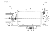
2 第2絶縁層
3 メタルコア(伝熱部材)
3’ 金属板
3a 凹状面
3b バリ(突出部)
3c 凸状面
3d ダレ(曲面部)
4 ヒートシンク(放熱部材)
4a 第1台座
4b 第2台座
4c 窪み
4h 螺合孔
5a〜5i 上表層の配線パターン
5j〜5n、5j’〜5n ’、5j”〜5n” 内層の配線パターン
5o〜5w 下表層の配線パターン
6a〜6e スルーホール(貫通導体)
7h 貫通孔
8 ねじ(螺合部材)
9a、9b FET(電子部品)
9c ディスクリート部品(電子部品)
9d〜9j チップコンデンサ(電子部品)
10 プリント基板
100 電子装置
L2 内層(第1内層)
L3、L4 内層(第2内層)
P 非重畳位置
Ra〜Rj 実装領域
Claims (9)
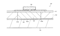
- 上面に電子部品の実装領域と配線パターンが設けられた第1絶縁層と、
前記第1絶縁層の下面に接するように設けられた第2絶縁層と、
前記実装領域と上下に重なるように前記第2絶縁層に埋設された伝熱部材と、を備えたプリント基板において、
前記伝熱部材は、金属板を切断加工することにより所定の形状に形成され、
前記伝熱部材の厚み方向に対して垂直な一方の外面は、その縁に曲面部が形成された凸状面であって、前記第1絶縁層の下面に接し、
前記伝熱部材の前記厚み方向に対して垂直な他方の外面は、その縁に突出部が形成された凹状面であって、前記第2絶縁層の下面から露出している、ことを特徴とするプリント基板。 - 請求項1に記載のプリント基板において、
前記伝熱部材の凹状面は、前記第2絶縁層の下方に設けられた放熱部材と接触する、ことを特徴とするプリント基板。 - 請求項1または請求項2に記載のプリント基板において、
前記第1絶縁層の熱伝導率は、前記第2絶縁層の熱伝導率より高く、
前記伝熱部材の熱伝導率は、前記第1絶縁層の熱伝導率より高い、ことを特徴とするプリント基板。 - 請求項1ないし請求項3のいずれかに記載のプリント基板において、
前記第2絶縁層は積層構造を有し、
前記第1絶縁層と前記第2絶縁層の間にある第1内層と、前記第2絶縁層の内部にある第2内層とに、それぞれ配線パターンが設けられ、
前記第1内層および前記第2内層の前記配線パターンは、前記伝熱部材に対して絶縁されている、ことを特徴とするプリント基板。 - 請求項1ないし請求項4のいずれかに記載のプリント基板において、
前記第2絶縁層の下面に、電子部品の実装領域と配線パターンが設けられ、
前記第2絶縁層の下面の前記実装領域と前記配線パターンは、前記伝熱部材に対して絶縁されている、ことを特徴とするプリント基板。 - 請求項5に記載のプリント基板において、
前記第1絶縁層と前記第2絶縁層とを貫通して、該両絶縁層にある前記配線パターンを接続する貫通導体をさらに備え、
前記貫通導体は、前記伝熱部材に対して絶縁されている、ことを特徴とするプリント基板。 - 請求項1ないし請求項6のいずれかに記載のプリント基板と、
前記プリント基板の前記実装領域に実装された発熱する電子部品と、
前記プリント基板の下方に設けられた放熱部材と、を備え、
前記放熱部材の上面に上方へ突出する第1台座を設け、
前記第1台座は、前記プリント基板に設けられた前記伝熱部材の前記凹状面における、前記突出部より内側の領域に接触する、ことを特徴とする電子装置。 - 請求項7に記載の電子装置において、
前記放熱部材の上面に、前記プリント基板の前記第2絶縁層の下面に設けられた電子部品および配線パターン、並びに前記伝熱部材の前記凹状面の前記突出部を避ける窪みを設けた、ことを特徴とする電子装置。 - 請求項7または請求項8に記載の電子装置において、
前記プリント基板の前記実装領域、前記配線パターン、および前記伝熱部材と重ならない非重畳領域に貫通孔を設け、
前記放熱部材の上面に前記第1台座とは別に、上方へ突出する第2台座を設け、
前記第2台座は、前記プリント基板の前記非重畳領域に接触し、
前記貫通孔と連通するように前記第2台座に螺合孔を設け、
前記螺合部材を前記プリント基板の上方から前記貫通孔へ貫通させて前記螺合孔に螺合することにより、前記放熱部材上に前記プリント基板を固定した、ことを特徴とする電子装置。
Priority Applications (4)
| Application Number | Priority Date | Filing Date | Title |
|---|---|---|---|
| JP2015118116A JP6501638B2 (ja) | 2015-06-11 | 2015-06-11 | 電子装置 |
| CN201610391060.XA CN106255308B (zh) | 2015-06-11 | 2016-06-03 | 印刷基板和电子装置 |
| DE102016209903.5A DE102016209903A1 (de) | 2015-06-11 | 2016-06-06 | Leiterplatte und Elektronikvorrichtung |
| US15/175,732 US9769916B2 (en) | 2015-06-11 | 2016-06-07 | Printed circuit board and electronic device |
Applications Claiming Priority (1)
| Application Number | Priority Date | Filing Date | Title |
|---|---|---|---|
| JP2015118116A JP6501638B2 (ja) | 2015-06-11 | 2015-06-11 | 電子装置 |
Publications (3)
| Publication Number | Publication Date |
|---|---|
| JP2017005131A true JP2017005131A (ja) | 2017-01-05 |
| JP2017005131A5 JP2017005131A5 (ja) | 2018-04-05 |
| JP6501638B2 JP6501638B2 (ja) | 2019-04-17 |
Family
ID=57395422
Family Applications (1)
| Application Number | Title | Priority Date | Filing Date |
|---|---|---|---|
| JP2015118116A Active JP6501638B2 (ja) | 2015-06-11 | 2015-06-11 | 電子装置 |
Country Status (4)
| Country | Link |
|---|---|
| US (1) | US9769916B2 (ja) |
| JP (1) | JP6501638B2 (ja) |
| CN (1) | CN106255308B (ja) |
| DE (1) | DE102016209903A1 (ja) |
Cited By (1)
| Publication number | Priority date | Publication date | Assignee | Title |
|---|---|---|---|---|
| JP2021089992A (ja) * | 2019-12-05 | 2021-06-10 | 三菱電機株式会社 | 電力変換装置 |
Families Citing this family (10)
| Publication number | Priority date | Publication date | Assignee | Title |
|---|---|---|---|---|
| TWI578416B (zh) * | 2015-09-18 | 2017-04-11 | 旭德科技股份有限公司 | 封裝載板及其製作方法 |
| US11025031B2 (en) | 2016-11-29 | 2021-06-01 | Leonardo Electronics Us Inc. | Dual junction fiber-coupled laser diode and related methods |
| CN108347820B (zh) * | 2017-01-25 | 2020-09-15 | 奥特斯(中国)有限公司 | 容纳部件的基底结构上的高导热涂层 |
| US11406004B2 (en) * | 2018-08-13 | 2022-08-02 | Leonardo Electronics Us Inc. | Use of metal-core printed circuit board (PCB) for generation of ultra-narrow, high-current pulse driver |
| DE102018213639A1 (de) * | 2018-08-14 | 2020-02-20 | Te Connectivity Germany Gmbh | Verfahren zum Anbringen wenigstens eines insbesondere stiftförmigen Kontaktelements auf einer Leiterbahn einer Leiterplatte, Stiftleiste zur Anbringung auf einer Leiterplatte, Verbindungsanordnung |
| BR112021010446A2 (pt) * | 2019-07-09 | 2021-08-24 | Juliano Anflor | Acoplamento térmico entre transistor e drivers de áudio com dissipador de calor |
| EP3792683A1 (en) | 2019-09-16 | 2021-03-17 | Leonardo Electronics US Inc. | Asymmetric input intensity hexagonal homogenizer |
| CN110519912B (zh) * | 2019-09-19 | 2020-11-06 | 生益电子股份有限公司 | 一种内嵌导热体的pcb制作方法及pcb |
| JP7469944B2 (ja) * | 2020-04-03 | 2024-04-17 | 株式会社小糸製作所 | プリント基板 |
| CN121310438A (zh) * | 2025-09-03 | 2026-01-09 | 广东世运电路科技股份有限公司 | 仿对称线路板叠构压合方法及线路板 |
Citations (4)
| Publication number | Priority date | Publication date | Assignee | Title |
|---|---|---|---|---|
| JPH06244303A (ja) * | 1993-01-27 | 1994-09-02 | Internatl Business Mach Corp <Ibm> | 温度管理可能な超小型電子パッケージ |
| JPH08228052A (ja) * | 1995-02-20 | 1996-09-03 | Mitsubishi Plastics Ind Ltd | 金属嵌合基板の製造方法 |
| JP2007088365A (ja) * | 2005-09-26 | 2007-04-05 | Sanyo Electric Co Ltd | 回路装置 |
| JP2014179416A (ja) * | 2013-03-14 | 2014-09-25 | Ngk Insulators Ltd | 放熱基板の製造方法、及び当該方法によって製造される放熱基板 |
Family Cites Families (32)
| Publication number | Priority date | Publication date | Assignee | Title |
|---|---|---|---|---|
| JP3163075B2 (ja) | 1999-07-30 | 2001-05-08 | 日本特殊陶業株式会社 | 金属製スティフナ付き配線基板 |
| US6744135B2 (en) * | 2001-05-22 | 2004-06-01 | Hitachi, Ltd. | Electronic apparatus |
| JP4022440B2 (ja) * | 2002-07-01 | 2007-12-19 | 株式会社オートネットワーク技術研究所 | 回路ユニット |
| JP3779721B1 (ja) | 2005-07-28 | 2006-05-31 | 新神戸電機株式会社 | 積層回路基板の製造方法 |
| JP4845090B2 (ja) | 2005-07-28 | 2011-12-28 | オンセミコンダクター・トレーディング・リミテッド | 回路装置の製造方法 |
| DE102005049872B4 (de) * | 2005-10-18 | 2010-09-23 | Continental Automotive Gmbh | IC-Bauelement mit Kühlanordnung |
| KR100735759B1 (ko) * | 2006-08-04 | 2007-07-06 | 삼성전자주식회사 | 다층 인쇄 회로 기판 |
| US20080224257A1 (en) * | 2007-03-12 | 2008-09-18 | Denso Corporation | Semiconductor device |
| JP5125241B2 (ja) | 2007-06-12 | 2013-01-23 | 三菱マテリアル株式会社 | パワーモジュール用基板の製造方法 |
| KR100896883B1 (ko) * | 2007-08-16 | 2009-05-14 | 주식회사 동부하이텍 | 반도체칩, 이의 제조방법 및 이를 가지는 적층 패키지 |
| US7829994B2 (en) * | 2007-09-24 | 2010-11-09 | Sixis, Inc. | Semiconductor substrate elastomeric stack |
| TW200915970A (en) * | 2007-09-27 | 2009-04-01 | Sanyo Electric Co | Circuit device, circuit module and outdoor equipment |
| US7738249B2 (en) * | 2007-10-25 | 2010-06-15 | Endicott Interconnect Technologies, Inc. | Circuitized substrate with internal cooling structure and electrical assembly utilizing same |
| JP2009290021A (ja) * | 2008-05-29 | 2009-12-10 | Toshiba Corp | 部品内蔵プリント配線板、同配線板の製造方法および電子機器 |
| CN104284533B (zh) * | 2008-09-28 | 2019-03-19 | 华为技术有限公司 | 多层电路板及其制作方法和通信设备 |
| US8276268B2 (en) * | 2008-11-03 | 2012-10-02 | General Electric Company | System and method of forming a patterned conformal structure |
| US20110085304A1 (en) * | 2009-10-14 | 2011-04-14 | Irvine Sensors Corporation | Thermal management device comprising thermally conductive heat spreader with electrically isolated through-hole vias |
| JP5546889B2 (ja) * | 2010-02-09 | 2014-07-09 | 日本電産エレシス株式会社 | 電子部品ユニット及びその製造方法 |
| KR101109359B1 (ko) * | 2010-06-14 | 2012-01-31 | 삼성전기주식회사 | 방열기판 및 그 제조방법 |
| DE102010060855A1 (de) * | 2010-11-29 | 2012-05-31 | Schweizer Electronic Ag | Elektronisches Bauteil, Verfahren zu dessen Herstellung und Leiterplatte mit elektronischem Bauteil |
| DE102011088969A1 (de) * | 2011-12-19 | 2013-06-20 | Robert Bosch Gmbh | Getriebesteuermodul |
| KR101330733B1 (ko) * | 2012-04-30 | 2013-11-20 | 삼성전자주식회사 | 초음파 프로브 |
| JP2014036033A (ja) * | 2012-08-07 | 2014-02-24 | Hitachi Automotive Systems Ltd | 半導体装置 |
| JP5885630B2 (ja) | 2012-09-21 | 2016-03-15 | 三菱電機株式会社 | プリント基板 |
| US20140133105A1 (en) * | 2012-11-09 | 2014-05-15 | Nvidia Corporation | Method of embedding cpu/gpu/logic chip into a substrate of a package-on-package structure |
| US9125299B2 (en) * | 2012-12-06 | 2015-09-01 | Apple Inc. | Cooling for electronic components |
| US20140160681A1 (en) * | 2012-12-07 | 2014-06-12 | Wintec Industries, Inc. | Discrete-Pin Printed-Circuit Mounting with Notches |
| KR102107038B1 (ko) * | 2012-12-11 | 2020-05-07 | 삼성전기주식회사 | 칩 내장형 인쇄회로기판과 그를 이용한 반도체 패키지 및 칩 내장형 인쇄회로기판의 제조방법 |
| US9258878B2 (en) * | 2013-02-13 | 2016-02-09 | Gerald Ho Kim | Isolation of thermal ground for multiple heat-generating devices on a substrate |
| ITMI20130872A1 (it) * | 2013-05-29 | 2013-08-28 | Mavel Srl | Dispositivo elettronico comprendente un circuito stampato |
| KR20150094135A (ko) * | 2014-02-10 | 2015-08-19 | 삼성전자주식회사 | 반도체 패키지 및 이의 제조방법 |
| US20150257249A1 (en) * | 2014-03-08 | 2015-09-10 | Gerald Ho Kim | Heat Sink With Protrusions On Multiple Sides Thereof And Apparatus Using The Same |
-
2015
- 2015-06-11 JP JP2015118116A patent/JP6501638B2/ja active Active
-
2016
- 2016-06-03 CN CN201610391060.XA patent/CN106255308B/zh active Active
- 2016-06-06 DE DE102016209903.5A patent/DE102016209903A1/de active Pending
- 2016-06-07 US US15/175,732 patent/US9769916B2/en active Active
Patent Citations (4)
| Publication number | Priority date | Publication date | Assignee | Title |
|---|---|---|---|---|
| JPH06244303A (ja) * | 1993-01-27 | 1994-09-02 | Internatl Business Mach Corp <Ibm> | 温度管理可能な超小型電子パッケージ |
| JPH08228052A (ja) * | 1995-02-20 | 1996-09-03 | Mitsubishi Plastics Ind Ltd | 金属嵌合基板の製造方法 |
| JP2007088365A (ja) * | 2005-09-26 | 2007-04-05 | Sanyo Electric Co Ltd | 回路装置 |
| JP2014179416A (ja) * | 2013-03-14 | 2014-09-25 | Ngk Insulators Ltd | 放熱基板の製造方法、及び当該方法によって製造される放熱基板 |
Cited By (1)
| Publication number | Priority date | Publication date | Assignee | Title |
|---|---|---|---|---|
| JP2021089992A (ja) * | 2019-12-05 | 2021-06-10 | 三菱電機株式会社 | 電力変換装置 |
Also Published As
| Publication number | Publication date |
|---|---|
| JP6501638B2 (ja) | 2019-04-17 |
| CN106255308A (zh) | 2016-12-21 |
| US20160366757A1 (en) | 2016-12-15 |
| US9769916B2 (en) | 2017-09-19 |
| CN106255308B (zh) | 2020-04-10 |
| DE102016209903A1 (de) | 2016-12-15 |
Similar Documents
| Publication | Publication Date | Title |
|---|---|---|
| JP6501638B2 (ja) | 電子装置 | |
| CN105744721B (zh) | 电路基板 | |
| JP6252871B2 (ja) | 回路構成体及び電気接続箱 | |
| CN102017135B (zh) | 带有在多个接触平面中的元器件的基板电路模块 | |
| EP3310140B1 (en) | Mounting assembly with a heatsink | |
| JP6249931B2 (ja) | 回路基板、回路基板の放熱構造、回路基板の製造方法 | |
| EP3093885A1 (en) | Semiconductor device and semiconductor device manufacturing method | |
| JP2018186143A (ja) | 回路基板モジュール、電子装置 | |
| US20200303112A1 (en) | MAGNETIC DEVICE and STACKED ELECTRONIC STRUCTURE | |
| CN105323951A (zh) | 印刷电路板及其制造方法 | |
| JP2014036085A (ja) | プリント配線板、プリント回路板及びプリント回路板の製造方法 | |
| KR102543495B1 (ko) | 다면 방열구조를 갖는 pcb 모듈, 및 이 모듈에 사용되는 방열 플레이트, 다층 pcb 어셈블리, 및 모듈 케이스 | |
| JP6381488B2 (ja) | 回路基板 | |
| JP6420966B2 (ja) | 配線基板及びその製造方法と電子部品装置 | |
| US9924590B2 (en) | Printed board and electronic apparatus | |
| CN206059386U (zh) | 布线基板以及电子装置 | |
| CN111031687A (zh) | 制备散热电路板的方法 | |
| JP6688487B2 (ja) | 回路基板、電子装置 | |
| WO2019194200A1 (ja) | 部品内蔵基板 | |
| JP2016076509A (ja) | 回路モジュール | |
| JP2020047690A (ja) | 電子回路装置 | |
| JP2016195192A (ja) | プリント基板、電子装置 | |
| JP2000299564A (ja) | 多層基板の放熱構造 | |
| JPH01143388A (ja) | 金属板をベースとしたプリント配線板 | |
| JP2016197691A (ja) | プリント基板、電子装置 |
Legal Events
| Date | Code | Title | Description |
|---|---|---|---|
| A521 | Request for written amendment filed |
Free format text: JAPANESE INTERMEDIATE CODE: A523 Effective date: 20180223 |
|
| A621 | Written request for application examination |
Free format text: JAPANESE INTERMEDIATE CODE: A621 Effective date: 20180223 |
|
| A977 | Report on retrieval |
Free format text: JAPANESE INTERMEDIATE CODE: A971007 Effective date: 20181025 |
|
| A131 | Notification of reasons for refusal |
Free format text: JAPANESE INTERMEDIATE CODE: A131 Effective date: 20181031 |
|
| A521 | Request for written amendment filed |
Free format text: JAPANESE INTERMEDIATE CODE: A523 Effective date: 20181220 |
|
| TRDD | Decision of grant or rejection written | ||
| A01 | Written decision to grant a patent or to grant a registration (utility model) |
Free format text: JAPANESE INTERMEDIATE CODE: A01 Effective date: 20190301 |
|
| A61 | First payment of annual fees (during grant procedure) |
Free format text: JAPANESE INTERMEDIATE CODE: A61 Effective date: 20190319 |
|
| R150 | Certificate of patent or registration of utility model |
Ref document number: 6501638 Country of ref document: JP Free format text: JAPANESE INTERMEDIATE CODE: R150 |
|
| S111 | Request for change of ownership or part of ownership |
Free format text: JAPANESE INTERMEDIATE CODE: R313117 |
|
| R360 | Written notification for declining of transfer of rights |
Free format text: JAPANESE INTERMEDIATE CODE: R360 |
|
| R360 | Written notification for declining of transfer of rights |
Free format text: JAPANESE INTERMEDIATE CODE: R360 |
|
| R371 | Transfer withdrawn |
Free format text: JAPANESE INTERMEDIATE CODE: R371 |
|
| S111 | Request for change of ownership or part of ownership |
Free format text: JAPANESE INTERMEDIATE CODE: R313117 |
|
| R350 | Written notification of registration of transfer |
Free format text: JAPANESE INTERMEDIATE CODE: R350 |
|
| R250 | Receipt of annual fees |
Free format text: JAPANESE INTERMEDIATE CODE: R250 |
|
| R250 | Receipt of annual fees |
Free format text: JAPANESE INTERMEDIATE CODE: R250 |
|
| R250 | Receipt of annual fees |
Free format text: JAPANESE INTERMEDIATE CODE: R250 |
|
| R250 | Receipt of annual fees |
Free format text: JAPANESE INTERMEDIATE CODE: R250 |
|
| R250 | Receipt of annual fees |
Free format text: JAPANESE INTERMEDIATE CODE: R250 |