JP2017005139A - Transistor - Google Patents
Transistor Download PDFInfo
- Publication number
- JP2017005139A JP2017005139A JP2015118380A JP2015118380A JP2017005139A JP 2017005139 A JP2017005139 A JP 2017005139A JP 2015118380 A JP2015118380 A JP 2015118380A JP 2015118380 A JP2015118380 A JP 2015118380A JP 2017005139 A JP2017005139 A JP 2017005139A
- Authority
- JP
- Japan
- Prior art keywords
- barrier layer
- gate electrode
- layer
- voltage
- drain electrode
- Prior art date
- Legal status (The legal status is an assumption and is not a legal conclusion. Google has not performed a legal analysis and makes no representation as to the accuracy of the status listed.)
- Pending
Links
Images






Classifications
-
- H—ELECTRICITY
- H10—SEMICONDUCTOR DEVICES; ELECTRIC SOLID-STATE DEVICES NOT OTHERWISE PROVIDED FOR
- H10D—INORGANIC ELECTRIC SEMICONDUCTOR DEVICES
- H10D64/00—Electrodes of devices having potential barriers
- H10D64/20—Electrodes characterised by their shapes, relative sizes or dispositions
- H10D64/23—Electrodes carrying the current to be rectified, amplified, oscillated or switched, e.g. sources, drains, anodes or cathodes
- H10D64/251—Source or drain electrodes for field-effect devices
- H10D64/257—Source or drain electrodes for field-effect devices for lateral devices wherein the source or drain electrodes are characterised by top-view geometrical layouts, e.g. interdigitated, semi-circular, annular or L-shaped electrodes
Landscapes
- Junction Field-Effect Transistors (AREA)
- Semiconductor Integrated Circuits (AREA)
Abstract
【課題】リカバリ特性の改善度を高めることができるトランジスタを提供する。
【解決手段】ゲート電極8の上部及びゲート電極8におけるドレイン電極7側の側面を覆うように絶縁膜層11上に形成されているFP12(金属板)を備える。また、FP12とソース電極6の間に抵抗値R1の抵抗14を接続するとともに、FP12とドレイン電極7の間に抵抗値R2の抵抗15を接続するように構成する。
【選択図】図2A transistor capable of improving the improvement degree of recovery characteristics is provided.
An FP 12 (metal plate) is provided on an insulating film layer 11 so as to cover an upper portion of the gate electrode 8 and a side surface of the gate electrode 8 on the drain electrode 7 side. Further, a resistor 14 having a resistance value R1 is connected between the FP 12 and the source electrode 6, and a resistor 15 having a resistance value R2 is connected between the FP 12 and the drain electrode 7.
[Selection] Figure 2
Description
この発明は、過電力の信号が入力された直後のドレイン電流の落ち込みを低減することが可能なトランジスタに関し、特に、窒化ガリウム(GaN)に代表される窒化物半導体の高電子移動度トランジスタ(HEMT:High Electron Mobility Transistor)に関するものである。 The present invention relates to a transistor capable of reducing a drop in drain current immediately after an overpower signal is input, and more particularly, a nitride semiconductor high electron mobility transistor (HEMT) represented by gallium nitride (GaN). : High Electron Mobility Transistor).
窒化ガリウム(GaN)は、ヒ化ガリウム(GaAs)やケイ素(Si)などの半導体材料よりも、耐圧や飽和速度の観点で優れている特徴を有している。
そのため、窒化ガリウム(GaN)は、高出力高周波増幅器やパワースイッチ回路に用いられることが多いが、近年、窒化ガリウム(GaN)を低雑音増幅器(LNA)に用いる研究開発が行われている。
Gallium nitride (GaN) has characteristics that are superior in terms of breakdown voltage and saturation speed over semiconductor materials such as gallium arsenide (GaAs) and silicon (Si).
For this reason, gallium nitride (GaN) is often used in high-power high-frequency amplifiers and power switch circuits, but in recent years, research and development using gallium nitride (GaN) for low-noise amplifiers (LNA) has been conducted.
例えば、送受信モジュールにおいては、過電力の信号である妨害波から低雑音増幅器を守るため、一般的に、低雑音増幅器の前段に保護スイッチ回路が挿入されるが、低雑音増幅器として、高耐圧な窒化物半導体の低雑音増幅器(GaNLNA)を用いれば、保護スイッチ回路を取り除くことができる。
保護スイッチ回路を取り除くことができれば、保護スイッチ回路での電力損失を低減することができるため、送受信モジュールとしての雑音指数(NF)を改善することができる。
For example, in a transmission / reception module, a protection switch circuit is generally inserted in front of a low noise amplifier in order to protect the low noise amplifier from an interference wave that is an overpower signal. If a nitride semiconductor low noise amplifier (GaNLNA) is used, the protection switch circuit can be removed.
If the protection switch circuit can be removed, power loss in the protection switch circuit can be reduced, so that the noise figure (NF) as a transmission / reception module can be improved.
ただし、スイッチレスでGaNLNAを用いる場合、過電力の信号がGaNLNAに直接入力されることがあるため、過電力の信号が入力された直後においても、GaNLNAが正常に動作することが求められる。
一般的に、過電力の信号がGaNLNAに入力された直後は、窒化ガリウム(GaN)のトラップ(半導体の格子欠損)の影響でドレイン電流が減少し、その後、過渡的に或る時定数を持って、減少したドレイン電流が回復するという現象が生じる。この現象はリカバリ特性と呼ばれる。
過電力の信号が入力された直後のドレイン電流が減少している状態は、雑音指数(NF)や利得が低下するため、GaNLNAが正常に動作していないことを意味する。
However, when the switchless GaNLNA is used, an overpower signal may be directly input to the GaNLNA. Therefore, the GaNLNA is required to operate normally immediately after the overpower signal is input.
In general, immediately after an overpower signal is input to GaN LNA, the drain current decreases due to the influence of gallium nitride (GaN) traps (semiconductor lattice defects), and then has a transient time constant. As a result, the reduced drain current recovers. This phenomenon is called recovery characteristics.
A state in which the drain current immediately after the overpower signal is input means that the noise figure (NF) and the gain are reduced, so that the GaN LNA is not operating normally.
窒化物半導体の高電子移動度トランジスタであるGaNHEMTのリカバリ特性(トラップ)を改善する一般的な技術として、ソースフィールドプレート構造(SFP構造)がある。
例えば、以下の非特許文献1には、SFP構造を有するGaNHEMTが開示されている。
このGaNHEMTでは、チャネル層(GaN buffer)の上にスペーサ層(AlN)及びバリア層(AlGaN)が結晶成長され、バリア層上に窒化膜(Si3N4)、電極(ソース電極、ゲート電極、ドレイン電極)が形成され、ゲート電極の上に窒化膜(Si3N4)が形成されている。
また、ソース電極に接続されている金属板が、ゲート電極の上部に形成されている窒化膜(Si3N4)上に形成されている。この構造がSFP構造と呼ばれ、ゲート電極の上部の金属板はソースフィールドプレート(SFP)と呼ばれる。
As a general technique for improving the recovery characteristic (trap) of a GaN HEMT which is a high electron mobility transistor of a nitride semiconductor, there is a source field plate structure (SFP structure).
For example, Non-Patent
In this GaN HEMT, a spacer layer (AlN) and a barrier layer (AlGaN) are grown on a channel layer (GaN buffer), and a nitride film (Si 3 N 4 ), electrodes (source electrode, gate electrode, A drain electrode) is formed, and a nitride film (Si 3 N 4 ) is formed on the gate electrode.
Further, a metal plate connected to the source electrode is formed on a nitride film (Si 3 N 4 ) formed on the gate electrode. This structure is called an SFP structure, and the metal plate above the gate electrode is called a source field plate (SFP).
このソースフィールドプレートは、グランドに接地されているソース電極と接続されているため、チャネル層に形成される2次元電子ガスからゲート電極に向かう電界の一部がソースフィールドプレートに分散される。
その結果、ゲート電極における電界集中が緩和されてトラップの影響が低減するため、リカバリ特性が改善される。
Since the source field plate is connected to the source electrode grounded to the ground, a part of the electric field from the two-dimensional electron gas formed in the channel layer to the gate electrode is dispersed in the source field plate.
As a result, the electric field concentration in the gate electrode is relaxed and the influence of traps is reduced, so that the recovery characteristics are improved.
従来のトランジスタは以上のように構成されているので、SFP構造がトラップの影響を低減して、リカバリ特性を改善している。しかし、SFP構造を有するだけでは、トラップの影響を十分に低減することができず、リカバリ特性の改善度が小さいという課題があった。 Since the conventional transistor is configured as described above, the SFP structure reduces the influence of traps and improves recovery characteristics. However, the trap structure cannot be sufficiently reduced only by having the SFP structure, and there is a problem that the improvement degree of the recovery characteristics is small.
この発明は上記のような課題を解決するためになされたもので、リカバリ特性の改善度を高めることができるトランジスタを得ることを目的とする。 The present invention has been made to solve the above-described problems, and an object of the present invention is to obtain a transistor capable of increasing the improvement in recovery characteristics.
この発明に係るトランジスタは、電子が流れるチャネル層と、2次元電子ガスをチャネル層に形成するためにチャネル層の上部に形成されているバリア層と、バリア層の上部に形成され、グランドに接地されているソース電極と、バリア層の上部に形成され、第1の電圧が印加されるドレイン電極と、バリア層の上部に形成され、第2の電圧が印加されるゲート電極と、ソース電極及びドレイン電極が形成されている領域を除くバリア層の上部とゲート電極を覆っている絶縁膜層と、ゲート電極の上部及びゲート電極におけるドレイン電極側の側面を覆うように絶縁膜層上に形成されている金属板と、一端が金属板と接続され、他端がソース電極と接続されている第1の抵抗と、一端が金属板と接続され、他端がドレイン電極と接続されている第2の抵抗とを備えるようにしたものである。 The transistor according to the present invention includes a channel layer through which electrons flow, a barrier layer formed above the channel layer to form a two-dimensional electron gas in the channel layer, and formed above the barrier layer and grounded to ground. A source electrode formed on the barrier layer, to which a first voltage is applied; a gate electrode formed on the barrier layer to which a second voltage is applied; a source electrode; It is formed on the insulating film layer so as to cover the upper part of the barrier layer excluding the region where the drain electrode is formed, the insulating film layer covering the gate electrode, and the upper part of the gate electrode and the side surface of the gate electrode on the drain electrode side. A metal plate, one end connected to the metal plate, the other end connected to the source electrode, one end connected to the metal plate, and the other end connected to the drain electrode. It is obtained by so and a second resistor.
この発明によれば、ゲート電極の上部及びゲート電極におけるドレイン電極側の側面を覆うように絶縁膜層上に形成されている金属板を備え、金属板とソース電極の間に第1の抵抗を接続するとともに、金属板とドレイン電極の間に第2の抵抗を接続するように構成したので、リカバリ特性の改善度を高めることができる効果がある。 According to the present invention, the metal plate formed on the insulating film layer so as to cover the upper portion of the gate electrode and the side surface of the gate electrode on the drain electrode side is provided, and the first resistor is provided between the metal plate and the source electrode. Since the connection is made and the second resistor is connected between the metal plate and the drain electrode, there is an effect that the improvement degree of the recovery characteristic can be increased.
以下、この発明をより詳細に説明するために、この発明を実施するための形態について、添付の図面にしたがって説明する。 Hereinafter, in order to describe the present invention in more detail, modes for carrying out the present invention will be described with reference to the accompanying drawings.
実施の形態1.
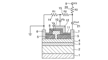
図1はこの発明の実施の形態1によるトランジスタを示す回路図であり、図2はこの発明の実施の形態1によるトランジスタを示す断面図である。
図1及び図2は、トランジスタが、窒化物半導体の高電子移動度トランジスタ(GaNHEMT)である例を示している。実際には、素子分離領域や配線などがあるが、本発明の動作と関連がないため、図1及び図2では省略している。
FIG. 1 is a circuit diagram showing a transistor according to
1 and 2 show an example in which the transistor is a nitride semiconductor high electron mobility transistor (GaNHEMT). Actually, there are element isolation regions and wirings, but they are not shown in FIGS. 1 and 2 because they are not related to the operation of the present invention.
図1及び図2において、基板1はサファイア、炭化ケイ素(SiC)、ケイ素(Si)、窒化ガリウム(GaN)などを用いて形成されている。一般的には、熱伝導率が良好な半絶縁性SiC基板が利用されるが、半導体基板として非常に一般的なSi基板も価格が安いため、良く用いられる。
バッファ層2はチャネル層3の結晶性の向上や、電子をチャネル層3に閉じ込める目的で、基板1とチャネル層3との間に挿入される層であり、例えば、窒化アルミニウム(AlN)、窒化アルミニウムガリウム(AlGaN)、窒化ガリウム(GaN)とインジウム窒化ガリウム(InGaN)の混晶組成、窒化アルミニウム(AlN)と窒化アルミニウムガリウム(AlGaN)の混晶組成などの材料が用いられる。また、それらの材料の超格子などが用いられる。
1 and 2, the
The
チャネル層3はバッファ層2の上部に形成され、トランジスタの動作に必要な電子(電流)が流れる層である。
チャネル層3としては、例えば、窒化ガリウム(GaN)が用いられるが、インジウム窒化ガリウム(InGaN)や窒化アルミニウムガリウム(AlGaN)のほか、インジウム窒化ガリウム(InGaN)と窒化アルミニウムガリウム(AlGaN)の多層構造も使うことができる。
また、チャネル層3には、不純物をドープすることでゲート電極8の制御性を向上させることができ、この不純物としては、半導体を半絶縁性にする遷移金属である鉄(Fe)や銅(Cu)などが用いられる。不純物ドープのプロファイルはいかなるものでもよい。
The
As the
In addition, the
バリア層4は2次元電子ガスをチャネル層3に形成するために、チャネル層3の上部に形成されている。
バリア層4としては、例えば、窒化アルミニウムガリウム(AlGaN)の単層が用いられるが、イリジウム(In)、アルミニウム(Al)及びガリウム(Ga)の中のいずれか1つ以上と窒素(N)を含んでいるものであればよい。
また、組成、層厚や不純物濃度が異なる複数の窒化アルミニウムガリウム(AlGaN)、窒化アルミニウムガリウム(AlGaN)と窒化ガリウム(GaN)又は窒化アルミニウム(AlN)の組み合わせであってもよい。
なお、チャネル層3とバリア層4が接触する界面は、チャネル層3よりバンドギャップが広いヘテロ接合で形成させる。
The
As the
A combination of a plurality of aluminum gallium nitrides (AlGaN), aluminum gallium nitride (AlGaN) and gallium nitride (GaN), or aluminum nitride (AlN) having different compositions, layer thicknesses, and impurity concentrations may be used.
Note that the interface between the
絶縁膜層5はバリア層4の表面のトラップを抑制するために、バリア層4の上部に形成されている。
絶縁膜層5としては、例えば、窒化ケイ素(SiN)や一酸化ケイ素(SiO)などのドナーの役割を果たすケイ素(Si)を含んでいる絶縁膜が用いられる。絶縁膜層5がケイ素(Si)を含んでいれば、ドナーとしてバリア層4に電子を供給してバリア層4の表面上のトラップ数を減らすことができる。図2の例では、絶縁膜層5がゲート電極8の下部の一部(図中、ゲート電極8の左下及び右下の部分)に設けられている構造であるが、絶縁膜層5がゲート電極8の下部の一部に設けられていなくても、同様の効果が得られる。
The
As the
ソース電極6及びドレイン電極7はチャネル層3中の電子(電流)をHEMTの外に取出すための電極である。
ソース電極6はバリア層4の上部に形成され、グランドに接地されている。
ドレイン電極7はバリア層4の上部に形成され、第1の電圧である電圧Vdが印加されている端子9と接続されている。
なお、ソース電極6及びドレイン電極7は、チャネル層3に形成される2次元電子ガスとの間の抵抗ができるだけ小さくなるように形成される。図2の例では、バリア層4と接するように形成されているが、2次元電子ガスと直接的に接するように形成されていてもよい。また、ソース電極6及びドレイン電極7の下側には、n+領域が形成されていてもよい。
The
The
The
The
ゲート電極8はバリア層4の上部に形成され、バリア層4とショットキー接触する金属を含んでいる。ゲート電極8は第2の電圧である電圧Vgが印加されている端子10と接続されている。
なお、ゲート電極8の下側の2DEG濃度(2次元電子ガスの濃度)を制御することで、トランジスタ動作を実現することができる。
The
The transistor operation can be realized by controlling the 2DEG concentration (the concentration of the two-dimensional electron gas) on the lower side of the
絶縁膜層11はソース電極6及びドレイン電極7が形成されている領域を除くバリア層4の上部とゲート電極8を覆うように形成されている。
絶縁膜層11は、カバレッジのための材料として、例えば、窒化ケイ素(SiN)、二酸化ケイ素(SiO2)、酸化アルミニウム(Al2O3)が用いられる。
The insulating
For example, silicon nitride (SiN), silicon dioxide (SiO 2 ), or aluminum oxide (Al 2 O 3 ) is used for the insulating
FP12はゲート電極8の上部及びゲート電極8におけるドレイン電極7側の側面を覆うように絶縁膜層11上に形成されている金属板である。
ゲート電極8の上部だけでなく、ドレイン電極7側の側面にもFP12が取り付けられていなければ、トラップの影響を低減して、リカバリ特性を改善する効果が得られないため、図2の例では、FP12の形状がL字型になっている。図2の例では、ゲート電極8におけるソース電極6の側面にはFP12が取り付けられていないが、FP12をソース電極6の側面に取り付けても、ドレイン電極7側の側面に取り付けていれば、リカバリ特性を改善する効果が得られる。
The
If the
抵抗14は一端がFP12と接続され、他端がソース電極6と接続されている抵抗値R1の第1の抵抗である。
抵抗15は一端がFP12と接続され、他端がドレイン電極7と接続されている抵抗値R2の第2の抵抗である。
The
The
図3はこの発明の実施の形態1によるトランジスタを示す上面図である。図2の断面図は、図3における点線部の断面図である。
図3の例では、抵抗14,15がチップ抵抗で構成されており、抵抗14はワイヤ16を介してソース電極6と接続され、ワイヤ17を介してFP12と接続されている。
抵抗15はワイヤ18を介してFP12と接続され、ワイヤ19を介してドレイン電極7と接続されている。
なお、図3では、ソース電極6を設置するためのビアが、ソース電極6の直下に直接形成されるビアホール構造(ISV:Individual Source Viahole)であるが、ビアの構造はISVに限るものではない。
FIG. 3 is a top view showing a transistor according to the first embodiment of the present invention. 2 is a cross-sectional view taken along a dotted line in FIG.
In the example of FIG. 3, the
The
In FIG. 3, the via for installing the
非特許文献1に開示されているGaNHEMTと、この実施の形態1のGaNHEMTとの構造を比較すると、非特許文献1に開示されているGaNHEMTでは、図2のFP12に相当するソースフィールドプレート(SFP)が、グランドに接地されているソース電極と直接接続されている構造であるが、この実施の形態1のGaNHEMTでは、FP12が、グランドに接地されているソース電極6と抵抗14を介して接続され、また、ドレイン電極7と抵抗15を介して接続されている構造である点で相違している。
なお、この実施の形態1のGaNHEMTは、低雑音増幅器(GaNLNA)に限らず、例えば、高出力増幅器など、トラップによるリカバリ特性の劣化が問題となる増幅器に対して有効である。
Comparing the structure of the GaN HEMT disclosed in
Note that the GaN HEMT according to the first embodiment is not limited to a low noise amplifier (GaNLNA) but is effective for an amplifier in which deterioration of recovery characteristics due to a trap is a problem, such as a high output amplifier.
次に動作について説明する。
ゲート電極8の上部及びゲート電極8におけるドレイン電極7側の側面を覆うように、FP12を絶縁膜層11上に形成することで、チャネル層3に形成される2次元電子ガスからゲート電極8に向かう電界の一部がFP12に分散されるため、ゲート電極8における電界集中が緩和されてトラップの影響が低減される。その結果、リカバリ特性が改善される。
このとき、FP12が抵抗14を介さずに、グランドに接地されているソース電極6と直接接続されている構造(以下、「従来構造」と称する)の場合、FP12の電位が0Vに固定されるため、リカバリ特性の改善効果が小さいものとなる。
しかし、この実施の形態では、FP12が抵抗14を介してソース電極6と接続されており、また、ドレイン電極7と抵抗15を介して接続されている。このため、FP12には、プラスの電圧Vfpが印加される構造になっている。
Next, the operation will be described.
By forming the
At this time, in the case of a structure in which the
However, in this embodiment, the
プラスの電圧VfpがFP12に印加されると、バリア層4の表面の電界が低減されて、バリア層4の表面のトラップに電子が捕まり難くなる。そのため、従来構造と比べて、トラップの影響が低減されて、リカバリ特性が改善される。
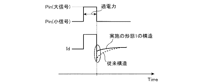
図4はこの発明の実施の形態1によるトランジスタのリカバリ特性を示す説明図である。
過電力の信号(Pin)がGaNHEMTに入力された直後は、図4に示すように、窒化ガリウム(GaN)のトラップの影響でドレイン電流Idが減少し、その後、ドレイン電流Idが徐々に回復するという現象が生じる。
従来構造では、ドレイン電流Idの減少が大きいのに対して、この実施の形態1の構造では、バリア層4の表面のトラップに電子が捕まり難くなっているため、ドレイン電流Idの減少が小さくなっており、リカバリ特性が改善されている。
When the positive voltage Vfp is applied to the
FIG. 4 is an explanatory diagram showing the recovery characteristics of the transistor according to the first embodiment of the present invention.
Immediately after the overpower signal (Pin) is input to the GaN HEMT, as shown in FIG. 4, the drain current Id decreases due to the trap of gallium nitride (GaN), and then the drain current Id gradually recovers. The phenomenon that occurs.
In the conventional structure, the drain current Id is greatly reduced. On the other hand, in the structure of the first embodiment, since it is difficult for electrons to be trapped in the traps on the surface of the
この実施の形態1でのリカバリ特性の改善をデバイスシミュレーションで検証しており、以下、この検証内容について説明する。
図5は実施の形態1の構造と従来構造において、図2の絶縁膜層5とバリア層4の界面から0.5nm下の電界分布(以下、「バリア層表面の電界分布」と称する)のシミュレーション結果を示す説明図である。
このときのバイアス条件は、ドレイン電圧Vd=30V、ゲート電圧Vg=−5Vである。ただし、従来構造では、FP12が抵抗14を介さずに、グランドに接地されているソース電極6と直接接続されているため、Vfp=0Vであるが、実施の形態1の構造では、Vfp=2Vである。
図5から明らかなように、バリア層表面の電界分布が、従来構造より実施の形態1の構造の方が低くなっており、トラップの影響を低減できていることが分かる。
The improvement of the recovery characteristic in the first embodiment is verified by device simulation, and the verification contents will be described below.
5 shows the electric field distribution 0.5 nm below the interface between the insulating
The bias conditions at this time are a drain voltage Vd = 30V and a gate voltage Vg = −5V. However, in the conventional structure, since the
As is apparent from FIG. 5, the electric field distribution on the barrier layer surface is lower in the structure of the first embodiment than in the conventional structure, and it can be seen that the influence of traps can be reduced.
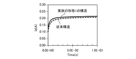
図6及び図7はドレイン電流Idのリカバリ特性のシミュレーション結果を示す説明図である。
図7は図6の縦軸に示すドレイン電流IdをLog表示したものである。
図6及び図7から明らかなように、従来構造より実施の形態1の構造の方が、ドレイン電流Idの低減が小さいため、リカバリ特性が改善されていることが分かる。
6 and 7 are explanatory diagrams showing simulation results of the recovery characteristics of the drain current Id.
FIG. 7 is a log representation of the drain current Id shown on the vertical axis of FIG.
As is apparent from FIGS. 6 and 7, it can be seen that the recovery characteristic is improved in the structure of the first embodiment because the reduction in the drain current Id is smaller than in the conventional structure.
次に、抵抗14,15の抵抗値R1,R2について説明する。
抵抗14,15の抵抗値R1,R2は、10kΩ以上の高抵抗である必要がある。抵抗14,15の抵抗値R1,R2が低いと、ドレイン電流Idが抵抗14,15側に流れてしまうためである。
また、FP12に印加される電圧Vfpは、ドレイン電圧Vdが抵抗14と抵抗15によって分圧された電圧であるため、下記の式(1)のように表される。
FP12に印加される電圧Vfpは、トラップの影響が低減される効果を得るにはプラスの電圧である必要があるが、2Vを超えると、DC特性に影響がでる可能性があるため、下記の式(2)の条件を満足していることが望ましい。
式(1)(2)より、抵抗値R1に対する抵抗値R2の比が、下記の式(3)の条件を満足している必要がある。
The resistance values R1 and R2 of the
Further, the voltage Vfp applied to the
The voltage Vfp applied to the
From the expressions (1) and (2), the ratio of the resistance value R2 to the resistance value R1 needs to satisfy the condition of the following expression (3).
以上で明らかなように、この実施の形態1によれば、ゲート電極8の上部及びゲート電極8におけるドレイン電極7側の側面を覆うように絶縁膜層11上に形成されているFP12を備え、FP12とソース電極6の間に抵抗14を接続するとともに、FP12とドレイン電極7の間に抵抗15を接続するように構成したので、リカバリ特性の改善度を高めることができる効果を奏する。
As apparent from the above, according to the first embodiment, the
実施の形態2.
上記実施の形態1では、抵抗14,15がチップ抵抗で構成されており、抵抗14がワイヤ16,17によってソース電極6とFP12との間に接続され、また、抵抗15がワイヤ18,19によってFP12とドレイン電極7との間に接続されているものを示したが、抵抗14,15が基板1上にイオン注入抵抗として形成されているものであってもよい。
In the first embodiment, the
図8はこの発明の実施の形態2によるトランジスタを示す上面図であり、図8において、図3と同一符号は同一または相当部分を示すので説明を省略する。
図8では、抵抗14,15をモノシリックマイクロ波集積回路(MMIC)として、トランジスタと同じ基板1上に形成している構造になっている。
また、抵抗14,15は、不純物イオンが注入されることで、n+層が半導体層で形成されて作られるイオン注入抵抗である。
この実施の形態2では、トランジスタと同じ基板1上に抵抗14,15が形成されるため、上記実施の形態1よりも小型化を図ることができる。
FIG. 8 is a top view showing a transistor according to the second embodiment of the present invention. In FIG. 8, the same reference numerals as those in FIG.
In FIG. 8,
The
In the second embodiment, since the
実施の形態3.
図9はこの発明の実施の形態3によるトランジスタを示す回路図であり、図10はこの発明の実施の形態3によるトランジスタを示す断面図である。
図9及び図10において、図1及び図2と同一符号は同一または相当部分を示すので説明を省略する。
抵抗20は電圧Vdが印加されている端子9とドレイン電極7の端子21との間に接続されている抵抗値R3の第3の抵抗である。
なお、抵抗14,15,20は、上記実施の形態1のようにチップ抵抗で形成してもよいし、上記実施の形態2のように、MMICとしてイオン注入抵抗で形成してもよい。
抵抗20を実装している点以外は、上記実施の形態1,2と同様である。
FIG. 9 is a circuit diagram showing a transistor according to
9 and 10, the same reference numerals as those in FIGS. 1 and 2 indicate the same or corresponding parts, and thus description thereof is omitted.
The
The
Except that the
次に動作について説明する。
図11はこの発明の実施の形態3によるトランジスタのリカバリ特性を示す説明図である。
図11では、実施の形態1,3の構造のリカバリ特性と、従来構造のリカバリ特性とを示している。
従来構造では、FP12が抵抗14を介さずに、グランドに接地されているソース電極6と直接接続されているため、Vfp=0Vである。
上記実施の形態1の構造では、常にプラスの電圧VfpがFP12に印加されている。
Next, the operation will be described.
FIG. 11 is an explanatory diagram showing the recovery characteristics of the transistor according to the third embodiment of the present invention.
FIG. 11 shows the recovery characteristics of the structures of the first and third embodiments and the recovery characteristics of the conventional structure.
In the conventional structure, since the
In the structure of the first embodiment, a positive voltage Vfp is always applied to the
この実施の形態3では、電圧Vdが印加されている端子9とドレイン電極7の端子21との間に抵抗20が接続されているため、過電力の信号(Pin)がGaNHEMTに入力されているときは、ドレイン電流Idが大きくなるため、端子21の電圧Voutが低下して、FP12に印加される電圧Vfpも低下する。
ただし、過電力の信号(Pin)がGaNHEMTに入力された直後は、ドレイン電流Idが急激に低下するため、端子21の電圧Voutが上昇して、FP12に印加される電圧Vfpも上昇する。
FP12に印加される電圧Vfpが高くなると、FP12による電界低減効果が大きくなり、トラップ効果が低減される。
このため、図11に示すように、従来構造や上記実施の形態1の構造よりも、この実施の形態3の方が、リカバリ特性が改善される。
In the third embodiment, since the
However, immediately after the overpower signal (Pin) is input to the GaN HEMT, the drain current Id rapidly decreases, so the voltage Vout at the terminal 21 increases and the voltage Vfp applied to the
When the voltage Vfp applied to the
For this reason, as shown in FIG. 11, the recovery characteristics of the third embodiment are improved compared to the conventional structure and the structure of the first embodiment.
実施の形態4.
上記実施の形態1〜3では、抵抗14,15を接続することで、プラスの電圧VfpがFP12に印加されるものを示したが、過電力の信号(Pin)が入力されるタイミングでプラスの電圧VfpがFP12に印加されるようにしてもよい。
In the first to third embodiments, a case where the positive voltage Vfp is applied to the
図12はこの発明の実施の形態4によるトランジスタを示す上面図であり、図12において、図3と同一符号は同一または相当部分を示すので説明を省略する。
スイッチング回路22は過電力の信号(Pin)が入力されるタイミング(入力信号の電力が増加するタイミング)で、プラスの電圧VfpをFP12に印加する回路である。
即ち、スイッチング回路22は、過電力の信号(Pin)が入力されるタイミングで、プラスの電圧VfpをFP12に印加するために、電圧Vfpをパルス制御する回路である。
12 is a top view showing a transistor according to
The switching
That is, the switching
この実施の形態4では、スイッチング回路22が、過電力の信号(Pin)が入力されるタイミングで、プラスの電圧VfpをFP12に印加するため、上記実施の形態1〜3と同様に、過電力の信号(Pin)が入力された直後のトラップ効果の低減が図られ、リカバリ特性が改善される。
したがって、上記実施の形態1〜3と同様に、リカバリ特性の改善度を高めることができる効果が得られる。また、端子9に印加される電圧Vdに依存せずに、電圧VfpをFP12に印加することができる。
In the fourth embodiment, since the switching
Therefore, as in the first to third embodiments, an effect of improving the improvement degree of the recovery characteristic can be obtained. Further, the voltage Vfp can be applied to the
なお、本願発明はその発明の範囲内において、各実施の形態の自由な組み合わせ、あるいは各実施の形態の任意の構成要素の変形、もしくは各実施の形態において任意の構成要素の省略が可能である。 In the present invention, within the scope of the invention, any combination of the embodiments, or any modification of any component in each embodiment, or omission of any component in each embodiment is possible. .
1 基板、2 バッファ層、3 チャネル層、4 バリア層、5 絶縁膜層、6 ソース電極、7 ドレイン電極、8 ゲート電極、9,10 端子、11 絶縁膜層、12 FP(金属板)、14 抵抗(第1の抵抗)、15 抵抗(第2の抵抗)、16,17,18,19 ワイヤ、20 抵抗(第3の抵抗)、21 端子、22 スイッチング回路。 1 substrate, 2 buffer layer, 3 channel layer, 4 barrier layer, 5 insulating film layer, 6 source electrode, 7 drain electrode, 8 gate electrode, 9, 10 terminal, 11 insulating film layer, 12 FP (metal plate), 14 Resistance (first resistance), 15 Resistance (second resistance), 16, 17, 18, 19 wire, 20 Resistance (third resistance), 21 terminals, 22 Switching circuit.
Claims (6)
2次元電子ガスを前記チャネル層に形成するために前記チャネル層の上部に形成されているバリア層と、
前記バリア層の上部に形成され、グランドに接地されているソース電極と、
前記バリア層の上部に形成され、第1の電圧が印加されるドレイン電極と、
前記バリア層の上部に形成され、第2の電圧が印加されるゲート電極と、
前記ソース電極及び前記ドレイン電極が形成されている領域を除く前記バリア層の上部と前記ゲート電極を覆っている絶縁膜層と、
前記ゲート電極の上部及び前記ゲート電極における前記ドレイン電極側の側面を覆うように前記絶縁膜層上に形成されている金属板と、
一端が前記金属板と接続され、他端が前記ソース電極と接続されている第1の抵抗と、
一端が前記金属板と接続され、他端が前記ドレイン電極と接続されている第2の抵抗と
を備えたトランジスタ。 A channel layer through which electrons flow;
A barrier layer formed on top of the channel layer to form a two-dimensional electron gas in the channel layer;
A source electrode formed on the barrier layer and grounded;
A drain electrode formed on the barrier layer and applied with a first voltage;
A gate electrode formed on the barrier layer and applied with a second voltage;
An upper part of the barrier layer excluding a region where the source electrode and the drain electrode are formed and an insulating film layer covering the gate electrode;
A metal plate formed on the insulating film layer so as to cover an upper portion of the gate electrode and a side surface of the gate electrode on the drain electrode side;
A first resistor having one end connected to the metal plate and the other end connected to the source electrode;
And a second resistor having one end connected to the metal plate and the other end connected to the drain electrode.
2次元電子ガスを前記チャネル層に形成するために前記チャネル層の上部に形成されているバリア層と、
前記バリア層の上部に形成され、グランドに接地されているソース電極と、
前記バリア層の上部に形成され、第1の電圧が印加されるドレイン電極と、
前記バリア層の上部に形成され、第2の電圧が印加されるゲート電極と、
前記ソース電極及び前記ドレイン電極が形成されている領域を除く前記バリア層の上部と前記ゲート電極を覆っている絶縁膜層と、
前記ゲート電極の上部及び前記ゲート電極における前記ドレイン電極側の側面を覆うように前記絶縁膜層上に形成されている金属板と、
入力信号の電力が増加するタイミングでプラスの電圧を前記金属板に印加するスイッチング回路と
を備えたトランジスタ。 A channel layer through which electrons flow;
A barrier layer formed on top of the channel layer to form a two-dimensional electron gas in the channel layer;
A source electrode formed on the barrier layer and grounded;
A drain electrode formed on the barrier layer and applied with a first voltage;
A gate electrode formed on the barrier layer and applied with a second voltage;
An upper part of the barrier layer excluding a region where the source electrode and the drain electrode are formed and an insulating film layer covering the gate electrode;
A metal plate formed on the insulating film layer so as to cover an upper portion of the gate electrode and a side surface of the gate electrode on the drain electrode side;
A switching circuit that applies a positive voltage to the metal plate at a timing when the power of the input signal increases.
Priority Applications (1)
| Application Number | Priority Date | Filing Date | Title |
|---|---|---|---|
| JP2015118380A JP2017005139A (en) | 2015-06-11 | 2015-06-11 | Transistor |
Applications Claiming Priority (1)
| Application Number | Priority Date | Filing Date | Title |
|---|---|---|---|
| JP2015118380A JP2017005139A (en) | 2015-06-11 | 2015-06-11 | Transistor |
Publications (1)
| Publication Number | Publication Date |
|---|---|
| JP2017005139A true JP2017005139A (en) | 2017-01-05 |
Family
ID=57752900
Family Applications (1)
| Application Number | Title | Priority Date | Filing Date |
|---|---|---|---|
| JP2015118380A Pending JP2017005139A (en) | 2015-06-11 | 2015-06-11 | Transistor |
Country Status (1)
| Country | Link |
|---|---|
| JP (1) | JP2017005139A (en) |
Cited By (2)
| Publication number | Priority date | Publication date | Assignee | Title |
|---|---|---|---|---|
| US11424330B2 (en) | 2018-10-03 | 2022-08-23 | Mitsubishi Electric Corporation | Field-effect transistor |
| JP2022550464A (en) * | 2019-10-02 | 2022-12-01 | ウルフスピード インコーポレイテッド | Radio frequency transistor amplifier with engineered intrinsic capacitance for improved performance |
Citations (4)
| Publication number | Priority date | Publication date | Assignee | Title |
|---|---|---|---|---|
| JP2010278280A (en) * | 2009-05-29 | 2010-12-09 | Toshiba Corp | High frequency semiconductor device |
| WO2013027722A1 (en) * | 2011-08-22 | 2013-02-28 | ルネサスエレクトロニクス株式会社 | Semiconductor device |
| JP2014086491A (en) * | 2012-10-22 | 2014-05-12 | Fujitsu Ltd | Control circuit of transistor and power supply device |
| JP2015023098A (en) * | 2013-07-17 | 2015-02-02 | 住友電工デバイス・イノベーション株式会社 | Amplifier circuit |
-
2015
- 2015-06-11 JP JP2015118380A patent/JP2017005139A/en active Pending
Patent Citations (4)
| Publication number | Priority date | Publication date | Assignee | Title |
|---|---|---|---|---|
| JP2010278280A (en) * | 2009-05-29 | 2010-12-09 | Toshiba Corp | High frequency semiconductor device |
| WO2013027722A1 (en) * | 2011-08-22 | 2013-02-28 | ルネサスエレクトロニクス株式会社 | Semiconductor device |
| JP2014086491A (en) * | 2012-10-22 | 2014-05-12 | Fujitsu Ltd | Control circuit of transistor and power supply device |
| JP2015023098A (en) * | 2013-07-17 | 2015-02-02 | 住友電工デバイス・イノベーション株式会社 | Amplifier circuit |
Cited By (2)
| Publication number | Priority date | Publication date | Assignee | Title |
|---|---|---|---|---|
| US11424330B2 (en) | 2018-10-03 | 2022-08-23 | Mitsubishi Electric Corporation | Field-effect transistor |
| JP2022550464A (en) * | 2019-10-02 | 2022-12-01 | ウルフスピード インコーポレイテッド | Radio frequency transistor amplifier with engineered intrinsic capacitance for improved performance |
Similar Documents
| Publication | Publication Date | Title |
|---|---|---|
| US11699751B2 (en) | Semiconductor device | |
| JP5785153B2 (en) | Compensated gate MISFET and manufacturing method thereof | |
| Rudolph et al. | Analysis of the survivability of GaN low-noise amplifiers | |
| JP4705412B2 (en) | Field effect transistor and manufacturing method thereof | |
| CN101410985B (en) | high efficiency and/or high power density wide bandgap transistors | |
| CN101359686B (en) | Reliable normally-off III-nitride active device structure and related methods and systems | |
| CN106098769B (en) | Current Sense Ratio Compensation | |
| Tsou et al. | 101-GHz InAlN/GaN HEMTs on silicon with high Johnson’s figure-of-merit | |
| US8766375B2 (en) | Composite semiconductor device with active oscillation prevention | |
| US20100264462A1 (en) | Semiconductor including lateral hemt | |
| US12402348B2 (en) | Field effect transistor with selective channel layer doping | |
| US12575125B2 (en) | Field effect transistor with selective modified access regions | |
| CN112534570B (en) | Monolithic microwave integrated circuit with both enhancement mode and depletion mode transistors | |
| Hult et al. | High voltage and low leakage GaN-on-Sic MISHEMTs on a “buffer-free” heterostructure | |
| JP2007180143A (en) | Nitride semiconductor device | |
| JP4371668B2 (en) | Semiconductor device | |
| JP2017005139A (en) | Transistor | |
| US11424355B2 (en) | Method of making a high power transistor with gate oxide barriers | |
| US9236376B2 (en) | Power semiconductor device with oscillation prevention | |
| TWM529274U (en) | Normally-off cascode high electron mobility transistor | |
| US11869964B2 (en) | Field effect transistors with modified access regions | |
| JP7770424B2 (en) | Field effect transistor with repair access region - Patent Application 20070122997 | |
| JP6261291B2 (en) | GaN-based field effect transistor and nitride semiconductor device | |
| Moschetti | Ultra-low power InAs/AlSb HEMTs for cryogenic low-noise applications | |
| WO2013157047A1 (en) | Transistor using nitride semiconductor and method for manufacturing same |
Legal Events
| Date | Code | Title | Description |
|---|---|---|---|
| A621 | Written request for application examination |
Free format text: JAPANESE INTERMEDIATE CODE: A621 Effective date: 20170908 |
|
| A977 | Report on retrieval |
Free format text: JAPANESE INTERMEDIATE CODE: A971007 Effective date: 20180412 |
|
| A131 | Notification of reasons for refusal |
Free format text: JAPANESE INTERMEDIATE CODE: A131 Effective date: 20180417 |
|
| A521 | Request for written amendment filed |
Free format text: JAPANESE INTERMEDIATE CODE: A523 Effective date: 20180615 |
|
| A02 | Decision of refusal |
Free format text: JAPANESE INTERMEDIATE CODE: A02 Effective date: 20180904 |