JP2017005170A - Semiconductor device - Google Patents
Semiconductor device Download PDFInfo
- Publication number
- JP2017005170A JP2017005170A JP2015119372A JP2015119372A JP2017005170A JP 2017005170 A JP2017005170 A JP 2017005170A JP 2015119372 A JP2015119372 A JP 2015119372A JP 2015119372 A JP2015119372 A JP 2015119372A JP 2017005170 A JP2017005170 A JP 2017005170A
- Authority
- JP
- Japan
- Prior art keywords
- metal layer
- semiconductor device
- insulating substrate
- insulating plate
- ceramic substrate
- Prior art date
- Legal status (The legal status is an assumption and is not a legal conclusion. Google has not performed a legal analysis and makes no representation as to the accuracy of the status listed.)
- Granted
Links
Images

Classifications
-
- H—ELECTRICITY
- H10—SEMICONDUCTOR DEVICES; ELECTRIC SOLID-STATE DEVICES NOT OTHERWISE PROVIDED FOR
- H10W—GENERIC PACKAGES, INTERCONNECTIONS, CONNECTORS OR OTHER CONSTRUCTIONAL DETAILS OF DEVICES COVERED BY CLASS H10
- H10W76/00—Containers; Fillings or auxiliary members therefor; Seals
- H10W76/60—Seals
-
- H—ELECTRICITY
- H10—SEMICONDUCTOR DEVICES; ELECTRIC SOLID-STATE DEVICES NOT OTHERWISE PROVIDED FOR
- H10W—GENERIC PACKAGES, INTERCONNECTIONS, CONNECTORS OR OTHER CONSTRUCTIONAL DETAILS OF DEVICES COVERED BY CLASS H10
- H10W40/00—Arrangements for thermal protection or thermal control
- H10W40/20—Arrangements for cooling
- H10W40/25—Arrangements for cooling characterised by their materials
- H10W40/255—Arrangements for cooling characterised by their materials having a laminate or multilayered structure, e.g. direct bond copper [DBC] ceramic substrates
-
- H—ELECTRICITY
- H10—SEMICONDUCTOR DEVICES; ELECTRIC SOLID-STATE DEVICES NOT OTHERWISE PROVIDED FOR
- H10W—GENERIC PACKAGES, INTERCONNECTIONS, CONNECTORS OR OTHER CONSTRUCTIONAL DETAILS OF DEVICES COVERED BY CLASS H10
- H10W70/00—Package substrates; Interposers; Redistribution layers [RDL]
- H10W70/40—Leadframes
- H10W70/479—Leadframes on or in insulating or insulated package substrates, interposers, or redistribution layers
-
- H—ELECTRICITY
- H10—SEMICONDUCTOR DEVICES; ELECTRIC SOLID-STATE DEVICES NOT OTHERWISE PROVIDED FOR
- H10W—GENERIC PACKAGES, INTERCONNECTIONS, CONNECTORS OR OTHER CONSTRUCTIONAL DETAILS OF DEVICES COVERED BY CLASS H10
- H10W70/00—Package substrates; Interposers; Redistribution layers [RDL]
- H10W70/60—Insulating or insulated package substrates; Interposers; Redistribution layers
- H10W70/67—Insulating or insulated package substrates; Interposers; Redistribution layers characterised by their insulating layers or insulating parts
- H10W70/68—Shapes or dispositions thereof
-
- H—ELECTRICITY
- H10—SEMICONDUCTOR DEVICES; ELECTRIC SOLID-STATE DEVICES NOT OTHERWISE PROVIDED FOR
- H10W—GENERIC PACKAGES, INTERCONNECTIONS, CONNECTORS OR OTHER CONSTRUCTIONAL DETAILS OF DEVICES COVERED BY CLASS H10
- H10W74/00—Encapsulations, e.g. protective coatings
- H10W74/10—Encapsulations, e.g. protective coatings characterised by their shape or disposition
- H10W74/111—Encapsulations, e.g. protective coatings characterised by their shape or disposition the semiconductor body being completely enclosed
- H10W74/129—Encapsulations, e.g. protective coatings characterised by their shape or disposition the semiconductor body being completely enclosed forming a chip-scale package [CSP]
-
- H—ELECTRICITY
- H10—SEMICONDUCTOR DEVICES; ELECTRIC SOLID-STATE DEVICES NOT OTHERWISE PROVIDED FOR
- H10W—GENERIC PACKAGES, INTERCONNECTIONS, CONNECTORS OR OTHER CONSTRUCTIONAL DETAILS OF DEVICES COVERED BY CLASS H10
- H10W76/00—Containers; Fillings or auxiliary members therefor; Seals
- H10W76/10—Containers or parts thereof
- H10W76/12—Containers or parts thereof characterised by their shape
- H10W76/15—Containers comprising an insulating or insulated base
- H10W76/157—Containers comprising an insulating or insulated base having interconnections parallel to the insulating or insulated base
-
- H—ELECTRICITY
- H10—SEMICONDUCTOR DEVICES; ELECTRIC SOLID-STATE DEVICES NOT OTHERWISE PROVIDED FOR
- H10W—GENERIC PACKAGES, INTERCONNECTIONS, CONNECTORS OR OTHER CONSTRUCTIONAL DETAILS OF DEVICES COVERED BY CLASS H10
- H10W74/00—Encapsulations, e.g. protective coatings
-
- H—ELECTRICITY
- H10—SEMICONDUCTOR DEVICES; ELECTRIC SOLID-STATE DEVICES NOT OTHERWISE PROVIDED FOR
- H10W—GENERIC PACKAGES, INTERCONNECTIONS, CONNECTORS OR OTHER CONSTRUCTIONAL DETAILS OF DEVICES COVERED BY CLASS H10
- H10W76/00—Containers; Fillings or auxiliary members therefor; Seals
- H10W76/40—Fillings or auxiliary members in containers, e.g. centering rings
- H10W76/42—Fillings
- H10W76/47—Solid or gel fillings
Landscapes
- Structures Or Materials For Encapsulating Or Coating Semiconductor Devices Or Solid State Devices (AREA)
- Engineering & Computer Science (AREA)
- Chemical & Material Sciences (AREA)
- Ceramic Engineering (AREA)
- Microelectronics & Electronic Packaging (AREA)
- Cooling Or The Like Of Semiconductors Or Solid State Devices (AREA)
Abstract
【課題】半導体装置を薄型化することができるようになる。【解決手段】半導体装置1は、樹脂ケース10の収納開口部12に収納される絶縁基板20は、絶縁板21と、絶縁板21の上面に形成された第1金属層22と、当該上面の外周縁部に形成され、段差部13に当接する第2金属層23と、絶縁板21の下面に形成され、樹脂ケース10の下面と同一面に揃えられ、または、樹脂ケース10の下面から突出する第3金属層24とを有する。第2金属層23は、既述の通り、セラミック基板21上に形成した銅箔をエッチングすることにより、第1金属層22と共に、第1金属層22と同じ厚さで形成される。このようにして形成される第2金属層23は、樹脂ケース10の収納深さに合わせて、その厚さを比較的自由に変えることができる。このため、半導体装置1を薄型化することが可能となる。【選択図】図1A semiconductor device can be thinned. A semiconductor device includes: an insulating substrate that is housed in a housing opening of a resin case; an insulating plate; a first metal layer formed on an upper surface of the insulating plate; The second metal layer 23 formed on the outer peripheral edge and in contact with the stepped portion 13 is formed on the lower surface of the insulating plate 21 and is flush with the lower surface of the resin case 10 or protrudes from the lower surface of the resin case 10. And a third metal layer 24. As described above, the second metal layer 23 is formed with the same thickness as the first metal layer 22 together with the first metal layer 22 by etching the copper foil formed on the ceramic substrate 21. The thickness of the second metal layer 23 formed in this way can be changed relatively freely according to the storage depth of the resin case 10. For this reason, the semiconductor device 1 can be thinned. [Selection] Figure 1
Description
本発明は、半導体装置に関する。 The present invention relates to a semiconductor device.
半導体素子が上面に配置された絶縁基板がケースの開口部に収納されている半導体装置では、シリコーン系、エポキシ系、ウレタン系樹脂といった弾性部材により構成されたスペーサが絶縁基板と開口部との間に設置されている。これにより、半導体装置では、絶縁基板の下面の放熱層(金属層)がケースの下面と同一面に揃えられる。さらに、半導体装置は、ケースの下面に設置された放熱フィンにより効果的に放熱することができる(例えば、特許文献1参照)。 In a semiconductor device in which an insulating substrate having a semiconductor element disposed on the upper surface is accommodated in the opening of the case, a spacer formed of an elastic member such as silicone, epoxy, or urethane resin is provided between the insulating substrate and the opening. Is installed. Thereby, in the semiconductor device, the heat dissipation layer (metal layer) on the lower surface of the insulating substrate is aligned with the lower surface of the case. Further, the semiconductor device can effectively dissipate heat by means of heat dissipating fins installed on the lower surface of the case (see, for example, Patent Document 1).
特許文献1では、半導体装置を薄型化する場合には、スペーサを小さくする必要がある。しかし、特許文献1のスペーサは、少なくとも、直径1mm、高さ0.5mm以上であって、一定の大きさの半球状の弾性部材で構成されている。このような、スペーサを構成する弾性部材を小型化するには限界があり、半導体装置の薄型化が難しいことが考えられる。 In Patent Document 1, when the semiconductor device is thinned, it is necessary to reduce the spacer. However, the spacer of Patent Document 1 is at least a diameter of 1 mm and a height of 0.5 mm or more, and is composed of a hemispherical elastic member having a certain size. There is a limit to downsizing such an elastic member constituting the spacer, and it is considered difficult to reduce the thickness of the semiconductor device.
本発明は、このような点を鑑みてなされたものであり、薄型化された半導体装置を提供することを目的とする。 The present invention has been made in view of these points, and an object thereof is to provide a thinned semiconductor device.
本発明の一観点によれば、第1主面側に収納開口部が形成され、前記収納開口部の内周に段差部が設けられたケースと、前記収納開口部に収納され、絶縁板と、前記絶縁板の第2主面に形成された第1金属層と、前記第2主面の外周縁部に形成され、前記段差部に当接する第2金属層と、前記絶縁板の第3主面に形成され、前記第1主面と同一面に揃えられ、または、前記第1主面から突出する第3金属層と、を有する絶縁基板と、前記第1金属層上に設けられた半導体素子と、を有する半導体装置が提供される。 According to one aspect of the present invention, a storage opening is formed on the first main surface side, a case provided with a stepped portion on the inner periphery of the storage opening, the storage opening, the insulating plate, The first metal layer formed on the second main surface of the insulating plate, the second metal layer formed on the outer peripheral edge of the second main surface and in contact with the stepped portion, and the third of the insulating plate An insulating substrate having a third metal layer formed on the main surface and aligned with the first main surface or protruding from the first main surface, and provided on the first metal layer A semiconductor device having a semiconductor element is provided.
開示の技術によれば、半導体装置を薄型化することができるようになる。 According to the disclosed technique, the semiconductor device can be thinned.
以下、図面を参照して実施の形態について説明する。
[第1の実施の形態]
第1の実施の形態の半導体装置について、図1を用いて説明する。
Hereinafter, embodiments will be described with reference to the drawings.
[First Embodiment]
The semiconductor device of the first embodiment will be described with reference to FIG.
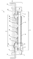
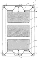
図1は、第1の実施の形態の半導体装置を示す断面図である。
半導体装置1は、樹脂ケース10と、樹脂ケース10に収納された絶縁基板20と、絶縁基板20に配置された半導体素子30とを有する。
FIG. 1 is a cross-sectional view showing the semiconductor device according to the first embodiment.
The semiconductor device 1 includes a
樹脂ケース10は、樹脂で構成され、中央部に矩形型の収納開口部12が下面側に形成され、中央部に矩形型の開口部15が上面側に形成された枠型状の本体部11と、収納開口部12の内周に沿って形成された段差部13と、本体部11に埋設されたリードフレーム14とを備える。
The
絶縁基板20は、セラミック基板21(絶縁板)と、セラミック基板21の上面に形成された第1金属層22と、セラミック基板21の外周縁部に形成された第2金属層23と、セラミック基板21の下面に形成された第3金属層24とを有する。
The
セラミック基板21は、例えば、アルミナ、窒化アルミニウム、窒化シリコン等のセラミックにより構成されている。セラミック基板21の熱伝導率は、100W/(m・k)であって、厚さは、630μm程度である。なお、この厚さは、半導体装置1としてセラミック基板21が熱応力による耐久性を確保するために最低限必要な量である。
The
第1金属層22と第2金属層23と第3金属層24とは、同一の、例えば、銅等の材料により構成されている。また、第1金属層22と第2金属層23と第3金属層24との厚さは、200μm〜400μmであって、第1の実施の形態では、例えば、240μm程度である。
The
半導体素子30は、例えば、IGBT(Insulated Gate Bipolar Transistor)、MOSFET(Metal Oxide Semiconductor Field Effect Transistor)、FWD(Free Wheeling Diode)等である。このような半導体素子30は、絶縁基板20の第1金属層22上にはんだ(図示を省略)により接合されている。
The
半導体装置1は、樹脂ケース10の収納開口部12に、半導体素子30が配置された絶縁基板20が収納され、半導体素子30の電極(図示を省略)とリードフレーム14とがワイヤ25により電気的に接続されている。さらに、半導体装置1は、収納開口部12内の絶縁基板20と半導体素子30とが封止樹脂26により封止されて構成されている。
In the semiconductor device 1, the
次に、半導体装置1に設けられた第2金属層23の絶縁基板20(セラミック基板21)に対する配置について図2を用いて説明する。
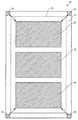
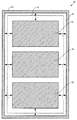
図2は、第1の実施の形態の半導体装置の絶縁基板を示す平面図である。
Next, the arrangement of the
FIG. 2 is a plan view showing an insulating substrate of the semiconductor device according to the first embodiment.
図2では、第1金属層22及び第2金属層23がセラミック基板21の上面に配置された絶縁基板20の平面図を示している。但し、半導体素子30の図示については省略している。また、このような絶縁基板20を樹脂ケース10の収納開口部12に収納させた際の段差部13の位置を破線で示している。
FIG. 2 shows a plan view of the
絶縁基板20は、図2に示されるように、セラミック基板21に第1金属層22が3つ配置されている。第2金属層23は、セラミック基板21の上面の外周縁部における角部にそれぞれ形成されている。また、第2金属層23は、平面視で、絶縁基板20の中心部に対して凸の円弧状(扇型)を成している。このような第1金属層22と第2金属層23とは、例えば、セラミック基板21上に形成した銅箔をエッチングすることにより、同様に、同じ厚さで形成される。
As shown in FIG. 2, the
このようにして形成された第2金属層23は、絶縁基板20の中心部に対して凸の円弧状(扇型)を成していることから、第1金属層22(の角部)から距離r以上が保たれている。
Since the
次に、図1に示す半導体装置1の断面図の要部Aについて図3を用いて説明する。
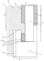
図3は、第1の実施の形態の半導体装置を示す要部断面図である。
収納開口部12に形成された段差部13は、収納開口部12の内周縁に沿って形成された内周面13aと、内周面13aに対して垂直であって、収納開口部12の内周縁に沿って形成された座面13bと、内周面13aに平行で収納開口部12より開口が小さい開口部15の内周縁に沿って形成された内周面13cにより構成されている。半導体装置1では、図3に示されるように、絶縁基板20の第2金属層23の上面は、収納開口部12の段差部13の座面13bに当接している。絶縁基板20の第2金属層23の側面は、収納開口部12の段差部13の内周面13aに当接している。図2に示した段差部13の位置の破線は、内周面13cに相当する。このようにして、絶縁基板20は、収納開口部12の段差部13に嵌められている。
Next, a main part A of the cross-sectional view of the semiconductor device 1 shown in FIG. 1 will be described with reference to FIG.
FIG. 3 is a fragmentary cross-sectional view showing the semiconductor device of the first embodiment.
The
この際、第2金属層23の厚さに応じて、絶縁基板20の第3金属層24の下面が、樹脂ケース10の下面(第1主面)と同一面に揃えられ、または、樹脂ケース10の下面(第1主面)から突出する。なお、図2では、樹脂ケース10の絶縁基板20の収納深さ(内周面13aの高さ(樹脂ケース10の下面から座面13bまでの長さ))が、例えば、1.1mm程度とする。また、絶縁基板20の厚さは、セラミック基板21(630μm)と第2金属層23(240μm)と第3金属層24(240μm)との厚さを合わせた少なくとも1.11mm程度とする。図3では、第3金属層24の下面が、樹脂ケース10の下面から突出している場合を示している。
At this time, according to the thickness of the
このように、上記半導体装置1では、樹脂ケース10の収納開口部12に収納される絶縁基板20は、絶縁板21と、絶縁板21の上面に形成された第1金属層22と、当該上面の外周縁部に形成され、段差部13に当接する第2金属層23と、絶縁板21の下面に形成され、樹脂ケース10の下面と同一面に揃えられ、または、樹脂ケース10の下面から突出する第3金属層24とを有する。
As described above, in the semiconductor device 1, the
第2金属層23は、既述の通り、セラミック基板21上に形成した銅等をエッチングすることにより、第1金属層22と共に、第1金属層22と同じ厚さで形成される。このようにして形成される第2金属層23は、樹脂ケース10の収納深さに合わせて、その厚さを比較的自由に変えることができる。このため、半導体装置1を薄型化することが可能となる。
As described above, the
また、半導体装置1では、セラミック基板21上において、第1金属層22と、セラミック基板21の上面の各角部に形成された第2金属層23との間が封止樹脂26により封止されている。すなわち、第1金属層22と第2金属層23とで構成される凹凸に封止樹脂26が入り込み、当該封止樹脂26が硬化することで、封止樹脂26の樹脂ケース10と絶縁基板20とに対する接着力が高まる(アンカー効果)。このため、第2金属層23を配置することで、封止樹脂26による封止力が向上し、半導体装置1の外部からの衝撃等による信頼性が向上する。
Further, in the semiconductor device 1, a sealing
また、半導体装置1では、第2金属層23をセラミック基板21の各角部に配置し、第2金属層23が平面視で絶縁基板20の中心部に対して凸の円弧状(扇状)を成している。このため、第2金属層23は、第1金属層22から一定の距離が確保されるようになり、第2金属層23と第1金属層22との絶縁性を維持することができるようになる。具体的には、第1金属層22と第3金属層24との間に生じる電位差は、第1金属層22と各第2金属層23との間に封止樹脂26を介して生じる静電容量と、各第2金属層23と第3金属層24との間にセラミック基板21を介して生じる静電容量との比に基づき、第1金属層22と第2金属層23とにそれぞれ印加される。それぞれに印加される電位差が封止樹脂26の絶縁耐圧を超えないように第2金属層23は、第1金属層22に対して距離r以上の間隔が設けられている。
In the semiconductor device 1, the
ここで、第1の実施の形態の半導体装置1に対する参考例として、第1の実施の形態の樹脂ケース10に、半導体素子30が設置された別の基板が収納された半導体装置について、図4を用いて説明する。
Here, as a reference example for the semiconductor device 1 of the first embodiment, a semiconductor device in which another substrate on which the
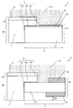
図4は、参考例の半導体装置を示す要部断面図である。
なお、図4(A)は、樹脂ケース10に、金属絶縁基板40を収納させた場合を、図4(B)は、樹脂ケース10に、第2金属層23を除いた絶縁基板20を収納させた場合をそれぞれ示している。また、図4では、半導体素子30の図示を省略している。
FIG. 4 is a cross-sectional view of main parts showing a semiconductor device of a reference example.
4A shows the case where the
図4(A)では、第1の実施の形態の樹脂ケース10の収納開口部12に、金属絶縁基板40が収納されている。
金属絶縁基板40は、アルミニウム等で構成された支持母材41と、支持母材41上に形成された、樹脂材料により構成される絶縁板42と、絶縁板42上に、銅箔等により形成された金属層43とを有する。なお、金属絶縁基板40は絶縁板42で樹脂ケース10の段差部13(座面13b)と当接している。これにより、樹脂ケース10と金属絶縁基板40との絶縁性が保たれる。
In FIG. 4A, the
The
絶縁板42の熱伝導率は、10W/(m・k)程度であり、第1の実施の形態の絶縁基板20(セラミック基板21)の熱伝導率と比べると十分小さい。このため、金属絶縁基板40では、絶縁板42の厚さを100μm程度に薄くして、ある一定の熱伝導率が維持されるようにしている。
The thermal conductivity of the insulating
また、金属絶縁基板40の強度を確保するために、支持母材41の厚さを1mm程度にしている。金属絶縁基板40を樹脂ケース10の収納開口部12に収納させる際には、樹脂ケース10の下面に設置する外部冷却体と金属絶縁基板40との熱抵抗を低減させ、また、安定化させるために、金属絶縁基板40を樹脂ケース10の下面から50μm程度突出させても構わない。樹脂ケース10の金属絶縁基板40の収納深さは、金属絶縁基板40の支持母材41と絶縁板42との厚さを合わせた少なくとも1.1mm程度を要する。
Further, in order to ensure the strength of the
一方、第1の実施の形態では、第1金属層22と第2金属層23とを配置させた絶縁基板20を樹脂ケース10に収納させるようにしている。絶縁基板20では、第2金属層23を配置することにより(図3)、金属絶縁基板40を収納する樹脂ケース10を利用することができる。さらに、絶縁基板20の第3金属層24の下面が、樹脂ケース10の下面と同一面に揃えられ、または、樹脂ケース10の下面から突出する。このため、図4(A)と同様に、樹脂ケース10の下面に配置する外部冷却体と絶縁基板20との熱抵抗を低減させ、また、安定化させることができる。また、絶縁基板20のセラミック基板21の熱伝導率は、100W/(m・K)であり、金属絶縁基板40の絶縁板42よりも大きいために、金属絶縁基板40よりも放熱性が高くなる。
On the other hand, in the first embodiment, the insulating
また、図4(B)に示されるように、樹脂ケース10に、第2金属層23が設けられておらず、第1金属層22を上面に、第3金属層24を下面に有する絶縁基板50を収納させる場合には、絶縁基板50の第3金属層24の下面が、樹脂ケース10の下面に揃わない。このため、絶縁基板50が収納開口部12に収納された樹脂ケース10の収納開口部12に窪みが生じてしまう。このような樹脂ケース10の下面に外部冷却体を設置すると、外部冷却体と、絶縁基板50(第3金属層24)との間に隙間が生じ、放熱性が低下してしまう。
As shown in FIG. 4B, the
そこで、外部冷却体と、絶縁基板50との間の隙間が生じないように、第1金属層22及び第3金属層24を厚くすることが考えられる。しかし、この場合には、第1金属層22及び第3金属層24の熱膨張量が大きくなり、セラミック基板21に対する応力が高くなり信頼性が低下してしまう。また、第1金属層22及び第3金属層24を形成するために、セラミック基板21に形成した銅箔をエッチングすると、銅箔の厚さに比例して、第1金属層22及び第3金属層24の横(セラミック基板21の面)方向へのエッチング量が増加してしまう。このため、隣接する第1金属層22の間隔が広くなり、第1金属層22の面積が小さくなることから、半導体素子30の搭載領域を確保することが難しくなる。さらには、銅箔を厚くすることによる、材料価格と加工工数としてのコストも増加してしまう。
Accordingly, it is conceivable to increase the thickness of the
外部冷却体と、絶縁基板50(第3金属層24)との間に隙間が生じないような別の方法として、セラミック基板21を厚くすることが考えられる。しかし、セラミック基板21を厚くすると、熱伝導率が増加してしまい、放熱性が低下してしまう。
As another method for preventing a gap from being formed between the external cooling body and the insulating substrate 50 (third metal layer 24), it is conceivable to increase the thickness of the
一方、第1の実施の形態では、絶縁基板20(セラミック基板21)の角部に第2金属層23を形成するようにした。これにより、絶縁基板20の第3金属層24の下面が、樹脂ケース10の下面と同一面に揃えられ、または、樹脂ケース10の下面から突出する。このため、樹脂ケース10の下面に外部冷却体を設置しても、絶縁基板20(第3金属層24)と外部冷却体との間に隙間ができないために、放熱性の低下が抑制される。また、絶縁基板20では、図4(B)に対して、セラミック基板21と、第1金属層22と、第3金属層24とを厚くしていない。このため、第1金属層22をエッチングする際に、第1金属層22同士の間隔の広がりを抑制することができ、半導体素子30の搭載領域を確保することができ、また、材料価格と加工工数としてのコストの増加を抑制することができる。セラミック基板21を厚くしていないために、セラミック基板21の熱伝導性の低下を抑制することができ、絶縁基板20の放熱性の低下を防止することができるようになる。
On the other hand, in the first embodiment, the
[第2の実施の形態]
第2の実施の形態では、絶縁基板20に第1の実施の形態と異なる第2金属層が配置されている場合について、図5を用いて説明する。
[Second Embodiment]
In the second embodiment, the case where a second metal layer different from the first embodiment is arranged on the insulating
図5は、第2の実施の形態の半導体装置の絶縁基板を示す平面図である。
第2の実施の形態では、第1の実施の形態(図2)と同様に、セラミック基板21の上面に第1金属層22と、下面に第3金属層24(図示を省略)とがそれぞれ形成されている。
FIG. 5 is a plan view showing an insulating substrate of the semiconductor device according to the second embodiment.
In the second embodiment, as in the first embodiment (FIG. 2), the
また、図5に示されるように、セラミック基板21の上面には、第1金属層22と共に、第2金属層63が形成されている。なお、第1金属層22上に配置される半導体素子30の図示については省略している。また、図5では、このような絶縁基板20を樹脂ケース10(図示を省略)の収納開口部12に収納させた際の段差部13の位置を破線で示している。
Further, as shown in FIG. 5, a
第2の実施の形態の第2金属層63は、図5に示されるように、セラミック基板21の上面の外周縁部に沿って配置されている。また、第2金属層63は、第1金属層22から距離r以上が保たれている。
The
このような第2金属層63が配置された絶縁基板20を、樹脂ケース10の収納開口部12に収納して、セラミック基板21の上面の第1金属層22と、セラミック基板21の上面の外周縁部に形成された第2金属層63との間を封止樹脂26により封止する。すなわち、第1金属層22と第2金属層63とで構成されるセラミック基板21上の凹凸に封止樹脂26が入り込み、当該封止樹脂26が硬化することで、封止樹脂26の樹脂ケース10と絶縁基板20とに対する接着力が高まる。この場合、第2金属層63は、セラミック基板21の外周縁部に沿って設けられているために、第1の実施の形態の場合と比較して、封止樹脂26との接触面積が増える。このため、封止樹脂26による封止力が、第1の実施の形態の場合よりも向上する。
The insulating
また、第2金属層63は、第1金属層22とから一定の距離が確保されるために、第2金属層63と第1金属層22との絶縁性を維持することができるようになる。
[第3の実施の形態]
第3の実施の形態では、第1の実施の形態の絶縁基板20の外周縁部に複数の第2金属層を配置した場合について、図6を用いて説明する。
In addition, since the
[Third Embodiment]
In the third embodiment, a case where a plurality of second metal layers are arranged on the outer peripheral edge portion of the insulating
図6は、第3の実施の形態の半導体装置の絶縁基板を示す平面図である。
第3の実施の形態では、第1の実施の形態(図2)と同様に、セラミック基板21の上面に第1金属層22と、下面に第3金属層24(図示を省略)とがそれぞれ形成されている。
FIG. 6 is a plan view showing an insulating substrate of the semiconductor device of the third embodiment.
In the third embodiment, similarly to the first embodiment (FIG. 2), the
また、図6に示されるように、セラミック基板21の上面には、第1金属層22と共に、第2金属層73,74が形成されている。なお、第1金属層22上に配置される半導体素子30の図示については省略している。また、図6では、このような絶縁基板20を樹脂ケース10の収納開口部12に収納させた際の段差部13の位置を破線で示している。
As shown in FIG. 6, second metal layers 73 and 74 are formed on the upper surface of the
セラミック基板21の上面の外周縁部の角部に、第2金属層73がそれぞれ配置されている。また、セラミック基板21の上面の外周縁部の長手方向の辺に、第2金属層74がそれぞれ配置されている。
Second metal layers 73 are respectively disposed at corners of the outer peripheral edge of the upper surface of the
第3の実施の形態の第2金属層73は、図6に示されるように、平面視で、絶縁基板20の中心部に対して凹の円弧状を成している。このような第2金属層73は、絶縁基板20の中心部に対して凹の円弧状を成していることから、第1金属層22の角部から距離rが保たれている。
As shown in FIG. 6, the
また、第2金属層74は、二等辺三角形状であって、長さの等しい2つの辺が下に凸の円弧状を成している。また、このような第2金属層74は、その頂点が、隣接する第1金属層22の対向する角部からそれぞれ等距離になるように、セラミック基板21の外周縁部の長手方向の辺上に配置されている。第2金属層74は、隣接するそれぞれの第1金属層22の中心部に対して凹の円弧状を成していることから、隣接する第1金属層22の対向する角部からそれぞれ距離rが保たれている。
Further, the
このような第2金属層73,74が配置された絶縁基板20を、樹脂ケース10の収納開口部12に収納して、セラミック基板21の上面の第1金属層22と、セラミック基板21の上面の外周縁部に形成された第2金属層73,74との間を封止樹脂26により封止する。すなわち、第1金属層22と第2金属層73,74とで構成されるセラミック基板21上の凹凸に封止樹脂26が入り込み、当該封止樹脂26が硬化することで、封止樹脂26の樹脂ケース10と絶縁基板20とに対する接着力が高まる。この場合、第1の実施の形態と比べて、第2金属層73に加えて、第2金属層74が、セラミック基板21の外周縁部に設けられているために、封止樹脂26との接触面積が増える。このため、封止樹脂26による封止力が、第1の実施の形態の場合よりも、向上する。
The insulating
また、第2金属層73,74は、第1金属層22から一定の距離rが確保されるために、第2金属層73,74と第1金属層22との絶縁性を維持することができるようになる。
Further, the second metal layers 73 and 74 can maintain the insulation between the second metal layers 73 and 74 and the
[第4の実施の形態]
第4の実施の形態では、第1の実施の形態の絶縁基板20の外周縁部に複数の第2金属層を配置した場合について、図7を用いて説明する。
[Fourth Embodiment]
In the fourth embodiment, a case where a plurality of second metal layers are arranged on the outer peripheral edge portion of the insulating
図7は、第4の実施の形態の半導体装置の絶縁基板を示す平面図である。
第4の実施の形態では、第1の実施の形態(図2)と同様に、セラミック基板21の上面に第1金属層22と、下面に第3金属層24(図示を省略)とがそれぞれ形成されている。
FIG. 7 is a plan view showing an insulating substrate of the semiconductor device of the fourth embodiment.
In the fourth embodiment, as in the first embodiment (FIG. 2), the
また、図7に示されるように、セラミック基板21の上面には、第1金属層22と共に、第2金属層73,75が形成されている。なお、第1金属層22上に配置される半導体素子30の図示については省略している。また、図7では、このような絶縁基板20を樹脂ケース10の収納開口部12に収納させた際の段差部13の位置を破線で示している。
Further, as shown in FIG. 7, second metal layers 73 and 75 are formed on the upper surface of the
セラミック基板21の上面の外周縁部の角部に、第2金属層73がそれぞれ配置されている。また、セラミック基板21の上面の外周縁部の短手方向の辺に、第2金属層75がそれぞれ配置されている。さらに、第2金属層75に対向する第1金属層22の辺に切り欠き部76が形成されている。なお、第1金属層22の切り欠き部76は、第1金属層22において半導体素子30の搭載領域が確保されるように形成される。
Second metal layers 73 are respectively disposed at corners of the outer peripheral edge of the upper surface of the
第4の実施の形態の第2金属層73は、第3の実施の形態と同様に、平面視で、絶縁基板20の中心部に対して凹の円弧状を成している。このような第2金属層73は、下に凸の円弧状を成していることから、第1金属層22の角部から距離rが保たれている。
The
また、第2金属層75は、図7に示されるように、等脚台形状を成して、セラミック基板21の上面の外周縁部の短手方向の辺の中央部に配置されている。また、このような第2金属層75は、第1金属層22の切り欠き部76に対向するように配置されている。このため、第2金属層75は、第1金属層22から距離rが保たれている。
Further, as shown in FIG. 7, the
このような第2金属層73,75が配置された絶縁基板20を、樹脂ケース10の収納開口部12に収納して、セラミック基板21の上面の第1金属層22と、セラミック基板21の上面の外周縁部に形成された第2金属層73,75との間を封止樹脂26により封止する。すなわち、第1金属層22(並びに第1金属層22の切り欠け部76)と第2金属層73,75とで構成されるセラミック基板21上の凹凸に封止樹脂26が入り込み、当該封止樹脂26が硬化することで、封止樹脂26の樹脂ケース10と絶縁基板20とに対する接着力が高まる。この場合、第1の実施の形態と比べて、第2金属層73に加えて、第2金属層75が、セラミック基板21の外周縁部に沿って設けられているために、封止樹脂26との接触面積が増える。このため、封止樹脂26による封止力が、第1の実施の形態の場合よりも、向上する。
The insulating
また、第2金属層73,75は、第1金属層22並びに第1金属層22の切り欠き部76から一定の距離rが確保されるため、第2金属層73,75と第1金属層22との絶縁性を維持することができるようになる。
In addition, since the second metal layers 73 and 75 have a certain distance r from the
なお、図7に示す絶縁基板20のセラミック基板21に、第3の実施の形態の第2金属層74を配置することも可能である。この場合の絶縁基板20を樹脂ケース10の収納開口部12に収納して、第1金属層22と、セラミック基板21の上面の外周縁部に形成された第2金属層73,74,75との間を封止樹脂26により封止する。この場合も、第1の実施の形態と比べて、第2金属層73に加えて、第2金属層74,75が、セラミック基板21の外周縁部に沿って設けられているために、封止樹脂26による封止力が、第1の実施の形態の場合よりも向上する。
It is also possible to dispose the
また、第2金属層73,74,75は、第1金属層22並びに第1金属層22の切り欠き部76から一定の距離rが確保されるようになり、第2金属層73,74,75と第1金属層22との絶縁性を維持することができるようになる。
In addition, the second metal layers 73, 74, 75 are secured at a certain distance r from the
1 半導体装置
10 樹脂ケース
11 本体部
12 収納開口部
13 段差部
14 リードフレーム
15 開口部
20 絶縁基板
21 セラミック基板
22 第1金属層
23 第2金属層
24 第3金属層
25 ワイヤ
26 封止樹脂
30 半導体素子
DESCRIPTION OF SYMBOLS 1
Claims (12)
前記収納開口部に収納され、絶縁板と、前記絶縁板の第2主面に形成された第1金属層と、前記第2主面の外周縁部に形成され、前記段差部に当接する第2金属層と、前記絶縁板の第3主面に形成され、前記第1主面と同一面に揃えられ、または、前記第1主面から突出する第3金属層と、を有する絶縁基板と、
前記第1金属層上に設けられた半導体素子と、
を有する半導体装置。 A case in which a storage opening is formed on the first main surface side, and a step is provided on the inner periphery of the storage opening;
The insulating plate, the first metal layer formed on the second main surface of the insulating plate, and the outer peripheral edge portion of the second main surface, and is in contact with the stepped portion. An insulating substrate having two metal layers and a third metal layer formed on the third main surface of the insulating plate and aligned with the first main surface or protruding from the first main surface; ,
A semiconductor element provided on the first metal layer;
A semiconductor device.
をさらに有する請求項1記載の半導体装置。 The semiconductor device according to claim 1, further comprising: a sealing resin that seals the insulating substrate and the semiconductor element in the storage opening.
請求項1または2記載の半導体装置。 The insulating plate is a ceramic substrate;
The semiconductor device according to claim 1.
請求項1乃至3のいずれかに記載の半導体装置。 The first metal layer has a rectangular shape in plan view, and the second metal layer is disposed on the insulating plate at a predetermined distance or more away from the first metal layer.
The semiconductor device according to claim 1.
請求項4記載の半導体装置。 The second metal layer is formed at each corner of the second main surface,
The semiconductor device according to claim 4.
請求項5記載の半導体装置。 The second metal layer has an arc shape in a plan view, and is separated from the corner portion of the adjacent first metal layer by the distance or more.
The semiconductor device according to claim 5.
請求項6記載の半導体装置。 The second metal layer has a convex or concave arc shape with respect to the center of the insulating substrate in plan view.
The semiconductor device according to claim 6.
請求項4記載の半導体装置。 The second metal layer is formed along an outer peripheral edge of the insulating plate;
The semiconductor device according to claim 4.
請求項4記載の半導体装置。 The second metal layer has an isosceles triangle shape, and is formed in a concave arc shape with respect to the center of the second metal layer in which two sides having the same length are adjacent to each other. The apexes are arranged on the sides of the insulating plate so as to be equidistant from the opposing corners of the adjacent first metal layer, respectively.
The semiconductor device according to claim 4.
前記第1金属層は、前記第2金属層と対向する側に、切り欠き部が形成され、前記第2金属層から前記距離以上離れている、
請求項4記載の半導体装置。 The second metal layer is disposed on a side of the insulating plate facing the first metal layer;
The first metal layer has a notch formed on the side facing the second metal layer, and is separated from the second metal layer by the distance or more.
The semiconductor device according to claim 4.
請求項1乃至10記載の半導体装置。 The first metal layer and the second metal layer are made of the same material.
The semiconductor device according to claim 1.
請求項1乃至11記載の半導体装置。 The first metal layer and the second metal layer have the same height.
The semiconductor device according to claim 1.
Priority Applications (4)
| Application Number | Priority Date | Filing Date | Title |
|---|---|---|---|
| JP2015119372A JP6515694B2 (en) | 2015-06-12 | 2015-06-12 | Semiconductor device |
| CN201610301482.3A CN106252294B (en) | 2015-06-12 | 2016-05-09 | semiconductor device |
| US15/150,556 US9711429B2 (en) | 2015-06-12 | 2016-05-10 | Semiconductor device having a substrate housed in the housing opening portion |
| DE102016208034.2A DE102016208034B4 (en) | 2015-06-12 | 2016-05-10 | semiconductor device |
Applications Claiming Priority (1)
| Application Number | Priority Date | Filing Date | Title |
|---|---|---|---|
| JP2015119372A JP6515694B2 (en) | 2015-06-12 | 2015-06-12 | Semiconductor device |
Publications (2)
| Publication Number | Publication Date |
|---|---|
| JP2017005170A true JP2017005170A (en) | 2017-01-05 |
| JP6515694B2 JP6515694B2 (en) | 2019-05-22 |
Family
ID=57395464
Family Applications (1)
| Application Number | Title | Priority Date | Filing Date |
|---|---|---|---|
| JP2015119372A Active JP6515694B2 (en) | 2015-06-12 | 2015-06-12 | Semiconductor device |
Country Status (4)
| Country | Link |
|---|---|
| US (1) | US9711429B2 (en) |
| JP (1) | JP6515694B2 (en) |
| CN (1) | CN106252294B (en) |
| DE (1) | DE102016208034B4 (en) |
Cited By (2)
| Publication number | Priority date | Publication date | Assignee | Title |
|---|---|---|---|---|
| JP6461441B1 (en) * | 2017-07-03 | 2019-01-30 | 三菱電機株式会社 | Semiconductor device |
| JP2020092223A (en) * | 2018-12-07 | 2020-06-11 | 三菱電機株式会社 | Semiconductor device and power conversion device |
Families Citing this family (10)
| Publication number | Priority date | Publication date | Assignee | Title |
|---|---|---|---|---|
| JPWO2018092318A1 (en) * | 2016-11-21 | 2019-01-24 | オリンパス株式会社 | Endoscopic imaging module and endoscope |
| JPWO2020090411A1 (en) * | 2018-10-30 | 2021-09-16 | 住友電気工業株式会社 | Semiconductor device |
| WO2020121680A1 (en) * | 2018-12-10 | 2020-06-18 | 富士電機株式会社 | Semiconductor device |
| JP7247574B2 (en) * | 2018-12-19 | 2023-03-29 | 富士電機株式会社 | semiconductor equipment |
| CN109659294B (en) * | 2019-01-15 | 2021-10-29 | 江苏双聚智能装备制造有限公司 | A power conversion circuit device |
| JP7351102B2 (en) * | 2019-05-09 | 2023-09-27 | 富士電機株式会社 | Manufacturing method of semiconductor device |
| JP2021132080A (en) * | 2020-02-18 | 2021-09-09 | 富士電機株式会社 | Semiconductor device |
| JP7332528B2 (en) * | 2020-04-17 | 2023-08-23 | 三菱電機株式会社 | Semiconductor device and method for manufacturing semiconductor device |
| CN112331643B (en) * | 2020-10-20 | 2025-07-25 | 广东汇芯半导体有限公司 | Intelligent power module and manufacturing method thereof |
| JP7470074B2 (en) * | 2021-03-10 | 2024-04-17 | 株式会社 日立パワーデバイス | Semiconductor Module |
Citations (3)
| Publication number | Priority date | Publication date | Assignee | Title |
|---|---|---|---|---|
| JPH0487659U (en) * | 1990-11-30 | 1992-07-30 | ||
| JPH06188363A (en) * | 1992-10-21 | 1994-07-08 | Mitsubishi Electric Corp | Semiconductor power module and manufacturing method thereof |
| JP2001127238A (en) * | 1999-10-27 | 2001-05-11 | Mitsubishi Electric Corp | Semiconductor module and insulating substrate for semiconductor module |
Family Cites Families (5)
| Publication number | Priority date | Publication date | Assignee | Title |
|---|---|---|---|---|
| DE4418426B4 (en) * | 1993-09-08 | 2007-08-02 | Mitsubishi Denki K.K. | Semiconductor power module and method of manufacturing the semiconductor power module |
| JP3758383B2 (en) | 1998-10-23 | 2006-03-22 | 富士電機デバイステクノロジー株式会社 | Power semiconductor device and assembly method thereof |
| EP2816598B1 (en) * | 2012-02-13 | 2020-03-18 | Panasonic Intellectual Property Management Co., Ltd. | Semiconductor device and method for manufacturing same |
| JP2013258321A (en) | 2012-06-13 | 2013-12-26 | Fuji Electric Co Ltd | Semiconductor device |
| JP6041053B2 (en) * | 2013-06-10 | 2016-12-07 | 富士電機株式会社 | Semiconductor device and manufacturing method thereof |
-
2015
- 2015-06-12 JP JP2015119372A patent/JP6515694B2/en active Active
-
2016
- 2016-05-09 CN CN201610301482.3A patent/CN106252294B/en active Active
- 2016-05-10 DE DE102016208034.2A patent/DE102016208034B4/en active Active
- 2016-05-10 US US15/150,556 patent/US9711429B2/en active Active
Patent Citations (3)
| Publication number | Priority date | Publication date | Assignee | Title |
|---|---|---|---|---|
| JPH0487659U (en) * | 1990-11-30 | 1992-07-30 | ||
| JPH06188363A (en) * | 1992-10-21 | 1994-07-08 | Mitsubishi Electric Corp | Semiconductor power module and manufacturing method thereof |
| JP2001127238A (en) * | 1999-10-27 | 2001-05-11 | Mitsubishi Electric Corp | Semiconductor module and insulating substrate for semiconductor module |
Cited By (4)
| Publication number | Priority date | Publication date | Assignee | Title |
|---|---|---|---|---|
| JP6461441B1 (en) * | 2017-07-03 | 2019-01-30 | 三菱電機株式会社 | Semiconductor device |
| JP2020092223A (en) * | 2018-12-07 | 2020-06-11 | 三菱電機株式会社 | Semiconductor device and power conversion device |
| JP7045978B2 (en) | 2018-12-07 | 2022-04-01 | 三菱電機株式会社 | Semiconductor devices and power converters |
| US11404340B2 (en) | 2018-12-07 | 2022-08-02 | Mitsubishi Electric Corporation | Semiconductor device and power conversion apparatus |
Also Published As
| Publication number | Publication date |
|---|---|
| US20160365298A1 (en) | 2016-12-15 |
| JP6515694B2 (en) | 2019-05-22 |
| DE102016208034A1 (en) | 2016-12-15 |
| CN106252294B (en) | 2020-05-22 |
| CN106252294A (en) | 2016-12-21 |
| DE102016208034B4 (en) | 2023-09-07 |
| US9711429B2 (en) | 2017-07-18 |
Similar Documents
| Publication | Publication Date | Title |
|---|---|---|
| JP6515694B2 (en) | Semiconductor device | |
| US7847395B2 (en) | Package and package assembly of power device | |
| JP7247574B2 (en) | semiconductor equipment | |
| JP6033522B1 (en) | Insulated circuit board, power module and power unit | |
| JP7006812B2 (en) | Semiconductor device | |
| JP6526229B2 (en) | Power module | |
| JP2014003095A (en) | Semiconductor device | |
| CN103515332A (en) | Semiconductor package | |
| CN107833913B (en) | Semiconductor device with a plurality of semiconductor chips | |
| CN107431067B (en) | Power module | |
| CN106057743A (en) | Power semiconductor module | |
| JP2015122453A (en) | Power module | |
| JP4367376B2 (en) | Power semiconductor device | |
| JP6459843B2 (en) | Semiconductor device | |
| CN115036276A (en) | Semiconductor device with a plurality of semiconductor chips | |
| JP5783865B2 (en) | Semiconductor device | |
| US12512378B2 (en) | Semiconductor module and semiconductor module manufacturing method | |
| JP6617490B2 (en) | Semiconductor device | |
| JP6409879B2 (en) | Packaged power semiconductor and packaged power semiconductor mounting structure | |
| CN103515338A (en) | Semiconductor module | |
| JP5959285B2 (en) | Semiconductor module | |
| JP6771581B2 (en) | Semiconductor modules and semiconductor devices | |
| JP7677562B1 (en) | Semiconductor Device | |
| JP6527777B2 (en) | Semiconductor device and mounting board having the same | |
| CN115881647A (en) | Semiconductor device with a plurality of semiconductor chips |
Legal Events
| Date | Code | Title | Description |
|---|---|---|---|
| A621 | Written request for application examination |
Free format text: JAPANESE INTERMEDIATE CODE: A621 Effective date: 20180314 |
|
| A977 | Report on retrieval |
Free format text: JAPANESE INTERMEDIATE CODE: A971007 Effective date: 20181109 |
|
| A131 | Notification of reasons for refusal |
Free format text: JAPANESE INTERMEDIATE CODE: A131 Effective date: 20181120 |
|
| A521 | Request for written amendment filed |
Free format text: JAPANESE INTERMEDIATE CODE: A523 Effective date: 20190121 |
|
| TRDD | Decision of grant or rejection written | ||
| A01 | Written decision to grant a patent or to grant a registration (utility model) |
Free format text: JAPANESE INTERMEDIATE CODE: A01 Effective date: 20190319 |
|
| A61 | First payment of annual fees (during grant procedure) |
Free format text: JAPANESE INTERMEDIATE CODE: A61 Effective date: 20190401 |
|
| R150 | Certificate of patent or registration of utility model |
Ref document number: 6515694 Country of ref document: JP Free format text: JAPANESE INTERMEDIATE CODE: R150 |
|
| R250 | Receipt of annual fees |
Free format text: JAPANESE INTERMEDIATE CODE: R250 |
|
| R250 | Receipt of annual fees |
Free format text: JAPANESE INTERMEDIATE CODE: R250 |
|
| R250 | Receipt of annual fees |
Free format text: JAPANESE INTERMEDIATE CODE: R250 |
|
| R250 | Receipt of annual fees |
Free format text: JAPANESE INTERMEDIATE CODE: R250 |
|
| R250 | Receipt of annual fees |
Free format text: JAPANESE INTERMEDIATE CODE: R250 |