JP2017005171A - 半導体装置 - Google Patents
半導体装置 Download PDFInfo
- Publication number
- JP2017005171A JP2017005171A JP2015119459A JP2015119459A JP2017005171A JP 2017005171 A JP2017005171 A JP 2017005171A JP 2015119459 A JP2015119459 A JP 2015119459A JP 2015119459 A JP2015119459 A JP 2015119459A JP 2017005171 A JP2017005171 A JP 2017005171A
- Authority
- JP
- Japan
- Prior art keywords
- fin
- semiconductor
- refrigerant
- semiconductor device
- portions
- Prior art date
- Legal status (The legal status is an assumption and is not a legal conclusion. Google has not performed a legal analysis and makes no representation as to the accuracy of the status listed.)
- Granted
Links
Images















Classifications
-
- H—ELECTRICITY
- H10—SEMICONDUCTOR DEVICES; ELECTRIC SOLID-STATE DEVICES NOT OTHERWISE PROVIDED FOR
- H10W—GENERIC PACKAGES, INTERCONNECTIONS, CONNECTORS OR OTHER CONSTRUCTIONAL DETAILS OF DEVICES COVERED BY CLASS H10
- H10W40/00—Arrangements for thermal protection or thermal control
- H10W40/40—Arrangements for thermal protection or thermal control involving heat exchange by flowing fluids
- H10W40/47—Arrangements for thermal protection or thermal control involving heat exchange by flowing fluids by flowing liquids, e.g. forced water cooling
-
- F—MECHANICAL ENGINEERING; LIGHTING; HEATING; WEAPONS; BLASTING
- F28—HEAT EXCHANGE IN GENERAL
- F28F—DETAILS OF HEAT-EXCHANGE AND HEAT-TRANSFER APPARATUS, OF GENERAL APPLICATION
- F28F3/00—Plate-like or laminated elements; Assemblies of plate-like or laminated elements
- F28F3/02—Elements or assemblies thereof with means for increasing heat-transfer area, e.g. with fins, with recesses, with corrugations
- F28F3/022—Elements or assemblies thereof with means for increasing heat-transfer area, e.g. with fins, with recesses, with corrugations the means being wires or pins
-
- H—ELECTRICITY
- H10—SEMICONDUCTOR DEVICES; ELECTRIC SOLID-STATE DEVICES NOT OTHERWISE PROVIDED FOR
- H10W—GENERIC PACKAGES, INTERCONNECTIONS, CONNECTORS OR OTHER CONSTRUCTIONAL DETAILS OF DEVICES COVERED BY CLASS H10
- H10W70/00—Package substrates; Interposers; Redistribution layers [RDL]
- H10W70/01—Manufacture or treatment
- H10W70/02—Manufacture or treatment of conductive package substrates serving as an interconnection, e.g. of metal plates
- H10W70/027—Mechanical treatments, e.g. deforming, punching or cutting
-
- F—MECHANICAL ENGINEERING; LIGHTING; HEATING; WEAPONS; BLASTING
- F28—HEAT EXCHANGE IN GENERAL
- F28F—DETAILS OF HEAT-EXCHANGE AND HEAT-TRANSFER APPARATUS, OF GENERAL APPLICATION
- F28F3/00—Plate-like or laminated elements; Assemblies of plate-like or laminated elements
- F28F3/12—Elements constructed in the shape of a hollow panel, e.g. with channels
-
- H—ELECTRICITY
- H10—SEMICONDUCTOR DEVICES; ELECTRIC SOLID-STATE DEVICES NOT OTHERWISE PROVIDED FOR
- H10W—GENERIC PACKAGES, INTERCONNECTIONS, CONNECTORS OR OTHER CONSTRUCTIONAL DETAILS OF DEVICES COVERED BY CLASS H10
- H10W40/00—Arrangements for thermal protection or thermal control
- H10W40/20—Arrangements for cooling
- H10W40/22—Arrangements for cooling characterised by their shape, e.g. having conical or cylindrical projections
- H10W40/226—Arrangements for cooling characterised by their shape, e.g. having conical or cylindrical projections characterised by projecting parts, e.g. fins to increase surface area
- H10W40/228—Arrangements for cooling characterised by their shape, e.g. having conical or cylindrical projections characterised by projecting parts, e.g. fins to increase surface area the projecting parts being wire-shaped or pin-shaped
-
- H—ELECTRICITY
- H10—SEMICONDUCTOR DEVICES; ELECTRIC SOLID-STATE DEVICES NOT OTHERWISE PROVIDED FOR
- H10W—GENERIC PACKAGES, INTERCONNECTIONS, CONNECTORS OR OTHER CONSTRUCTIONAL DETAILS OF DEVICES COVERED BY CLASS H10
- H10W72/00—Interconnections or connectors in packages
- H10W72/90—Bond pads, in general
- H10W72/921—Structures or relative sizes of bond pads
- H10W72/926—Multiple bond pads having different sizes
Landscapes
- Engineering & Computer Science (AREA)
- Physics & Mathematics (AREA)
- Thermal Sciences (AREA)
- Mechanical Engineering (AREA)
- General Engineering & Computer Science (AREA)
- Cooling Or The Like Of Semiconductors Or Solid State Devices (AREA)
- Cooling Or The Like Of Electrical Apparatus (AREA)
Abstract
Description
これは、熱抵抗の低い半導体モジュールでは、同じ発熱量であってもΔTjが高くなることを示している。しかしながら、熱抵抗が高いと、温度上限から高電流を流せない。このため、所望の出力(例えば100Arms)を流すためには素子を並列接続したり、素子サイズを増加させることが必要となる。これにより、パワー素子を構成するチップ面積の増大ひいてはコスト増大を招く。すなわち、熱抵抗が高いほどコストが増大するという関係を有していることから、放熱効率を高めることで素子発熱温度を低下させ、素子サイズの縮小を図ることが重要となる。
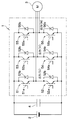
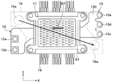
本発明の第1実施形態について説明する。本実施形態では、本発明の一実施形態にかかる半導体モジュールを有する半導体装置の適用例として、例えば三相交流モータなどの駆動を行う三相インバータ回路が備えられた半導体モジュールを有する半導体装置を例に挙げて説明する。
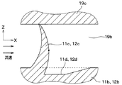
本発明の第2実施形態について説明する。本実施形態は、第1実施形態に対してフィン部11c、12cの形状を変更したものであり、その他については第1実施形態と同様であるため、第1実施形態と異なる部分についてのみ説明する。
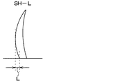
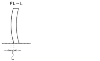
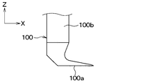
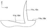
本発明の第3実施形態について説明する。本実施形態は、第2実施形態に対してフィン部11c、12cの形状およびそれを形成するための掘り起こし工具100の刃先100aの形状を変更したものである。その他については第1実施形態と同様であるため、第1実施形態と異なる部分についてのみ説明する。
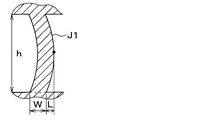
第3実施形態では、フィン部11c、12cのうちの掘り起こした面側を先細り形状とした一例として、フィン部11c、12cの断面形状を楕円弧状の曲面とした。この他の先細り形状、例えば図28に示すように、フィン部11c、12cのうちの掘り起こした面側をV字形状の面としても良い。このようにしても、第3実施形態と同様の効果を得ることができる。このような構造については、図29に示すように、掘り起こし工具100の刃先100aの先端形状をV字形状とすることで加工可能である。
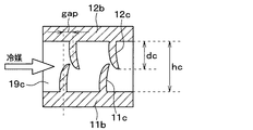
本発明の第4実施形態について説明する。本実施形態は、第1実施形態に対して半導体モジュール6を複数枚積層するものであり、その他については第1実施形態と同様であるため、第1実施形態と異なる部分についてのみ説明する。
本発明は上記した実施形態に限定されるものではなく、特許請求の範囲に記載した範囲内において適宜変更が可能である。
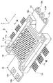
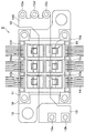
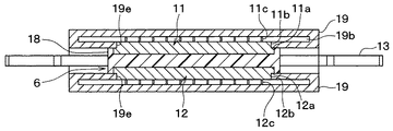
6 半導体モジュール
10 半導体チップ
11、12 上側および下側放熱板
11b、12b 内側部
11c、12c フィン部
11d、12d 凹部
13 多層配線バスバー
18 樹脂モールド部
19 冷却器
Claims (10)
- 発熱素子となる半導体素子(51a〜56a)と、前記半導体素子を覆う板状の樹脂モールド部(18)と、前記樹脂モールド部に封止されると共に、該樹脂モールド部の一面から露出させられ、前記半導体素子と絶縁されつつ、前記半導体素子の発した熱の放熱を行う放熱板(11、12)と、を有する半導体モジュール(6)と、
前記半導体モジュールにおける前記放熱板が露出させられている一面に配置され、冷媒通路(19b)を構成し、該冷媒通路内に冷媒が流されることで前記放熱板からの放熱を促進させる冷却器(19)と、を備え、
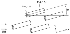
前記放熱板には、該放熱板の表面を掘り起こして形成されたフィン部(11c、12c)が備えられ、該フィン部は先細り形状とされると共に根元部から先端部に至るまで湾曲した楕円弧状とされていることを特徴とする半導体装置。 - 前記フィン部の掘り起こし方向と前記冷媒が流れる方向である冷媒流れ方向とが鋭角をなしていることを特徴とする請求項1に記載の半導体装置。
- 楕円弧状とされた前記フィン部の凸面側が前記冷媒流れの上流側に向けられ、凹面側が前記冷媒流れの下流側に向けられていることを特徴とする請求項2に記載の半導体装置。
- 楕円弧状とされた前記フィン部の凹面側が前記冷媒流れの上流側に向けられ、凸面側が前記冷媒流れの下流側に向けられていることを特徴とする請求項2に記載の半導体装置。
- 前記フィン部よりも下流に、該フィン部を掘り起こして形成された凹部(11d、12d)が位置していることを特徴とする請求項2ないし4のいずれか1つに記載の半導体装置。
- 前記フィン部の掘り起こし方向と前記冷媒流れ方向とのなす角度が0°より大きく45°以下の鋭角であることを特徴とする請求項2ないし5のいずれか1つに記載の半導体装置。
- 前記放熱板は、該放熱板における外縁部(11a、12a)と、該外縁部よりも内側となる内側部(11b、12b)とを有して構成され、前記内側部が前記外縁部から突き出していると共に該内側部の表面を掘り起こすことで前記フィン部が形成されており、
前記冷却器は、前記冷媒通路を構成する中空板状部(19c)を有し、該中空板状部に、前記冷媒通路に繋がると共に前記内側部および前記フィン部が挿入される開口部(19e)が形成され、該中空板状部における前記開口部が形成された一面の厚みが前記内側部の前記外縁部からの突き出し量とされていることを特徴とする請求項2ないし6のいずれか1つに記載の半導体装置。 - 前記フィン部の高さよりも、前記冷媒通路における前記フィン部の高さ方向の寸法の方が小さくされていることを特徴とする請求項7に記載の半導体装置。
- 前記冷却部を挟んで2つの前記半導体モジュールが配置され、
前記冷却部における前記中空板状部のうち2つの前記半導体モジュールが配置される面それぞれに、2つの前記半導体モジュールに備えられた前記放熱板の前記フィン部および前記内側部が挿入される前記開口部が備えられており、
2つの前記半導体モジュールそれぞれの前記フィン部の高さの合計よりも、該フィン部の高さ方向における前記冷媒通路の寸法が小さくされ、
2つの前記半導体モジュールそれぞれの前記内側部の表面方向において、2つの前記半導体モジュールそれぞれの前記フィン部の形成位置がずらされていることを特徴とする請求項7に記載の半導体装置。 - 前記フィン部における前記掘り起こし側の面の断面形状が先細り形状とされていることを特徴とする請求項1ないし9のいずれか1つに記載の半導体装置。
Priority Applications (3)
| Application Number | Priority Date | Filing Date | Title |
|---|---|---|---|
| JP2015119459A JP6503909B2 (ja) | 2015-06-12 | 2015-06-12 | 半導体装置 |
| PCT/JP2016/002357 WO2016199352A1 (ja) | 2015-06-12 | 2016-05-13 | 半導体装置 |
| EP16807069.6A EP3309827B1 (en) | 2015-06-12 | 2016-05-13 | Semiconductor device |
Applications Claiming Priority (1)
| Application Number | Priority Date | Filing Date | Title |
|---|---|---|---|
| JP2015119459A JP6503909B2 (ja) | 2015-06-12 | 2015-06-12 | 半導体装置 |
Publications (2)
| Publication Number | Publication Date |
|---|---|
| JP2017005171A true JP2017005171A (ja) | 2017-01-05 |
| JP6503909B2 JP6503909B2 (ja) | 2019-04-24 |
Family
ID=57503758
Family Applications (1)
| Application Number | Title | Priority Date | Filing Date |
|---|---|---|---|
| JP2015119459A Active JP6503909B2 (ja) | 2015-06-12 | 2015-06-12 | 半導体装置 |
Country Status (3)
| Country | Link |
|---|---|
| EP (1) | EP3309827B1 (ja) |
| JP (1) | JP6503909B2 (ja) |
| WO (1) | WO2016199352A1 (ja) |
Cited By (6)
| Publication number | Priority date | Publication date | Assignee | Title |
|---|---|---|---|---|
| JP2020017587A (ja) * | 2018-07-24 | 2020-01-30 | 株式会社豊田自動織機 | 冷却器 |
| JP2020038935A (ja) * | 2018-09-05 | 2020-03-12 | 株式会社デンソー | 半導体装置 |
| US11075144B2 (en) | 2018-08-09 | 2021-07-27 | Fuji Electric Co., Ltd. | Cooler and semiconductor module |
| JP2022170647A (ja) * | 2021-04-28 | 2022-11-10 | 日本電産株式会社 | 放熱部材及び冷却装置 |
| JP2022187107A (ja) * | 2021-06-07 | 2022-12-19 | 富士電機株式会社 | 冷却器、半導体装置及び電力変換装置 |
| JP2024163691A (ja) * | 2023-05-12 | 2024-11-22 | 矢崎総業株式会社 | 放熱構造 |
Families Citing this family (2)
| Publication number | Priority date | Publication date | Assignee | Title |
|---|---|---|---|---|
| JP7243262B2 (ja) * | 2019-02-15 | 2023-03-22 | 富士電機株式会社 | 半導体モジュール、車両および製造方法 |
| DE102019133871B4 (de) * | 2019-12-11 | 2024-03-14 | Semikron Elektronik Gmbh & Co. Kg | Kondensatoranordnung mit einem Kondensator und mit einer Flüssigkeitskühleinrichtung |
Citations (5)
| Publication number | Priority date | Publication date | Assignee | Title |
|---|---|---|---|---|
| JPS6296854U (ja) * | 1985-12-05 | 1987-06-20 | ||
| JPH0745762A (ja) * | 1993-07-30 | 1995-02-14 | Fujitsu Ltd | 半導体素子冷却装置 |
| JP2005142247A (ja) * | 2003-11-05 | 2005-06-02 | Nakamura Mfg Co Ltd | 放熱器およびその製造方法 |
| JP2007208154A (ja) * | 2006-02-06 | 2007-08-16 | Hitachi Ltd | 電子機器用の冷却装置 |
| US20110079376A1 (en) * | 2009-10-03 | 2011-04-07 | Wolverine Tube, Inc. | Cold plate with pins |
Family Cites Families (3)
| Publication number | Priority date | Publication date | Assignee | Title |
|---|---|---|---|---|
| JP4596235B2 (ja) * | 2004-03-15 | 2010-12-08 | 中村製作所株式会社 | 金属材への微細溝の形成方法 |
| JP4826887B2 (ja) * | 2005-10-28 | 2011-11-30 | 中村製作所株式会社 | 液冷熱交換器を備えた電子部品用パッケージ、およびその形成方法 |
| JP5582364B2 (ja) * | 2012-02-01 | 2014-09-03 | 株式会社デンソー | 突起形成装置、突起形成方法および熱交換器 |
-
2015
- 2015-06-12 JP JP2015119459A patent/JP6503909B2/ja active Active
-
2016
- 2016-05-13 WO PCT/JP2016/002357 patent/WO2016199352A1/ja not_active Ceased
- 2016-05-13 EP EP16807069.6A patent/EP3309827B1/en active Active
Patent Citations (5)
| Publication number | Priority date | Publication date | Assignee | Title |
|---|---|---|---|---|
| JPS6296854U (ja) * | 1985-12-05 | 1987-06-20 | ||
| JPH0745762A (ja) * | 1993-07-30 | 1995-02-14 | Fujitsu Ltd | 半導体素子冷却装置 |
| JP2005142247A (ja) * | 2003-11-05 | 2005-06-02 | Nakamura Mfg Co Ltd | 放熱器およびその製造方法 |
| JP2007208154A (ja) * | 2006-02-06 | 2007-08-16 | Hitachi Ltd | 電子機器用の冷却装置 |
| US20110079376A1 (en) * | 2009-10-03 | 2011-04-07 | Wolverine Tube, Inc. | Cold plate with pins |
Cited By (10)
| Publication number | Priority date | Publication date | Assignee | Title |
|---|---|---|---|---|
| JP2020017587A (ja) * | 2018-07-24 | 2020-01-30 | 株式会社豊田自動織機 | 冷却器 |
| JP7035878B2 (ja) | 2018-07-24 | 2022-03-15 | 株式会社豊田自動織機 | 冷却器 |
| US11075144B2 (en) | 2018-08-09 | 2021-07-27 | Fuji Electric Co., Ltd. | Cooler and semiconductor module |
| JP2020038935A (ja) * | 2018-09-05 | 2020-03-12 | 株式会社デンソー | 半導体装置 |
| CN110880484A (zh) * | 2018-09-05 | 2020-03-13 | 株式会社电装 | 半导体装置 |
| JP7087850B2 (ja) | 2018-09-05 | 2022-06-21 | 株式会社デンソー | 半導体装置 |
| CN110880484B (zh) * | 2018-09-05 | 2024-05-24 | 株式会社电装 | 半导体装置 |
| JP2022170647A (ja) * | 2021-04-28 | 2022-11-10 | 日本電産株式会社 | 放熱部材及び冷却装置 |
| JP2022187107A (ja) * | 2021-06-07 | 2022-12-19 | 富士電機株式会社 | 冷却器、半導体装置及び電力変換装置 |
| JP2024163691A (ja) * | 2023-05-12 | 2024-11-22 | 矢崎総業株式会社 | 放熱構造 |
Also Published As
| Publication number | Publication date |
|---|---|
| JP6503909B2 (ja) | 2019-04-24 |
| WO2016199352A1 (ja) | 2016-12-15 |
| EP3309827A4 (en) | 2018-07-11 |
| EP3309827A1 (en) | 2018-04-18 |
| EP3309827B1 (en) | 2020-08-05 |
Similar Documents
| Publication | Publication Date | Title |
|---|---|---|
| JP6503909B2 (ja) | 半導体装置 | |
| CN101622707B (zh) | 半导体模块及逆变器装置 | |
| JP5434986B2 (ja) | 半導体モジュールおよびそれを備えた半導体装置 | |
| US7859103B2 (en) | Semiconductor module and inverter device | |
| CN101622708B (zh) | 半导体模块及逆变器装置 | |
| US11456233B2 (en) | Semiconductor module, vehicle and manufacturing method | |
| JP5893369B2 (ja) | 半導体装置 | |
| JP7187992B2 (ja) | 半導体モジュールおよび車両 | |
| US9721875B2 (en) | Power module and fabrication method for the same | |
| CN111554645B (zh) | 集成叠层母排的双面水冷SiC半桥模块封装结构 | |
| CN104412383A (zh) | 半导体装置以及半导体装置的连接构造 | |
| US20150137344A1 (en) | Semiconductor device and method for manufacturing same | |
| JP5481104B2 (ja) | 半導体装置 | |
| CN114695322A (zh) | 功率模组 | |
| JP7237647B2 (ja) | 回路基板および電子装置 | |
| JP4532303B2 (ja) | 半導体モジュール | |
| JP2011211017A (ja) | 半導体モジュールおよびそれを備えた半導体装置 | |
| CN115425007A (zh) | 一种芯片连接件及功率模块 | |
| US20240057303A1 (en) | Semiconductor cooling arrangement with improved heatsink | |
| WO2008001413A1 (en) | Power converter | |
| JP2024011697A (ja) | 半導体装置 | |
| CN114664767A (zh) | 具有改进挡板的半导体冷却装置 | |
| CN224006613U (zh) | 功率模块和功率转换系统 | |
| CN210052740U (zh) | 一种低电感高均流的igbt模块 | |
| JP2025043103A (ja) | 半導体モジュール |
Legal Events
| Date | Code | Title | Description |
|---|---|---|---|
| A621 | Written request for application examination |
Free format text: JAPANESE INTERMEDIATE CODE: A621 Effective date: 20170727 |
|
| A131 | Notification of reasons for refusal |
Free format text: JAPANESE INTERMEDIATE CODE: A131 Effective date: 20180320 |
|
| A521 | Request for written amendment filed |
Free format text: JAPANESE INTERMEDIATE CODE: A523 Effective date: 20180518 |
|
| A131 | Notification of reasons for refusal |
Free format text: JAPANESE INTERMEDIATE CODE: A131 Effective date: 20181009 |
|
| A521 | Request for written amendment filed |
Free format text: JAPANESE INTERMEDIATE CODE: A523 Effective date: 20181127 |
|
| TRDD | Decision of grant or rejection written | ||
| A01 | Written decision to grant a patent or to grant a registration (utility model) |
Free format text: JAPANESE INTERMEDIATE CODE: A01 Effective date: 20190226 |
|
| A61 | First payment of annual fees (during grant procedure) |
Free format text: JAPANESE INTERMEDIATE CODE: A61 Effective date: 20190311 |
|
| R151 | Written notification of patent or utility model registration |
Ref document number: 6503909 Country of ref document: JP Free format text: JAPANESE INTERMEDIATE CODE: R151 |
|
| R250 | Receipt of annual fees |
Free format text: JAPANESE INTERMEDIATE CODE: R250 |
|
| R250 | Receipt of annual fees |
Free format text: JAPANESE INTERMEDIATE CODE: R250 |
|
| R250 | Receipt of annual fees |
Free format text: JAPANESE INTERMEDIATE CODE: R250 |
|
| R250 | Receipt of annual fees |
Free format text: JAPANESE INTERMEDIATE CODE: R250 |
|
| R250 | Receipt of annual fees |
Free format text: JAPANESE INTERMEDIATE CODE: R250 |