JP2017005196A - Solid-state imaging device and method for manufacturing solid-state imaging device, photoelectric conversion device, imaging device, electronic device, and photoelectric conversion device. - Google Patents
Solid-state imaging device and method for manufacturing solid-state imaging device, photoelectric conversion device, imaging device, electronic device, and photoelectric conversion device. Download PDFInfo
- Publication number
- JP2017005196A JP2017005196A JP2015120303A JP2015120303A JP2017005196A JP 2017005196 A JP2017005196 A JP 2017005196A JP 2015120303 A JP2015120303 A JP 2015120303A JP 2015120303 A JP2015120303 A JP 2015120303A JP 2017005196 A JP2017005196 A JP 2017005196A
- Authority
- JP
- Japan
- Prior art keywords
- photoelectric conversion
- layer
- transport layer
- conversion layer
- hole transport
- Prior art date
- Legal status (The legal status is an assumption and is not a legal conclusion. Google has not performed a legal analysis and makes no representation as to the accuracy of the status listed.)
- Granted
Links
Images




Classifications
-
- H—ELECTRICITY
- H10—SEMICONDUCTOR DEVICES; ELECTRIC SOLID-STATE DEVICES NOT OTHERWISE PROVIDED FOR
- H10F—INORGANIC SEMICONDUCTOR DEVICES SENSITIVE TO INFRARED RADIATION, LIGHT, ELECTROMAGNETIC RADIATION OF SHORTER WAVELENGTH OR CORPUSCULAR RADIATION
- H10F39/00—Integrated devices, or assemblies of multiple devices, comprising at least one element covered by group H10F30/00, e.g. radiation detectors comprising photodiode arrays
- H10F39/10—Integrated devices
- H10F39/12—Image sensors
- H10F39/18—Complementary metal-oxide-semiconductor [CMOS] image sensors; Photodiode array image sensors
- H10F39/182—Colour image sensors
-
- H—ELECTRICITY
- H10—SEMICONDUCTOR DEVICES; ELECTRIC SOLID-STATE DEVICES NOT OTHERWISE PROVIDED FOR
- H10F—INORGANIC SEMICONDUCTOR DEVICES SENSITIVE TO INFRARED RADIATION, LIGHT, ELECTROMAGNETIC RADIATION OF SHORTER WAVELENGTH OR CORPUSCULAR RADIATION
- H10F39/00—Integrated devices, or assemblies of multiple devices, comprising at least one element covered by group H10F30/00, e.g. radiation detectors comprising photodiode arrays
- H10F39/10—Integrated devices
- H10F39/12—Image sensors
- H10F39/191—Photoconductor image sensors
- H10F39/192—Colour image sensors
-
- H—ELECTRICITY
- H10—SEMICONDUCTOR DEVICES; ELECTRIC SOLID-STATE DEVICES NOT OTHERWISE PROVIDED FOR
- H10K—ORGANIC ELECTRIC SOLID-STATE DEVICES
- H10K30/00—Organic devices sensitive to infrared radiation, light, electromagnetic radiation of shorter wavelength or corpuscular radiation
- H10K30/10—Organic devices sensitive to infrared radiation, light, electromagnetic radiation of shorter wavelength or corpuscular radiation comprising heterojunctions between organic semiconductors and inorganic semiconductors
-
- H—ELECTRICITY
- H10—SEMICONDUCTOR DEVICES; ELECTRIC SOLID-STATE DEVICES NOT OTHERWISE PROVIDED FOR
- H10K—ORGANIC ELECTRIC SOLID-STATE DEVICES
- H10K85/00—Organic materials used in the body or electrodes of devices covered by this subclass
- H10K85/50—Organic perovskites; Hybrid organic-inorganic perovskites [HOIP], e.g. CH3NH3PbI3
-
- H—ELECTRICITY
- H10—SEMICONDUCTOR DEVICES; ELECTRIC SOLID-STATE DEVICES NOT OTHERWISE PROVIDED FOR
- H10K—ORGANIC ELECTRIC SOLID-STATE DEVICES
- H10K39/00—Integrated devices, or assemblies of multiple devices, comprising at least one organic radiation-sensitive element covered by group H10K30/00
- H10K39/30—Devices controlled by radiation
- H10K39/32—Organic image sensors
-
- Y—GENERAL TAGGING OF NEW TECHNOLOGICAL DEVELOPMENTS; GENERAL TAGGING OF CROSS-SECTIONAL TECHNOLOGIES SPANNING OVER SEVERAL SECTIONS OF THE IPC; TECHNICAL SUBJECTS COVERED BY FORMER USPC CROSS-REFERENCE ART COLLECTIONS [XRACs] AND DIGESTS
- Y02—TECHNOLOGIES OR APPLICATIONS FOR MITIGATION OR ADAPTATION AGAINST CLIMATE CHANGE
- Y02E—REDUCTION OF GREENHOUSE GAS [GHG] EMISSIONS, RELATED TO ENERGY GENERATION, TRANSMISSION OR DISTRIBUTION
- Y02E10/00—Energy generation through renewable energy sources
- Y02E10/50—Photovoltaic [PV] energy
- Y02E10/549—Organic PV cells
-
- Y—GENERAL TAGGING OF NEW TECHNOLOGICAL DEVELOPMENTS; GENERAL TAGGING OF CROSS-SECTIONAL TECHNOLOGIES SPANNING OVER SEVERAL SECTIONS OF THE IPC; TECHNICAL SUBJECTS COVERED BY FORMER USPC CROSS-REFERENCE ART COLLECTIONS [XRACs] AND DIGESTS
- Y02—TECHNOLOGIES OR APPLICATIONS FOR MITIGATION OR ADAPTATION AGAINST CLIMATE CHANGE
- Y02P—CLIMATE CHANGE MITIGATION TECHNOLOGIES IN THE PRODUCTION OR PROCESSING OF GOODS
- Y02P70/00—Climate change mitigation technologies in the production process for final industrial or consumer products
- Y02P70/50—Manufacturing or production processes characterised by the final manufactured product
Landscapes
- Chemical & Material Sciences (AREA)
- Engineering & Computer Science (AREA)
- Materials Engineering (AREA)
- Inorganic Chemistry (AREA)
- Physics & Mathematics (AREA)
- Electromagnetism (AREA)
- Solid State Image Pick-Up Elements (AREA)
- Light Receiving Elements (AREA)
- Electroluminescent Light Sources (AREA)
- Transforming Light Signals Into Electric Signals (AREA)
Abstract
【課題】特定の波長の光に対して高い分光特性で、かつ、高い光電変換効率で適切に光電変換する。
【解決手段】入射光を光電変換する光電変換層、光電変換層に対して正孔を輸送する正孔輸送層、および光電変換層に対して電子を輸送する電子輸送層とが一対の電極の間に積層され、光電変換層を、特定の波長領域のみの光を選択的に吸収する層状有機ペロブスカイト材料により構成する。本技術は、固体撮像素子に適用することができる。
【選択図】図6Proper photoelectric conversion is performed with high spectral characteristics and high photoelectric conversion efficiency for light of a specific wavelength.
A photoelectric conversion layer that photoelectrically converts incident light, a hole transport layer that transports holes to the photoelectric conversion layer, and an electron transport layer that transports electrons to the photoelectric conversion layer are a pair of electrodes. The photoelectric conversion layer, which is laminated between them, is composed of a layered organic perovskite material that selectively absorbs light only in a specific wavelength region. The present technology can be applied to a solid-state imaging device.
[Selection] Figure 6
Description
本技術は、固体撮像素子および固体撮像素子の製造方法、光電変換素子、撮像装置、電子機器、並びに光電変換素子に関し、特に、特定の波長の光による光電変換を実現できるようにした固体撮像素子および固体撮像素子の製造方法、光電変換素子、撮像装置、電子機器、並びに光電変換素子に関する。 The present technology relates to a solid-state imaging device, a method for manufacturing the solid-state imaging device, a photoelectric conversion device, an imaging apparatus, an electronic device, and a photoelectric conversion device, and in particular, a solid-state imaging device that can realize photoelectric conversion using light of a specific wavelength. The present invention relates to a method for manufacturing a solid-state imaging element, a photoelectric conversion element, an imaging apparatus, an electronic device, and a photoelectric conversion element.
縦分光型固体撮像素子と呼ばれる、高い色再現性を求められる縦分光イメージャが待望されている。この縦分光イメージャを実現するには、高い光電変換特性だけでなく、高い選択分光性が必要である。 There is a need for a vertical spectral imager called a vertical spectral solid-state imaging device that requires high color reproducibility. In order to realize this vertical spectral imager, not only high photoelectric conversion characteristics but also high selective spectral properties are required.
縦分光型固体撮像素子としては、シリコン(Si)材料を用いたものが知られている。 As the vertical spectroscopic solid-state imaging device, one using a silicon (Si) material is known.
ところが、シリコン材料を用いた縦分光型固体撮像素子では、光吸収係数が小さいために、膜厚を厚くせざるを得ず、その結果、画素面積の極小化に伴い、クロスリーク等により、分光特性に限界があった。 However, in a vertical spectral solid-state imaging device using a silicon material, since the light absorption coefficient is small, it is necessary to increase the film thickness. There was a limit to the characteristics.
そこで、近年、有機材料によって形成された光電変換膜が積層された多層構造を有する縦分光型固体撮像素子が提案されている。 Therefore, in recent years, a vertical spectroscopic solid-state imaging device having a multilayer structure in which photoelectric conversion films formed of organic materials are stacked has been proposed.
例えば、青色光、緑色光および赤色光をそれぞれ吸収する有機光電変換膜が順次積層された固体撮像素子が開示されている(特許文献1参照)。特許文献1に開示された固体撮像素子では、それぞれの有機光電変換膜において各色に対応する光が光電変換されることによりそれぞれの色の信号が取り出されている。
For example, a solid-state imaging device in which organic photoelectric conversion films that respectively absorb blue light, green light, and red light are sequentially stacked is disclosed (see Patent Document 1). In the solid-state imaging device disclosed in
また、緑色光を吸収する有機光電変換膜と、シリコンフォトダイオードとが順次積層された固体撮像素子が開示されている(特許文献2参照)。特許文献2に開示された固体撮像素子では、有機光電変換膜にて緑色光の信号が取り出され、シリコンフォトダイオードにて光進入深さの差を用いて分離された青色光および赤色光の信号が取り出されている。
In addition, a solid-state imaging device in which an organic photoelectric conversion film that absorbs green light and a silicon photodiode are sequentially stacked is disclosed (see Patent Document 2). In the solid-state imaging device disclosed in
さらに、有機材料-無機材料のハイブリッド材料である3D型有機ペロブスカイト材料を用いた太陽電池向け光電変換素子が、高い光電変換効率を示す光電変換素子として知られている(非特許文献1参照)。 Furthermore, a photoelectric conversion element for a solar cell using a 3D organic perovskite material that is a hybrid material of an organic material and an inorganic material is known as a photoelectric conversion element exhibiting high photoelectric conversion efficiency (see Non-Patent Document 1).
しかしながら、上述した特許文献1,2のいずれの有機光電変換膜においても、各色の光を十分に選択分光した上で光電変換することができない。
However, in any of the organic photoelectric conversion films of
また、非特許文献1の技術で用いられる3D型有機ペロブスカイト材料は、可視光領域全体を吸収してしまう上、その長波長側の吸収が、緩やかであり、波長の急峻性も低い為、選択的に分光することが難しいので、有効に選択分光した上で、光電変換することができなかった。
In addition, the 3D type organic perovskite material used in the technology of Non-Patent
また、このような理由から、カラーフィルタを付ける方法も考えられるが、コスト高になる。また縦分光素子として用いる必要があることから、カラーフィルタを用いてしまうと、必要な分光特性の感度が取れなくなってしまうため、本質的にカラーフィルタを用いることができない。 For this reason, a method of attaching a color filter can be considered, but the cost becomes high. Moreover, since it is necessary to use it as a vertical spectroscopic element, if a color filter is used, the sensitivity of a required spectral characteristic cannot be obtained, so that the color filter cannot be used essentially.
本技術は、このような状況に鑑みてなされたものであり、特に、特定の波長の光に対して高い選択性で、かつ、高い光電変換効率で光電変換できるようにするものである。 The present technology has been made in view of such a situation, and in particular, enables photoelectric conversion with high selectivity to light of a specific wavelength and high photoelectric conversion efficiency.
本技術の一側面の固体撮像素子は、入射光を光電変換する光電変換層と、前記光電変換層に対して正孔を輸送する正孔輸送層と、前記光電変換層に対して電子を輸送する電子輸送層と、一対の電極とを含み、前記光電変換層、前記正孔輸送層、および前記電子輸送層は、前記一対の電極の間に積層され、前記光電変換層は、特定の波長領域のみの光を選択的に吸収する層状有機ペロブスカイト材料からなる。 A solid-state imaging device according to one aspect of the present technology includes a photoelectric conversion layer that photoelectrically converts incident light, a hole transport layer that transports holes to the photoelectric conversion layer, and an electron that transports electrons to the photoelectric conversion layer. An electron transport layer and a pair of electrodes, wherein the photoelectric conversion layer, the hole transport layer, and the electron transport layer are stacked between the pair of electrodes, and the photoelectric conversion layer has a specific wavelength It consists of a layered organic perovskite material that selectively absorbs light only in the region.
前記層状有機ペロブスカイト材料は、(RNH3)n-Metal-X(2+n)とすることができ、前記Rは、一級アミンを持つ芳香族または複素環化合物のうちの少なくとも1種類以上とすることができ、前記Metalは、Pb、Sn、およびMnのうちの少なくとも1種類以上を含む金属とすることができ、前記Xは、F、Cl、Br、およびIのうちの少なくとも1種類以上を含むハロゲンとすることができ、前記nは、自然数とすることができる。 The layered organic perovskite material may be (RNH3) n-Metal-X (2 + n), and R is at least one of aromatic or heterocyclic compounds having a primary amine. The metal may be a metal including at least one of Pb, Sn, and Mn, and the X includes at least one of F, Cl, Br, and I. Halogen may be used, and n may be a natural number.
前記Rの構造により、前記層状有機ペロブスカイト材料において選択的に吸収される、特定の波長領域の光の、吸収波長最大ピーク、および吸収波長の分布形状を制御させるようにすることができる。 With the structure of R, it is possible to control the absorption wavelength maximum peak and the absorption wavelength distribution shape of light in a specific wavelength region that is selectively absorbed in the layered organic perovskite material.
前記電子輸送層には、TiO2、NiO、WO3、およびTA2O5のいずれかを含ませるようにすることができる。 The electron transport layer may contain any one of TiO2, NiO, WO3, and TA2O5.
前記正孔輸送層には、Spiro-OMeTAD、TiO2、ZnO、およびSnO2のいずれかを含ませるようにすることができる。 The hole transport layer may contain any of Spiro-OMeTAD, TiO2, ZnO, and SnO2.
本技術の一側面の固体撮像素子の製造方法は、第1の電極を形成する第1の工程と、前記第1の電極の上層に、前記光電変換層に対して電子を輸送する電子輸送層を形成する第2の工程と、前記電子輸送層の上層に、特定の波長領域のみの光を選択的に吸収する層状有機ペロブスカイト材料からなる前記光電変換層を形成する第3の工程と、前記光電変換層の上層に、入射光を光電変換する光電変換層に対して正孔を輸送する正孔輸送層を形成する第4の工程と、前記正孔輸送層の上層に、第2の電極を形成する第5の工程とを含む。 A method of manufacturing a solid-state imaging device according to one aspect of the present technology includes: a first step of forming a first electrode; and an electron transport layer that transports electrons to the photoelectric conversion layer on an upper layer of the first electrode. A third step of forming the photoelectric conversion layer made of a layered organic perovskite material that selectively absorbs light only in a specific wavelength region, on the upper layer of the electron transport layer, and A fourth step of forming a hole transport layer for transporting holes to the photoelectric conversion layer for photoelectric conversion of incident light on the photoelectric conversion layer; and a second electrode on the hole transport layer. Forming a fifth step.
本技術の一側面の光電変換素子は、入射光を光電変換する光電変換層と、前記光電変換層に対して正孔を輸送する正孔輸送層と、前記光電変換層に対して電子を輸送する電子輸送層と、一対の電極とを含み、前記光電変換層、前記正孔輸送層、および前記電子輸送層は、前記一対の電極の間に積層され、前記光電変換層は、特定の波長領域のみの光を選択的に吸収する層状有機ペロブスカイト材料からなる。 The photoelectric conversion element according to one aspect of the present technology includes a photoelectric conversion layer that photoelectrically converts incident light, a hole transport layer that transports holes to the photoelectric conversion layer, and an electron that transports electrons to the photoelectric conversion layer. An electron transport layer and a pair of electrodes, wherein the photoelectric conversion layer, the hole transport layer, and the electron transport layer are stacked between the pair of electrodes, and the photoelectric conversion layer has a specific wavelength It consists of a layered organic perovskite material that selectively absorbs light only in the region.
本技術の一側面の撮像装置は、入射光を光電変換する光電変換層と、前記光電変換層に対して正孔を輸送する正孔輸送層と、前記光電変換層に対して電子を輸送する電子輸送層と、一対の電極とを含み、前記光電変換層、前記正孔輸送層、および前記電子輸送層は、前記一対の電極の間に積層され、前記光電変換層は、特定の波長領域のみの光を選択的に吸収する層状有機ペロブスカイト材料からなる。 An imaging device according to an aspect of the present technology includes a photoelectric conversion layer that photoelectrically converts incident light, a hole transport layer that transports holes to the photoelectric conversion layer, and an electron that transports electrons to the photoelectric conversion layer. An electron transport layer and a pair of electrodes, wherein the photoelectric conversion layer, the hole transport layer, and the electron transport layer are stacked between the pair of electrodes, and the photoelectric conversion layer has a specific wavelength region It consists of a layered organic perovskite material that selectively absorbs only light.
本技術の一側面の電子機器は、入射光を光電変換する光電変換層と、前記光電変換層に対して正孔を輸送する正孔輸送層と、前記光電変換層に対して電子を輸送する電子輸送層と、一対の電極とを含み、前記光電変換層、前記正孔輸送層、および前記電子輸送層は、前記一対の電極の間に積層され、前記光電変換層は、特定の波長領域のみの光を選択的に吸収する層状有機ペロブスカイト材料からなる。 An electronic device according to one aspect of the present technology includes a photoelectric conversion layer that photoelectrically converts incident light, a hole transport layer that transports holes to the photoelectric conversion layer, and an electron that transports electrons to the photoelectric conversion layer. An electron transport layer and a pair of electrodes, wherein the photoelectric conversion layer, the hole transport layer, and the electron transport layer are stacked between the pair of electrodes, and the photoelectric conversion layer has a specific wavelength region It consists of a layered organic perovskite material that selectively absorbs only light.
本技術の一側面の光電変換素子は、入射光を光電変換する光電変換層と、前記光電変換層に対して正孔を輸送する正孔輸送層と、前記光電変換層に対して電子を輸送する電子輸送層と、一対の電極とを含み、前記光電変換層、前記正孔輸送層、および前記電子輸送層は、前記一対の電極の間に積層され、前記光電変換層は、特定の波長領域のみの光を選択的に吸収する層状有機ペロブスカイト材料からなる。 The photoelectric conversion element according to one aspect of the present technology includes a photoelectric conversion layer that photoelectrically converts incident light, a hole transport layer that transports holes to the photoelectric conversion layer, and an electron that transports electrons to the photoelectric conversion layer. An electron transport layer and a pair of electrodes, wherein the photoelectric conversion layer, the hole transport layer, and the electron transport layer are stacked between the pair of electrodes, and the photoelectric conversion layer has a specific wavelength It consists of a layered organic perovskite material that selectively absorbs light only in the region.
本技術の一側面においては、光電変換層により、入射光が光電変換され、正孔輸送層により、前記光電変換層に対して正孔が輸送され、電子輸送層により、前記光電変換層に対して電子が輸送され、一対の電極の間に、前記光電変換層、前記正孔輸送層、および前記電子輸送層が、積層され、前記光電変換層が、特定の波長領域のみの光を選択的に吸収する層状有機ペロブスカイト材料により形成される。 In one aspect of the present technology, incident light is photoelectrically converted by the photoelectric conversion layer, holes are transported to the photoelectric conversion layer by the hole transport layer, and to the photoelectric conversion layer by the electron transport layer. Electrons are transported, and the photoelectric conversion layer, the hole transport layer, and the electron transport layer are stacked between a pair of electrodes, and the photoelectric conversion layer selectively selects light only in a specific wavelength region. It is formed of a layered organic perovskite material that absorbs in water.
本技術の一側面によれば、特定の波長の光に対して高い分光特性で、かつ、高い光電変換効率で適切に光電変換することが可能となる。 According to one aspect of the present technology, it is possible to appropriately photoelectrically convert light having a specific wavelength with high spectral characteristics and high photoelectric conversion efficiency.
<本技術を適用した固体撮像素子の実施の形態の構成例>
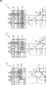
図1は、本技術を適用した光電変換膜を用いた縦分光型の固体撮像素子の一実施の形態の構成例を示した図である。
<Configuration example of embodiment of solid-state imaging device to which the present technology is applied>
FIG. 1 is a diagram illustrating a configuration example of an embodiment of a vertical spectral solid-state imaging device using a photoelectric conversion film to which the present technology is applied.
光電変換膜を用いた縦分光型の固体撮像素子の構成例は、図1の左から示される第1乃至第3の固体撮像素子11からなる3種類の構成とされる。3種類のいずれの構成においても図1中の上部となる光源から図中の下部に向かって光電変換膜およびフォトダイオードのいずれかからなる光電変換素子が積層された構造とされる。
The configuration example of the vertical spectroscopic solid-state imaging device using the photoelectric conversion film has three types of configurations including the first to third solid-
より詳細には、第1の固体撮像素子11は、図1の左上部で示されるように、最上層にG(緑)色の光を光電変換する光電変換膜よりなる光電変換素子21が設けられ、その下に、上から、B(青)色、およびR(赤)色のシリコン製のフォトダイオードからなる光電変換素子31,32が積層されている。
More specifically, as shown in the upper left part of FIG. 1, the first solid-
このような構成により、図1の左下部で示されるように、光電変換素子21によりG(緑)色(一点鎖線)の波長帯の光により光電変換がなされ、その後、順次、波長帯が短い順に光電変換素子31,32によりB(青)色(破線)、およびR(赤)色(実線)の光により光電変換がなされることで、RGB(赤色、緑色、青色)が縦方向に分光されて光電変換される。
With such a configuration, as shown in the lower left part of FIG. 1, photoelectric conversion is performed by light in the G (green) color (dashed line) wavelength band by the
また、第2の固体撮像素子11は、図1の中央上部で示されるように、最上層から順にB(青)色およびG(緑)色の光を光電変換する光電変換膜よりなる光電変換素子22,21が設けられ、その下に、R(赤)色のシリコン製のフォトダイオードからなる光電変換素子32が積層されている。
Further, as shown in the upper center portion of FIG. 1, the second solid-
このような構成により、図1の中央下部で示されるように、光電変換素子22,21により順次波長帯が短い順に、B(青)色およびG(緑)色の波長帯の光により光電変換がなされ、その後、光電変換素子32によりR(赤)色の光により光電変換がなされることで、RGB(赤色、緑色、青色)が縦方向に分光されて光電変換される。
With such a configuration, as shown in the lower center of FIG. 1, photoelectric conversion is performed by light in the B (blue) and G (green) wavelength bands in order of decreasing wavelength band by the
さらに、第3の固体撮像素子11は、図1の右上部で示されるように、最上層から順にB(青)色、G(緑)色、およR(赤)色の光を光電変換する光電変換膜よりなる光電変換素子22,21,23が積層されている。
Further, as shown in the upper right part of FIG. 1, the third solid-
このような構成により、図1の中央下部で示されるように、光電変換素子22,21,23により順次波長帯が短い順に、B(青)色、G(緑)色、R(赤)色の波長帯の光により光電変換がなされることで、RGB(赤色、緑色、青色)が縦方向に分光されて画素信号が生成される。
With such a configuration, as shown in the lower center of FIG. 1, B (blue) color, G (green) color, and R (red) color in order of decreasing wavelength band by
ここで、光電変換膜より構成される光電変換素子21乃至23は、層状(2D:2 Dimension)有機ペロブスカイト材料の薄膜より構成されている。
Here, the
層状有機ペロブスカイト材料とは、有機-無機ぺロブスカイト型化合物の一つの材料群であり、例えば、有機-無機層状ペロブスカイト型化合物(RNH3)2-Metal-X4で記載される。有機層(RNH3+)と無機半導体層(PbX64-)が交互に積層した構造の自己組織的な構造を持つ。Rがメチル等の小さい官能基である場合、3D型構造を取り、ブロードな吸収スペクトルを持つようになる。 The layered organic perovskite material is one material group of organic-inorganic perovskite type compounds and is described, for example, as organic-inorganic layered perovskite type compound (RNH3) 2-Metal-X4. It has a self-organized structure in which organic layers (RNH3 +) and inorganic semiconductor layers (PbX64-) are alternately stacked. When R is a small functional group such as methyl, it takes a 3D type structure and has a broad absorption spectrum.
しかしながら、Rが、例えば、フェニル基以上の大きな官能基を持つと、3D構造ではなく、層状の2D構造を持つようになる。2D構造になると、特定の波長において急峻な分光特性を持つようになることが知られている。 However, when R has a functional group larger than, for example, a phenyl group, it has a layered 2D structure instead of a 3D structure. It is known that a 2D structure has a steep spectral characteristic at a specific wavelength.
光電変換素子21乃至23において使用される光電変換膜を構成する層状有機ペロブスカイト材料は、以下の一般式(1)で表される材料とされる。
The layered organic perovskite material constituting the photoelectric conversion film used in the
(RNH3)n-Metal-X(2n)
一般式(1)
(RNH3) n-Metal-X (2n)
General formula (1)
ここで、一般式(1)において、Rは、一級アミンを持つ芳香族または複素環化合物のうちの少なくとも1種類以上である。また、Metalは、Pb、Sn、およびMnの少なくと1種類以上を含む金属である。さらに、Xは、F、Cl、Br、およびIより少なくとも1種類以上を含むハロゲンである。また、nは、自然数である。 Here, in the general formula (1), R is at least one of aromatic or heterocyclic compounds having a primary amine. Metal is a metal containing at least one of Pb, Sn, and Mn. Furthermore, X is a halogen containing at least one kind from F, Cl, Br, and I. N is a natural number.
層状有機ペロブスカイト材料は、以下のように合成する。すなわち、まず、以下の反応式(1)で示されるように、フェネチルアミン(MA)と、ヨウ化水素(HI)と反応させて、フェネチルアミンのヨウ化水素塩(MAH+I-)を合成する。次に、以下の反応式(2)で示されるように、ジメチルホルムアミドの有機溶媒に、ハロゲン化アミンであるフェネチルアミンのヨウ化水素塩(MAH+I-)と、ヨウ化鉛(PbI2)とを2:1で溶解させ、層状有機ペロブスカイト((MAH)2PbI4)が溶解したインクを作成する。 The layered organic perovskite material is synthesized as follows. That is, first, as shown in the following reaction formula (1), phenethylamine (MA) is reacted with hydrogen iodide (HI) to synthesize a phenethylamine hydrogen iodide salt (MAH + I − ). Next, as shown in the following reaction formula (2), in a dimethylformamide organic solvent, phenethylamine hydroiodide salt (MAH + I − ) and lead iodide (PbI2) are added to a halogenated amine. An ink having a layered organic perovskite ((MAH) 2PbI4) dissolved therein is prepared by dissolution at a ratio of 2: 1.

さらに、層状有機ペロブスカイトを溶解させたインクが、洗浄したガラスに、スピンコートされることにより層状有機ペロブスカイト材料が光電変換層として形成される。ここで、コート条件は、例えば、回転数が2000rpmであり、回転時間が60sであり、この条件において、作成された層状有機ペロブスカイト材料の膜厚は、200nm程度となる。 Furthermore, the layered organic perovskite material is formed as a photoelectric conversion layer by spin-coating the ink, in which the layered organic perovskite is dissolved, onto the washed glass. Here, the coating conditions are, for example, a rotational speed of 2000 rpm and a rotational time of 60 s. Under these conditions, the film thickness of the layered organic perovskite material produced is about 200 nm.
このようにして生成された層状有機ペロブスカイト材料は、例えば、SEM(Scanning Electron Microscope:走査型電子顕微鏡)により観察すると、図2で示されるように良好な平坦性が示される。 When the layered organic perovskite material thus produced is observed with, for example, an SEM (Scanning Electron Microscope), good flatness is shown as shown in FIG.
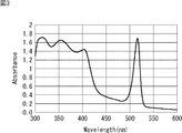
また、紫外可視分光評価装置を用いて、層状有機ペロブスカイト材料の分光特性を測定すると、例えば、図3で示されるように522nmn付近で吸収率がピークとなる。図3で示されるように、吸収率がピークとなる522nmについて、厚みあたりの光吸収係数αは約80000であり、高い吸収係数を持つことが確認されており、分光特性の観点から、例えば、G(緑)色の光電変換素子21に好適な材質であることが示されている。
Further, when the spectral characteristics of the layered organic perovskite material are measured using an ultraviolet-visible spectroscopic evaluation apparatus, for example, as shown in FIG. 3, the absorption peaked in the vicinity of 522 nm. As shown in FIG. 3, the light absorption coefficient α per thickness is about 80,000 for 522 nm where the absorption rate is a peak, and it has been confirmed that the absorption coefficient has a high absorption coefficient. It is shown that the material is suitable for the G (green) color
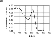
さらに、IPCE(Incident Photon to Current Conversion Efficiency)スペクトル装置を用いて、波長に対する外部量子効率を取得すると、図4で示されるように、522nm付近において、光電変換効率(=外部量子効率EQE)が、約30%になることが示され、良好な光電変換効率が得られることが示される。この結果、層状有機ペロブスカイト材料は、光電変換効率の観点からも、G(緑)色の光電変換素子21に好適な材質であることが示されている。
Furthermore, when the external quantum efficiency with respect to the wavelength is obtained using an IPCE (Incident Photon to Current Conversion Efficiency) spectrum apparatus, as shown in FIG. 4, the photoelectric conversion efficiency (= external quantum efficiency EQE) is around 522 nm, as shown in FIG. It is shown to be about 30%, indicating that good photoelectric conversion efficiency can be obtained. As a result, the layered organic perovskite material is shown to be a suitable material for the G (green)
尚、図4は、固体撮像素子11における光電変換素子21の負バイアス-0.2V IPCEの光電変換特性を示している。図4のIPCEの光電変換特性は、図3の層状有機ペロブスカイト材料の分光特性を反映したものであり、500乃至520nmの可視光が選択的に光電変換されていることを示している。
FIG. 4 shows the photoelectric conversion characteristic of the negative bias −0.2 V IPCE of the
このような特徴を持つ層状有機ペロブスカイト材料を用いた光電変換素子が、例えば、図1に左上部で示される縦分光型の第1の固体撮像素子11の最上部の光電変換素子21として設けられると、500乃至520nmの波長の光のみを選択的に吸収し、450乃至500nm及び540nm以上の光は透過させることになるので、好適なG(緑)色の光電変換素子として機能する。
A photoelectric conversion element using a layered organic perovskite material having such characteristics is provided as, for example, the uppermost
同様に、図1の中央上部の第2の固体撮像素子11、または、右上部の第3の固体撮像素子11で示されるように、光電変換素子21は、縦分光型の固体撮像素子を形成する他の光電変換素子22,32の間、または、22,23の間に挿入することも可能となる。
Similarly, as shown by the second solid-
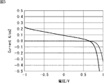
また、層状有機ペロブスカイト材料に対する電圧-電流特性について、暗電流と明電流とを測定したところ、図5で示されるような結果が得られた。すなわち、図5で示されるように、遮光した状態における暗電流については良好なダイオード特性を示し、光を照射した状態における明電流については、電流が増大していることが示されており、光電変換素子として機能していることが示されている。 Further, when the dark current and the bright current were measured with respect to the voltage-current characteristics for the layered organic perovskite material, the results shown in FIG. 5 were obtained. That is, as shown in FIG. 5, the dark current in the light-shielded state shows good diode characteristics, and the bright current in the light-irradiated state shows an increase in current. It is shown that it functions as a conversion element.
尚、図5は、固体撮像素子11における光電変換素子21の負バイアス-0.2V IPCEの暗電流と明電流の電圧-電流特性を示しており、点線が暗電流であり、実線が明電流を表している。
FIG. 5 shows the voltage-current characteristics of the negative bias-0.2 V IPCE dark current and the bright current of the
<層状有機ペロブスカイト材料を用いた光電変換素子の構成例>
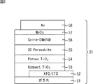
次に、図6を参照して、層状有機ペロブスカイト材料を用いた光電変換素子21乃至23の構成例について説明する。尚、ここでは、光電変換素子21乃至23のうち、代表してG(緑)色の光を選択的に光電変換する光電変換素子21について説明するが、光電変換素子22,23についても同様である。
<Configuration example of photoelectric conversion element using layered organic perovskite material>
Next, a configuration example of the
図中の最下層にガラス層51が設けられており、その上部に透明導電材料であるATO(アンチモンドープ酸化錫)/ITO(酸化インジウム錫)からなる電極層52が形成されている。
A
電極層52の上には、電子輸送層として、Compact TiO2層53が形成されている。尚、Compact TiO2層53は、電子輸送層が形成されれば他の材質からなる層でもよく、例えば、NiO、WO3、またはTA2O5により形成される層でもよい。
On the
Compact TiO2層53の上には、ポーラスTiO2層54が形成されている。ポーラス(Porous)TiO2層54の上には、光電変換素子層となる2D Perovskite(層状有機ペロブスカイト材質)層55が形成されている。2D Perovskite層55の上には、正孔輸送層となるSpiro-OMeTAD層56が形成されている。ここで、Spiro-OMeTADは、以下の化学式(1)で表される化合物1である。
A
Spiro-OMeTAD層56は、正孔輸送層が形成できれば他の材質からなる層でもよく、例えば、TiO2、ZnO、またはSnO2により形成される層でもよい。Spiro-OMeTAD層56の上には、MoOx層57が形成されており、さらに、その上には、Au層58が形成されている。
The Spiro-
<層状有機ペロブスカイト材料を用いた光電変換素子の製造方法>
次に、図7のフローチャートを参照して、層状有機ペロブスカイト材料を用いた光電変換素子の製造方法について説明する。
<Method for Producing Photoelectric Conversion Element Using Layered Organic Perovskite Material>
Next, a method for manufacturing a photoelectric conversion element using a layered organic perovskite material will be described with reference to the flowchart of FIG.
ステップS11において、ITO/ATO層52およびガラス層51が積層された材質25mmの片側5mmの幅で、エッチングが行われ、ITO/ATO層52が部分的に除去される。さらに、ガラス層51が超音波洗浄され(中性洗剤洗浄され、蒸留水洗浄され、イソプロピルアルコール洗浄され、アセトン洗浄され、蒸留水洗浄され)、さらに、UVオゾン処理前処理が行われる。
In step S11, etching is performed with a width of 5 mm on one side of the material 25 mm on which the ITO /
ステップS12において、上述のITO/ATO層52が積層された側に、Tiイソプロポキシドを溶解させたエタノール溶液(2.5%)が、スプレー法が用いられて、塗布され、その後、電気炉において、500℃で、かつ、20分間加熱され、電子輸送層となるCompact TiO2層53が形成される。Compact TiO2層53の膜厚は、例えば、30nm程度である。
In step S12, an ethanol solution (2.5%) in which Ti isopropoxide is dissolved is applied to the side on which the above-described ITO /
より詳細には、電子輸送層は、例えば、多孔質電子輸送材料からなる層とすることが好ましい。多孔質電子輸送材料としては、例えば、TiO2、WO3、ZnO、Nb2O5、Ta2O5、SrTiO3、また、有機電子輸送材料等の一種又は二種以上を採用できる。なお、無機半導体を使用する場合には、ドナーがドープされていてもよい。さらに、有機の電子輸送材料を用いる場合、電子輸送層の厚さは、10乃至2000nm程度が好ましく、20乃至1500nm程度がより好ましい。電子輸送層の厚さを上記範囲内とすることにより、より確実にリーク電流を抑制し、且つ、光吸収層からの電子を収集することができる。 More specifically, the electron transport layer is preferably a layer made of, for example, a porous electron transport material. As the porous electron transport material, for example, one or more of TiO2, WO3, ZnO, Nb2O5, Ta2O5, SrTiO3, and organic electron transport materials can be employed. In addition, when using an inorganic semiconductor, the donor may be doped. Furthermore, when an organic electron transport material is used, the thickness of the electron transport layer is preferably about 10 to 2000 nm, and more preferably about 20 to 1500 nm. By setting the thickness of the electron transport layer within the above range, it is possible to more reliably suppress the leakage current and collect electrons from the light absorption layer.
ステップS13において、Compact TiO2層53上に、TIO2ペーストがスピンコートされ、その後、500℃で、かつ、20分間加熱され、ポーラスTiO2層54が形成される。ポーラスTiO2層54は、例えば、160nm程度である。
In step S13, a TIO2 paste is spin-coated on the
ステップS14において、ポーラスTiO2層54上に、層状有機ペロブスカイト材料が溶解されたインクがスピンコートされ、その後、100℃で、かつ、5分間加熱され、層状有機ペロブスカイト薄膜からなる2D Perovskite層55が形成される。その後、ステップS11の処理で、エッチングされた部分の2D Perovskite層55が、ふき取り除去される。
In step S14, an ink in which a layered organic perovskite material is dissolved is spin-coated on the
ステップS15において、2D Perovskite層55上に、クロロベンゼン1.82ml、Spiro-OMeTAD 14.7mg、Li-TFSI 17mg、および4-tert-ブチルピリジン49mgが混合されたインクが、スピンコート塗布されることにより、正孔輸送層となるSpiro-OMeTAD層56が形成される。
In step S15, an ink mixed with 1.82 ml of chlorobenzene, 14.7 mg of Spiro-OMeTAD, 17 mg of Li-TFSI, and 49 mg of 4-tert-butylpyridine is spin-coated on the 2D Perovskite layer 55, so that A Spiro-
ステップS16において、Spiro-OMeTAD層56上に、真空蒸着機により、MoOx層57およびAu層58が蒸着成膜されて形成される。ここで、MoOx層57の膜厚は、例えば、30nm程度であり、Au層58の膜厚は、例えば、100nm程度の厚みで蒸着成膜される。
In step S <b> 16, the
すなわち、本技術の固体撮像素子に適用される光電変換膜においては、光吸収層の片側に正孔輸送層が設けられている。正孔輸送層に使用される材料としては、spiro-MeO-TADの他に、例えば、セレン、ヨウ化銅(CuI)等のヨウ化物、層状コバルト酸化物等のコバルト錯体、CuSCN、MoO3、NiO、WO3、有機ホール輸送材等が挙げられる。 That is, in the photoelectric conversion film applied to the solid-state imaging device of the present technology, the hole transport layer is provided on one side of the light absorption layer. In addition to spiro-MeO-TAD, materials used for the hole transport layer include, for example, iodides such as selenium and copper iodide (CuI), cobalt complexes such as layered cobalt oxide, CuSCN, MoO3, NiO , WO3, organic hole transport material and the like.
より詳細には、ヨウ化物としては、例えば、ヨウ化銅(CuI)等が挙げられる。層状コバルト酸化物としては、例えば、AxCoO2(A=Li、Na、K、Ca、Sr、Ba;0≦x≦1)等が挙げられる。また、有機ホール輸送材としては、例えば、ポリ−3−ヘキシルチオフェン(P3HT)、ポリエチレンジオキシチオフェン(PEDOT)等のポリチオフェン誘導体、2,2’,7,7’−テトラキス−(N,N−ジ−p−メトキシフェニルアミン)−9,9’−スピロビフルオレン(spiro-MeO-TAD)等のフルオレン誘導体、ポリビニルカルバゾール等のカルバゾール誘導体、トリフェニルアミン誘導体、ジフェニルアミン誘導体、ポリシラン誘導体、ポリアニリン誘導体等が挙げられる。正孔輸送層の厚さは、特に制限されないが、0.01乃至10μm程度が好ましい。 More specifically, examples of the iodide include copper iodide (CuI). Examples of the layered cobalt oxide include AxCoO2 (A = Li, Na, K, Ca, Sr, Ba; 0 ≦ x ≦ 1). Examples of the organic hole transport material include polythiophene derivatives such as poly-3-hexylthiophene (P3HT) and polyethylenedioxythiophene (PEDOT), 2,2 ′, 7,7′-tetrakis- (N, N— Fluorene derivatives such as di-p-methoxyphenylamine) -9,9'-spirobifluorene (spiro-MeO-TAD), carbazole derivatives such as polyvinylcarbazole, triphenylamine derivatives, diphenylamine derivatives, polysilane derivatives, polyaniline derivatives, etc. Is mentioned. The thickness of the hole transport layer is not particularly limited, but is preferably about 0.01 to 10 μm.
また、上記した正孔輸送層は、塗布法だけでなく、メッキ法、スプレー法等の非真空プロセスにより形成することができ、さらに、蒸着プロセスでも形成することが可能である。さらに、正孔輸送層は、電子ブロッキング能力を持つことが望ましい。また正孔輸送層が電子ブロッキング性を持たない場合、もう一層の電子ブロッキング性を有する第2の正孔輸送層を持ち合わせても良い。 The hole transport layer described above can be formed not only by a coating method but also by a non-vacuum process such as a plating method or a spray method, and can also be formed by a vapor deposition process. Furthermore, the hole transport layer desirably has an electron blocking capability. When the hole transport layer does not have an electron blocking property, a second hole transport layer having another electron blocking property may be provided.
さらに、以上においては、Compact TiO2層53、ポーラスTiO2層54、2D Perovskite層55、およびSpiro-OMeTAD層56のいずれの層が形成される際にも、塗布プロセスによる処理である例について説明してきた。しかしながら、これらの層が形成可能な手法であれば、その他の手法でもよく、例えば、蒸着プロセス、転写プロセス、ALD(Atomic Layer Deposition)法、スパッタ法、およびPLD(Pulsed Laser Deposition)法などでもよい。
Furthermore, in the above, an example has been described in which any of the
また、上述した各層の膜厚は一例であり、所定の範囲内であればよいものであり、例えば、Compact TiO2層53の好ましい膜厚の範囲は、2nm乃至100nmの範囲である。また、ポーラスTiO2層54の好ましい膜厚の範囲は、50nm乃至300nmの範囲である。さらに、光電変換層である2D Perovskite層55の好ましい膜厚の範囲は、300nm乃至1000nmの範囲である。また、正孔輸送層であるSpiro-OMeTAD層56の好ましい膜厚の範囲は、50nm乃至300nmの範囲である。
Moreover, the film thickness of each layer mentioned above is an example, and should just be in a predetermined range, for example, the range of the preferable film thickness of the
以上の処理により、特定の波長の光に対して、高い選択性と、高い光電変換特性を有する光電変換膜材料を用いた光電変換素子21を生成することが可能となる。
Through the above processing, it is possible to generate a
<層状有機ペロブスカイト((RNH3)n-Metal-X(2n))材料の特性の制御>
層状有機ペロブスカイト((RNH3)n-Metal-X(2n))材料は、Rである一級アミンを持つ芳香族または複素環化合物のうちの少なくとも1種類以上のものの組み合わせにより吸収波長最大ピーク及び吸収波長の形状を制御することができる。また、同様に、層状有機ペロブスカイト((RNH3)n-Metal-X(2n))材料は、Xである、F、Cl、Br、およびIより少なくとも1種類以上を含むハロゲンの組み合わせにより吸収波長最大ピーク及び吸収波長の形状を制御することができる。
<Control of properties of layered organic perovskite ((RNH3) n-Metal-X (2n))>
The layered organic perovskite ((RNH3) n-Metal-X (2n)) material has a maximum absorption wavelength peak and an absorption wavelength due to a combination of at least one of aromatic or heterocyclic compounds having a primary amine as R. Can be controlled. Similarly, the layered organic perovskite ((RNH3) n-Metal-X (2n)) material has a maximum absorption wavelength due to the combination of X, F, Cl, Br, and a halogen containing at least one kind of I. The shape of the peak and absorption wavelength can be controlled.
Rについては、例えば、以下の化学式(2)乃至化学式(25)で表現される化合物2乃至25のいずれか、または、それらの組み合わせにより層状有機ペロブスカイト((RNH3)n-Metal-X(2n))材料の吸収波長最大ピーク及び吸収波長の分布形状を制御することができる。
従って、この一級アミンを持つ芳香族または複素環化合物であるRおよびハロゲンXの様々な組み合わせにより特性を制御することができるので、例えば、G(緑)色の光を選択的に光電変換する光電変換素子21のみならず、B(青)色、またはR(赤)色の光に対して高い選択性と、高い光電変換特性を備えた光電変換素子22,23を生成することが可能となる。
Therefore, the characteristics can be controlled by various combinations of R and halogen X, which are aromatic or heterocyclic compounds having this primary amine, and, for example, photoelectric conversion that selectively photoelectrically converts G (green) light. It becomes possible to generate not only the
また、図1の第1乃至第3の固体撮像素子11については、光源をRGB(赤色、緑色、青色)の3色からなる固体撮像素子の例を示したものであるが、これ以外の色を用いて配色するようにする場合にでも、対応する色の光(対応する波長の光)を選択的に光電変換する層状有機ペロブスカイト((RNH3)n-Metal-X(2n))材料からなる光電変換膜を生成することで、対応する光を選択的に光電変換する光電変換素子を生成することが可能となる。例えば、光源として、黄色の波長に対応する光を選択的に光電変換する層状有機ペロブスカイト((RNH3)n-Metal-X(2n))材料を生成して、光電変換素子を生成することで、RGB(赤色、緑色、青色)の3色に加えて、Y(黄色)の4色を光源とする画像を撮像することも可能となる。
In addition, the first to third solid-state
<固体撮像素子の構成>
次に、図8および図9を参照して、本技術に係る光電変換素子が適用される固体撮像素子の構成について説明する。図8は、本技術に係る光電変換素子が適用される固体撮像素子の構造を示す概略図である。
<Configuration of solid-state image sensor>
Next, with reference to FIG. 8 and FIG. 9, a configuration of a solid-state imaging element to which the photoelectric conversion element according to the present technology is applied will be described. FIG. 8 is a schematic diagram illustrating a structure of a solid-state imaging element to which the photoelectric conversion element according to the present technology is applied.
ここで、図8において、画素領域201、211、231は、本技術に係る光電変換膜を含む光電変換素子が配置される領域である。また、制御回路202、212、242は、固体撮像素子の各構成を制御する演算処理回路であり、ロジック回路203、223、243は、画素領域において光電変換素子が光電変換した信号を処理するための信号処理回路である。
Here, in FIG. 8,
例えば、図9の構成Aで示されるように、本技術に係る光電変換素子が適用される固体撮像素子は、1つの半導体チップ200内に、画素領域201と、制御回路202と、ロジック回路203とが形成されてもよい。
For example, as illustrated in configuration A in FIG. 9, a solid-state imaging device to which the photoelectric conversion element according to the present technology is applied includes a
また、図9の構成Bで示されるように、本技術に係る光電変換素子が適用される固体撮像素子は、第1半導体チップ210内に、画素領域211と、制御回路212とが形成され、第2半導体チップ220内にロジック回路223が形成された積層型固体撮像素子であってもよい。
9, the solid-state imaging device to which the photoelectric conversion element according to the present technology is applied includes a
さらに、図9の構成Cで示されるように、本技術に係る光電変換素子が適用される固体撮像素子は、第1半導体チップ230内に、画素領域231が形成され、第2半導体チップ240内に制御回路242と、ロジック回路243とが形成された積層型固体撮像素子であってもよい。
Furthermore, as illustrated in the configuration C of FIG. 9, in the solid-state imaging device to which the photoelectric conversion element according to the present technology is applied, the
図9の構成Bおよび構成Cにて示した固体撮像素子は、制御回路およびロジック回路の少なくともいずれか一方が、画素領域が形成された半導体チップとは別の半導体チップ内に形成される。したがって、図9の構成Bおよび構成Cで示した固体撮像素子は、構成Aで示した固体撮像素子よりも画素領域を拡大することができるため、画素領域に搭載される画素を増加させ、平面分解能を向上させることができる。そのため、本技術に係る光電変換素子が適用される固体撮像素子は、図9の構成Bおよび構成Cで示した積層型固体撮像素子であることがより好ましい。 In the solid-state imaging device shown in the configuration B and the configuration C in FIG. 9, at least one of the control circuit and the logic circuit is formed in a semiconductor chip different from the semiconductor chip in which the pixel region is formed. Therefore, since the solid-state imaging device shown in the configuration B and the configuration C in FIG. 9 can expand the pixel region as compared with the solid-state imaging device shown in the configuration A, the number of pixels mounted in the pixel region is increased, and the plane The resolution can be improved. Therefore, the solid-state imaging device to which the photoelectric conversion element according to the present technology is applied is more preferably the stacked solid-state imaging device shown in the configuration B and the configuration C in FIG.
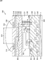
続いて、図9を参照して、本技術に係る光電変換素子が適用された固体撮像素子の具体的な構造について説明する。図9は、本技術に係る光電変換素子が適用された固体撮像素子の単位画素における概略を示した断面図である。なお、図9で示す固体撮像素子300は、画素トランジスタ等が形成された面とは反対側の面から光が入射する裏面照射型の固体撮像素子である。また、図9では、図面に対して上側が受光面となり、下側が画素トランジスタおよび周辺回路が形成される回路形成面となる。
Next, a specific structure of the solid-state imaging device to which the photoelectric conversion device according to the present technology is applied will be described with reference to FIG. FIG. 9 is a cross-sectional view schematically illustrating a unit pixel of a solid-state imaging element to which the photoelectric conversion element according to the present technology is applied. Note that the solid-
図9に示すように、固体撮像素子300は、光電変換領域320において、半導体基板330に形成された第1フォトダイオードPD1を含む光電変換素子、半導体基板330に形成された第2フォトダイオードPD2を含む光電変換素子、および半導体基板330の裏面側に形成された有機光電変換膜310を含む光電変換素子が光の入射方向に積層された構成を有する。
As shown in FIG. 9, the solid-
第1フォトダイオードPD1および、第2フォトダイオードPD2は、シリコンからなる半導体基板330の第1導電型(例えば、p型)半導体領域であるウェル領域331に形成される。
The first photodiode PD1 and the second photodiode PD2 are formed in a
第1フォトダイオードPD1は、半導体基板330の受光面側に形成された第2導電型(例えば、n型)不純物によるn型半導体領域332と、その一部が半導体基板330の表面側に達するように延長して形成された延長部332aとを有する。延長部332aの表面には、電荷蓄積層となる高濃度のp型半導体領域334が形成される。また、延長部332aは、第1フォトダイオードPD1のn型半導体領域332に蓄積された信号電荷を半導体基板330の表面側に抜き出すための抜出層として形成される。
The first photodiode PD1 has an n-
第2フォトダイオードPD2は、半導体基板330の受光面側に形成されたn型半導体領域336と、半導体基板330の表面側に形成され、電荷蓄積層となる高濃度のp型半導体領域338と、にて構成される。
The second photodiode PD2 includes an n-
第1フォトダイオードPD1および第2フォトダイオードPD2において、半導体基板330の界面にp型半導体領域が形成されることにより、半導体基板330界面で発生する暗電流を抑制することができる。
In the first photodiode PD1 and the second photodiode PD2, the dark current generated at the interface of the
ここで、受光面から最も離れた領域に形成された第2フォトダイオードPD2は、例えば、赤色光を吸収し、光電変換する赤色光電変換素子である。また、第2フォトダイオードPD2よりも受光面側に形成された第1フォトダイオードPD1は、例えば、青色光を吸収し、光電変換する青色光電変換素子である。 Here, the second photodiode PD2 formed in the region farthest from the light receiving surface is, for example, a red photoelectric conversion element that absorbs red light and performs photoelectric conversion. The first photodiode PD1 formed on the light receiving surface side of the second photodiode PD2 is, for example, a blue photoelectric conversion element that absorbs blue light and performs photoelectric conversion.
有機光電変換膜310は、反射防止膜302および絶縁膜306を介して半導体基板330の裏面上に形成される。また、有機光電変換膜310は、上部電極312および下部電極308にて挟持されることで光電変換素子を形成する。ここで、有機光電変換膜310は、例えば、緑色光を吸収し、光電変換する有機膜であり、上記で説明した本技術に係る光電変換膜で形成される。また、上部電極312および下部電極308は、例えば、酸化インジウムスズ(ITO)、酸化インジウム亜鉛(IZO)等の透明導電性材料で形成される。
The organic
また、下部電極308は、反射防止膜302を貫通するコンタクトプラグ304を介して、半導体基板330の裏面側から表面側にかけて形成された縦型転送路348に接続される。縦型転送路348は、半導体基板330の裏面側から接続部340、電位障壁層342、電荷蓄積層344、p型半導体領域346の積層構造にて形成される。
The
接続部340は、半導体基板330の裏面側に形成された高不純物濃度のn型不純物領域からなり、コンタクトプラグ304とオーミックコンタクトのために形成される。電位障壁層342は、低濃度のp型不純物領域からなり、接続部340と電荷蓄積層344との間においてポテンシャルバリアを形成する。電荷蓄積層344は、有機光電変換膜310から転送された信号電荷を蓄積し、接続部340よりも低濃度のn型不純物領域で形成される。なお、半導体基板330の表面には、高濃度のp型半導体領域346が形成される。かかるp型半導体領域346により、半導体基板330界面で発生する暗電流が抑制される。
The
ここで、半導体基板330の表面側には、層間絶縁層351を介して複数層に積層された配線358を含む多層配線層350が形成される。また、半導体基板330表面近傍には、第1フォトダイオードPD1、第2フォトダイオードPD2、および有機光電変換膜310に対応する読出回路352、354、356が形成される。読出回路352、354、356は、それぞれの光電変換素子から出力信号を読み出し、ロジック回路(図示せず)に転送する。さらに、多層配線層350の表面には、支持基板360が形成される。
Here, on the surface side of the
一方、上部電極312の受光面側には、第1フォトダイオードPD1の延長部332aおよび縦型転送路348を遮光するように遮光膜316が形成される。ここで、遮光膜316同士によって区切られた領域が光電変換領域320となる。また、遮光膜316上には、平坦化膜314を介してオンチップレンズ318が形成される。
On the other hand, a
以上にて、本技術に係る光電変換素子が適用される固体撮像素子300について説明した。なお、本技術に係る光電変換素子が適用される固体撮像素子300は、単位画素において縦方向に色分離が行われるため、カラーフィルタ等が形成されていない。
The solid-
<電子機器の構成>
続いて、図10を参照して、本技術に係る光電変換素子が適用される電子機器の構成について説明する。図10は、本技術に係る光電変換素子が適用される電子機器の構成を説明するブロック図である。
<Configuration of electronic equipment>
Next, with reference to FIG. 10, a configuration of an electronic apparatus to which the photoelectric conversion element according to the present technology is applied will be described. FIG. 10 is a block diagram illustrating a configuration of an electronic device to which the photoelectric conversion element according to the present technology is applied.
図10に示すように、電子機器400は、光学系402と、固体撮像素子404と、DSP(Digital Signal Processor)回路406と、制御部408と、出力部412と、入力部414と、フレームメモリ416と、記録部418と、電源部420とを備える。
As shown in FIG. 10, the
ここで、DSP回路406、制御部408、出力部412、入力部414、フレームメモリ416、記録部418および電源部420は、バスライン410を介して相互に接続されている。
Here, the
光学系402は、被写体からの入射光を取り込み、固体撮像素子404の撮像面上に結像させる。また、固体撮像素子404は、本技術に係る光電変換素子を含み、光学系402によって撮像面上に結像された入射光の光量を画素単位で電気信号に変換して画素信号として出力する。
The
DSP回路406は、固体撮像素子404から転送された画素信号を処理し、出力部412、フレームメモリ416、および記録部418等に出力する。また、制御部408は、例えば、演算処理回路等で構成され、電子機器400の各構成の動作を制御する。
The
出力部412は、例えば、液晶ディスプレイ、有機エレクトロルミネッセンスディスプレイ等のパネル型表示装置であり、固体撮像素子404にて撮像された動画または静止画を表示する。なお、出力部412は、スピーカおよびヘッドフォン等の音声出力装置を含んでもよい。また、入力部414は、例えば、タッチパネル、ボタン等のユーザが操作を入力するための装置であり、ユーザの操作に従い、電子機器400が有する様々な機能について操作指令を発する。
The
フレームメモリ416は、固体撮像素子404にて撮像された動画または静止画等を一時的に記憶する。また、記録部418は、固体撮像素子404にて撮像された動画または静止画等を磁気ディスク、光ディスク、光磁気ディスク、または半導体メモリ等のリムーバブル記憶媒体に記録する。
The
電源部420は、DSP回路406、制御部408、出力部412、入力部414、フレームメモリ416、および記録部418の動作電源となる各種電源をこれらの供給対象に対して適宜供給する。
The
以上にて、本技術に係る光電変換素子が適用される電子機器400について説明した。本技術に係る光電変換素子が適用される電子機器400は、例えば、撮像装置などであってもよい。
The
また、以上においては、本技術に係る光電変換素子が適用される固体撮像素子、および電子機器について説明してきたが、それ以外の技術にも適用することが可能であり、例えば、太陽電池や光を利用したセンサとして適用することも可能である。 In the above description, the solid-state imaging device and the electronic apparatus to which the photoelectric conversion element according to the present technology is applied have been described. However, the present invention can also be applied to other technologies, such as solar cells and light. It is also possible to apply as a sensor using
以上、添付図面を参照しながら本技術の一実施の形態について詳細に説明したが、本技術にける技術的範囲はかかる例に限定されない。本技術の技術分野における通常の知識を有する者であれば、特許請求の範囲に記載された技術的思想の範疇内において、各種の変更例または修正例に想到し得ることは明らかであり、これらについても、当然に本技術の技術的範囲に属するものと了解される。 Although one embodiment of the present technology has been described in detail with reference to the accompanying drawings, the technical scope of the present technology is not limited to such an example. It is obvious that a person having ordinary knowledge in the technical field of the present technology can come up with various changes or modifications within the scope of the technical idea described in the claims. Of course, it is understood that it belongs to the technical scope of the present technology.
また、本明細書に記載された効果は、あくまで説明的または例示的なものであって限定的ではない。つまり、本技術は、上記の効果とともに、または上記の効果に代えて、本明細書の記載から当業者には明らかな他の効果を奏しうる。 Further, the effects described in the present specification are merely illustrative or exemplary and are not limited. That is, the present technology can exhibit other effects that are apparent to those skilled in the art from the description of the present specification in addition to or instead of the above effects.
尚、本技術は、以下のような構成も取ることができる。
<1> 入射光を光電変換する光電変換層と、
前記光電変換層に対して正孔を輸送する正孔輸送層と、
前記光電変換層に対して電子を輸送する電子輸送層と、
一対の電極とを含み、
前記光電変換層、前記正孔輸送層、および前記電子輸送層は、前記一対の電極の間に積層され、
前記光電変換層は、特定の波長領域のみの光を選択的に吸収する層状有機ペロブスカイト材料からなる
固体撮像素子。
<2> 前記層状有機ペロブスカイト材料は、
(RNH3)n-Metal-X(2+n)
であり、
前記Rは、一級アミンを持つ芳香族または複素環化合物のうちの少なくとも1種類以上であり、
前記Metalは、Pb、Sn、およびMnのうちの少なくとも1種類以上を含む金属であり、
前記Xは、F、Cl、Br、およびIのうちの少なくとも1種類以上を含むハロゲンであり、
前記nは、自然数である
<1>に記載の固体撮像素子。
<3> 前記Rの構造により、前記層状有機ペロブスカイト材料において選択的に吸収される、特定の波長領域の光の、吸収波長最大ピーク、および吸収波長の分布形状が制御される
<2>に記載の固体撮像素子。
<4> 前記電子輸送層は、TiO2、NiO、WO3、およびTA2O5のいずれかを含む
<1>乃至<3>のいずれかに記載の固体撮像素子。
<5> 前記正孔輸送層は、Spiro-OMeTAD、TiO2、ZnO、およびSnO2のいずれかを含む
<1>乃至<4>のいずれかに記載の固体撮像素子。
<6> 第1の電極を形成する第1の工程と、
前記第1の電極の上層に、前記光電変換層に対して電子を輸送する電子輸送層を形成する第2の工程と、
前記電子輸送層の上層に、特定の波長領域のみの光を選択的に吸収する層状有機ペロブスカイト材料からなる前記光電変換層を形成する第3の工程と、
前記光電変換層の上層に、入射光を光電変換する光電変換層に対して正孔を輸送する正孔輸送層を形成する第4の工程と、
前記正孔輸送層の上層に、第2の電極を形成する第5の工程と
を含む固体撮像素子の製造方法。
<7> 入射光を光電変換する光電変換層と、
前記光電変換層に対して正孔を輸送する正孔輸送層と、
前記光電変換層に対して電子を輸送する電子輸送層と、
一対の電極とを含み、
前記光電変換層、前記正孔輸送層、および前記電子輸送層は、前記一対の電極の間に積層され、
前記光電変換層は、特定の波長領域のみの光を選択的に吸収する層状有機ペロブスカイト材料からなる
光電変換素子。
<8> 入射光を光電変換する光電変換層と、
前記光電変換層に対して正孔を輸送する正孔輸送層と、
前記光電変換層に対して電子を輸送する電子輸送層と、
一対の電極とを含み、
前記光電変換層、前記正孔輸送層、および前記電子輸送層は、前記一対の電極の間に積層され、
前記光電変換層は、特定の波長領域のみの光を選択的に吸収する層状有機ペロブスカイト材料からなる
撮像装置。
<9> 入射光を光電変換する光電変換層と、
前記光電変換層に対して正孔を輸送する正孔輸送層と、
前記光電変換層に対して電子を輸送する電子輸送層と、
一対の電極とを含み、
前記光電変換層、前記正孔輸送層、および前記電子輸送層は、前記一対の電極の間に積層され、
前記光電変換層は、特定の波長領域のみの光を選択的に吸収する層状有機ペロブスカイト材料からなる
電子機器。
<10> 入射光を光電変換する光電変換層と、
前記光電変換層に対して正孔を輸送する正孔輸送層と、
前記光電変換層に対して電子を輸送する電子輸送層と、
一対の電極とを含み、
前記光電変換層、前記正孔輸送層、および前記電子輸送層は、前記一対の電極の間に積層され、
前記光電変換層は、特定の波長領域のみの光を選択的に吸収する層状有機ペロブスカイト材料からなる
光電変換素子。
In addition, this technique can also take the following structures.
<1> a photoelectric conversion layer that photoelectrically converts incident light;
A hole transport layer for transporting holes to the photoelectric conversion layer;
An electron transport layer for transporting electrons to the photoelectric conversion layer;
A pair of electrodes,
The photoelectric conversion layer, the hole transport layer, and the electron transport layer are stacked between the pair of electrodes,
The photoelectric conversion layer is made of a layered organic perovskite material that selectively absorbs light only in a specific wavelength region.
<2> The layered organic perovskite material is
(RNH3) n-Metal-X (2 + n)
And
R is at least one of aromatic or heterocyclic compounds having a primary amine,
The Metal is a metal containing at least one of Pb, Sn, and Mn,
X is a halogen containing at least one of F, Cl, Br, and I;
Said n is a natural number. The solid-state image sensor as described in <1>.
<3> The structure of R controls the absorption wavelength maximum peak and the absorption wavelength distribution shape of light in a specific wavelength region that is selectively absorbed in the layered organic perovskite material. Solid-state image sensor.
<4> The solid-state imaging device according to any one of <1> to <3>, wherein the electron transport layer includes any one of TiO2, NiO, WO3, and TA2O5.
<5> The solid-state imaging device according to any one of <1> to <4>, wherein the hole transport layer includes any one of Spiro-OMeTAD, TiO2, ZnO, and SnO2.
<6> a first step of forming a first electrode;
A second step of forming an electron transport layer for transporting electrons to the photoelectric conversion layer on the first electrode;
A third step of forming the photoelectric conversion layer made of a layered organic perovskite material that selectively absorbs light only in a specific wavelength region on the electron transport layer;
A fourth step of forming a hole transport layer that transports holes to the photoelectric conversion layer that photoelectrically converts incident light on the photoelectric conversion layer;
And a fifth step of forming a second electrode on an upper layer of the hole transport layer.
<7> a photoelectric conversion layer that photoelectrically converts incident light;
A hole transport layer for transporting holes to the photoelectric conversion layer;
An electron transport layer for transporting electrons to the photoelectric conversion layer;
A pair of electrodes,
The photoelectric conversion layer, the hole transport layer, and the electron transport layer are stacked between the pair of electrodes,
The photoelectric conversion layer is made of a layered organic perovskite material that selectively absorbs light only in a specific wavelength region.
<8> a photoelectric conversion layer that photoelectrically converts incident light;
A hole transport layer for transporting holes to the photoelectric conversion layer;
An electron transport layer for transporting electrons to the photoelectric conversion layer;
A pair of electrodes,
The photoelectric conversion layer, the hole transport layer, and the electron transport layer are stacked between the pair of electrodes,
The photoelectric conversion layer is an imaging device made of a layered organic perovskite material that selectively absorbs light only in a specific wavelength region.
<9> a photoelectric conversion layer that photoelectrically converts incident light;
A hole transport layer for transporting holes to the photoelectric conversion layer;
An electron transport layer for transporting electrons to the photoelectric conversion layer;
A pair of electrodes,
The photoelectric conversion layer, the hole transport layer, and the electron transport layer are stacked between the pair of electrodes,
The photoelectric conversion layer is an electronic device made of a layered organic perovskite material that selectively absorbs light only in a specific wavelength region.
<10> a photoelectric conversion layer that photoelectrically converts incident light;
A hole transport layer for transporting holes to the photoelectric conversion layer;
An electron transport layer for transporting electrons to the photoelectric conversion layer;
A pair of electrodes,
The photoelectric conversion layer, the hole transport layer, and the electron transport layer are stacked between the pair of electrodes,
The photoelectric conversion layer is made of a layered organic perovskite material that selectively absorbs light only in a specific wavelength region.
11 固体撮像素子, 21乃至23 光電変換素子(光電変換膜), 31,32 光電変換素子(フォトダイオード), 51 ガラス層, 52 電極層, 53 Compact TiO2層, 54 ポーラスTiO2層, 55 2D Perovskite層, 56 Spiro-OMeTAD層, 57 MoOx層, 58 Au層
DESCRIPTION OF
Claims (10)
前記光電変換層に対して正孔を輸送する正孔輸送層と、
前記光電変換層に対して電子を輸送する電子輸送層と、
一対の電極とを含み、
前記光電変換層、前記正孔輸送層、および前記電子輸送層は、前記一対の電極の間に積層され、
前記光電変換層は、特定の波長領域のみの光を選択的に吸収する層状有機ペロブスカイト材料からなる
固体撮像素子。 A photoelectric conversion layer for photoelectrically converting incident light;
A hole transport layer for transporting holes to the photoelectric conversion layer;
An electron transport layer for transporting electrons to the photoelectric conversion layer;
A pair of electrodes,
The photoelectric conversion layer, the hole transport layer, and the electron transport layer are stacked between the pair of electrodes,
The photoelectric conversion layer is made of a layered organic perovskite material that selectively absorbs light only in a specific wavelength region.
(RNH3)n-Metal-X(2+n)
であり、
前記Rは、一級アミンを持つ芳香族または複素環化合物のうちの少なくとも1種類以上であり、
前記Metalは、Pb、Sn、およびMnのうちの少なくとも1種類以上を含む金属であり、
前記Xは、F、Cl、Br、およびIのうちの少なくとも1種類以上を含むハロゲンであり、
前記nは、自然数である
請求項1に記載の固体撮像素子。 The layered organic perovskite material is
(RNH3) n-Metal-X (2 + n)
And
R is at least one of aromatic or heterocyclic compounds having a primary amine,
The Metal is a metal containing at least one of Pb, Sn, and Mn,
X is a halogen containing at least one of F, Cl, Br, and I;
The solid-state imaging device according to claim 1, wherein n is a natural number.
請求項2に記載の固体撮像素子。 The solid-state imaging according to claim 2, wherein the structure of R controls the absorption wavelength maximum peak and the distribution shape of the absorption wavelength of light in a specific wavelength region that is selectively absorbed in the layered organic perovskite material. element.
請求項1に記載の固体撮像素子。 The solid-state imaging device according to claim 1, wherein the electron transport layer includes any one of TiO 2, NiO, WO 3, and TA 2 O 5.
請求項1に記載の固体撮像素子。 The solid-state imaging device according to claim 1, wherein the hole transport layer includes any one of Spiro-OMeTAD, TiO 2, ZnO, and SnO 2.
前記第1の電極の上層に、前記光電変換層に対して電子を輸送する電子輸送層を形成する第2の工程と、
前記電子輸送層の上層に、特定の波長領域のみの光を選択的に吸収する層状有機ペロブスカイト材料からなる前記光電変換層を形成する第3の工程と、
前記光電変換層の上層に、入射光を光電変換する光電変換層に対して正孔を輸送する正孔輸送層を形成する第4の工程と、
前記正孔輸送層の上層に、第2の電極を形成する第5の工程と
を含む固体撮像素子の製造方法。 A first step of forming a first electrode;
A second step of forming an electron transport layer for transporting electrons to the photoelectric conversion layer on the first electrode;
A third step of forming the photoelectric conversion layer made of a layered organic perovskite material that selectively absorbs light only in a specific wavelength region on the electron transport layer;
A fourth step of forming a hole transport layer that transports holes to the photoelectric conversion layer that photoelectrically converts incident light on the photoelectric conversion layer;
And a fifth step of forming a second electrode on an upper layer of the hole transport layer.
前記光電変換層に対して正孔を輸送する正孔輸送層と、
前記光電変換層に対して電子を輸送する電子輸送層と、
一対の電極とを含み、
前記光電変換層、前記正孔輸送層、および前記電子輸送層は、前記一対の電極の間に積層され、
前記光電変換層は、特定の波長領域のみの光を選択的に吸収する層状有機ペロブスカイト材料からなる
光電変換素子。 A photoelectric conversion layer for photoelectrically converting incident light;
A hole transport layer for transporting holes to the photoelectric conversion layer;
An electron transport layer for transporting electrons to the photoelectric conversion layer;
A pair of electrodes,
The photoelectric conversion layer, the hole transport layer, and the electron transport layer are stacked between the pair of electrodes,
The photoelectric conversion layer is made of a layered organic perovskite material that selectively absorbs light only in a specific wavelength region.
前記光電変換層に対して正孔を輸送する正孔輸送層と、
前記光電変換層に対して電子を輸送する電子輸送層と、
一対の電極とを含み、
前記光電変換層、前記正孔輸送層、および前記電子輸送層は、前記一対の電極の間に積層され、
前記光電変換層は、特定の波長領域のみの光を選択的に吸収する層状有機ペロブスカイト材料からなる
撮像装置。 A photoelectric conversion layer for photoelectrically converting incident light;
A hole transport layer for transporting holes to the photoelectric conversion layer;
An electron transport layer for transporting electrons to the photoelectric conversion layer;
A pair of electrodes,
The photoelectric conversion layer, the hole transport layer, and the electron transport layer are stacked between the pair of electrodes,
The photoelectric conversion layer is an imaging device made of a layered organic perovskite material that selectively absorbs light only in a specific wavelength region.
前記光電変換層に対して正孔を輸送する正孔輸送層と、
前記光電変換層に対して電子を輸送する電子輸送層と、
一対の電極とを含み、
前記光電変換層、前記正孔輸送層、および前記電子輸送層は、前記一対の電極の間に積層され、
前記光電変換層は、特定の波長領域のみの光を選択的に吸収する層状有機ペロブスカイト材料からなる
電子機器。 A photoelectric conversion layer for photoelectrically converting incident light;
A hole transport layer for transporting holes to the photoelectric conversion layer;
An electron transport layer for transporting electrons to the photoelectric conversion layer;
A pair of electrodes,
The photoelectric conversion layer, the hole transport layer, and the electron transport layer are stacked between the pair of electrodes,
The photoelectric conversion layer is an electronic device made of a layered organic perovskite material that selectively absorbs light only in a specific wavelength region.
前記光電変換層に対して正孔を輸送する正孔輸送層と、
前記光電変換層に対して電子を輸送する電子輸送層と、
一対の電極とを含み、
前記光電変換層、前記正孔輸送層、および前記電子輸送層は、前記一対の電極の間に積層され、
前記光電変換層は、特定の波長領域のみの光を選択的に吸収する層状有機ペロブスカイト材料からなる
光電変換素子。 A photoelectric conversion layer for photoelectrically converting incident light;
A hole transport layer for transporting holes to the photoelectric conversion layer;
An electron transport layer for transporting electrons to the photoelectric conversion layer;
A pair of electrodes,
The photoelectric conversion layer, the hole transport layer, and the electron transport layer are stacked between the pair of electrodes,
The photoelectric conversion layer is made of a layered organic perovskite material that selectively absorbs light only in a specific wavelength region.
Priority Applications (2)
| Application Number | Priority Date | Filing Date | Title |
|---|---|---|---|
| JP2015120303A JP6754156B2 (en) | 2015-06-15 | 2015-06-15 | Manufacturing methods for solid-state image sensors and solid-state image sensors, photoelectric conversion elements, image pickup devices, electronic devices, and photoelectric conversion elements. |
| PCT/JP2016/002668 WO2016203724A1 (en) | 2015-06-15 | 2016-06-02 | Solid state imaging element and method for manufacturing solid state imaging element, photoelectric conversion element, imaging device, and electronic device |
Applications Claiming Priority (1)
| Application Number | Priority Date | Filing Date | Title |
|---|---|---|---|
| JP2015120303A JP6754156B2 (en) | 2015-06-15 | 2015-06-15 | Manufacturing methods for solid-state image sensors and solid-state image sensors, photoelectric conversion elements, image pickup devices, electronic devices, and photoelectric conversion elements. |
Publications (2)
| Publication Number | Publication Date |
|---|---|
| JP2017005196A true JP2017005196A (en) | 2017-01-05 |
| JP6754156B2 JP6754156B2 (en) | 2020-09-09 |
Family
ID=56131590
Family Applications (1)
| Application Number | Title | Priority Date | Filing Date |
|---|---|---|---|
| JP2015120303A Active JP6754156B2 (en) | 2015-06-15 | 2015-06-15 | Manufacturing methods for solid-state image sensors and solid-state image sensors, photoelectric conversion elements, image pickup devices, electronic devices, and photoelectric conversion elements. |
Country Status (2)
| Country | Link |
|---|---|
| JP (1) | JP6754156B2 (en) |
| WO (1) | WO2016203724A1 (en) |
Cited By (9)
| Publication number | Priority date | Publication date | Assignee | Title |
|---|---|---|---|---|
| JP2018157204A (en) * | 2017-03-17 | 2018-10-04 | 三星電子株式会社Samsung Electronics Co.,Ltd. | Photoelectric conversion device including perovskite compound, method of manufacturing the same, and imaging device including the same |
| JP2019087727A (en) * | 2017-07-20 | 2019-06-06 | パナソニックIpマネジメント株式会社 | Photosensor having photoelectric conversion layer including perovskite type compound and photodetector device using the same |
| WO2019244234A1 (en) | 2018-06-19 | 2019-12-26 | 花王株式会社 | Layered perovskite, light-absorbing layer, light-absorbing-layer-equipped substrate, photoelectric conversion element, and solar cell |
| JP2021088498A (en) * | 2019-11-26 | 2021-06-10 | 信越半導体株式会社 | Silicon single crystal substrate for solid-state image sensor, silicon epitaxial wafer, and solid-state image sensor |
| KR20210104583A (en) * | 2020-02-17 | 2021-08-25 | 세종대학교산학협력단 | Manufacturing method of organic-inorganic hybrid perovskite light receiving device using etching process |
| KR20210104590A (en) * | 2020-02-17 | 2021-08-25 | 세종대학교산학협력단 | Method for fabricating organic-inorganic perovskite integrated device using all-selective area deposition |
| JPWO2022260096A1 (en) * | 2021-06-11 | 2022-12-15 | ||
| JP2023031278A (en) * | 2021-08-23 | 2023-03-08 | レイナジー テック インコーポレイション | Photodiode structure |
| WO2025203182A1 (en) * | 2024-03-25 | 2025-10-02 | ソニーセミコンダクタソリューションズ株式会社 | Light detection device |
Families Citing this family (9)
| Publication number | Priority date | Publication date | Assignee | Title |
|---|---|---|---|---|
| CN108198944B (en) * | 2017-06-15 | 2021-05-28 | 绍兴舟泽新材料股份有限公司 | Preparation method of microporous perovskite photovoltaic material |
| WO2019137778A1 (en) * | 2018-01-10 | 2019-07-18 | Sony Corporation | Image sensor and electronic device |
| CN108493341A (en) * | 2018-03-30 | 2018-09-04 | 苏州大学 | The preparation of perovskite solar cell using tantalum pentoxide as electron transfer layer |
| CN108807676A (en) * | 2018-05-16 | 2018-11-13 | 暨南大学 | Wide spectrum based on organic photoactive layers responds inorganic perovskite solar cell and its preparation method and application |
| EP3863059B1 (en) | 2020-02-04 | 2024-07-31 | Siemens Healthineers AG | Perovskite detectors with enhanced adhesion |
| EP3863054A1 (en) * | 2020-02-04 | 2021-08-11 | Siemens Healthcare GmbH | Multiple spectral detectors using structured perovskite |
| FR3122037B1 (en) * | 2021-04-20 | 2023-04-14 | Commissariat Energie Atomique | Process for manufacturing an optoelectronic or photovoltaic device, and device produced by this process |
| FR3122038B1 (en) * | 2021-04-20 | 2023-04-14 | Commissariat Energie Atomique | Optoelectronic device comprising a multiple quantum well stack |
| US11925040B2 (en) | 2021-08-05 | 2024-03-05 | Samsung Electronics Co., Ltd. | Hybrid image sensors having optical and short-wave infrared pixels integrated therein |
Citations (15)
| Publication number | Priority date | Publication date | Assignee | Title |
|---|---|---|---|---|
| JPS63200563A (en) * | 1987-02-17 | 1988-08-18 | Sumitomo Electric Ind Ltd | optical image sensor |
| JP2001093589A (en) * | 1999-09-21 | 2001-04-06 | Fuji Xerox Co Ltd | Optical semiconductor electrode, photoelectric conversion device and photoelectric conversion method |
| WO2004006380A1 (en) * | 2002-07-02 | 2004-01-15 | Sony Corporation | Coloring matter sensitization type photoelectric conversion device |
| JP2005276510A (en) * | 2004-03-23 | 2005-10-06 | Sony Corp | Dye-sensitized photoelectric conversion device |
| JP2006019479A (en) * | 2004-07-01 | 2006-01-19 | Fuji Photo Film Co Ltd | Photoelectric conversion component, manufacturing method therefor, color sensor, and color imaging system |
| JP2011249623A (en) * | 2010-05-28 | 2011-12-08 | Panasonic Corp | Photoelectric conversion element and method of manufacturing the same, and solid state imaging element and method of manufacturing the same |
| JP2012216483A (en) * | 2011-03-31 | 2012-11-08 | Sony Corp | Dye-sensitized solar cell and method for manufacturing the same |
| JP2012214635A (en) * | 2011-03-31 | 2012-11-08 | Fujifilm Corp | Organic semiconductor polymer, composition for organic semiconductor material, and photoelectric cell |
| JP2012243527A (en) * | 2011-05-18 | 2012-12-10 | Sony Corp | Dye-sensitized solar cell and photoelectrode for dye-sensitized solar cell |
| JP2013179173A (en) * | 2012-02-28 | 2013-09-09 | Sumitomo Chemical Co Ltd | Photoelectric conversion element |
| WO2014097299A1 (en) * | 2012-12-20 | 2014-06-26 | Yissum Research Development Company Of The Hebrew University Of Jerusalem Ltd. | Perovskite schottky type solar cell |
| JP2014175472A (en) * | 2013-03-08 | 2014-09-22 | Osaka Gas Co Ltd | Organic inorganic nano hybrid photoelectric conversion apparatus |
| JP2014175473A (en) * | 2013-03-08 | 2014-09-22 | Osaka Gas Co Ltd | Perovskite-type photoelectric conversion apparatus using an inorganic hole transport material |
| JP2015050231A (en) * | 2013-08-30 | 2015-03-16 | 富士フイルム株式会社 | Organic semiconductor device, compound used for the same, composition and coating film |
| JP2015099810A (en) * | 2013-11-18 | 2015-05-28 | 住友化学株式会社 | Manufacturing method of organic photoelectric conversion element |
Family Cites Families (2)
| Publication number | Priority date | Publication date | Assignee | Title |
|---|---|---|---|---|
| JP2003234460A (en) | 2002-02-12 | 2003-08-22 | Nippon Hoso Kyokai <Nhk> | Laminated photoconductive film and solid-state imaging device |
| JP2005303266A (en) | 2004-03-19 | 2005-10-27 | Fuji Photo Film Co Ltd | Imaging element, method of applying electric field thereto and electric field-applied element |
-
2015
- 2015-06-15 JP JP2015120303A patent/JP6754156B2/en active Active
-
2016
- 2016-06-02 WO PCT/JP2016/002668 patent/WO2016203724A1/en not_active Ceased
Patent Citations (15)
| Publication number | Priority date | Publication date | Assignee | Title |
|---|---|---|---|---|
| JPS63200563A (en) * | 1987-02-17 | 1988-08-18 | Sumitomo Electric Ind Ltd | optical image sensor |
| JP2001093589A (en) * | 1999-09-21 | 2001-04-06 | Fuji Xerox Co Ltd | Optical semiconductor electrode, photoelectric conversion device and photoelectric conversion method |
| WO2004006380A1 (en) * | 2002-07-02 | 2004-01-15 | Sony Corporation | Coloring matter sensitization type photoelectric conversion device |
| JP2005276510A (en) * | 2004-03-23 | 2005-10-06 | Sony Corp | Dye-sensitized photoelectric conversion device |
| JP2006019479A (en) * | 2004-07-01 | 2006-01-19 | Fuji Photo Film Co Ltd | Photoelectric conversion component, manufacturing method therefor, color sensor, and color imaging system |
| JP2011249623A (en) * | 2010-05-28 | 2011-12-08 | Panasonic Corp | Photoelectric conversion element and method of manufacturing the same, and solid state imaging element and method of manufacturing the same |
| JP2012216483A (en) * | 2011-03-31 | 2012-11-08 | Sony Corp | Dye-sensitized solar cell and method for manufacturing the same |
| JP2012214635A (en) * | 2011-03-31 | 2012-11-08 | Fujifilm Corp | Organic semiconductor polymer, composition for organic semiconductor material, and photoelectric cell |
| JP2012243527A (en) * | 2011-05-18 | 2012-12-10 | Sony Corp | Dye-sensitized solar cell and photoelectrode for dye-sensitized solar cell |
| JP2013179173A (en) * | 2012-02-28 | 2013-09-09 | Sumitomo Chemical Co Ltd | Photoelectric conversion element |
| WO2014097299A1 (en) * | 2012-12-20 | 2014-06-26 | Yissum Research Development Company Of The Hebrew University Of Jerusalem Ltd. | Perovskite schottky type solar cell |
| JP2014175472A (en) * | 2013-03-08 | 2014-09-22 | Osaka Gas Co Ltd | Organic inorganic nano hybrid photoelectric conversion apparatus |
| JP2014175473A (en) * | 2013-03-08 | 2014-09-22 | Osaka Gas Co Ltd | Perovskite-type photoelectric conversion apparatus using an inorganic hole transport material |
| JP2015050231A (en) * | 2013-08-30 | 2015-03-16 | 富士フイルム株式会社 | Organic semiconductor device, compound used for the same, composition and coating film |
| JP2015099810A (en) * | 2013-11-18 | 2015-05-28 | 住友化学株式会社 | Manufacturing method of organic photoelectric conversion element |
Non-Patent Citations (2)
| Title |
|---|
| NATIONAL CENTRAL UNIVERSITY: "METHOD FOR PREPARING PEROVSKITE THIN FILM AND SOLAR CELL", 台湾特許第I474992号公報, JPN7019002287, 1 March 2015 (2015-03-01), TW, ISSN: 0004217643 * |
| YI WEI,外4名: "Photostability of 2D Organic-Inorganic Hybrid Perovskites", MATERIALS, vol. 7, JPN6020006578, 2014, CH, pages 4789 - 4802, ISSN: 0004325057 * |
Cited By (19)
| Publication number | Priority date | Publication date | Assignee | Title |
|---|---|---|---|---|
| CN108630816B (en) * | 2017-03-17 | 2022-12-09 | 三星电子株式会社 | Photoelectric conversion device including perovskite compound, method of manufacturing the same, and imaging apparatus including the same |
| CN108630816A (en) * | 2017-03-17 | 2018-10-09 | 三星电子株式会社 | Electrooptical device, its manufacturing method including perovskite compound and the imaging device including it |
| US11728353B2 (en) | 2017-03-17 | 2023-08-15 | Samsung Electronics Co., Ltd. | Photoelectric conversion device including perovskite compound, method of manufacturing the same, and imaging device including the same |
| JP2018157204A (en) * | 2017-03-17 | 2018-10-04 | 三星電子株式会社Samsung Electronics Co.,Ltd. | Photoelectric conversion device including perovskite compound, method of manufacturing the same, and imaging device including the same |
| JP7274262B2 (en) | 2017-03-17 | 2023-05-16 | 三星電子株式会社 | Photoelectric conversion element containing perovskite compound, method for manufacturing the same, and imaging device containing the same |
| JP2019087727A (en) * | 2017-07-20 | 2019-06-06 | パナソニックIpマネジメント株式会社 | Photosensor having photoelectric conversion layer including perovskite type compound and photodetector device using the same |
| WO2019244234A1 (en) | 2018-06-19 | 2019-12-26 | 花王株式会社 | Layered perovskite, light-absorbing layer, light-absorbing-layer-equipped substrate, photoelectric conversion element, and solar cell |
| JP7318518B2 (en) | 2019-11-26 | 2023-08-01 | 信越半導体株式会社 | Silicon single crystal substrate and silicon epitaxial wafer for solid-state imaging device, and solid-state imaging device |
| JP2021088498A (en) * | 2019-11-26 | 2021-06-10 | 信越半導体株式会社 | Silicon single crystal substrate for solid-state image sensor, silicon epitaxial wafer, and solid-state image sensor |
| KR20210104590A (en) * | 2020-02-17 | 2021-08-25 | 세종대학교산학협력단 | Method for fabricating organic-inorganic perovskite integrated device using all-selective area deposition |
| KR102539953B1 (en) * | 2020-02-17 | 2023-06-07 | 세종대학교산학협력단 | Manufacturing method of organic-inorganic hybrid perovskite light receiving device |
| KR20210104583A (en) * | 2020-02-17 | 2021-08-25 | 세종대학교산학협력단 | Manufacturing method of organic-inorganic hybrid perovskite light receiving device using etching process |
| KR102599358B1 (en) | 2020-02-17 | 2023-11-07 | 세종대학교산학협력단 | Method for fabricating organic-inorganic perovskite integrated device using all-selective area deposition |
| JPWO2022260096A1 (en) * | 2021-06-11 | 2022-12-15 | ||
| JP7775883B2 (en) | 2021-06-11 | 2025-11-26 | 東ソー株式会社 | Material for photoelectric conversion element for image sensor and photoelectric conversion element for image sensor |
| JP2023031278A (en) * | 2021-08-23 | 2023-03-08 | レイナジー テック インコーポレイション | Photodiode structure |
| JP7530938B2 (en) | 2021-08-23 | 2024-08-08 | レイナジー テック インコーポレイション | Photodiode Structure |
| US12302682B2 (en) | 2021-08-23 | 2025-05-13 | Raynergy Tek Incorporation | Structure of the photodiode |
| WO2025203182A1 (en) * | 2024-03-25 | 2025-10-02 | ソニーセミコンダクタソリューションズ株式会社 | Light detection device |
Also Published As
| Publication number | Publication date |
|---|---|
| WO2016203724A1 (en) | 2016-12-22 |
| JP6754156B2 (en) | 2020-09-09 |
Similar Documents
| Publication | Publication Date | Title |
|---|---|---|
| JP6754156B2 (en) | Manufacturing methods for solid-state image sensors and solid-state image sensors, photoelectric conversion elements, image pickup devices, electronic devices, and photoelectric conversion elements. | |
| JP7302639B2 (en) | Laminated imaging device and imaging device | |
| US10580831B2 (en) | Imaging device, manufacturing device, and manufacturing method | |
| US11107849B2 (en) | Photoelectric conversion element, imaging device, and electronic apparatus to improve photoresponse while maintaining superior wavelenght selectivity of a subphthalocyanine and a subphthalocyanine derivative | |
| US10892302B2 (en) | Photoelectric conversion element, imaging element, stacked-type imaging element, and solid-state imaging apparatus | |
| TW202044631A (en) | Photoelectric conversion element and solid-state imaging device | |
| JP2011238781A (en) | Solid-state image pickup device and manufacturing method for the same | |
| JP6772171B2 (en) | Photoelectric conversion element and solid-state image sensor | |
| WO2017154444A1 (en) | Photoelectric conversion element and image pickup device | |
| WO2017033736A1 (en) | Photoelectric conversion element, imaging element and electronic device | |
| WO2016190217A1 (en) | Photoelectric conversion element, solid-state imaging device and electronic device | |
| WO2018189999A1 (en) | Image pickup element, laminated image pickup element, and solid-state image pickup device | |
| WO2017061176A1 (en) | Solid-state imaging element and method for producing solid-state imaging element | |
| WO2017169757A1 (en) | Solid-state imaging element, method for producing same and electronic device | |
| WO2018020902A1 (en) | Solid-state image pickup element and electronic device | |
| Seo et al. | Improvement in photoconductive properties of coumarin 30-evaporated film by fullerene doping for blue-sensitive photoconductors | |
| WO2016072119A1 (en) | Solid-state imaging device, and electronic device | |
| WO2022131077A1 (en) | Solid-state imaging element and electronic device | |
| JP2018011037A (en) | Photoelectric conversion device and imaging system | |
| WO2017086115A1 (en) | Photoelectric conversion element and solid-state image capture device |
Legal Events
| Date | Code | Title | Description |
|---|---|---|---|
| A711 | Notification of change in applicant |
Free format text: JAPANESE INTERMEDIATE CODE: A712 Effective date: 20160720 |
|
| A621 | Written request for application examination |
Free format text: JAPANESE INTERMEDIATE CODE: A621 Effective date: 20180507 |
|
| A131 | Notification of reasons for refusal |
Free format text: JAPANESE INTERMEDIATE CODE: A131 Effective date: 20190723 |
|
| A521 | Request for written amendment filed |
Free format text: JAPANESE INTERMEDIATE CODE: A523 Effective date: 20190917 |
|
| A02 | Decision of refusal |
Free format text: JAPANESE INTERMEDIATE CODE: A02 Effective date: 20200227 |
|
| A521 | Request for written amendment filed |
Free format text: JAPANESE INTERMEDIATE CODE: A523 Effective date: 20200526 |
|
| A911 | Transfer to examiner for re-examination before appeal (zenchi) |
Free format text: JAPANESE INTERMEDIATE CODE: A911 Effective date: 20200605 |
|
| TRDD | Decision of grant or rejection written | ||
| A01 | Written decision to grant a patent or to grant a registration (utility model) |
Free format text: JAPANESE INTERMEDIATE CODE: A01 Effective date: 20200820 |
|
| A61 | First payment of annual fees (during grant procedure) |
Free format text: JAPANESE INTERMEDIATE CODE: A61 Effective date: 20200820 |
|
| R150 | Certificate of patent or registration of utility model |
Ref document number: 6754156 Country of ref document: JP Free format text: JAPANESE INTERMEDIATE CODE: R150 |