JP2017005232A - Electronic component built-in wiring board - Google Patents
Electronic component built-in wiring board Download PDFInfo
- Publication number
- JP2017005232A JP2017005232A JP2015121209A JP2015121209A JP2017005232A JP 2017005232 A JP2017005232 A JP 2017005232A JP 2015121209 A JP2015121209 A JP 2015121209A JP 2015121209 A JP2015121209 A JP 2015121209A JP 2017005232 A JP2017005232 A JP 2017005232A
- Authority
- JP
- Japan
- Prior art keywords
- electrode
- hole conductor
- electronic component
- wiring board
- surface side
- Prior art date
- Legal status (The legal status is an assumption and is not a legal conclusion. Google has not performed a legal analysis and makes no representation as to the accuracy of the status listed.)
- Pending
Links
Images



Landscapes
- Fixed Capacitors And Capacitor Manufacturing Machines (AREA)
- Production Of Multi-Layered Print Wiring Board (AREA)
Abstract
【課題】搭載される電子素子の放熱性が向上した電子部品内蔵型配線基板を提供する。【解決手段】電子部品内蔵型配線基板12であって、一方の主面1aに電子素子と電気的に接続される第1の電極パッド2aと他方の主面1bに第2の電極パッド2bとを有する絶縁基材1と、第1の電極パッド2aと第2の電極パッド2bとの間に埋設された、直方体状の積層体4の端面に設けられた電極側面部6Aと電極側面部6Aから上面1aおよび下面1bに延在する上面側延在部6Bおよび下面側延在部6Cを含む一対の外部電極6とを有する電子部品4とを備え、外部電極6は、上面側延在部6Bが第1のビアホール導体3aを介して第1の電極パッド2aと接続され、下面側延在部6Cが第2のビアホール導体3bを介して第2の電極パッド2bと接続され、上面側延在部および下面側延在部は、上面1aおよび下面1bの中央部に向かって凸状に湾曲して延在している。【選択図】図1An electronic component-embedded wiring board having improved heat dissipation of an electronic element to be mounted is provided. A wiring board with a built-in electronic component, comprising: a first electrode pad 2a electrically connected to an electronic element on one main surface 1a; and a second electrode pad 2b on the other main surface 1b. The electrode side surface portion 6A and the electrode side surface portion 6A provided on the end surface of the rectangular parallelepiped laminated body 4 embedded between the insulating base material 1 having the first electrode pad 2a and the second electrode pad 2b. And an electronic component 4 having a pair of external electrodes 6 including an upper surface side extending portion 6B and a lower surface side extending portion 6C extending from the upper surface 1a and the lower surface 1b to the upper surface 1a. 6B is connected to the first electrode pad 2a via the first via-hole conductor 3a, and the lower surface side extension 6C is connected to the second electrode pad 2b via the second via-hole conductor 3b, and extends to the upper surface side. The existing portion and the lower surface side extending portion are formed in the upper surface 1a and the lower surface 1b. It extends convexly curved toward the part. [Selection] Figure 1
Description
本発明は、配線基板の内部に積層型コンデンサ等の電子部品を内蔵した電子部品内蔵型配線基板に関するものである。 The present invention relates to an electronic component built-in wiring board in which an electronic component such as a multilayer capacitor is built in a wiring board.
近年、電子機器の小型化が進み、電子部品の高密度化、高集積化に対応した配線基板が要求されており、配線基板の内部に電子部品を内蔵する、特に、積層型コンデンサを内蔵する電子部品内蔵型配線基板が用いられている。 In recent years, electronic devices have been miniaturized, and there is a demand for wiring boards that are compatible with higher density and higher integration of electronic components. In particular, electronic components are built in the wiring board, in particular, multilayer capacitors are built in. Electronic component built-in wiring boards are used.
このような電子部品内蔵型配線基板は、例えば、絶縁基材から構成されており、絶縁基材の表面の配線回路パターンと絶縁基材の内部に埋設された積層型コンデンサの外部電極とがビアホール導体を介して電気的に接続されている。このような電子部品内蔵型配線基板は、例えば、特許文献1に開示されたものがある。
Such a wiring board with a built-in electronic component is composed of, for example, an insulating base material, and the wiring circuit pattern on the surface of the insulating base material and the external electrode of the multilayer capacitor embedded in the insulating base material are via holes. It is electrically connected through a conductor. Such a wiring board with a built-in electronic component is disclosed in, for example,
電子部品内蔵型配線基板は、内部に、例えば、積層型コンデンサ等の電子部品が内蔵されるとともに、上面には、例えば、半導体素子等の電子素子が搭載されている。このような電子部品内蔵型配線基板では、上面に搭載される半導体素子等の電子素子から発生する熱を放熱するために、内蔵される電子部品の外部電極とビアホール導体とからなる放熱経路を内部に有している。また、電子部品内蔵型配線基板は、電子素子のはんだ接合時のリフロー時の配線基板の温度上昇または電子素子の搭載後の環境変化による配線基板の温度上昇等が生じやすい。電子部品内蔵型配線基板は、電子部品が内部に完全に埋め込まれ、外部電極が積層体の上面および下面の中央部側に向かって延在しており、外部電極とビアホール導体とが接続によって拘束されているので、このような温度上昇で構成部材の線膨張係数の違いにより、外部電極の延在部において、特に上面および下面の中央部側の端部の角部に応力が集中しやすく、剥がれまたはクラック等が生じやすくなり、電子部品の信頼性が低下するという問題点があった。 The electronic component built-in wiring board incorporates an electronic component such as a multilayer capacitor therein, and an electronic element such as a semiconductor element is mounted on the upper surface thereof. In such an electronic component built-in type wiring board, in order to dissipate heat generated from an electronic element such as a semiconductor element mounted on the upper surface, an internal heat dissipation path composed of an external electrode and a via-hole conductor of the embedded electronic component is provided inside. Have. Also, the wiring board with a built-in electronic component is likely to cause an increase in the temperature of the wiring board at the time of reflow at the time of soldering of the electronic element or an increase in the temperature of the wiring board due to an environmental change after mounting the electronic element. In the electronic component built-in wiring board, the electronic component is completely embedded inside, the external electrode extends toward the center of the upper and lower surfaces of the laminate, and the external electrode and the via-hole conductor are constrained by the connection. Therefore, due to the difference in the linear expansion coefficient of the constituent members due to such a temperature rise, stress tends to concentrate on the extended portion of the external electrode, particularly at the corners on the upper side and the center side of the lower surface, There has been a problem that peeling or cracking is likely to occur and the reliability of the electronic component is lowered.
本発明は、上記の問題点に鑑みてなされたものであり、その目的は、応力の集中を抑制することができる電子部品内蔵型配線基板を提供することにある。 The present invention has been made in view of the above problems, and an object of the present invention is to provide an electronic component built-in wiring board capable of suppressing concentration of stress.
本発明の一態様に係る電子部品内蔵型配線基板は、一方の主面に設けられた、該一方の主面側に搭載される電子素子と電気的に接続される複数の第1の電極パッドと前記第1の電極パッドの下方に位置するように他方の主面に設けられた、前記第1の電極パッドと電気的に接続される複数の第2の電極パッドとを有する絶縁基材と、前記第1の電極パッドと前記第2の電極パッドとの間の前記絶縁基材内に埋設された、上面、下面、一対の側面および一対の端面を有する直方体状の積層体と該積層体の前記端面に設けられた電極側面部と該電極側面部から前記上面および前記下面に延在する上面側延在部および下面側延在部を含む一対の外部電極とを有する電子部品とを備えており、前記外部電極は、前記上面側延在部が第1のビアホール導体を介して前記第1の電極パッドと接続され、前記下面側延在部が第2のビアホール導体を介して前記第2の電極パッドと接続されており、前記上
面側延在部および前記下面側延在部は、前記上面および前記下面の中央部に向かって凸状に湾曲して延在していることを特徴とするものである。
A wiring board with a built-in electronic component according to one aspect of the present invention includes a plurality of first electrode pads provided on one main surface and electrically connected to an electronic element mounted on the one main surface. And a plurality of second electrode pads, which are provided on the other main surface so as to be positioned below the first electrode pads and electrically connected to the first electrode pads, A rectangular parallelepiped laminate having an upper surface, a lower surface, a pair of side surfaces, and a pair of end surfaces, embedded in the insulating base material between the first electrode pad and the second electrode pad, and the laminate And an electronic component having a pair of external electrodes including an upper surface side extending portion and a lower surface side extending portion extending from the electrode side surface portion to the upper surface and the lower surface. In the external electrode, the upper surface side extended portion has a first via hole guide. The lower surface side extended portion is connected to the second electrode pad via a second via-hole conductor, and the upper surface side extended portion and the lower surface side The extending portion is characterized by extending in a convex shape toward the central portion of the upper surface and the lower surface.
本発明の電子部品内蔵型配線基板によれば、内蔵される電子部品の外部電極とビアホール導体とからなる放熱経路を設けるとともに、外部電極の上面側延在部および下面側延在部を上面および下面の中央部に向かって凸状に湾曲して延在させることによって、電子部品内蔵型配線基板に搭載される電子素子に対する放熱性を向上させるとともに応力の集中を抑制することができる。 According to the wiring board with a built-in electronic component of the present invention, a heat dissipation path including an external electrode and a via-hole conductor of the built-in electronic component is provided, and the upper surface side extending portion and the lower surface side extending portion of the external electrode are formed on the upper surface and By curving and extending in a convex shape toward the center of the lower surface, it is possible to improve heat dissipation for the electronic elements mounted on the electronic component built-in wiring board and to suppress stress concentration.
<実施の形態>
以下、本発明の実施の形態に係る電子部品内蔵型配線基板について図面を参照しながら説明する。また、電子部品内蔵型配線基板および電子部品は、便宜的に、直交座標系XYZを定義するとともに、Z方向の正側を上方として、上面もしくは下面の用語を適宜用いるものとする。
<Embodiment>
Hereinafter, a wiring board with a built-in electronic component according to an embodiment of the present invention will be described with reference to the drawings. In addition, for convenience, the electronic component built-in wiring board and the electronic component define an orthogonal coordinate system XYZ, and appropriately use terms of an upper surface or a lower surface with the positive side in the Z direction as the upper side.
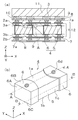
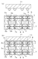
図1は、本発明の実施の形態に係る電子部品内蔵型配線基板12を示す概略の断面図であり、電子部品内蔵型配線基板12の一方の主面(上面)側に電子素子11を搭載した状態の断面図を示している。電子部品内蔵型配線基板12は、絶縁基材1と絶縁基材1の内部に埋設された電子部品4とを備えている。電子部品4は、絶縁基材1内に空隙を形成して、空隙の内部に収容され埋設されている。このように、電子部品内蔵型配線基板12は、絶縁基材1内に電子部品4が内蔵されたものである。
FIG. 1 is a schematic cross-sectional view showing an electronic component built-in
絶縁基材1は、図1に示すように、一方の主面(上面1a)に複数の第1の電極パッド2aが設けられ、第1の電極パッド2aの下方の他方の主面(下面1b)に複数の第2の電極パッド2bが設けられている。第1の電極パッド2aは、電子部品内蔵型配線基板1
2に搭載される電子素子11と電気的に接続され、第1の電極パッドと第2の電極パッド2bとは対向するように配置され、電気的に接続される。電子部品4は、第1の電極パッド2aと第2の電極パッド2bとの間の絶縁基材1内に埋設されている。
As shown in FIG. 1, the
The first electrode pad and the
また、電子部品内蔵型配線基板12は、内部に第1のビアホール導体3aと第2のビアホール導体3bとを有しており、第1のビアホール導体3aが第1の電極パッド2aと電子部品4の外部電極6とを電気的に接続しており、第2のビアホール導体3bが第2の電極パッド2bと電子部品4の外部電極6とを電気的に接続している。
The electronic component built-in
絶縁基材1は、熱硬化性樹脂を含んでおり、熱膨張係数または弾性率を容易に調整する上で、例えば、無機質の粒状フィラーと有機樹脂とからなる絶縁材料を用いることができる。また、絶縁基材1は、機械的強度を高める上で、例えば、ガラス繊維またはアラミド繊維等の繊維状フィラーと有機樹脂とからなる絶縁材料を用いることができる。
The
また、無機質の粒状フィラーは、例えば、SiO2、Al2O3およびBaTiO3の群から選ばれる少なくとも1種を好適に用いることができる。無機質の粒状フィラーとして、SiO2を用いた場合には絶縁層の比誘電率を小さくすることができる。また、無機質の
粒状フィラーとして、Al2O3を用いた場合には配線基板の熱伝導率を高めることができる。無機質の粒状フィラーとして、BaTiO3を用いた場合には絶縁層の比誘電率を高
めることができる。特に、電子機器の小型化または高性能化を目的として、高速伝送を行うためには、無機質の粒状フィラーとして低誘電率のSiO2を用いることが望ましい。
As the inorganic particulate filler, for example, at least one selected from the group of SiO 2 , Al 2 O 3 and BaTiO 3 can be suitably used. When SiO 2 is used as the inorganic particulate filler, the dielectric constant of the insulating layer can be reduced. Further, when Al 2 O 3 is used as the inorganic particulate filler, the thermal conductivity of the wiring board can be increased. When BaTiO 3 is used as the inorganic particulate filler, the dielectric constant of the insulating layer can be increased. In particular, in order to perform high-speed transmission for the purpose of miniaturization or high performance of electronic equipment, it is desirable to use SiO 2 having a low dielectric constant as an inorganic particulate filler.
また、絶縁基材1は、熱硬化性樹脂を含んでおり、熱硬化性樹脂としては、ポリフェニレンエーテル(APPE)系樹脂、エポキシ系樹脂およびシアネート系樹脂の群から選ばれる少なくとも1種が好ましい。APPE系樹脂は、比誘電率、誘電損失および吸水率が低く、さらに、ガラス転移点が高いため、高耐熱性であることから、特に好ましい。さらに、絶縁基材1の混合物は、無機質の粒状フィラーとのぬれ性を改善するために、分散剤またはカップリング剤等を含んでもよい。
The
第1のビアホール導体3aおよび第2のビアホール導体3bは、めっき層からなり、図1に示すように、第1のビアホール導体3aが絶縁基材1の一方の主面(上面1a)の第1電極極パッド2aと電子部品4の外部電極6とを電気的に接続しており、第2のビアホール導体3bが他方の主面(下面1b)の第2の電極パッド2bと絶縁基材1内の電子部品4の外部電極6とを電気的に接続している。また、第1のビアホール導体3a(第2のビアホール導体3b)は、図4(a)に示すように、絶縁基材1の厚み方向に直交する方向の断面形状が略円形状となるように設けられており、絶縁基材1の表面(上面1aまたは下面1b)方向に向かって漸次拡径する略逆円錐台形状で形成されている。また、第1のビアホール導体3a(第2のビアホール導体3b)は、例えば、銅(Cu)めっき層からなる。
The first via-
また、第1のビアホール導体3(第2のビアホール導体3b)は、絶縁基材1にビアホールを形成してビアホール内の外部電極6の上面側延在部6A(下面側延在部6C)を覆うようにめっき処理を行なうことによって形成することができる。具体的には、第1のビアホール導体3a(第2のビアホール導体3b)は、外部電極6の上面側延在部6B(下面側延在部6C)が露出するように絶縁基材1内にビアホールを形成して、上面側延在部6B(下面側延在部6C)を覆うとともに、外部電極6と第1の電極パッド2a(第2の電極パッド2b)とが電気的に接続するようにビアホール内に形成される。
The first via-hole conductor 3 (second via-
電子部品内蔵型配線基板12は、図1(a)に示すように、電子部品4が絶縁基材1の熱硬化性樹脂内に内蔵されている。図1(b)および図2は、電子部品内蔵型配線基板1
2に内蔵されている電子部品4を取り出して電子部品4の単体を示したものである。電子部品4は、例えば、積層型コンデンサであり、絶縁基材1内に埋設されて、外部電極6が第1のビアホール導体3aおよび第2のビアホール導体3bと電気的に接続されている。
As shown in FIG. 1A, the electronic component built-in
The
電子部品4は、第1の電極パッド2aと第2の電極パッド2bとの間の絶縁基材1内に埋設されており、積層体5と一対の外部電極6とを有している。積層体5は、直方体状であり、上面、下面、一対の側面および一対の端面を有している。図2に示すように、一対の外部電極6は、電極側面部6Aと上面側延在部6Bと下面側延在部6Cとを含んでいる。電極側面部6Aは、積層体5の端面1e(端面1f)に設けられ、上面側延在部6Bは、電極側面部6Aから上面1aに延在しており、下面側延在部6Cは、電極側面部6Aから下面1bに延在している。
The
電子部品内蔵型配線基板12は、電子部品4として積層型コンデンサが内蔵されているが、内蔵する電子部品4は、積層型コンデンサに限らない。電子部品4は、例えば、低抗部品またはインダクタ部品等の外部電極を有するものであってもよい。以下では、電子部品4として積層型コンデンサが電子部品内蔵型配線基板12に用いられる場合について説明する。
The electronic component built-in
積層型コンデンサは、図1および図2に示すように、積層体5と積層体5のそれぞれの端面1e、1fに設けられた一対の外部電極6とを有しており、セラミック材料の誘電体層と内部電極(第1の内部電極5aおよび第2の内部電極5b)とが交互に積層されている。一対の外部電極6は、積層体5の端面1e、1fに引き出された内部電極(第1の内部電極5aおよび第2の内部電極5b)に電気的に接続されている。
As shown in FIGS. 1 and 2, the multilayer capacitor includes a
積層型コンデンサは、積層体5が複数の誘電体層が積層されて略直方体状に形成されており、互いに対向する一対の主面(上面1aおよび下面1b)と互いに対向する一対の側面1c、1dと互いに対向する一対の端面1e、1fとを有し、互いに対向する一対の端面1e、1fに外部電極6が形成されている。このように、一対の端面1e、1fが一対の主面(上面1aおよび下面1b)間に位置するとともに一対の主面(上面1aおよび下面1b)に直交しており、一対の側面1c、1dが、一対の主面(上面1aおよび下面1b)間に位置するとともに一対の主面(上面1aおよび下面1b)1a、1bに直交しており、一対の端面1e、1fと一対の側面1c、1dとが直交している。なお、略直方体状とは、立方体形状または直方体形状のみならず、例えば、直方体の稜線部分に面取りが施され、稜線部分がR形状となっているものを含んでいる。誘電体層となるセラミックグリーンシートを複数枚積層して焼成することで得られる焼結体である。
In the multilayer capacitor, the
積層体4は、誘電体層の表面に内部電極5a、5bが形成されたセラミックグリーンシートを複数枚積層して焼成することで得られる焼結体である。このように、積層体5は、略直方体状に形成されており、誘電体層および内部電極(第1の内部電極5aおよび第2の内部電極5b)の積層方向(Z方向)に直交する方向の断面(XY面)となる平面が長方形状となっている。
The
積層型コンデンサは、長手方向(X方向)の長さが、例えば、0.6(mm)〜2.2(mm)、短手方向(Y方向)の長さが、例えば、0.3(mm)〜1.5(mm)、高さ方向(Z方向)の長さが、例えば、0.3(mm)〜1.2(mm)である。 The multilayer capacitor has a length in the longitudinal direction (X direction) of, for example, 0.6 (mm) to 2.2 (mm), and a length in the short side direction (Y direction) of, for example, 0.3 ( mm) to 1.5 (mm) and the length in the height direction (Z direction) is, for example, 0.3 (mm) to 1.2 (mm).
誘電体層は、積層方向(Z方向)からの平面視において長方形状である。図2に示した誘電体層および内部電極(第1の内部電極5aおよび第2の内部電極5b)の構造は模式的なものであり、実際には数層〜数百層の誘電体層と内部電極(第1の内部電極5aおよび第2の内部電極5b)とが積層されたものが多く用いられており、1層当たりの厚みが
、例えば、0.2(μm)〜3(μm)である。積層体4は、例えば、10(層)〜1000(層)からなる複数の誘電体層と内部電極(第1の内部電極5aおよび第2の内部電極5b)とがZ方向に積層されている。また、積層体5内の内部電極(第1の内部電極5aおよび第2の内部電極5b)の積層数は、積層型コンデンサの特性等に応じて適宜に設定される。
The dielectric layer has a rectangular shape in plan view from the stacking direction (Z direction). The structure of the dielectric layers and internal electrodes (first
誘電体層は、例えば、チタン酸バリウム(BaTiO3)、チタン酸カルシウム(CaTiO3)、チタン酸ストロンチウム(SrTiO3)またはジルコン酸カルシウム(CaZrO3)等が用いられる。また、誘電体層は、高い誘電率の点から、特に、誘電率の高い強誘電体材料としてチタン酸バリウムを用いることが好ましい。 For example, barium titanate (BaTiO 3 ), calcium titanate (CaTiO 3 ), strontium titanate (SrTiO 3 ), or calcium zirconate (CaZrO 3 ) is used for the dielectric layer. The dielectric layer preferably uses barium titanate as a ferroelectric material having a high dielectric constant from the viewpoint of a high dielectric constant.
内部電極は、図2に示すように、積層体5の積層方向において第1の内部電極5aと第2の内部電極5bとが対向しており、第1の内部電極5aが誘電体層間に配置されて、一方の端部が一方の端面1eに引き出されており、また、第2の内部電極5bが誘電体層間に配置されて、一方の端部が一方の端面1eに対向する他方の端面1fに引き出されている。
As shown in FIG. 2, in the internal electrode, the first
第1の内部電極5aおよび第2の内部電極5bの導電材料は、例えば、ニッケル(Ni)、銅(Cu)、銀(Ag)、パラジウム(Pd)または金(Au)等の金属材料、あるいは、これらの金属材料の一種以上を含む、例えば、Ag−Pd合金等の合金材料である。また、第1の内部電極5aおよび第2の内部電極5bは、電極の厚みが、例えば、0.2(μm)〜2(μm)であり、用途に応じて厚みを適宜に設定すればよい。また、第1の内部電極5aおよび第2の内部電極5bは、同一の金属材料または合金材料によって形成することが好ましい。
The conductive material of the first
一対の外部電極6は、積層体5の長手方向に位置する端面1e、1fにそれぞれ設けられており、図2(b)に示すように、一方が端面1eに引き出された第1の内部電極5aを覆うように形成され、第1の内部電極5aに電気的に接続されており、また、他方が端面1fに引き出された第2の内部電極5bを覆うように形成され、第2の内部電極5bに電気的に接続されている。
The pair of
図2に示すように、一対の外部電極6は、一方の外部電極6が端面1eに設けられるとともに、端面1eの電極側面部6Aから上面1aおよび下面1bの表面にそれぞれ延在して設けられており、上面1aに上面側延在部6Bおよび下面1bに下面側延在部6Cを有しており、また、一方の外部電極6と同じように、他方の外部電極6が端面1fに設けられるとともに、端面1fの電極側面部6Aから上面1aおよび下面1bの表面にそれぞれ延在して設けられており、上面1aに上面側延在部6Bおよび下面1bに下面側延在部6Cを有している。
As shown in FIG. 2, the pair of
一対の外部電極6は、図1および図2に示すように、上面側延在部6Bが第1のビアホール導体3aを介して第1の電極パッド2aと接続され、下面側延在部6Cが第2のビアホール導体3bを介して第2の電極パッド2bと接続されている。また、図2に示すように、上面側延在部6Bおよび下面側延在部6Cは、延在方向において積層方向から平面視して中央部が端部よりも突出している。
As shown in FIGS. 1 and 2, the pair of
電子部品内蔵型配線基板12は、一方の主面(上面1a)側で外部電極6の上面側延在部6Bが第1のビアホール導体3aを介して第1の電極パッド2aに接続され、他方の主面(下面1b)側で外部電極6の下面側延在部6Cが第2のビアホール導体3bを介して第2の電極パッド2bで接続されており、第1の電極パッド2aと第2の電極パッド2bとは、厚み方向において第1のビアホール導体3aと外部電極6と第2のビアホール導体
3bとを介して繋がっている。このように、電子部品内蔵型配線基板12は、一方の主面(上面1a)の第1の電極パッド2aから他方の主面(下面1b)の第2の電極パッド2bに向かって、厚み方向において第1のビアホール導体3aと外部電極6と第2のビアホール導体3bとによって内部に熱を放熱するための放熱経路が形成されることになる。
The electronic component built-in
したがって、電子部品内蔵型配線基板12は、一方の主面(上面1a)側の第1の電極パッド2aに電子素子が電気的に接続されるので、一方の主面(上面1a)側の第1の電極パッド2aから他方の主面(下面1b)側の第2の電極パッド2bに向かって電子素子11から生じた熱を効果的に伝えて放熱することができる。
Accordingly, the electronic component built-in
また、図2(a)に示すように、上面側延在部6Bおよび下面側延在部6Cは、上面1aおよび下面1bの中央部に向かって円弧状に湾曲して延在している。すなわち、図2(a)に示すように、上面側延在部6B(下面側延在部6C)は、積層体4の短手方向(Y方向)の長さが端面1e(端面1f)側から上面1a(下面1b)の中央部側に向かって漸次小さくなるように上面1aおよび下面1bの中央部側に突出するように凸状に湾曲しており、中央部側に向かって湾曲して延在する湾曲部を有している。このように、上面側延在部6B(下面側延在部6C)は、中央部側に向かって凸状に湾曲する湾曲部を有しており、湾曲部は、例えば、凸状に湾曲する円弧状である。
Further, as shown in FIG. 2A, the upper surface
例えば、電子部品内蔵型配線基板は、一方の主面(上面)の第1の電極パッドから他方の主面(下面)の第2の電極パッドに向かって、厚み方向において第1のビアホール導体と外部電極と第2のビアホール導体とによって内部に放熱経路が形成されると、構成部材、例えば、絶縁基材、絶縁基材内部の配線パターン、第1のビアホール導体および第2のビアホール導体等の線膨張係数の違いによって、上面側延在部および下面側延在部に応力が集中しやくなり、剥がれまたはクラック等が生じやすくなる。 For example, the electronic component built-in wiring board includes a first via-hole conductor in the thickness direction from the first electrode pad on one main surface (upper surface) to the second electrode pad on the other main surface (lower surface). When a heat dissipation path is formed inside the external electrode and the second via-hole conductor, components such as an insulating base, a wiring pattern inside the insulating base, the first via-hole conductor, the second via-hole conductor, etc. Due to the difference in the coefficient of linear expansion, stress tends to concentrate on the upper surface side extending portion and the lower surface side extending portion, and peeling or cracking is likely to occur.
しかしながら、電子部品内蔵型配線基板12は、上面側延在部6B(下面側延在部6C)が上面1aおよび下面1bの中央部に向かって凸状に湾曲して延在しているので、構成部材の線膨張係数の違いによって発生する応力が凸状の湾曲部で効果的に分散される。したがって、電子部品内蔵型配線基板12は、応力の集中が抑制されるので、剥がれまたはクラック等の発生が抑制される。このように、電子部品内蔵型配線基板12は、上面側延在部6B(下面側延在部6C)を凸状に湾曲して延在することによって、電子部品4の信頼性の低下を抑制することができる。
However, in the electronic component built-in
電子部品内蔵配線基板12は、内蔵される電子部品4の外部電極6と第1のビアホール導体3aおよび第2のビアホール導体3bとからなる放熱経路を絶縁基材1の内部に設けることによって、一方の主面(上面1a)側に搭載される電子素子11に対する放熱性を向上させるとともに、上面側延在部6B(下面側延在部6C)が延在方向において上面1aおよび下面1bの中央部に向かって凸状に湾曲して延在しているので、応力の集中を抑制することができる。
The electronic component built-in
また、一対の外部電極6は、上面側延在部6B(下面側延在部6C)が湾曲した凸状となるように中央部を突出させており、上面側延在部6B(下面側延在部6C)の面積が大きくなり、熱容量が大きくなるので、放熱性を向上させることができる。
The pair of
また、上面側延在部6B(下面側延在部6C)は、形状をR(曲率半径)を有する湾曲状の角のない形状とすることにより、上面側延在部6B(下面側延在部6C)が積層体5から剥離しにくくなる。
Further, the upper surface
積層型コンデンサは、図1に示すように、積層体5の表面の外部電極6の一部が第1の
ビアホール導体3aおよび第2のビアホール導体3bと接続されている。具体的には、電子部品内蔵型配線基板12は、第1のビアホール導体3aおよび第2のビアホール導体3bが、図1乃至図3に示すように、積層体5の表面の外部電極6の上面側延在部6Bおよび下面側延在部6Cのエッチング処理領域6dで外部電極6と直接的に接続されている。
In the multilayer capacitor, as shown in FIG. 1, a part of the
このように、積層型コンデンサは、絶縁基材1内で外部電極6と第1のビアホール導体3aおよび第2のビアホール導体3bとが直接的に接続されており、図1に示すように、一対の外部電極6は、絶縁基材1内で第1のビアホール導体3aおよび第2のビアホール導体3bに接する領域と熱硬化性樹脂に接する領域とを有することになる。積層型コンデンサは、エッチング処理領域6dが第1のビアホール導体3aおよび第2のビアホール導体3bに接する領域であり、外部電極6は、第1のビアホール導体3aおよび第2のビアホール導体3bに接する領域(エッチング処理領域6d)の表面粗さ(Ra)が熱硬化性樹脂に接する領域の表面粗さ(Ra)よりも小さい。なお、絶縁基材1内での第1のビアホール導体3aおよび第2のビアホール導体3bと外部電極6との接続については後述する。
Thus, in the multilayer capacitor, the
一対の外部電極6は、下地電極6aと下地電極を覆う金属層6bとを含んでおり、一対の下地電極6aは、一方が端面1eから上面1aおよび下面1bに延在するように形成され、また、他方が端面1fから上面1aおよび下面1bに延在するように形成されている。金属層6bは、下地電極6aを覆うように下地電極5の表面上に形成されている。このように、一対の外部電極6は、下地電極6aと金属層6bとから構成されており、端面1eにおいて、上面1aから下面1bにわたって設けられており、端面1fにおいて、上面1aから下面1bにわたって設けられている。
The pair of
下地電極6aの導電材料は、例えば、Cu(銅)、ニッケル(Ni)、銀(Ag)、パラジウム(Pd)または金(Au)等の金属材料、あるいは、これらの金属材料の一種以上を含む、例えば、Cu−Ni合金等の合金材料である。また、一対の下地電極4は、積層体1の表面に同一の金属材料または同一の合金材料によって形成することが好ましい。
The conductive material of the
外部電極6の下地電極6aは、端面1e、1fに引き出された第1の内部電極5aまたは第2の内部電極5bに電気的に接続されている。また、下地電極6aの導電材料は、例えば、銅(Cu)、ニッケル(Ni)、銀(Ag)、パラジウム(Pd)または金(Au)等の金属材料、あるいは、これらの金属材料の一種以上を含む、例えば、Cu−Ni合金等の合金材料である。また、下地電極6aは、例えば、上述の金属材料または合金材料にガラス成分を混合して調製した導電性ペーストが用いられる。一対の下地電極6aは、セラミック本体5の表面に同一の金属材料または同一の合金材料によって形成することが好ましい。
The
下地電極6aは、主面(上面1aおよび下面1b)における厚みが、例えば、4(μm)〜10(μm)であり、端面1e、1fにおける厚みが、例えば、10(μm)〜25(μm)であり、側面1c、1dにおける厚みが、例えば、4(μm)〜10(μm)である。
The
下地電極6aは、積層体5の表面に形成されており、めっき層6bは、下地電極6aの全体を覆うように下地電極6aに形成されている。また、めっき層6bは、図2に示すように、ニッケル(Ni)めっき層6b1と銅(Cu)めっき層6b2とを含んでおり、ニッケル(Ni)めっき層6b1は下地電極6aを覆うように形成されており、また、銅(Cu)めっき層6b2はニッケル(Ni)めっき層6b1を覆うように形成されている。銅(Cu)めっき層6b2は、表面に凹凸部6cを有しており、凹凸部6cは絶縁基材1の熱硬化性樹脂との密着性を向上させる。
The
このように、ニッケル(Ni)めっき層6b1は、下地電極6aと銅(Cu)めっき層6b2との間に形成されており、内側の下地電極6aを保護することができる。具体的には、第1のビアホール導体3(第2のビアホール導体3b)はめっき層で形成されており、絶縁基材1内にめっき処理を行なって第1のビアホール導体3a(第2のビアホール導体3b)を形成する場合には、このめっき処理の前にビアホールの内部に対してエッチング処理が行なわれる。このエッチング処理は、ビアホール内の銅(Cu)めっき層6b2の酸化膜を除去するとともに銅(Cu)めっき層6b2の表面を平坦にするために行なうものである。また、このエッチング処理は、ビアホール形成時のレーザ加工でビアホールの側面が凹凸となっており、この凹凸を平坦にするために行なうものである。
Thus, the nickel (Ni) plating layer 6b1 is formed between the
このエッチング処理では、特に、めっき層6bの表面の銅(Cu)めっき層6b2がエッチング処理される。かりに、エッチング液が銅(Cu)めっき層6b2から下地電極6aに侵入しようとしても、ニッケル(Ni)めっき層6b1は、下地電極6aと銅(Cu)めっき層6b2との間に形成されており、緻密なめっき層であり、また、酸化しやすく、酸化被膜を有しているので、エッチングされにくく、エッチング処理の際にエッチング液の下地電極6aへの侵入を抑制するので、下地電極6aを保護することができる。
In this etching process, in particular, the copper (Cu) plating layer 6b2 on the surface of the
具体的には、例えば、銅(Cu)めっき層6b2をエッチング処理する場合には、一般的に酸系のエッチング液が用いられており、一方、ガラス成分を含有する下地電極6aは内部に間隙を有しているので、下地電極6aの内部の間隙をエッチング液が通過して積層体5に到達すると、酸系のエッチング液で誘電体層または内部電極(第1の内部電極5aおよび第2の内部電極5b)が腐食して絶縁性の低下が生じやすくなる。しかしながら、電子部品内蔵型配線基板12は、ニッケル(Ni)めっき層6b1が形成されているので、エッチング液が下地電極6aに侵入するのを抑制することができる。
Specifically, for example, when the copper (Cu) plating layer 6b2 is etched, an acid-based etching solution is generally used, while the
また、かりに、銅(Cu)めっき層6b2がオーバーエッチングされたとしても、ニッケル(Ni)めっき層6b1が下地電極6aと銅(Cu)めっき層6b2との間に形成されているので、下地電極6aを保護することができる。すなわち、エッチング処理において、かりに、エッチング量が大きくなったとしても、下地電極6aへのエッチング液の侵入が銅(Cu)めっき層6b2によって抑制されるので、積層型コンデンサは、外部電極6に対するエッチング処理の自由度を高めることができる。
Even if the copper (Cu) plating layer 6b2 is over-etched, the nickel (Ni) plating layer 6b1 is formed between the
ニッケル(Ni)めっき層6b1は、図2に示すように、下地電極6aを覆うように下地電極6aの表面上に形成されている。ニッケル(Ni)めっき層6b1は、ニッケル(Ni)を含むものであり、厚みが、例えば、2(μm)〜10(μm)である。
As shown in FIG. 2, the nickel (Ni) plating layer 6b1 is formed on the surface of the
銅(cu)めっき層6b2は、図2に示すように、ニッケル(Ni)めっき層6b1の外側に形成されている。銅(cu)めっき層6b2は、銅(Cu)を含むものであり、厚みが、例えば、5(μm)〜12(μm)である。めっき層6bは、例えば、電解めっき法等を用いてニッケル(Ni)めっき層6b1と銅(Cu)めっき層6b2とを連続して形成することができる。
As shown in FIG. 2, the copper (cu) plating layer 6b2 is formed outside the nickel (Ni) plating layer 6b1. The copper (cu) plating layer 6b2 contains copper (Cu) and has a thickness of, for example, 5 (μm) to 12 (μm). For example, the
また、銅(Cu)めっき層6b2は、第1のビアホール導体3a(第2のビアホール導体3b)が銅(Cu)めっき層を含んで形成されており、第1のビアホール導体3a(第2のビアホール導体3b)と外部電極6との接続信頼性を向上させることができる。このように、銅(Cu)めっき層6b2は、第1のビアホール導体3a(第2のビアホール導体3b)との電気的な接続を良好にするために、第1のビアホール導体3a(第2のビアホール導体3b)の材質である銅(Cu)を含むことが好ましい。
The copper (Cu) plating layer 6b2 includes the first via-
積層型コンデンサは、図2に示すように、外部電極6の表面に凹凸部6cが形成されており、表面の凹凸部6cは表面粗さ(Ra)が2(μm)以下となるように設けられている。また、エッチング処理領域6dは、銅(Cu)めっき層6b2の凹凸部6cをエッチング処理することによって形成されており、他の領域(領域6d以外の領域)と比べて表面がより平坦となっている。
As shown in FIG. 2, the multilayer capacitor has an
外部電極6の表面の凹凸部6cに対してエッチング処理を行なう場合には、エッチング処理領域6dが平坦になるように、表面の凹凸部6cは、表面粗さ(Ra)が2(μm)以下となるように設けられている。一方、表面粗さ(Ra)が2(μm)より大きくなると、均一なエッチング処理が行われにくくなり、エッチング処理領域6dが平坦になりにくく、後述するように、第1のビアホール導体3a(第2のビアホール導体3b)が均一なめっき層として形成されにくくなる。
When the etching process is performed on the
また、凹凸部6cは、銅(Cu)めっき層6b2の形成において添加剤として金属光沢剤を添加しためっき液を用いることによって、表面粗さ(Ra)が2(μm)以下となるように表面形状が調整される。なお、表面粗さ(Ra)は、中心線平均粗さ(Ra)であり、例えば、表面粗さ測定器を用いて測定することができる。
The
また、銅(Cu)めっき層6b2は、凹凸部6cの表面粗さ(Ra)を小さくすると、少ないエッチング量で表面が平坦になりやすく、表面を平坦にするためにオーバーエッチングしなくてもよいので、めっき層の厚みを薄くすることができる。このように、積層型コンデンサは、凹凸部6cの表面粗さ(Ra)を小さくして、好ましくは、外部電極6の表面粗さ(Ra)を1(μm)以下にして、銅(Cu)めっき層6b2の全体の厚みを薄くすることによって、厚み方向(Z方向)の寸法を小さくすることができる。
Further, when the surface roughness (Ra) of the
ここで、絶縁基材1内での第1のビアホール導体3a(第2のビアホール導体3b)と外部電極6との接続について以下に説明する。
Here, the connection between the first via-
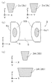
図3(a)は、図1に示す電子部品内蔵型配線基板12において第1のビアホール導体3aと外部電極6との接続部を示すA領域の拡大図である。また、図3(b)は、図3(a)の拡大図から第1のビアホール導体3aを除いた外部電極6の表面のエッチング処理領域6dの状態を示す拡大図である。また、図3(c)は、外部電極6の表面にエッチング処理領域6dが形成される前の外部電極6の状態を示す拡大図であり、破線で示すようにエッチング処理領域6dに対応する領域には凹凸部6cが形成されている。なお、第2のビアホール導体3bと外部電極6との接続部についても同様であり、以下では、第1のビアホール導体3aと外部電極6との接続部について説明する。
FIG. 3A is an enlarged view of a region A showing a connection portion between the first via-
電子部品内蔵型配線基板12は、図1および図3に示すように、第1のビアホール導体3aが外部電極6の上面側延在部6Bの表面のエッチング処理領域6dで外部電極6と直接的に接続されており、外部電極6の上面側延在部6Bのエッチング処理領域6dが第1のビアホール導体3aとの接続部となっている。
As shown in FIGS. 1 and 3, the electronic component built-in
外部電極6は、図3(b)に示すように、エッチング処理領域6dが他の領域(エッチング処理領域6d以外の領域)と比べて表面粗さ(Ra)が小さく、表面がより平坦となっており、表面粗さ(Ra)がエッチング処理領域6dと他の領域(エッチング領域6d以外の領域)とでは異なっている。外部電極6は、図3(c)に示すように、エッチング処理領域6dとなる領域においてエッチング処理前には凹凸部6cを有しており、この凹凸部6cに対してエッチング処理を行なってエッチング処理領域6dを平坦にしている。
As shown in FIG. 3B, the
したがって、外部電極6は、エッチング処理を行なうことによってエッチング処理領域
6dと他の領域(エッチング領域6d以外の領域)とで表面粗さ(Ra)が異なっており、エッチング処理領域6dの表面粗さ(Ra)が熱硬化性樹脂と接する領域の表面粗さ(Ra)よりも小さくなっている。このように、電子部品内蔵型配線基板12は、積層型コンデンサが絶縁基材1内に埋設されており、積層型コンデンサは、エッチング処理領域6dと絶縁基材1内で熱硬化性樹脂に接する領域とにおいて外部電極6の上面側延在部6Bの表面粗さ(Ra)が異なっている。
Therefore, the
具体的には、ビアホールは絶縁基材1内に外部電極6の上面側延在部6Bの表面が露出するように形成される。そして、エッチング処理領域6dは、ビアホール内に露出する外部電極6の凹凸部6cに対して凹凸部6cの高低差が小さくなるようにエッチング処理を行なうことによって形成される。ビアホール内をめっき処理することによって、第1のビアホール導体3aは、エッチング処理された外部電極6の表面を覆うとともに、外部電極6と電極パッド2aとを電気的に接続するように絶縁基材1内のビアホール内にめっき層として形成される。
Specifically, the via hole is formed in the insulating
エッチング処理領域6dは、図2(b)および図3(b)では、平坦な状態として示しているが、表面粗さ(Ra)が1(μm)以下となるような凹凸部を有していてもよい。すなわち、エッチング処理領域6dは、他の領域よりも凹凸部の高低差が小さくなるように形成されており、平坦とは、エッチング処理領域6dが平坦な場合だけを含むものでなく、表面粗さ(Ra)が1(μm)以下となるような凹凸部を有している場合も含んでいる。
The etched
このように、外部電極6は、図2および図3に示すように、上面側延在部6Bおよび下面側延在部6Cの表面に凹凸部6cを有しており、外部電極6の上面側延在部6Bおよび下面側延在部6Cのうち第1のビアホール導体3aおよび第2のビアホール導体3bとの接続部のエッチング処理領域6dの表面のみが平坦となっている。したがって、積層型コンデンサは、外部電極6のエッチング処理領域6dの表面が平坦となり、外部電極6のエッチング処理領域6d以外の領域の表面に凹凸部6cを有することになり、エッチング処理領域6dで外部電極6と第1のビアホール導体3aおよび第2のビアホール導体3bとが直接的に接続される。すなわち、外部電極6は、エッチング処理領域6dの表面が平坦な領域となり、めっき層からなる第1のビアホール導体3aおよび第2のビアホール導体3bは、エッチング処理領域6dで外部電極6と直接的に接続されることになる。
Thus, as shown in FIGS. 2 and 3, the
第1のビアホール導体3aおよび第2のビアホール導体3bは、めっき層で形成されており、銅(Cu)めっき層6b2の表面のエッチング処理領域6dにめっき処理を行なうことによって、外部電極6の上面側延在部6Bおよび下面側延在部6Cの銅(Cu)めっき層6b2上に形成される。したがって、エッチング処理領域6dにおいて銅(Cu)めっき層6b2上にめっき処理を行なうことによって、第1のビアホール導体3aおよび第2のビアホール導体3bは、銅(Cu)めっき層6b2上に均一なめっき層として形成されるので、外部電極6との接続信頼性を向上させることができる。
The first via-
また、第1のビアホール導体3aおよび第2のビアホール導体3bは、ビアホール内の平坦な銅(Cu)めっき層6b2上およびビアホール内の側面において均一なめっき層として成長するので、絶縁基材1の表面の第1の電極パッド2aおよび第2の電極パッド2bとの電気的な接続信頼性も良好なものとなる。したがって、第1のビアホール導体3aおよび第2のビアホール導体3bは、外部電極6との接続信頼性を向上させるとともに第1の電極パッド2aおよび第2の電極パッド2bとの接続信頼性も良好なものとすることができる。
Further, the first via
また、積層型コンデンサは、絶縁基材1の熱硬化性樹脂に接する領域においては外部電
極6が凹凸部6cを有しており、熱硬化性樹脂が凹凸部6cに侵入することによってアンカー効果が高まるので、外部電極6と絶縁基材1との密着性を向上させることができる。
In the multilayer capacitor, the
ここで、図1に示す電子部品内蔵型配線基板12に用いられる第1のビアホール導体3a(第2のビアホール導体3b)の他の例の第1のビアホール導体3A(第2のビアホール導体3B)について以下に説明する。図4(b)は、エッチング処理領域6d1を示しており、ビアホール導体3A(第2のビアホール導体3B)に対してエッチング処理領域6d1が用いられる。
Here, the first via-
また、図4(c)は、第1のビアホール導体3A(第2のビアホール導体3B)をX方向およびY方向から視た模式的な断面図であり、ビアホール導体3Aの形状を説明するためのものである。ビアホール導体3A(第2のビアホール導体3B)は、図4(b)および図4(c)に示すように、絶縁基材1の厚み方向に直交する方向の断面形状が略楕円形状となるように設けられており、絶縁基材1の表面方向に向かって漸次拡径する略逆楕円錐台形状で形成されている。すなわち、ビアホール導体3A(第2のビアホール導体3B)は、絶縁基材1の厚み方向に直交する方向の断面形状が楕円形状であり、楕円形状の長径が積層体5の端面1e、1fに略平行となるような略逆楕円錐台形状で形成されている。
FIG. 4C is a schematic cross-sectional view of the first via-
このように、ビアホール導体3A(第2のビアホール導体3B)は、略逆楕円錐台形状で形成することによって、略逆円錐台形状と比べて外部電極6との接続面積が大きくなり、外部電極6との接続を確実に確保することができるので、外部電極6との接続信頼性をさらに向上させることができる。
Thus, by forming the via-
また、ビアホール導体3A(第2のビアホール導体3B)は、かりに、ビアホール導体3A(第2のビアホール導体3B)の形成位置がX方向(外部電極6の長手方向)にずれたとしても、略逆楕円錐台形状で形成されているので、外部電極6との接続信頼性を確保することができる。
Further, the via
ここで、電子部品内蔵型配線基板12の製造方法についての一例を以下に説明する。
Here, an example of a method for manufacturing the electronic component built-in
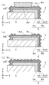
まず、図5(a)に示すように、未硬化の熱硬化性樹脂を含む第1乃至第3の絶縁シート1Aa、1Ab、1Acをそれぞれ準備する。第1乃至第3の絶縁シートは、ポリフェニレンエーテル系樹脂またはエポキシ系樹脂等の熱硬化性樹脂と、SiO2またはAl2O3等の不定形の無機室フィラーとの混合材料からなる。未硬化状態の第1乃至第3の絶縁
シート1Aa、1Ab、1Acは、80(μm)〜150(μm)の厚みでドクターブレードを用いて作製される。
First, as shown to Fig.5 (a), the 1st thru | or 3rd insulation sheets 1Aa, 1Ab, and 1Ac containing uncured thermosetting resin are each prepared. The first to third insulating sheets are made of a mixed material of a thermosetting resin such as polyphenylene ether resin or epoxy resin, and an amorphous inorganic chamber filler such as SiO 2 or Al 2 O 3 . The uncured first to third insulating sheets 1Aa, 1Ab, and 1Ac are produced using a doctor blade with a thickness of 80 (μm) to 150 (μm).
また、図5(a)に示すように、第2の絶縁シート1Abは第1の電極パッド2aを形成するための金属層が、第3の1Acは第2の電極パッド2bを形成するための金属層が表面に設けられており、金属層は、例えば、銅箔またはアルミニウム箔等の金属箔である。
Also, as shown in FIG. 5A, the second insulating sheet 1Ab is a metal layer for forming the
次に、第1の絶縁シート1Aaに電子部品4を収容して埋設するための空隙1aaを形成する。また、電子部品4は、上述したように、例えば、積層型コンデンサであり、積層体5と積層体5の端面に設けられた一対の外部電極6を有しており、外部電極6の上面側延在部6Bおよび下面側延在部6Cが、表面に凹凸部6cを有するとともに、下地電極6aとニッケルめっき層6b1および銅めっき層6b2とを含んでいる。なお、以下では、内蔵する電子部品4として積層型コンデンサを用いる場合について説明する。
Next, a gap 1aa for accommodating and embedding the
図5(b)に示すように、積層型コンデンサを第1の絶縁シート1Aaの空隙1aaに配置し、積層型コンデンサを配置した第1の絶縁シート1Aaの上下に第2および第3の絶縁シート1Abおよび1Acを積層して仮積層体1Aを形成する。 As shown in FIG. 5B, the multilayer capacitor is disposed in the gap 1aa of the first insulating sheet 1Aa, and the second and third insulating sheets are disposed above and below the first insulating sheet 1Aa on which the multilayer capacitor is disposed. 1Ab and 1Ac are laminated to form a temporary laminate 1A.
この仮積層体1Aを絶縁シート中の熱硬化性樹脂が溶融する温度範囲よりも低い、例えば、100(℃)〜120(℃)の温度において、例えば、1(MPa)〜4(MPa)の圧力でもって一旦加熱加圧を行ない、積層型コンデンサの外部電極6の表面に形成された凹凸部6cに熱硬化性樹脂を十分に含浸させる。
The temporary laminate 1A is lower than a temperature range in which the thermosetting resin in the insulating sheet melts, for example, at a temperature of 100 (° C.) to 120 (° C.), for example, 1 (MPa) to 4 (MPa). Heating and pressing are performed once with pressure, and the
その後、熱硬化性樹脂が硬化する温度であり、熱硬化性樹脂の溶融温度よりも高い、例えば、140(℃)〜160(℃)の温度において、例えば、4(MPa)〜8(MPa)の圧力でもって加熱加圧を行ない、熱硬化性樹脂を硬化させて、埋設した積層型コンデンサと第1乃至第3の絶縁シートA1a、1Ab、1Acの界面を強固に接着するとともに、第1乃至第3の絶縁シート1Aa、1Ab、1Ac同士を積層密着して、内部に積層型コンデンサが埋設された絶縁基材1となる積層体1AAを作製する。
Then, it is a temperature at which the thermosetting resin is cured, and is higher than the melting temperature of the thermosetting resin, for example, at a temperature of 140 (° C.) to 160 (° C.), for example, 4 (MPa) to 8 (MPa). The thermosetting resin is cured with the pressure of 1 to harden the thermosetting resin to firmly bond the interface between the embedded multilayer capacitor and the first to third insulating sheets A1a, 1Ab, and 1Ac. The third insulating sheets 1Aa, 1Ab, and 1Ac are laminated and adhered to each other to produce a laminated body 1AA that becomes the
図5(c)に示すように、積層体1AAの上下面の表面に第1の電極パッド2aおよび第2の電極パッド2bを形成する。第1の電極パッド2aおよび第2の電極パッド2bは、例えば、周知のフォトリソグラフィー法を用いて、レジスト塗布、露光、現像、エッチング、レジスト除去等の工程を経ることによって形成される。
As shown in FIG. 5C, the
次に、図6(a)に示すように、積層体1AAの第1の電極パッド2aおよび第2の電極パッド2bが形成されている上面および下面の表面側にレーザ加工法を用いて外部電極6の上面側延在部6Bおよび下面側延在部6Cが露出するようにビアホールを形成する。そして、ビアホール内に露出している外部電極6の上面側延在部6Bおよび下面側延在部6Cの凹凸部6cに対してエッチング処理を行なう。このエッチング処理の際には、ビアホール内の外部電極6の上面側延在部6Bおよび下面側延在部6Cの凹凸部6cがエッチング処理されるとともにビアホール内の側面の凹凸もエッチング処理される。エッチング処理によって、上面側延在部6Bおよび下面側延在部6Cにエッチング処理領域6dが形成される。
Next, as shown in FIG. 6A, external electrodes are formed on the upper and lower surface surfaces of the laminate 1AA where the
図6(b)に示すように、エッチング処理された外部電極6の上面側延在部6Bおよび下面側延在部6Cを覆うように、また、第1の電極パッド2aおよび第2の電極パッド2bと外部電極6とが電気的に接続するようにビアホール内をめっき処理して、積層体1AAにめっき層からなる第1のビアホール導体3aおよび第2のビアホール導体3bを形成して、絶縁基材1を作製する。このようにして、積層型コンデンサが内蔵された電子部品内蔵型配線基板12を製造することができる。
As shown in FIG. 6B, the
電子部品内蔵型配線基板12は、図6(c)に示すように、絶縁基材1の上下面に、少なくとも1層の絶縁シート(例えば、周知のプリプレグシート)を用いてさらに上下面に絶縁層7を設けて、絶縁層7上に電子素子11に電気的に接続される電極パッド9を形成することができる。このように、電子部品内蔵型配線基板12は、多層構造の配線基板とすることができる。また、この場合にも、絶縁層に対して上述の製造方法と同様な製造方法を用いて、ビアホール導体7aおよび電極パッド9等を形成することができる。また、最外層には、絶縁層8が電極パッド9およびビアホール導体7aを露出するように設けられている。
As shown in FIG. 6C, the electronic component built-in
また、図7に示すように、例えば、電子素子11の電極パッドと電子部品内蔵型配線基板12の電極パッド9とにはんだを設けてはんだ接合することにより、電子部品内蔵型配線基板12に電子素子11を搭載することができる。
Further, as shown in FIG. 7, for example, soldering is performed on the electrode pads of the
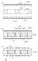
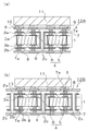
電子部品内蔵型配線基板12は、例えば、図8に示すように構成であってもよい。電子部品内蔵型配線基板12Aは、図8(a)に示すように、一対の外部電極6のうち一方の外部電極6側に配置された第1の電極パッド2aと第2の電極パッド2bとを接続導体2cを介して直接接続している。このような構成により、電子部品内蔵型配線基板12Aはさらに放熱性が向上する。
For example, the electronic component built-in
また、電子部品内蔵型配線基板12Bは、図8(b)に示すように、一対の外部電極6に対応して配置された第1の電極パッド2aと第2の電極パッド2bとを接続導体2cを介して直接接続している。このような構成により、電子部品内蔵型配線基板12Bはさらに放熱性が向上する。
Further, as shown in FIG. 8B, the electronic component built-in wiring board 12B connects the
また、例えば、電子部品内蔵型配線基板12、12A、12Bは、さらに、電子機器に組み込まれるマザーボード等の配線基板上に搭載することができる。放熱性が向上した電子部品内蔵型配線基板12、12A、12Bを電子機器に組み込まれるマザーボード等の配線基板上に搭載することによって、電子機器は、全体として、放熱性が向上するとともに信頼性の低下が抑制されたものとなる。
Further, for example, the electronic component built-in
電子部品内蔵型配線基板12Bは、図5および図6で示すような製造方法を用いて作製することができる。 The electronic component built-in wiring board 12B can be manufactured by using a manufacturing method as shown in FIGS.
上述したような製造方法(図5(a)〜図5(c))を用いて、図9(a)に示すような積層体1AAを作製する。図9(b)に示すように、積層体1AAの第1の電極パッド2aおよび第2の電極パッド2bが形成されている上面および下面の表面側にレーザ加工法を用いて外部電極6の上面側延在部6Bおよび下面側延在部6Cが露出するようにビアホールを形成する。さらに、ドリル加工を用いて接続導体2cを形成する領域に貫通孔を形成する。
Using the manufacturing method as described above (FIGS. 5A to 5C), a laminate 1AA as shown in FIG. 9A is manufactured. As shown in FIG. 9B, the upper surface of the
図9(c)に示すように、ビアホール内に露出している外部電極6の上面側延在部6Bおよび下面側延在部6Cの凹凸部6cに対してエッチング処理を行なう。このエッチング処理の際には、ビアホール内の外部電極6の上面側延在部6Bおよび下面側延在部6Cの凹凸部6cがエッチング処理されるとともにビアホール内の側面の凹凸部もエッチング処理される。また、貫通孔内の内周面の凹凸部もエッチング処理される。
As shown in FIG. 9C, an etching process is performed on the concavo-
そして、図9(c)に示すように、エッチング処理された外部電極6の上面側延在部6Bおよび下面側延在部6Cを覆うように、また、第1の電極パッド2aおよび第2の電極パッド2bと外部電極6とが電気的に接続するようにビアホール内をめっき処理して、積層体1AAにめっき層からなる第1のビアホール導体3aおよび第2のビアホール導体3bを形成とともに、第1の電極パッド2aと第2の電極パッド2bとが電気的に接続するように貫通孔内をめっき処理して、積層体1AAにめっき層からなる接続導体2cを形成して、絶縁基材1を作製する。このようにして、積層型コンデンサが内蔵された電子部品内蔵型配線基板12Bを製造することができる。
Then, as shown in FIG. 9C, the
本発明は、上述した実施の形態に特に限定されるものではなく、本発明の範囲内で種々の変更および改良が可能である。 The present invention is not particularly limited to the above-described embodiments, and various changes and improvements can be made within the scope of the present invention.
1 絶縁基材
1a 第1の絶縁シート
1b 第2の絶縁シート
1c 第3の絶縁シート
2a 第1の電極パッド
2b 第2の電極パッド
2c 接続導体
3a 第1のビアホール導体
3b 第2のビアホール導体
4 電子部品
5 積層体
5a 第1の内部電極
5b 第2の内部電極
6 外部電極
6A 電極側面部
6B 上面側延在部
6C 下面側延在部
6a 下地電極
6b めっき層
6b1 ニッケル(Ni)めっき層
6b2 銅(Cu)めっき層
6c 凹凸部
6d、6d1 エッチング処理領域
12、12A、12B 電子部品内蔵型配線基板
DESCRIPTION OF
Claims (4)
前記第1の電極パッドと前記第2の電極パッドとの間の前記絶縁基材内に埋設された、上面、下面、一対の側面および一対の端面を有する直方体状の積層体と該積層体の前記端面に設けられた電極側面部と該電極側面部から前記上面および前記下面に延在する上面側延在部および下面側延在部を含む一対の外部電極とを有する電子部品とを備えており、
前記外部電極は、前記上面側延在部が第1のビアホール導体を介して前記第1の電極パッドと接続され、前記下面側延在部が第2のビアホール導体を介して前記第2の電極パッドと接続されており、
前記上面側延在部および前記下面側延在部は、前記上面および前記下面の中央部に向かって凸状に湾曲して延在していることを特徴とする電子部品内蔵型配線基板。 A plurality of first electrode pads provided on one main surface and electrically connected to an electronic element mounted on the one main surface side, and the other so as to be positioned below the first electrode pad An insulating base material having a plurality of second electrode pads electrically connected to the first electrode pads,
A rectangular parallelepiped laminate having an upper surface, a lower surface, a pair of side surfaces and a pair of end surfaces, embedded in the insulating base material between the first electrode pad and the second electrode pad, and the laminate And an electronic component having an electrode side surface provided on the end surface and a pair of external electrodes including an upper surface side extending portion and a lower surface side extending portion extending from the electrode side surface portion to the upper surface and the lower surface. And
The external electrode has the upper surface side extended portion connected to the first electrode pad via a first via hole conductor, and the lower surface side extended portion connected to the second electrode via a second via hole conductor. Connected to the pad,
The wiring board with a built-in electronic component, wherein the upper surface side extending portion and the lower surface side extending portion extend in a convex shape toward a central portion of the upper surface and the lower surface.
4. The electronic component built-in wiring board according to claim 1, wherein the first via hole conductor and the second via hole conductor are formed of a plating layer containing copper.
Priority Applications (1)
| Application Number | Priority Date | Filing Date | Title |
|---|---|---|---|
| JP2015121209A JP2017005232A (en) | 2015-06-16 | 2015-06-16 | Electronic component built-in wiring board |
Applications Claiming Priority (1)
| Application Number | Priority Date | Filing Date | Title |
|---|---|---|---|
| JP2015121209A JP2017005232A (en) | 2015-06-16 | 2015-06-16 | Electronic component built-in wiring board |
Publications (1)
| Publication Number | Publication Date |
|---|---|
| JP2017005232A true JP2017005232A (en) | 2017-01-05 |
Family
ID=57752336
Family Applications (1)
| Application Number | Title | Priority Date | Filing Date |
|---|---|---|---|
| JP2015121209A Pending JP2017005232A (en) | 2015-06-16 | 2015-06-16 | Electronic component built-in wiring board |
Country Status (1)
| Country | Link |
|---|---|
| JP (1) | JP2017005232A (en) |
Cited By (4)
| Publication number | Priority date | Publication date | Assignee | Title |
|---|---|---|---|---|
| WO2022154510A1 (en) * | 2021-01-15 | 2022-07-21 | 주식회사 아모텍 | Multilayer ceramic condenser and power module comprising same |
| JP2023003164A (en) * | 2021-06-23 | 2023-01-11 | Tdk株式会社 | Electronic component |
| JP2023125962A (en) * | 2022-02-28 | 2023-09-07 | パナソニックIpマネジメント株式会社 | laminated varistor |
| US12505955B2 (en) | 2024-02-29 | 2025-12-23 | Murata Manufacturing Co., Ltd. | Multilayer ceramic electronic component |
Citations (5)
| Publication number | Priority date | Publication date | Assignee | Title |
|---|---|---|---|---|
| JP2003017374A (en) * | 2001-07-04 | 2003-01-17 | Tdk Corp | Method for controlling shape of end part electrode in chip electronic component |
| JP2013051336A (en) * | 2011-08-31 | 2013-03-14 | Ngk Spark Plug Co Ltd | Wiring board with built-in component, and manufacturing method therefor |
| JP2014131006A (en) * | 2012-12-27 | 2014-07-10 | Samsung Electro-Mechanics Co Ltd | Electronic component built-in printed circuit board and manufacturing method of the same |
| JP2014192321A (en) * | 2013-03-27 | 2014-10-06 | Ibiden Co Ltd | Electronic component built-in wiring board and method of manufacturing the same |
| JP2015037183A (en) * | 2013-08-09 | 2015-02-23 | サムソン エレクトロ−メカニックス カンパニーリミテッド. | Multilayer ceramic electronic component for incorporating board and printed circuit board incorporating multilayer ceramic electronic component |
-
2015
- 2015-06-16 JP JP2015121209A patent/JP2017005232A/en active Pending
Patent Citations (5)
| Publication number | Priority date | Publication date | Assignee | Title |
|---|---|---|---|---|
| JP2003017374A (en) * | 2001-07-04 | 2003-01-17 | Tdk Corp | Method for controlling shape of end part electrode in chip electronic component |
| JP2013051336A (en) * | 2011-08-31 | 2013-03-14 | Ngk Spark Plug Co Ltd | Wiring board with built-in component, and manufacturing method therefor |
| JP2014131006A (en) * | 2012-12-27 | 2014-07-10 | Samsung Electro-Mechanics Co Ltd | Electronic component built-in printed circuit board and manufacturing method of the same |
| JP2014192321A (en) * | 2013-03-27 | 2014-10-06 | Ibiden Co Ltd | Electronic component built-in wiring board and method of manufacturing the same |
| JP2015037183A (en) * | 2013-08-09 | 2015-02-23 | サムソン エレクトロ−メカニックス カンパニーリミテッド. | Multilayer ceramic electronic component for incorporating board and printed circuit board incorporating multilayer ceramic electronic component |
Cited By (8)
| Publication number | Priority date | Publication date | Assignee | Title |
|---|---|---|---|---|
| WO2022154510A1 (en) * | 2021-01-15 | 2022-07-21 | 주식회사 아모텍 | Multilayer ceramic condenser and power module comprising same |
| KR20220103380A (en) * | 2021-01-15 | 2022-07-22 | 주식회사 아모텍 | Multilayer ceramic condenser and power module having the same |
| KR102720880B1 (en) * | 2021-01-15 | 2024-10-23 | 주식회사 아모텍 | Multilayer ceramic condenser and power module having the same |
| JP2023003164A (en) * | 2021-06-23 | 2023-01-11 | Tdk株式会社 | Electronic component |
| JP7657106B2 (en) | 2021-06-23 | 2025-04-04 | Tdk株式会社 | Electronic Components |
| JP2023125962A (en) * | 2022-02-28 | 2023-09-07 | パナソニックIpマネジメント株式会社 | laminated varistor |
| US12505955B2 (en) | 2024-02-29 | 2025-12-23 | Murata Manufacturing Co., Ltd. | Multilayer ceramic electronic component |
| KR102946395B1 (en) * | 2024-02-29 | 2026-04-01 | 가부시키가이샤 무라타 세이사쿠쇼 | Multilayer ceramic electronic component |
Similar Documents
| Publication | Publication Date | Title |
|---|---|---|
| US9215805B2 (en) | Wiring board with built-in electronic component and method for manufacturing the same | |
| KR101452079B1 (en) | Embedded multilayer capacitor and print circuit board having embedded multilayer capacitor | |
| JP5404312B2 (en) | Electronic equipment | |
| US8847356B2 (en) | Component-built-in wiring board | |
| US10014111B2 (en) | Substrate terminal mounted electronic element | |
| JP5755690B2 (en) | Multilayer ceramic electronic component for built-in substrate and printed circuit board with built-in multilayer ceramic electronic component | |
| US9554462B2 (en) | Printed wiring board | |
| JP2015050452A (en) | Multilayer ceramic electronic component to be embedded in board and printed circuit board having multilayer ceramic electronic component embedded therein | |
| KR20150041490A (en) | Embedded multilayer ceramic electronic part and print circuit board having embedded multilayer ceramic electronic part | |
| JP2017005232A (en) | Electronic component built-in wiring board | |
| JP5286072B2 (en) | Wiring board and manufacturing method thereof | |
| JP6105316B2 (en) | Electronic equipment | |
| JP2008112790A (en) | Semiconductor package and manufacturing method thereof | |
| JP5436177B2 (en) | Wiring board built-in component, manufacturing method thereof, and wiring board | |
| JP4965237B2 (en) | Wiring board built-in capacitor and wiring board | |
| TW201309117A (en) | Printed circuit board and method of manufacturing same | |
| JP4746422B2 (en) | Capacitor manufacturing method and capacitor | |
| JP4746423B2 (en) | Wiring board built-in capacitor manufacturing method and wiring board built-in capacitor | |
| KR101942732B1 (en) | Inductor and manufacturing method of the same | |
| JP2016152310A (en) | Electronic component built-in wiring board and method for manufacturing the same | |
| JP5658474B2 (en) | Wiring board built-in capacitor and wiring board | |
| JP2005136043A (en) | Wiring board and electrical device | |
| JP5283492B2 (en) | Wiring board | |
| JP2005340578A (en) | Circuit equipment | |
| JP4667070B2 (en) | Wiring board and method of manufacturing wiring board |
Legal Events
| Date | Code | Title | Description |
|---|---|---|---|
| A621 | Written request for application examination |
Free format text: JAPANESE INTERMEDIATE CODE: A621 Effective date: 20180213 |
|
| A977 | Report on retrieval |
Free format text: JAPANESE INTERMEDIATE CODE: A971007 Effective date: 20181023 |
|
| A131 | Notification of reasons for refusal |
Free format text: JAPANESE INTERMEDIATE CODE: A131 Effective date: 20181106 |
|
| A02 | Decision of refusal |
Free format text: JAPANESE INTERMEDIATE CODE: A02 Effective date: 20190606 |