JP2017005455A - Cooling structure of photoelectric conversion element - Google Patents
Cooling structure of photoelectric conversion element Download PDFInfo
- Publication number
- JP2017005455A JP2017005455A JP2015116610A JP2015116610A JP2017005455A JP 2017005455 A JP2017005455 A JP 2017005455A JP 2015116610 A JP2015116610 A JP 2015116610A JP 2015116610 A JP2015116610 A JP 2015116610A JP 2017005455 A JP2017005455 A JP 2017005455A
- Authority
- JP
- Japan
- Prior art keywords
- conversion element
- photoelectric conversion
- copper foil
- cooling
- foil pattern
- Prior art date
- Legal status (The legal status is an assumption and is not a legal conclusion. Google has not performed a legal analysis and makes no representation as to the accuracy of the status listed.)
- Granted
Links
Images








Classifications
-
- H—ELECTRICITY
- H10—SEMICONDUCTOR DEVICES; ELECTRIC SOLID-STATE DEVICES NOT OTHERWISE PROVIDED FOR
- H10F—INORGANIC SEMICONDUCTOR DEVICES SENSITIVE TO INFRARED RADIATION, LIGHT, ELECTROMAGNETIC RADIATION OF SHORTER WAVELENGTH OR CORPUSCULAR RADIATION
- H10F77/00—Constructional details of devices covered by this subclass
- H10F77/60—Arrangements for cooling, heating, ventilating or compensating for temperature fluctuations
-
- H—ELECTRICITY
- H10—SEMICONDUCTOR DEVICES; ELECTRIC SOLID-STATE DEVICES NOT OTHERWISE PROVIDED FOR
- H10F—INORGANIC SEMICONDUCTOR DEVICES SENSITIVE TO INFRARED RADIATION, LIGHT, ELECTROMAGNETIC RADIATION OF SHORTER WAVELENGTH OR CORPUSCULAR RADIATION
- H10F39/00—Integrated devices, or assemblies of multiple devices, comprising at least one element covered by group H10F30/00, e.g. radiation detectors comprising photodiode arrays
- H10F39/80—Constructional details of image sensors
- H10F39/804—Containers or encapsulations
-
- H—ELECTRICITY
- H10—SEMICONDUCTOR DEVICES; ELECTRIC SOLID-STATE DEVICES NOT OTHERWISE PROVIDED FOR
- H10W—GENERIC PACKAGES, INTERCONNECTIONS, CONNECTORS OR OTHER CONSTRUCTIONAL DETAILS OF DEVICES COVERED BY CLASS H10
- H10W40/00—Arrangements for thermal protection or thermal control
- H10W40/20—Arrangements for cooling
- H10W40/28—Arrangements for cooling comprising Peltier coolers
-
- H—ELECTRICITY
- H10—SEMICONDUCTOR DEVICES; ELECTRIC SOLID-STATE DEVICES NOT OTHERWISE PROVIDED FOR
- H10W—GENERIC PACKAGES, INTERCONNECTIONS, CONNECTORS OR OTHER CONSTRUCTIONAL DETAILS OF DEVICES COVERED BY CLASS H10
- H10W40/00—Arrangements for thermal protection or thermal control
- H10W40/60—Securing means for detachable heating or cooling arrangements, e.g. clamps
- H10W40/611—Bolts or screws
Landscapes
- Studio Devices (AREA)
- Cooling Or The Like Of Semiconductors Or Solid State Devices (AREA)
- Transforming Light Signals Into Electric Signals (AREA)
- Cooling Or The Like Of Electrical Apparatus (AREA)
- Camera Bodies And Camera Details Or Accessories (AREA)
- Cameras Adapted For Combination With Other Photographic Or Optical Apparatuses (AREA)
Abstract
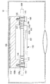
【課題】光電変換素子を簡易かつ効果的に冷却する。【解決手段】内部配線に接続されている信号用端子と前記内部配線に接続されていない固定用端子とを裏面に備える表面実装型の光電変換素子100を実装する基板109に設けられ、前記固定用端子が接合される表面側銅箔パターン104、裏面側銅箔パターン107及び、これらの銅箔パターンを接続するスルーホールビア105と、前記基板の前記裏面側銅箔パターンに固定され、該裏面側銅箔パターンを冷却する冷却部材108とを備える光電変換素子の冷却構造である。【選択図】図1A photoelectric conversion element is cooled easily and effectively. A signal processing terminal connected to an internal wiring and a fixing terminal not connected to the internal wiring are provided on a substrate on which a surface mounting type photoelectric conversion element having a back surface is mounted, and the fixing is performed. A front surface side copper foil pattern 104 to which a terminal for bonding is bonded, a back surface side copper foil pattern 107, a through hole via 105 connecting these copper foil patterns, and the back surface side copper foil pattern of the substrate fixed to the back surface It is a cooling structure of a photoelectric conversion element provided with the cooling member 108 which cools a side copper foil pattern. [Selection] Figure 1
Description
本発明は、光電変換素子の冷却構造に関するものである。 The present invention relates to a cooling structure for a photoelectric conversion element.
従来、デジタルカメラに搭載される撮像素子を実装するプリント基板に、撮像素子の裏面を露出させる貫通孔を形成し、プリント基板の裏面側に配置したヒートシンク等の冷却手段を撮像素子の裏面に直接接触させることにより、撮像素子を冷却する冷却型撮像装置が知られている(例えば、特許文献1参照)。 Conventionally, a through hole that exposes the back surface of the image sensor is formed in a printed circuit board on which the image sensor mounted on the digital camera is mounted, and a cooling means such as a heat sink disposed on the back surface side of the print circuit is directly applied to the back surface of the image sensor. A cooling-type imaging device that cools an imaging element by bringing it into contact is known (see, for example, Patent Document 1).
しかしながら、近年、撮像素子の高解像度化、高速化及び小型化が図られるに従って、裏面全体に多数の信号入出力用の端子を配置し、プリント基板に表面実装する形態の撮像素子が採用されてきており、特許文献1のようなヒートシンク等の冷却手段を直接接触させる広い面積を撮像素子の裏面に確保することができない。 However, in recent years, as the resolution, speed, and miniaturization of an image sensor have been improved, an image sensor in which a large number of signal input / output terminals are arranged on the entire back surface and mounted on the printed circuit board has been adopted. Therefore, it is impossible to secure a large area on the back surface of the image sensor in which a cooling means such as a heat sink as in Patent Document 1 is in direct contact.
このため、プリント基板に撮像素子を表面実装する場合において、撮像素子の電源端子の銅箔パターンを放熱に活用する技術が開示されている(例えば、特許文献2参照)。これは、帯状熱伝導シートを適用し帯状熱伝導シートの一方をプリント基板の銅箔パターンに、他方を金属性の枠に夫々接触させ、撮像素子を搭載したステージユニットに対して、撮像素子の放熱を実現している。ところが、帯状熱伝導シートは、放熱部材として一般に適用される金属材料に比して熱伝導率が小さいことから、充分な放熱効果が得られずSN比が低下する虞がある。また、撮像素子の電源端子の銅箔パターンを露出させるため、外乱ノイズの影響を受けやすく、何らかの衝撃によって放熱構造が崩れた場合に、電源端子とGND等において短絡が発生し、撮像素子及び周辺素子に故障をきたす虞がある。 For this reason, when surface-mounting an image pick-up element on a printed circuit board, the technique of utilizing the copper foil pattern of the power supply terminal of an image pick-up element for heat dissipation is disclosed (for example, refer patent document 2). This is because the band-shaped heat conductive sheet is applied and one of the band-shaped heat conductive sheets is brought into contact with the copper foil pattern of the printed circuit board and the other is in contact with the metallic frame, and the stage unit on which the image sensor is mounted is Realizes heat dissipation. However, the belt-like heat conductive sheet has a low thermal conductivity as compared with a metal material generally applied as a heat radiating member, so that a sufficient heat radiating effect cannot be obtained and the SN ratio may be lowered. In addition, since the copper foil pattern of the power supply terminal of the image sensor is exposed, it is easily affected by disturbance noise, and when the heat dissipation structure collapses due to some impact, a short circuit occurs between the power supply terminal and GND, etc. There is a risk of failure of the element.
本発明は、上述した事情に鑑みてなされたものであって、裏面全体に多ピンが配置された表面実装型の光電変換素子を簡易かつ効果的に冷却することができる光電変換素子の冷却構造を提供することを目的としている。 The present invention has been made in view of the circumstances described above, and is a cooling structure for a photoelectric conversion element that can easily and effectively cool a surface-mount type photoelectric conversion element in which multiple pins are arranged on the entire back surface. The purpose is to provide.
上記目的を達成するために、本発明は以下の手段を提供する。
本発明の一態様は、内部配線に接続されている信号用端子と前記内部配線に接続されていない固定用端子とを裏面に備える表面実装型の光電変換素子を実装する基板に設けられ、前記固定用端子が接合される表面側銅箔パターン、裏面側銅箔パターン及び、これらの銅箔パターンを接続するスルーホールビアと、前記基板の前記裏面側銅箔パターンに固定され、該裏面側銅箔パターンを冷却する冷却部材とを備える光電変換素子の冷却構造を提供する。
In order to achieve the above object, the present invention provides the following means.
One embodiment of the present invention is provided on a substrate on which a surface-mount photoelectric conversion element including a signal terminal connected to an internal wiring and a fixing terminal not connected to the internal wiring on a back surface is mounted, The front-side copper foil pattern, the back-side copper foil pattern to which the fixing terminals are joined, the through-hole vias that connect these copper foil patterns, and the back-side copper that is fixed to the back-side copper foil pattern of the substrate Provided is a photoelectric conversion element cooling structure including a cooling member for cooling a foil pattern.
本態様によれば、表面側銅箔パターンと裏面側銅箔パターンとを有し、両者がスルーホールビアに接続された基板において、光電変換素子がその固定用端子を表面側銅箔パターンに接合することにより実装されている。さらに、基板の裏面側に形成された裏面側銅箔パターンに冷却部材を固定する。このとき、光電変換素子の固定用端子が表面側銅箔パターンに接合され、表面側銅箔パターンと裏面側銅箔パターンとがスルーホールビアにより接続されているので、光電変換素子から生じた熱が、固定用端子、表面側銅箔パターン、スルーホールビア、裏面側銅箔パターン及び冷却部材へと順に放熱される。このように、光電変換素子から生じた熱の放熱経路を確保して、光電変換素子と冷却部材との間の熱抵抗を小さくして効率的に冷却することで、簡便な構成でかつ効果的に冷却することができる。 According to this aspect, in the substrate having the front surface side copper foil pattern and the back surface side copper foil pattern, both of which are connected to the through-hole via, the photoelectric conversion element joins the fixing terminal to the front surface side copper foil pattern. Has been implemented. Furthermore, a cooling member is fixed to the back surface side copper foil pattern formed in the back surface side of the board | substrate. At this time, the fixing terminal of the photoelectric conversion element is joined to the front side copper foil pattern, and the front side copper foil pattern and the back side copper foil pattern are connected by the through-hole via, so that the heat generated from the photoelectric conversion element However, heat is radiated sequentially to the fixing terminal, the front-side copper foil pattern, the through-hole via, the back-side copper foil pattern, and the cooling member. In this way, a heat dissipation path for the heat generated from the photoelectric conversion element is secured, and the thermal resistance between the photoelectric conversion element and the cooling member is reduced to efficiently cool, thereby having a simple configuration and effective. Can be cooled to.
上記態様においては、前記冷却部材が、前記固定用端子から、前記表面用銅箔パターン、前記スルーホールビア及び前記裏面側銅箔パターンを介して伝導されてきた熱を放散させるヒートシンクであってもよい。
このようにすることで、光電変換素子と冷却部材との間の熱抵抗を小さくして効率的に冷却し、簡便な構成でかつ効果的に冷却することができる。
In the above aspect, the cooling member may be a heat sink that dissipates heat conducted from the fixing terminal through the front surface copper foil pattern, the through-hole via, and the rear surface side copper foil pattern. Good.
By doing in this way, the thermal resistance between a photoelectric conversion element and a cooling member can be made small, and it can cool efficiently, and it can cool with a simple structure and effectively.
また、上記態様においては、前記冷却部材が、前記ヒートシンクを冷却するペルチェ素子を備えていてもよい。
このようにすることで、ペルチェ素子に電流を流すと一方の面が吸熱し、反対面は発熱する。そこで、吸熱面を裏面側銅箔パターンと接触させ、発熱面を放熱させることで、光電変換素子と冷却部材との間の熱抵抗を小さくして効率的に冷却し、簡便な構成でかつ効果的に冷却することができる。
Moreover, in the said aspect, the said cooling member may be provided with the Peltier device which cools the said heat sink.
In this way, when a current is passed through the Peltier element, one surface absorbs heat and the opposite surface generates heat. Therefore, the heat absorption surface is brought into contact with the back side copper foil pattern, and the heat generation surface is radiated to reduce the thermal resistance between the photoelectric conversion element and the cooling member, thereby efficiently cooling, and with a simple configuration and effect. Can be cooled.
また、上記態様においては、前記光電変換素子の裏面の前記信号用端子及び前記固定用端子の配置されていない領域において前記基板に貫通孔が形成され、前記ヒートシンクが、前記貫通孔を貫通して前記光電変換素子の裏面に接触する凸部を備えていてもよい。
このようにすることで、凸部が貫通孔を貫通して光電変換素子の裏面に接触するので、光電変換素子から生じた熱を直接的に冷却することができ、光電変換素子と冷却部材との間の熱抵抗を小さくして効率的に冷却し、簡便な構成でかつ効果的に冷却することができる。
Moreover, in the said aspect, a through-hole is formed in the said board | substrate in the area | region where the said signal terminal and the said fixing terminal are not arrange | positioned of the back surface of the said photoelectric conversion element, The said heat sink penetrates the said through-hole. You may provide the convex part which contacts the back surface of the said photoelectric conversion element.
By doing in this way, since a convex part penetrates a through-hole and contacts the back surface of a photoelectric conversion element, the heat generated from the photoelectric conversion element can be directly cooled, and the photoelectric conversion element, the cooling member, It is possible to cool efficiently by reducing the thermal resistance between them, and to cool effectively with a simple configuration.
また、上記態様においては、前記光電変換素子の表面の周縁部分に接触し、前記表面側銅箔パターンに固定され、前記光電変換素子の熱を前記表面側銅箔パターンに伝導する伝熱部材を備えていてもよい。
このようにすることで、光電変換素子から生じた熱が光電変換素子の表面の周縁部分に接触した伝熱部材から表面側銅箔パターンに伝導するので、放熱経路が拡大し、光電変換素子と冷却部材との間の熱抵抗を小さくして効率的に冷却し、簡便な構成でかつ効果的に冷却することができる。
Moreover, in the said aspect, the heat-transfer member which contacts the peripheral part of the surface of the said photoelectric conversion element, is fixed to the said surface side copper foil pattern, and conducts the heat | fever of the said photoelectric conversion element to the said surface side copper foil pattern. You may have.
By doing in this way, the heat generated from the photoelectric conversion element is conducted from the heat transfer member in contact with the peripheral portion of the surface of the photoelectric conversion element to the surface side copper foil pattern, so that the heat radiation path is expanded, and the photoelectric conversion element and The thermal resistance between the cooling member and the cooling member can be reduced and the cooling can be efficiently performed, and the cooling can be effectively performed with a simple configuration.
また、上記態様においては、前記光電変換素子、前記基板及び前記冷却部材を密封状態に収容する筐体を備え、前記冷却部材の放熱面が前記筐体に接触状態に配置されていてもよい。
このようにすることで、冷却部材からの熱を筐体によって効率的に放熱するので簡便な構成でかつ効果的に冷却することができる。
Moreover, in the said aspect, the housing | casing which accommodates the said photoelectric conversion element, the said board | substrate, and the said cooling member in the sealing state may be provided, and the thermal radiation surface of the said cooling member may be arrange | positioned in the said contact state.
By doing in this way, since the heat | fever from a cooling member is efficiently thermally radiated with a housing | casing, it can cool effectively with a simple structure.
また、上記態様においては、前記固定用端子が、前記光電変換素子の裏面の外周部に設けられていてもよい。
このようにすることで、光電変換素子と冷却部材との間の熱抵抗を小さくして効率的に冷却し、簡便な構成でかつ効果的に冷却することができる。
Moreover, in the said aspect, the said fixing terminal may be provided in the outer peripheral part of the back surface of the said photoelectric conversion element.
By doing in this way, the thermal resistance between a photoelectric conversion element and a cooling member can be made small, and it can cool efficiently, and it can cool with a simple structure and effectively.
また、上記態様においては、前記表面側銅箔パターンが、前記光電変換素子を前記基板に実装した状態で、前記光電変換素子の外周よりも外側に位置する領域を有していてもよい。
このようにすることで、光電変換素子と冷却部材との間の熱抵抗を小さくして効率的に冷却し、簡便な構成でかつより効果的に冷却することができる。
Moreover, in the said aspect, the said surface side copper foil pattern may have the area | region located outside the outer periphery of the said photoelectric conversion element in the state which mounted the said photoelectric conversion element in the said board | substrate.
By doing in this way, it can cool efficiently by making thermal resistance between a photoelectric conversion element and a cooling member small, and can cool more simply and more effectively.
また、上記態様においては、前記領域に設けられたスルーホールを介して、前記冷却部材を前記基板の前記裏面側銅箔パターンに固定する固定手段を備えていてもよい。
このようにすることで、さらに固定手段によって効率的に冷却し、簡便な構成でかつより効果的に冷却することができる。
Moreover, in the said aspect, you may provide the fixing means which fixes the said cooling member to the said back surface side copper foil pattern of the said board | substrate through the through hole provided in the said area | region.
By doing in this way, it can cool efficiently by a fixing means, and can be cooled more effectively with a simple structure.
本発明によれば、光電変換素子を簡易かつ効果的に冷却することができるという効果を奏する。 ADVANTAGE OF THE INVENTION According to this invention, there exists an effect that a photoelectric conversion element can be cooled simply and effectively.
(第1の実施形態)
以下、本発明の第1の実施形態に係る光電変換素子の冷却構造を適用した冷却型撮像装置について、図面を参照して以下に説明する。本実施形態において、光電変換素子としていわゆるCMOSイメージセンサ等の撮像素子を適用している。
図1及び図2に示すように、冷却型撮像装置は、冷却部材としての冷却ユニット108、プリント基板109及び撮像素子100を備え、撮像素子100の裏面にプリント基板109を介して冷却ユニット108が取り付けら、筐体放熱機構10に収容された構成となっている。
(First embodiment)
Hereinafter, a cooling type imaging apparatus to which a cooling structure for a photoelectric conversion element according to a first embodiment of the present invention is applied will be described with reference to the drawings. In the present embodiment, an imaging element such as a so-called CMOS image sensor is applied as the photoelectric conversion element.
As shown in FIGS. 1 and 2, the cooling type imaging apparatus includes a
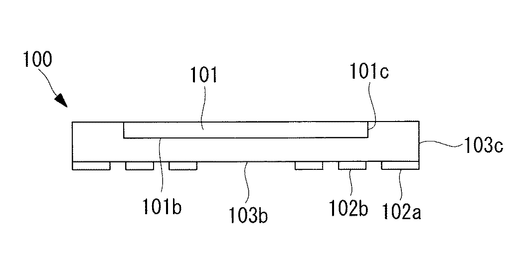
図3〜図5に示すように、撮像素子100は、例えば直方体の形状をなしており、撮像素子本体101と外装103とを備えている。撮像素子本体101は、入光面を有する本体表面101aを露出させつつ、本体裏面101b及び本体側面101cが外装103により覆われている。
As shown in FIGS. 3 to 5, the
図4に示すように、撮像素子100の裏面には、外周部(本実施形態では4隅)に設けられ、撮像素子本体101と接続されておらず撮像素子100をプリント基板109に固定するための外装空きピン102aと、中央部に設けられ、撮像素子本体101と接続された複数の外装ピン102bとが備えられている。すなわち、撮像素子100の裏面には、撮像素子100の内部配線に接続されていない固定用端子である外装空きピン102aと、撮像素子100の内部配線に接続されている信号用端子である外装ピン102bとが設けられている。
外装空きピン102a及び外装ピン102bは、外装103の裏面を貫通して外側に露出しており、外装空きピン102a及び外装ピン102bはプリント基板109に実装される際にプリント基板109に形成された銅箔パターンに接続される。
As shown in FIG. 4, the back surface of the
The exterior
外装103は、撮像素子本体101の表面101aの周縁を覆う表面外装103a、撮像素子本体101の裏面101bを覆う裏面外装103b、撮像素子本体101の側面101cを覆う側面外装103cを有している。なお、本実施形態において、裏面外装103bとは、撮像素子本体101の裏面101bにおいて、外装空きピン102a及び外装ピン102bが配置されていない領域をいう。また、図5の撮像素子100の側面図に示す通り、本実施形態に係る冷却型撮像装置に適用される撮像素子100には、プリント基板109を貫通するようなピンが存在せず、プリント基板109の表面に実装される、いわゆる表面実装型の撮像素子である。
The exterior 103 includes a
そして、図1及び図2に示すように、撮像素子100はこの外装ピン102bを用いて半田によりプリント基板109に実装される。このとき、外装空きピン102aは、プリント基板109の表面の外周部(本実施形態では4隅近傍)に形成された表面側銅箔パターン104にそれぞれ実装される。プリント基板109に設けられた銅箔パターン104は、外装空きピン102aと接触する面積よりも大きな面積を有している。
As shown in FIGS. 1 and 2, the
具体的には、図6に示すように、プリント基板109は、表面の撮像素子100の外装空きピン102aと対応する位置に、夫々矩形状の銅箔パターン104が形成されている(本実施形態では4つ)。各銅箔パターン104には、プリント基板109に実装される各種部品を電気的に接続するための複数のスルーホールビア105と、固定手段としての螺子106を取付けるためのスルーホール110とが設けられている。各銅箔パターン104は、プリント基板109に撮像素子100を実装した時に、撮像素子100の外周すなわち外装103の外周よりも外側に位置する領域を有しており、この領域にスルーホール110が位置し、撮像素子100が実装された状態でスルーホール110が露出するようになっている。なお、スルーホール110に取り付けられる螺子106は、金属など熱伝導に優れる部材からなる。
Specifically, as shown in FIG. 6, the printed
また、図7に示すように、プリント基板109の裏面には、表面側銅箔パターン104と対応する背面側銅箔パターン107が形成されている(本実施形態では4つ)。プリント基板109において、銅箔パターン104及び銅箔パターン107の基板内層は、スルーホールビア105にて複数箇所接続されている。
Further, as shown in FIG. 7, on the back surface of the printed
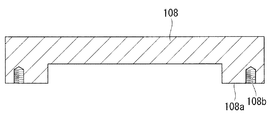
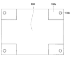
冷却ユニット108は、図8及び図9に示すように、例えば、直方体の1面の4隅から突出した脚部を有する形状とし、ヒートシンクとしての金属部材及びペルチェ素子から構成することができる。冷却ユニット108は、脚部の表面に設けられた、銅箔パターン107と接触する銅箔パターン接触面108aと、スルーホール110と対応する位置に設けられたネジ孔108bを有している。銅箔パターン接触面108aは、熱伝導グリスなどの伝熱促進部材114を介して銅箔パターン107と接触する。冷却ユニット108は、ネジ106とネジ穴108bに螺合させることにより、プリント基板109に固定される。
As shown in FIGS. 8 and 9, the
冷却ユニット108は、伝熱促進部材114を介して筐体放熱機構10と接触しており、筐体放熱機構10は密閉されている。ところで、冷却ユニット108の構成要素であるペルチェ素子は、ペルチェ効果を利用した板状の半導体素子であり、素子に電流を流すと一方の面が吸熱し、反対面は発熱する。そこで、吸熱面を背面銅箔パターン107と接触させ、発熱面を筐体放熱機構10と接触させている。
The
続いて、このように構成された冷却型撮像装置の作用について説明する。
冷却型撮像装置の電源を起動すると、冷却型撮像装置内部の図示しない駆動発生手段や設定データ書込手段によって、撮像素子100が駆動状態に移行する。撮像素子100が駆動されると、画像データを取得し画像処理手段において所定の画像処理を行った後に、表示手段等の出力装置へ画像データを出力し、画像データを出力(表示)する。
Next, the operation of the cooling type imaging apparatus configured as described above will be described.
When the power source of the cooling type imaging device is activated, the
このような駆動に際して、撮像素子100が発熱するが、冷却ユニット108が撮像素子100で発生した熱の吸熱を始める。このとき撮像素子本体101から発せられた、熱は、熱伝導、熱伝達、熱放射の3つの現象で高温部から低温部へと移動していく。撮像素子本体100の放熱経路は、撮像素子本体101から伝導し、外装ピン102bを通して基板に放熱する経路(熱伝導)と、表面から空気に放熱する経路(熱伝達、熱放射)があり、熱は熱抵抗の小さい箇所から移動していく。熱抵抗は、以下の式1で求められる。
During such driving, the
上記式1によれば、熱伝導の経路において、長さが短く、熱伝導率・幅・厚さ(=面積)が大きい方が熱抵抗は小さくなる。 According to the above formula 1, in the heat conduction path, the shorter the length and the larger the heat conductivity / width / thickness (= area), the smaller the thermal resistance.
冷却型撮像装置に適用し得る物質の熱伝導率について、下記表1に示す。
上記表1より、熱伝導率については、銅やアルミニウム、半田などの金属が高く、エポキシや空気は低いことが分かる。よって、撮像素子100の放熱経路は、熱伝導率、部品表面積、密閉内部空気の流体移動の観点から、プリント基板109からの放熱経路が支配的である。これは、撮像素子100の外装103と空気の間の熱抵抗よりも、電極(外装空きピン102a,外装ピン102b)とプリント基板109間の熱抵抗の方が圧倒的に低いためである。
From Table 1 above, it can be seen that the thermal conductivity is high for metals such as copper, aluminum and solder, and low for epoxy and air. Therefore, the heat dissipation path of the
ここで、撮像素子100の支配的な放熱経路となるプリント基板109を構成する材料のうち、主材料である銅とエポキシ(FR4)の熱抵抗[℃/W]を示す。
Here, the thermal resistance [° C./W] of copper and epoxy (FR4), which are the main materials, of the materials constituting the printed
銅
横方向(厚さ=0.035mm):79[℃/W]
厚さ方向(厚さ=0.035mm(2.54cm^2)):0.00015[℃/W]
スルーホールビア1個(φ0.5mm、高さ1.5mm):100[℃/W]
スルーホールビアビアN個:100/N[℃/W]
Copper lateral direction (thickness = 0.035 mm): 79 [° C./W]
Thickness direction (thickness = 0.035 mm (2.54 cm ^ 2)): 0.00015 [° C./W]
One through-hole via (φ0.5 mm, height 1.5 mm): 100 [° C./W]
N through-hole vias: 100 / N [° C / W]
エポキシ(FR4)
横方向(厚さ=1.5mm):2699[℃/W]
厚さ方向(厚さ=1.5mm(2.54cm^2)):9.3[℃/W]
Epoxy (FR4)
Lateral direction (thickness = 1.5 mm): 2699 [° C./W]
Thickness direction (thickness = 1.5 mm (2.54 cm ^ 2)): 9.3 [° C./W]
つまり、プリント基板109の面にそって横方向に熱を逃がす場合で比較すると、銅の方が熱伝導性に優れている。また、基板の厚さ方向に熱を逃がす場合は、エポキシ(FR4)を経由し、銅箔パターンにおいてスルーホールビアを複数設けることで熱抵抗を小さくし、熱伝導性を向上することができる。
That is, compared with the case where heat is released in the lateral direction along the surface of the printed
通常の銅箔パターンの大きさは、外装空きピン102aのサイズと同程度であるためエポキシ(FR4)の面積が多く、プリント基板109の横方向の熱伝導は期待できない。プリント基板109の厚さ方向においても、スルーホールビアを複数設置することやエポキシ(FP4)を介して熱抵抗は小さくなるが、金属などの熱伝導に優れる部材には劣る。
Since the size of the normal copper foil pattern is almost the same as the size of the exterior
本実施形態においては、撮像素子100の外装空きピン102aに対し、プリント基板109の横方向の熱伝導を向上させるために熱伝導に優れる銅箔パターン104、銅箔パターン107を撮像素子100の実装面積を超える程度に拡大させて設けている。またプリント基板109の基板厚さ方向の熱伝導を向上させるために、複数のスルーホールビア105で両銅箔パターン104,107をプリント基板109の内層で接続し、かつ熱伝導性に優れる部材で構成される固定手段としての螺子106を、両銅箔パターン104,107に設けたスルーホール110を介して設置する構成となっている。
In the present embodiment, the
螺子106は、上記表1に記載した銅やアルミニウムなどエポキシと比較して熱伝導率の高い物質で構成されるため、熱抵抗が小さく螺子106による熱伝導も発生する。従って、プリント基板109に実装された発熱体である撮像素子100と、吸熱を行う冷却ユニット108と接触する銅箔パターン107との間の熱抵抗は小さくなっている。
Since the
冷却ユニット108は、螺子106によって伝熱促進部材114を介して面精度良く銅箔パターン107と接続されているため、撮像素子100と冷却ユニット108との間の熱抵抗が小さく、撮像素子100の冷却を行うことができる。
冷却ユニット108が吸熱した熱の放熱は、冷却ユニット108の放熱面と伝熱促進部材114を介して接触した筐体放熱機構10によって行われる。筐体放熱機構10は、十分な表面積を有し、熱を外部の空気へと放熱する。
Since the
The heat dissipated by the
このように、冷却ユニット108と撮像素子100との間の熱抵抗を小さくし、冷却ユニット108を用いて撮像素子100を冷却することで、簡便な構成でかつ効果的に冷却することができ、SN比の良好な画像を取得することができる。
Thus, by reducing the thermal resistance between the cooling
(第2の実施形態)
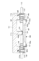
本実施形態にかかる冷却型撮像装置は、上記した第1の実施形態と略同様の構成あり、プリント基板109に代えて開口部118を有するプリント基板112を適用すると共に、冷却ユニット108に代えて凸部111cを有する凸型冷却ユニット111を適用することにより、撮像素子100に対してプリント基板112を介さずに直接接触させて冷却する構成となっている。
(Second Embodiment)
The cooling type imaging apparatus according to the present embodiment has substantially the same configuration as that of the first embodiment described above, and applies a printed
なお、本実施形態に係る冷却型撮像装置において第1の実施形態に係る冷却型撮像装置と同一の構成には同符号を付し、その説明を省略する。また、本実施形態に係る冷却型撮像装置も筐体放熱機構に収容されるものであるが、その説明を省略する。以下、上記した第1の実施形態に係る冷却型撮像装置との相違点についてのみ説明する。 Note that, in the cooling type imaging apparatus according to the present embodiment, the same components as those in the cooling type imaging apparatus according to the first embodiment are denoted by the same reference numerals, and description thereof is omitted. In addition, the cooling type imaging apparatus according to the present embodiment is also housed in the case heat dissipation mechanism, but the description thereof is omitted. Hereinafter, only differences from the above-described cooling type imaging apparatus according to the first embodiment will be described.
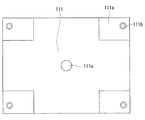
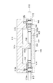
図10〜図12に示すように、プリント基板112には、その中心部分に開口部118が設けられている。また、凸型冷却ユニット111には、開口部118との対峙する位置に凸部111cが設けられている。これにより、撮像素子100に対して凸型冷却ユニット111を、プリント基板112を介さずに直接的に接触させて冷却することができる。
As shown in FIGS. 10 to 12, the printed
撮像素子100は、格子状に撮像素子本体101と内層で接続された外装ピン102bの先端及び外装空きピン102aの先端が、撮像素子100の裏面すなわち裏面外装103bの裏面から露出して配置されている。特に、撮像素子100の裏面の中央部付近には、プリント基板112の開口部118と対向する位置に外装ピン102bが存在しない領域が設けられている。従って、図12に示すように、プリント基板112と撮像素子100とを取り付けた状態で裏面を正面視すると、プリント基板112の開口部118から撮像素子100の裏面外装103bが露出するようになっている。
The
図10、図13及び図14において、凸型冷却ユニット111には、プリント基板112の開口部118と対向する位置に凸部111cが設けられている。凸型冷却ユニット111が螺子106によりプリント基板112にと取付けられた際に、凸部111cの先端がプリント基板112の開口部118を貫通し、撮像素子100の裏面外装103bに直接接触するようになっている。ここで、凸部111cは、凸型冷却ユニット111の部品精度や螺子106の固定の程度によって、撮像素子100の裏面外装103bと非接触になってしまう虞がある。また凸部111cが強く接触することで圧力が生じ、撮像素子100の裏面外装103b付近の外装ピン102bによる半田剥がれ等が生じる虞がある。
10, 13, and 14, the
そこで、凸型冷却ユニット111について、凸部111cを銅箔パターン接触面111aに対しては高く形成すると共に、銅箔パターン接触面111aとの高さの差分がプリント基板112の厚みよりも小さくなるように精度よく構成する。凸部111cの凸部の銅箔パターン接触面111aとの高さの差分を、プリント基板112の厚みよりも小さくすることで、凸部111cと裏面外装103bとの間に微小な隙間が発生する。この生じた隙間に伝熱促進部材114を充填することで部材の物理的な接触を防止することによる半田剥がれを防止すると共に、非接触となることを防止して熱伝導が確実に行われるようにして放熱経路を確保している。
Therefore, in the
本実施形態において、外装103と凸型冷却ユニット111の間は、伝熱促進部材114を介して直接接触させることにより、その熱抵抗を小さくすることができる。特に、直接接触不可状態である撮像素子外装103と空気の間の熱抵抗と比較すると圧倒的に熱抵抗は小さくなる。熱抵抗の小さい箇所が増加したことで、撮像素子100の放熱経路が、上記した第1の実施形態で述べた銅箔パターンのみに限らず、本実施例の凸型冷却ユニット111の接触箇所も併用することで増加したため、撮像素子100の冷却をより効率的に行うことでできる。
In the present embodiment, the thermal resistance can be reduced by bringing the
このように、凸型冷却ユニット111に凸部118を設けることで、凸型冷却ユニット111と撮像素子100との間の熱抵抗をより小さくているので、凸型冷却ユニット111を用いて撮像素子100を冷却することで、簡便な構成でかつ効果的に冷却することができ、SN比の良好な画像を取得することができる。
As described above, since the
(第3の実施形態)
第3の実施形態に係る冷却型撮像装置は、放熱部材117を有しており、この放熱部材117が銅箔パターン104又は伝熱促進部材114を介して撮像素子100に接触し、螺子106により固定されて撮像素子100を冷却するようになっている。本実施形態においても、第1及び第2の実施形態に係る冷却型撮像装置と同一の構成には同一の符号を付し、その説明を省略する。
(Third embodiment)
The cooling type imaging apparatus according to the third embodiment includes a
図15〜図17に示すように、本実施形態に係る撮像素子100は、直方体の形状を成し、入光面である表面101aの周縁、裏面101b及び側面101cを外装103によって覆い、保護している。撮像素子100からの発熱をより効果的に放熱するために、表面外装103a及び側面外装103cを覆い、かつ、接触するように放熱部材117を配置する。
As shown in FIGS. 15 to 17, the
放熱部材117は、撮像素子100の表面101aの入光面に被らず、かつ撮像素子100の外装103を覆うように可能な限り撮像素子100と接触する面積が大きくなるように配置する。また、放熱部材117は、銅箔パターン104をも覆うように配置する。さらに、放熱部材117と撮像素子100との接触箇所には、伝熱促進部材114を塗布している。従って、放熱部材117は、伝熱促進部材114を介して銅箔パターン104と間接的に接触し、螺子106によって固定される。
The
このように、凸型冷却ユニット111が、その凸部111cにより外装103と直接的に接触し、かつ、伝熱促進部材114及び螺子106を介して放熱部材117と接触することで、上述した他の実施形態に係る冷却型撮像装置に比して、凸型冷却ユニット111と撮像素子100との接触面積が大きくなる。
As described above, the
つまり、裏面外装103bのみならず、表面外装103a及び側面外装103cも熱伝導を用いた放熱経路として活用することにより、撮像素子100の放熱経路を複数形成することができ、撮像素子100の冷却をより効率的に行うことでできる。よって、凸型冷却ユニット111と撮像素子100との間の熱抵抗を小さくし、凸型冷却ユニット111を用いて撮像素子100を冷却することで、S/Nの良い画像を取得することができる。
That is, not only the
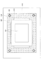
なお、プリント基板開口部118は、熱伝導を向上させるためにスルーホールにしても良い。また、放熱のための銅箔パターン107は、上記した各実施形態に示すものに限られず、例えば図18乃至図20に示すように撮像素子100の周囲を囲繞するように、可能な限り大きな面積となるようにすることもできる。
なお、各実施形態では、図2、図10、図15及び図18に示すように、冷却ユニットとプリント基板との間に空間を設けているが、これに限られず、この空間に伝熱促進部材114を充填しても良い。
このように、冷却ユニットとプリント基板との間にも伝熱促進部材114を充填することで、空気と比較して熱伝導が向上し、より撮像素子100を効率的に冷却することができる。
The printed
In each embodiment, as shown in FIGS. 2, 10, 15, and 18, a space is provided between the cooling unit and the printed board. However, the present invention is not limited to this, and heat transfer is promoted in this space. The
Thus, by filling the heat
10 筐体放熱機構
100 撮像素子
101 撮像素子本体
101a 表面
101b 裏面
101c 側面
102a 外装空きピン
102b 外装ピン
103 外装
103a 表面外装
103b 裏面外装
103c 側面外装
104 表面側銅箔パターン
105 スルーホールビア
106 螺子(固定手段)
107 背面側銅箔パターン
108 冷却ユニット
108a 銅箔パターン接触面
108b ネジ孔
109 プリント基板
110 スルーホール
111 凸型冷却ユニット
111a 銅箔パターン接触面
111b ネジ孔
111c 凸部
112 プリント基板
113 銅箔パターン
114 伝熱促進部材
115 銅箔パターン
116 プリント基板
117 放熱部材
118 開口部
DESCRIPTION OF
107 Back side
Claims (9)
前記基板の前記裏面側銅箔パターンに固定され、該裏面側銅箔パターンを冷却する冷却部材とを備える光電変換素子の冷却構造。 Provided on a substrate on which a surface mounting type photoelectric conversion element having a signal terminal connected to internal wiring and a fixing terminal not connected to the internal wiring on the back surface is mounted, and the fixing terminal is joined Front side copper foil pattern, back side copper foil pattern, and through-hole vias connecting these copper foil patterns,
The cooling structure of a photoelectric conversion element provided with the cooling member fixed to the said back surface side copper foil pattern of the said board | substrate, and cooling this back surface side copper foil pattern.
光電変換素子の冷却構造。 The cooling structure for a photoelectric conversion element according to claim 2, wherein the cooling member includes a Peltier element for cooling the heat sink.
前記ヒートシンクが、前記貫通孔を貫通して前記光電変換素子の裏面に接触する凸部を備える請求項2または請求項3に記載の光電変換素子の冷却構造。 A through hole is formed in the substrate in a region where the signal terminal and the fixing terminal are not arranged on the back surface of the photoelectric conversion element,
The cooling structure of the photoelectric conversion element according to claim 2, wherein the heat sink includes a convex portion that penetrates the through hole and contacts the back surface of the photoelectric conversion element.
前記冷却部材の放熱面が前記筐体に接触状態に配置されている請求項1から請求項5のいずれかに記載の光電変換素子の冷却構造。 A housing that houses the photoelectric conversion element, the substrate, and the cooling member in a sealed state;
The cooling structure for a photoelectric conversion element according to claim 1, wherein a heat radiation surface of the cooling member is disposed in contact with the housing.
Priority Applications (3)
| Application Number | Priority Date | Filing Date | Title |
|---|---|---|---|
| JP2015116610A JP6588243B2 (en) | 2015-06-09 | 2015-06-09 | Cooling structure of photoelectric conversion element |
| US15/148,129 US10020407B2 (en) | 2015-06-09 | 2016-05-06 | Cooling structure for photoelectric conversion element |
| EP16169322.1A EP3118899B1 (en) | 2015-06-09 | 2016-05-12 | Cooling structure for photoelectric conversion element |
Applications Claiming Priority (1)
| Application Number | Priority Date | Filing Date | Title |
|---|---|---|---|
| JP2015116610A JP6588243B2 (en) | 2015-06-09 | 2015-06-09 | Cooling structure of photoelectric conversion element |
Publications (2)
| Publication Number | Publication Date |
|---|---|
| JP2017005455A true JP2017005455A (en) | 2017-01-05 |
| JP6588243B2 JP6588243B2 (en) | 2019-10-09 |
Family
ID=55970857
Family Applications (1)
| Application Number | Title | Priority Date | Filing Date |
|---|---|---|---|
| JP2015116610A Active JP6588243B2 (en) | 2015-06-09 | 2015-06-09 | Cooling structure of photoelectric conversion element |
Country Status (3)
| Country | Link |
|---|---|
| US (1) | US10020407B2 (en) |
| EP (1) | EP3118899B1 (en) |
| JP (1) | JP6588243B2 (en) |
Cited By (4)
| Publication number | Priority date | Publication date | Assignee | Title |
|---|---|---|---|---|
| WO2019119365A1 (en) * | 2017-12-21 | 2019-06-27 | 深圳市大疆创新科技有限公司 | Camera, photographing device and unmanned aerial vehicle |
| JP2021141297A (en) * | 2020-03-10 | 2021-09-16 | ロベルト・ボッシュ・ゲゼルシャフト・ミト・ベシュレンクテル・ハフツングRobert Bosch Gmbh | Electronic control unit |
| WO2024161983A1 (en) * | 2023-02-03 | 2024-08-08 | i-PRO株式会社 | Imaging device |
| KR20250030239A (en) * | 2023-08-24 | 2025-03-05 | 삼성전기주식회사 | Camera Module |
Families Citing this family (4)
| Publication number | Priority date | Publication date | Assignee | Title |
|---|---|---|---|---|
| DE102017126531A1 (en) * | 2017-11-13 | 2019-05-16 | Connaught Electronics Ltd. | Camera for a motor vehicle, in a deformable thermally conductive medium is inserted into a screw connection, as well as method |
| DE102019119118B4 (en) | 2019-07-15 | 2024-06-13 | Infineon Technologies Ag | SEMICONDUCTOR HOUSING, SEMICONDUCTOR ARRANGEMENT AND METHOD FOR PRODUCING A SEMICONDUCTOR HOUSING |
| CN110620869A (en) * | 2019-10-29 | 2019-12-27 | 维沃移动通信有限公司 | Camera module and electronic equipment |
| FR3136110B1 (en) * | 2022-05-25 | 2025-06-20 | 3D Plus | Thermal drainage part of a 3D electronic module |
Citations (2)
| Publication number | Priority date | Publication date | Assignee | Title |
|---|---|---|---|---|
| JP2010233015A (en) * | 2009-03-27 | 2010-10-14 | Canon Inc | Imaging device |
| US20140291790A1 (en) * | 2013-04-01 | 2014-10-02 | Industrial Technology Research Institute | Encapsulation of backside illumination photosensitive device |
Family Cites Families (16)
| Publication number | Priority date | Publication date | Assignee | Title |
|---|---|---|---|---|
| US5625227A (en) * | 1995-01-18 | 1997-04-29 | Dell Usa, L.P. | Circuit board-mounted IC package cooling apparatus |
| JP2803603B2 (en) | 1995-09-18 | 1998-09-24 | 日本電気株式会社 | Multi-chip package structure |
| JPH09289329A (en) | 1996-04-22 | 1997-11-04 | Fujitsu Ltd | Electronic circuit module |
| JP2000269671A (en) * | 1999-03-19 | 2000-09-29 | Toshiba Corp | Electronics |
| US6654250B1 (en) * | 2002-09-25 | 2003-11-25 | International Business Machines Corporation | Low-stress compressive heatsink structure |
| US20040238947A1 (en) * | 2003-05-28 | 2004-12-02 | Intel Corporation | Package and method for attaching an integrated heat spreader |
| US6870258B1 (en) * | 2003-06-16 | 2005-03-22 | Advanced Micro Devices | Fixture suitable for use in coupling a lid to a substrate and method |
| WO2009111874A1 (en) * | 2008-03-11 | 2009-09-17 | The Royal Institution For The Advancement Of Learning/ Mcgiil University | Low-temperature wafer level processing for mems devices |
| JP2010225919A (en) | 2009-03-24 | 2010-10-07 | Sony Corp | Semiconductor device |
| DE102009026558B3 (en) * | 2009-05-28 | 2010-12-02 | Infineon Technologies Ag | Power semiconductor module with movably mounted circuit carriers and method for producing such a power semiconductor module |
| JP2011120044A (en) | 2009-12-04 | 2011-06-16 | Nikon Corp | Cooling type imaging apparatus |
| JP5371106B2 (en) | 2009-12-04 | 2013-12-18 | 富士機械製造株式会社 | Heat dissipation structure for image sensor package |
| JP2012085024A (en) | 2010-10-08 | 2012-04-26 | Casio Comput Co Ltd | Mounting structure and image pick-up device with mounting structure |
| CN104583675A (en) * | 2012-09-03 | 2015-04-29 | 夏普株式会社 | Lighting apparatus, display apparatus, and television receiver |
| US9024429B2 (en) * | 2013-08-29 | 2015-05-05 | Freescale Semiconductor Inc. | Microelectronic packages containing opposing devices and methods for the fabrication thereof |
| US9258465B2 (en) * | 2014-01-09 | 2016-02-09 | Omnivision Technologies, Inc. | Image device having efficient heat transfer, and associated systems |
-
2015
- 2015-06-09 JP JP2015116610A patent/JP6588243B2/en active Active
-
2016
- 2016-05-06 US US15/148,129 patent/US10020407B2/en active Active
- 2016-05-12 EP EP16169322.1A patent/EP3118899B1/en active Active
Patent Citations (2)
| Publication number | Priority date | Publication date | Assignee | Title |
|---|---|---|---|---|
| JP2010233015A (en) * | 2009-03-27 | 2010-10-14 | Canon Inc | Imaging device |
| US20140291790A1 (en) * | 2013-04-01 | 2014-10-02 | Industrial Technology Research Institute | Encapsulation of backside illumination photosensitive device |
Cited By (6)
| Publication number | Priority date | Publication date | Assignee | Title |
|---|---|---|---|---|
| WO2019119365A1 (en) * | 2017-12-21 | 2019-06-27 | 深圳市大疆创新科技有限公司 | Camera, photographing device and unmanned aerial vehicle |
| JP2021141297A (en) * | 2020-03-10 | 2021-09-16 | ロベルト・ボッシュ・ゲゼルシャフト・ミト・ベシュレンクテル・ハフツングRobert Bosch Gmbh | Electronic control unit |
| JP7537889B2 (en) | 2020-03-10 | 2024-08-21 | ロベルト・ボッシュ・ゲゼルシャフト・ミト・ベシュレンクテル・ハフツング | Electronic Control Unit |
| WO2024161983A1 (en) * | 2023-02-03 | 2024-08-08 | i-PRO株式会社 | Imaging device |
| KR20250030239A (en) * | 2023-08-24 | 2025-03-05 | 삼성전기주식회사 | Camera Module |
| KR102881454B1 (en) * | 2023-08-24 | 2025-11-04 | 삼성전기주식회사 | Camera Module |
Also Published As
| Publication number | Publication date |
|---|---|
| US10020407B2 (en) | 2018-07-10 |
| JP6588243B2 (en) | 2019-10-09 |
| EP3118899B1 (en) | 2018-10-10 |
| US20160365461A1 (en) | 2016-12-15 |
| EP3118899A1 (en) | 2017-01-18 |
Similar Documents
| Publication | Publication Date | Title |
|---|---|---|
| JP6588243B2 (en) | Cooling structure of photoelectric conversion element | |
| JP5371106B2 (en) | Heat dissipation structure for image sensor package | |
| KR20180016799A (en) | Printed circuit board assembly | |
| JP6315229B2 (en) | Heat dissipation parts, electronic equipment | |
| WO2017022221A1 (en) | Heat dissipating structure and electronic apparatus | |
| JP2008235775A (en) | High frequency module | |
| JP5169800B2 (en) | Electronic equipment | |
| TW201215302A (en) | Thermal module and electronic device incorporating the same | |
| JP2016024334A (en) | Display device | |
| JP2006191465A (en) | Electronics | |
| JP2014000314A (en) | Heat radiation structure of endoscope distal end | |
| JP2008227653A (en) | Semiconductor device having imaging element | |
| JP2013065887A (en) | Electronic device | |
| JP2010182792A (en) | Electronic circuit device | |
| JP2020108004A (en) | Electronic device heat dissipation structure and heat dissipation method | |
| KR20160036945A (en) | Printed circuit board and electronic component package having the same | |
| JP2009059760A (en) | Electronic circuit board heat dissipation structure | |
| JP6686467B2 (en) | Electronic component heat dissipation structure | |
| JP2017162860A (en) | Electronic control unit | |
| JP2007158779A (en) | Camera module heat dissipation device | |
| JP6088461B2 (en) | Heat dissipation structure of control device | |
| JP2006054318A (en) | Electric component module and its manufacturing method | |
| JP2005057149A (en) | Electric component module and its manufacturing method | |
| JP2006186483A (en) | Imaging unit and heat dissipation structure of imaging element | |
| JP2013172168A (en) | Heat dissipation device, and imaging apparatus |
Legal Events
| Date | Code | Title | Description |
|---|---|---|---|
| A621 | Written request for application examination |
Free format text: JAPANESE INTERMEDIATE CODE: A621 Effective date: 20180405 |
|
| A977 | Report on retrieval |
Free format text: JAPANESE INTERMEDIATE CODE: A971007 Effective date: 20190208 |
|
| A131 | Notification of reasons for refusal |
Free format text: JAPANESE INTERMEDIATE CODE: A131 Effective date: 20190326 |
|
| A521 | Request for written amendment filed |
Free format text: JAPANESE INTERMEDIATE CODE: A523 Effective date: 20190509 |
|
| TRDD | Decision of grant or rejection written | ||
| A01 | Written decision to grant a patent or to grant a registration (utility model) |
Free format text: JAPANESE INTERMEDIATE CODE: A01 Effective date: 20190903 |
|
| A61 | First payment of annual fees (during grant procedure) |
Free format text: JAPANESE INTERMEDIATE CODE: A61 Effective date: 20190912 |
|
| R151 | Written notification of patent or utility model registration |
Ref document number: 6588243 Country of ref document: JP Free format text: JAPANESE INTERMEDIATE CODE: R151 |
|
| R250 | Receipt of annual fees |
Free format text: JAPANESE INTERMEDIATE CODE: R250 |
|
| S111 | Request for change of ownership or part of ownership |
Free format text: JAPANESE INTERMEDIATE CODE: R313111 |
|
| R371 | Transfer withdrawn |
Free format text: JAPANESE INTERMEDIATE CODE: R371 |
|
| S111 | Request for change of ownership or part of ownership |
Free format text: JAPANESE INTERMEDIATE CODE: R313111 |
|
| R350 | Written notification of registration of transfer |
Free format text: JAPANESE INTERMEDIATE CODE: R350 |
|
| R250 | Receipt of annual fees |
Free format text: JAPANESE INTERMEDIATE CODE: R250 |
|
| R250 | Receipt of annual fees |
Free format text: JAPANESE INTERMEDIATE CODE: R250 |
|
| R250 | Receipt of annual fees |
Free format text: JAPANESE INTERMEDIATE CODE: R250 |