JP2017010512A - Calculation control indicator cache - Google Patents
Calculation control indicator cache Download PDFInfo
- Publication number
- JP2017010512A JP2017010512A JP2015227713A JP2015227713A JP2017010512A JP 2017010512 A JP2017010512 A JP 2017010512A JP 2015227713 A JP2015227713 A JP 2015227713A JP 2015227713 A JP2015227713 A JP 2015227713A JP 2017010512 A JP2017010512 A JP 2017010512A
- Authority
- JP
- Japan
- Prior art keywords
- rounding
- result
- microprocessor
- instruction execution
- intermediate result
- Prior art date
- Legal status (The legal status is an assumption and is not a legal conclusion. Google has not performed a legal analysis and makes no representation as to the accuracy of the status listed.)
- Granted
Links
Images






Classifications
-
- G—PHYSICS
- G06—COMPUTING OR CALCULATING; COUNTING
- G06F—ELECTRIC DIGITAL DATA PROCESSING
- G06F7/00—Methods or arrangements for processing data by operating upon the order or content of the data handled
- G06F7/38—Methods or arrangements for performing computations using exclusively denominational number representation, e.g. using binary, ternary, decimal representation
- G06F7/48—Methods or arrangements for performing computations using exclusively denominational number representation, e.g. using binary, ternary, decimal representation using non-contact-making devices, e.g. tube, solid state device; using unspecified devices
- G06F7/483—Computations with numbers represented by a non-linear combination of denominational numbers, e.g. rational numbers, logarithmic number system or floating-point numbers
-
- G—PHYSICS
- G06—COMPUTING OR CALCULATING; COUNTING
- G06F—ELECTRIC DIGITAL DATA PROCESSING
- G06F17/00—Digital computing or data processing equipment or methods, specially adapted for specific functions
- G06F17/10—Complex mathematical operations
- G06F17/16—Matrix or vector computation, e.g. matrix-matrix or matrix-vector multiplication, matrix factorization
-
- G—PHYSICS
- G06—COMPUTING OR CALCULATING; COUNTING
- G06F—ELECTRIC DIGITAL DATA PROCESSING
- G06F7/00—Methods or arrangements for processing data by operating upon the order or content of the data handled
- G06F7/38—Methods or arrangements for performing computations using exclusively denominational number representation, e.g. using binary, ternary, decimal representation
- G06F7/48—Methods or arrangements for performing computations using exclusively denominational number representation, e.g. using binary, ternary, decimal representation using non-contact-making devices, e.g. tube, solid state device; using unspecified devices
- G06F7/483—Computations with numbers represented by a non-linear combination of denominational numbers, e.g. rational numbers, logarithmic number system or floating-point numbers
- G06F7/487—Multiplying; Dividing
- G06F7/4876—Multiplying
-
- G—PHYSICS
- G06—COMPUTING OR CALCULATING; COUNTING
- G06F—ELECTRIC DIGITAL DATA PROCESSING
- G06F7/00—Methods or arrangements for processing data by operating upon the order or content of the data handled
- G06F7/38—Methods or arrangements for performing computations using exclusively denominational number representation, e.g. using binary, ternary, decimal representation
- G06F7/48—Methods or arrangements for performing computations using exclusively denominational number representation, e.g. using binary, ternary, decimal representation using non-contact-making devices, e.g. tube, solid state device; using unspecified devices
- G06F7/499—Denomination or exception handling, e.g. rounding or overflow
-
- G—PHYSICS
- G06—COMPUTING OR CALCULATING; COUNTING
- G06F—ELECTRIC DIGITAL DATA PROCESSING
- G06F7/00—Methods or arrangements for processing data by operating upon the order or content of the data handled
- G06F7/38—Methods or arrangements for performing computations using exclusively denominational number representation, e.g. using binary, ternary, decimal representation
- G06F7/48—Methods or arrangements for performing computations using exclusively denominational number representation, e.g. using binary, ternary, decimal representation using non-contact-making devices, e.g. tube, solid state device; using unspecified devices
- G06F7/499—Denomination or exception handling, e.g. rounding or overflow
- G06F7/49905—Exception handling
- G06F7/4991—Overflow or underflow
- G06F7/49915—Mantissa overflow or underflow in handling floating-point numbers
-
- G—PHYSICS
- G06—COMPUTING OR CALCULATING; COUNTING
- G06F—ELECTRIC DIGITAL DATA PROCESSING
- G06F7/00—Methods or arrangements for processing data by operating upon the order or content of the data handled
- G06F7/38—Methods or arrangements for performing computations using exclusively denominational number representation, e.g. using binary, ternary, decimal representation
- G06F7/48—Methods or arrangements for performing computations using exclusively denominational number representation, e.g. using binary, ternary, decimal representation using non-contact-making devices, e.g. tube, solid state device; using unspecified devices
- G06F7/499—Denomination or exception handling, e.g. rounding or overflow
- G06F7/49942—Significance control
- G06F7/49947—Rounding
- G06F7/49957—Implementation of IEEE-754 Standard
-
- G—PHYSICS
- G06—COMPUTING OR CALCULATING; COUNTING
- G06F—ELECTRIC DIGITAL DATA PROCESSING
- G06F7/00—Methods or arrangements for processing data by operating upon the order or content of the data handled
- G06F7/38—Methods or arrangements for performing computations using exclusively denominational number representation, e.g. using binary, ternary, decimal representation
- G06F7/48—Methods or arrangements for performing computations using exclusively denominational number representation, e.g. using binary, ternary, decimal representation using non-contact-making devices, e.g. tube, solid state device; using unspecified devices
- G06F7/544—Methods or arrangements for performing computations using exclusively denominational number representation, e.g. using binary, ternary, decimal representation using non-contact-making devices, e.g. tube, solid state device; using unspecified devices for evaluating functions by calculation
-
- G—PHYSICS
- G06—COMPUTING OR CALCULATING; COUNTING
- G06F—ELECTRIC DIGITAL DATA PROCESSING
- G06F7/00—Methods or arrangements for processing data by operating upon the order or content of the data handled
- G06F7/38—Methods or arrangements for performing computations using exclusively denominational number representation, e.g. using binary, ternary, decimal representation
- G06F7/48—Methods or arrangements for performing computations using exclusively denominational number representation, e.g. using binary, ternary, decimal representation using non-contact-making devices, e.g. tube, solid state device; using unspecified devices
- G06F7/544—Methods or arrangements for performing computations using exclusively denominational number representation, e.g. using binary, ternary, decimal representation using non-contact-making devices, e.g. tube, solid state device; using unspecified devices for evaluating functions by calculation
- G06F7/5443—Sum of products
-
- G—PHYSICS
- G06—COMPUTING OR CALCULATING; COUNTING
- G06F—ELECTRIC DIGITAL DATA PROCESSING
- G06F9/00—Arrangements for program control, e.g. control units
- G06F9/06—Arrangements for program control, e.g. control units using stored programs, i.e. using an internal store of processing equipment to receive or retain programs
- G06F9/22—Microcontrol or microprogram arrangements
- G06F9/223—Execution means for microinstructions irrespective of the microinstruction function, e.g. decoding of microinstructions and nanoinstructions; timing of microinstructions; programmable logic arrays; delays and fan-out problems
-
- G—PHYSICS
- G06—COMPUTING OR CALCULATING; COUNTING
- G06F—ELECTRIC DIGITAL DATA PROCESSING
- G06F9/00—Arrangements for program control, e.g. control units
- G06F9/06—Arrangements for program control, e.g. control units using stored programs, i.e. using an internal store of processing equipment to receive or retain programs
- G06F9/30—Arrangements for executing machine instructions, e.g. instruction decode
-
- G—PHYSICS
- G06—COMPUTING OR CALCULATING; COUNTING
- G06F—ELECTRIC DIGITAL DATA PROCESSING
- G06F9/00—Arrangements for program control, e.g. control units
- G06F9/06—Arrangements for program control, e.g. control units using stored programs, i.e. using an internal store of processing equipment to receive or retain programs
- G06F9/30—Arrangements for executing machine instructions, e.g. instruction decode
- G06F9/30003—Arrangements for executing specific machine instructions
- G06F9/30007—Arrangements for executing specific machine instructions to perform operations on data operands
- G06F9/3001—Arithmetic instructions
-
- G—PHYSICS
- G06—COMPUTING OR CALCULATING; COUNTING
- G06F—ELECTRIC DIGITAL DATA PROCESSING
- G06F9/00—Arrangements for program control, e.g. control units
- G06F9/06—Arrangements for program control, e.g. control units using stored programs, i.e. using an internal store of processing equipment to receive or retain programs
- G06F9/30—Arrangements for executing machine instructions, e.g. instruction decode
- G06F9/30003—Arrangements for executing specific machine instructions
- G06F9/30007—Arrangements for executing specific machine instructions to perform operations on data operands
- G06F9/3001—Arithmetic instructions
- G06F9/30014—Arithmetic instructions with variable precision
-
- G—PHYSICS
- G06—COMPUTING OR CALCULATING; COUNTING
- G06F—ELECTRIC DIGITAL DATA PROCESSING
- G06F9/00—Arrangements for program control, e.g. control units
- G06F9/06—Arrangements for program control, e.g. control units using stored programs, i.e. using an internal store of processing equipment to receive or retain programs
- G06F9/30—Arrangements for executing machine instructions, e.g. instruction decode
- G06F9/30145—Instruction analysis, e.g. decoding, instruction word fields
-
- G—PHYSICS
- G06—COMPUTING OR CALCULATING; COUNTING
- G06F—ELECTRIC DIGITAL DATA PROCESSING
- G06F9/00—Arrangements for program control, e.g. control units
- G06F9/06—Arrangements for program control, e.g. control units using stored programs, i.e. using an internal store of processing equipment to receive or retain programs
- G06F9/30—Arrangements for executing machine instructions, e.g. instruction decode
- G06F9/3017—Runtime instruction translation, e.g. macros
-
- G—PHYSICS
- G06—COMPUTING OR CALCULATING; COUNTING
- G06F—ELECTRIC DIGITAL DATA PROCESSING
- G06F9/00—Arrangements for program control, e.g. control units
- G06F9/06—Arrangements for program control, e.g. control units using stored programs, i.e. using an internal store of processing equipment to receive or retain programs
- G06F9/30—Arrangements for executing machine instructions, e.g. instruction decode
- G06F9/30181—Instruction operation extension or modification
- G06F9/30185—Instruction operation extension or modification according to one or more bits in the instruction, e.g. prefix, sub-opcode
-
- G—PHYSICS
- G06—COMPUTING OR CALCULATING; COUNTING
- G06F—ELECTRIC DIGITAL DATA PROCESSING
- G06F9/00—Arrangements for program control, e.g. control units
- G06F9/06—Arrangements for program control, e.g. control units using stored programs, i.e. using an internal store of processing equipment to receive or retain programs
- G06F9/30—Arrangements for executing machine instructions, e.g. instruction decode
- G06F9/38—Concurrent instruction execution, e.g. pipeline or look ahead
-
- G—PHYSICS
- G06—COMPUTING OR CALCULATING; COUNTING
- G06F—ELECTRIC DIGITAL DATA PROCESSING
- G06F9/00—Arrangements for program control, e.g. control units
- G06F9/06—Arrangements for program control, e.g. control units using stored programs, i.e. using an internal store of processing equipment to receive or retain programs
- G06F9/30—Arrangements for executing machine instructions, e.g. instruction decode
- G06F9/38—Concurrent instruction execution, e.g. pipeline or look ahead
- G06F9/3885—Concurrent instruction execution, e.g. pipeline or look ahead using a plurality of independent parallel functional units
- G06F9/3893—Concurrent instruction execution, e.g. pipeline or look ahead using a plurality of independent parallel functional units controlled in tandem, e.g. multiplier-accumulator
-
- G—PHYSICS
- G06—COMPUTING OR CALCULATING; COUNTING
- G06F—ELECTRIC DIGITAL DATA PROCESSING
- G06F7/00—Methods or arrangements for processing data by operating upon the order or content of the data handled
- G06F7/38—Methods or arrangements for performing computations using exclusively denominational number representation, e.g. using binary, ternary, decimal representation
- G06F7/48—Methods or arrangements for performing computations using exclusively denominational number representation, e.g. using binary, ternary, decimal representation using non-contact-making devices, e.g. tube, solid state device; using unspecified devices
- G06F7/483—Computations with numbers represented by a non-linear combination of denominational numbers, e.g. rational numbers, logarithmic number system or floating-point numbers
- G06F7/485—Adding; Subtracting
Landscapes
- Engineering & Computer Science (AREA)
- Theoretical Computer Science (AREA)
- Physics & Mathematics (AREA)
- General Physics & Mathematics (AREA)
- Software Systems (AREA)
- General Engineering & Computer Science (AREA)
- Computational Mathematics (AREA)
- Mathematical Analysis (AREA)
- Mathematical Optimization (AREA)
- Pure & Applied Mathematics (AREA)
- Computing Systems (AREA)
- Nonlinear Science (AREA)
- Mathematical Physics (AREA)
- Data Mining & Analysis (AREA)
- Algebra (AREA)
- Databases & Information Systems (AREA)
- Executing Machine-Instructions (AREA)
- Complex Calculations (AREA)
- Advance Control (AREA)
- Hardware Redundancy (AREA)
Abstract
【課題】 算術演算を実行するマイクロプロセッサを提供する。
【解決手段】 マイクロプロセッサが、中間結果ベクトル及び複数の計算制御インジケータを生成するように動作可能である命令実行ユニットと、中間結果ベクトル及び複数の計算制御インジケータを記憶する、命令実行ユニットの外部にある記憶装置とを備える。中間結果ベクトルは、少なくとも複合算術演算の第1の算術演算の適用から生成される。計算制御インジケータは、中間結果ベクトルから最終結果を生成するためのその後の計算がどのように進行すべきかを指示する。その後の計算は、複合算術演算のうちの1つ又は複数の残りの算術演算を伴い得る。複数の計算制御インジケータと組み合わされた、中間結果ベクトルは、結果が有効桁においてターゲット・データ・サイズに低減される複合算術演算の無限精度計算から区別不能な結果を生成するのに十分な情報を提供する。
【選択図】 図1PROBLEM TO BE SOLVED: To provide a microprocessor for executing an arithmetic operation.
An instruction execution unit that is operable to generate an intermediate result vector and a plurality of calculation control indicators, and wherein the microprocessor stores the intermediate result vector and the plurality of calculation control indicators outside the instruction execution unit. A storage device. The intermediate result vector is generated from the application of at least the first arithmetic operation of the composite arithmetic operation. The calculation control indicator indicates how subsequent calculations to generate the final result from the intermediate result vector should proceed. Subsequent calculations may involve one or more remaining arithmetic operations of complex arithmetic operations. Combined with multiple calculation control indicators, the intermediate result vector provides enough information to produce indistinguishable results from infinite precision calculations in complex arithmetic operations where the result is reduced to the target data size in significant digits. provide.
[Selection] Figure 1
Description
関連出願
本出願は、2014年7月2日に申請され「Non−Atomic Split−Path Fused Multiply−Accumulate with Rounding cache」と題された米国仮特許出願第62/020,246号及び2015年6月10日に申請され「Non−Atomic Temporally−Split Fused Multiply−Accumulate Apparatus and Operation Using a Calculation Control Indicator Cache and Providing a Split−Path Heuristic for Performing a Fused FMA Operation and Generating a Standard Format Intermediate Result」と題された米国仮特許出願第62/173,808号の利益を主張するものであり、上記出願の双方が本明細書において参照により援用される。
RELATED APPLICATIONS This application is filed on July 2, 2014 and is entitled US Provisional Patent Application Nos. 62 / 020,246 and June 2015 entitled “Non-Atomic Split-Path Fused Multiple-Accumulate with Rounding Cache”. Submitted on the 10th, `` Non-Atomic Temporarily-Split Fused Multi-Accumulated Apparator and Operation Using the Calculation Inspirator and Pedestrian Pamper and Pedestrians. Claims the benefit of US Provisional Patent Application No. 62 / 173,808, entitled “Format Intermediate Result”, both of which are incorporated herein by reference.
本出願は、さらに、下記の同時に申請された出願に関係し、これらを参照により援用する:「Temporally Split Fused Multiply−Accumulate Operation」と題されたVAS.3043、「Calculation Control Indicator Cache」と題されたVAS.3044、「Calculation Control Indicator Cache」と題されたVAS.3045、「Standard Format Intermediate Result」と題されたVAS.3046、「Split−Path Heuristic for Performing a Fused FMA Operation」と題されたVAS.3047、「Subdivision of a fused compound arithmetic operation」と題されたVAS.3048、及び「Non−atomic Split−Path Fused Multiply−Accumulate」と題されたVAS.2779。 This application further relates to the following co-filed applications, which are incorporated by reference: VAS., Entitled “Temporarily Split Fused Multiple-Accumulate Operation”. 3043, VAS., Entitled “Calculation Control Indicator Cache”. 3044, VAS., Entitled “Calculation Control Indicator Cache”. 3045, VAS., Entitled “Standard Format Intermediate Result”. 3046, VAS., Entitled “Split-Path Heuristic for Performing a Fused FMA Operation”. 3047, VAS., Entitled “Subvision of a fused compound arithmetic operation”. 3048, and VAS., Entitled “Non-atomic Split-Path Fused Multiple-Accumulate”. 2779.
本出願は、算術演算を実行するためのマイクロプロセッサ設計、より具体的には、融合FMA演算に関する。 This application relates to microprocessor designs for performing arithmetic operations, and more particularly to fused FMA operations.
現代的なコンピュータの設計では、融合浮動小数点積和(FMA)計算は、少なくとも1990年頃と早くから大きな商業的な関心を集めた及び学術研究の一分野であった。融合FMA計算は、±A*B±Cの形式の算術演算であり、これにおいて、A、B、及びCは、浮動小数点入力オペランド(それぞれ、被乗数、乗数、及びアキュムレータ)であり、CがAとBとの積に累算される前に丸めは行われない。記法±A*B±Cは、限定はしないが、(a)A*B+C、(b)A*B−C、(c)−A*B+C、(d)−A*B−C、(e)A*B(すなわち、Cは0に設定される)、及び(f)A+C(すなわち、Bは1.0に設定される)を含む。 In modern computer design, Floating Floating Point Multiply Multiply (FMA) calculations have been of great commercial interest and an area of academic research since at least as early as 1990. A fused FMA calculation is an arithmetic operation of the form ± A * B ± C, where A, B, and C are floating-point input operands (multiplicand, multiplier, and accumulator, respectively), and C is A No rounding is performed before accumulating in the product of B and B. The notation ± A * B ± C is not limited, but (a) A * B + C, (b) A * B-C, (c) -A * B + C, (d) -A * B-C, (e ) A * B (ie, C is set to 0), and (f) A + C (ie, B is set to 1.0).
1990年頃にIBMのRISC System/6000は、この算術機能の初期の商業的実装をアトミック、すなわち、不可分計算として提供した。その後の設計で、FMA計算を最適化した。 Around 1990, IBM's RISC System / 6000 provided an early commercial implementation of this arithmetic function as atomic, ie inseparable calculations. Subsequent design optimized FMA calculations.
その2004年の論文「Floating−Point Multiply−Add−Fused with Reduced Latency」において、著者のTomas Lang及びJavier D. Bruguera(「Langら」)は、最適化されたFMA設計に関係するいくつかの重要な態様を教示しており、これには、指数差及びアキュムレータ・シフト/アライン量の事前計算と、乗算アレイと並列のアキュムレータのアライメントと、必要時の2の補数アキュムレータの使用と、Sum&Carryベクトルの条件付き反転と、最終加算/丸めモジュールの前のSum&Carryベクトルの正規化と、正規化シフトとのLZA/LOAの重複演算(overlapping operation)と、桁上げ、丸め、ガード、及びスティッキー・ビットの別個計算と、統合加算/丸めモジュール(unified add/round module)における1m幅(ここで、mはいくつかあるオペランドのうちの1つのオペランドの仮数の幅である)を有するデュアル和加算器(dual sum adder)の使用とを含む。 In his 2004 paper, “Floating-Point Multiple-Add-Fused with Reduced Latency”, authors Thomas Lang and Javier D. Bruguera (“Lang et al.”) Teaches several important aspects related to optimized FMA design, including pre-computation of exponential differences and accumulator shift / alignment quantities and multiplication arrays LZA / LOA with alignment of accumulators in parallel, use of two's complement accumulator when needed, conditional inversion of Sum & Carry vectors, normalization of Sum & Carry vectors before final add / round module, and normalization shift Overlap operation, separate computation of carry, rounding, guard, and sticky bits, and 1m width in a unified add / round module (where m is some operand) Dual sum adder with the mantissa width of one of the operands um adder).
その2005年の論文「Floating−Point Fused Multiply−Add: Reduced Latency for Floating−Point Addition」において、著者のTomas Lang及びJavier D. Bruguera(「LangらII」)は、アライメントを正規化ケースから分離する分割(又は二重)データ経路の使用を教示しており、これにおいて、「近接」データ経路(close data path)は、{2,1,0,−1}の間の指数差での実効減算に使用され(詳細な説明においてさらに発展させ、著しく改良された概念)、「遠隔」データ経路(far data path)は、残りすべてのケースに対して使用された。LangらIIは、さらに、乗算アレイの桁上げ保存出力に対する遠隔データ経路内のデュアル・アライメント・シフターと近接データ経路内の非常に制限されたアライメント・シフトとの使用を教示した。 In his 2005 paper “Floating-Point Fused Multiple-Add: Reduced Latency for Floating-Point Addition”, the authors Thomas Lang and Javier D. Bruguera ("Lang et al. II") teaches the use of a split (or double) data path that separates the alignment from the normalized case, where the "close data path" is { Used for effective subtraction with an exponent difference between 2,1,0, -1} (a concept that was further developed in the detailed description and significantly improved) and the "far" data path remains Used for all cases. Lang et al. II further taught the use of a dual alignment shifter in the remote data path and a very limited alignment shift in the proximity data path for the carry save output of the multiply array.
2004年の論文「Multiple Path IEEE Floating−Point Fused Multiply−Add」では、著者のPeter−Michael Seidel(「Seidel」)は、FMA設計への他の機能強化が、複数の並列計算経路を考慮することによって実現され得ることを教示した。Seidelは、さらに、使用されていない経路上のゲートの非活性化と、指数差及び実効演算からの複数の計算経路の決定と、2つの区別できる計算経路であって、一方はマス・キャンセル(mass cancellation)が生じ得る小さい指数差に対するものであり、もう一方は他のすべてのケースに対するものである、計算経路の使用と、実効減算との小さな指数差に対応するケースについての、大きな積計算へのアキュムレータ値の挿入とを教示した。 In the 2004 paper "Multiple Path IEEE Floating-Point Fused Multiple-Add", the author Peter-Michael Seidel ("Seidel") states that other enhancements to FMA design consider multiple parallel computation paths. Taught that it can be realized by Seidel is further divided into two distinct computation paths, deactivation of gates on unused paths, determination of multiple computation paths from exponential differences and effective operations, one of which is mass cancellation ( large product calculations for small exponential differences that can cause mass cancellation, and for all other cases, the case corresponding to a small exponential difference between the use of the computation path and the effective subtraction And teaching the insertion of accumulator values.
広範なメディア配信及びインターネット・コンテンツ・アクセスを提供する個人用ポータブル・コンピューティング・デバイスの今日の遍在は、より安価に生産でき、消費電力及びエネルギーが著しく少ない、且つ命令の結果のより高いスループットを可能にするFMAロジックを設計するなおいっそうの努力を要求する。 Today's ubiquity of personal portable computing devices that provide broad media distribution and Internet content access is less expensive to produce, consumes significantly less power and energy, and has higher instructional throughput Requires more effort to design FMA logic that enables
FMA演算を実行する支配的なアプローチは、統合積和ユニットを使用して、結果の丸めを含む、FMA演算全体を実行することを伴う。大半の学術的な提案及び商業的な実装では、一般的に、2つの数を乗算し、丸められていない積を第3のオペランド、加数又はアキュムレータに加算し、その結果を丸める能力を有するモノリシックな、又はアトミックな機能ユニットを記述する。 The dominant approach to performing FMA operations involves using an integrated product-sum unit to perform the entire FMA operation, including rounding the result. Most academic proposals and commercial implementations generally have the ability to multiply two numbers, add the unrounded product to a third operand, addend or accumulator and round the result Describes a monolithic or atomic functional unit.
代替的アプローチでは、従来の乗算ユニットを使用して、A*Bサブ演算を実行し、次いで、従来の加算ユニットを使用して、CをAとBとの積に累算する。しかし、この従来の分割ユニット・アプローチでは、同じユニット内のAとBとの部分積とともにCを累算することによって得られる可能性のある速度及び性能の向上を犠牲にする。従来の分割ユニット・アプローチは、2つの丸め演算も伴う。AとBとの積が丸められ、次いで、AとBとの積へのCの累算が丸められる。したがって、従来の分割ユニット・アプローチは、ときには、統合アプローチと異なる、より精度の低い結果をもたらす。また、丸めを2回行う演算であるため、従来の分割ユニット・アプローチは、「融合」FMA演算を実行することができず、浮動小数点算に対するIEEE754技術規格に適合しない。 In an alternative approach, a conventional multiplication unit is used to perform the A * B sub-operation, and then a conventional addition unit is used to accumulate C into the product of A and B. However, this conventional split unit approach sacrifices the speed and performance gains that can be obtained by accumulating C along with the partial product of A and B in the same unit. The conventional split unit approach also involves two rounding operations. The product of A and B is rounded, and then the accumulation of C to the product of A and B is rounded. Thus, the traditional split unit approach sometimes yields less accurate results that differ from the integrated approach. Also, because it is an operation that rounds twice, the conventional split unit approach cannot perform a “fusion” FMA operation and does not conform to the IEEE 754 technical standard for floating point arithmetic.
FMAハードウェアは、複数のコンピューティング目的に使用され、IEEE754への適合を可能にし得るので、コンピュータ設計者は、高い頻度で、現代的な製品において以前の乗算及び加算機能ユニットをアトミックFMA実行ユニットで丸ごと置き換えようとする。しかし、このアプローチには複数の不利益がある。 Since FMA hardware may be used for multiple computing purposes and allow for adaptation to IEEE 754, computer designers frequently replace previous multiply and add functional units in atomic products with atomic FMA execution units. To replace the whole. However, this approach has several disadvantages.
第1に、FMAハードウェアの実装コストは、一般的に、別個の乗算及び加算機能ユニットよりも高くなり、また実装も複雑になる。第2に、単純な加算又は乗算を実行したときに、FMAハードウェアを通るときの待ち時間が、別個の加算又は乗算機能ユニットよりも長くなり、また一般的に、より多くの電力を消費する。第3に、乗算及び加算機能を組み合わせて1つの機能ユニットにすると、スーパースカラー・コンピュータ・プロセッサ設計では、算術命令がディスパッチされ得る利用可能なポートの数を減らすことになり、それにより、コンピュータがソース・コード、又はマシン・レベルのソフトウェアにおける並列性を利用する能力を減じる。 First, the implementation cost of FMA hardware is generally higher than the separate multiply and add functional units, and the implementation is complicated. Second, when performing a simple addition or multiplication, the latency through the FMA hardware is longer than a separate addition or multiplication functional unit, and generally consumes more power. . Third, combining the multiply and add functions into a single functional unit reduces the number of available ports on which the arithmetic instructions can be dispatched in a superscalar computer processor design, which Reduce the ability to take advantage of parallelism in source code or machine level software.
この第3の不利益は、スタンドアロンの加算器機能ユニットなどの、より多くの機能ユニットを加えることによって対処できるが、これは実装コストをさらに押し上げる。本質的に、追加の加算器は(たとえば)、アトミックなFMAの能力を提供する一方で、許容可能な命令レベル並列度(ILP)を維持する価格となる。このことは、次いで、全体的な実装サイズの増加並びに寄生容量及び抵抗の増加の原因となる。半導体製造技術はより小さい形状に向かいつつあるので、この寄生容量及び抵抗は、算術計算のタイミング遅延又は待ち時間のより大きい原因となる。このタイミング遅延は、ときには、「長いワイヤ」に起因する遅延としてモデル化される。そのため、アトミックなFMA実装によるILPの縮小を補償するために別個の機能ユニットを追加することは、必要なダイ・スペース、電力消費量、及び算術計算の待ち時間に関するメリットの縮小をもたらす。 This third disadvantage can be addressed by adding more functional units, such as stand-alone adder functional units, which further increases implementation costs. In essence, the additional adder (for example) is priced to provide an atomic FMA capability while maintaining an acceptable instruction level parallelism (ILP). This in turn causes an increase in overall packaging size and an increase in parasitic capacitance and resistance. As semiconductor manufacturing technology is moving toward smaller geometries, this parasitic capacitance and resistance causes greater timing delays or latency in arithmetic calculations. This timing delay is sometimes modeled as a delay due to a “long wire”. Thus, adding a separate functional unit to compensate for the ILP reduction due to the atomic FMA implementation results in a reduction in the benefits related to the required die space, power consumption, and arithmetic latency.
結果として、最良の提案及び実装は、一般的に(常にというわけではないが)、正しい算術結果(IEEE丸め及び他の仕様に関して)をもたらし、ときには、より高い命令スループットを発揮し、著しく多いハードウェア回路を必要とすることによって実装のコストを増加させ、より複雑なFMAハードウェア上で単純な乗算又は加算計算を実行するための電力消費量を増やす。 As a result, the best proposals and implementations generally (but not always) yield correct arithmetic results (with respect to IEEE rounding and other specifications), sometimes exhibiting higher instruction throughput and significantly more hardware The need for hardware circuitry increases the cost of implementation and increases the power consumption to perform simple multiplication or addition calculations on more complex FMA hardware.
現代的なFMA設計の組み合わされた目標は、不完全に果たされたままである。 The combined goals of modern FMA design remain imperfectly fulfilled.
一態様において、中間結果ベクトルを生成し、複数の計算制御インジケータを付随的に生成するように動作可能である命令実行ユニットを備えるマイクロプロセッサが提供される。計算制御インジケータは、中間結果ベクトルから最終結果を生成するためのその後の計算がどのように進行すべきかを指示し、これらのインジケータのうちの少なくとも一部は、中間結果ベクトルの計算及び/又は生成から、また計算及び/又は生成の間に導出される。マイクロプロセッサは、中間結果ベクトル及び複数の計算制御インジケータを記憶する、命令実行ユニットの外部にある記憶装置をさらに備える。
一実装において、第1の実行ユニットは、第2の実行ユニットにおけるその後の計算がどのように進行すべきかを指示する1つ以上の計算制御インジケータを生成する。第1の実行ユニットは、少なくともAとBとの積の計算及び丸められていない非冗長中間結果ベクトルの生成に付随的に(concomitantly)計算制御インジケータを生成する。この後、第2の実行ユニットは、メモリから1つ以上の計算制御インジケータを受け取り、丸められていない非冗長中間結果ベクトル及び計算制御インジケータを使用して最終的な丸められた結果を生成する。
In one aspect, a microprocessor is provided that includes an instruction execution unit that is operable to generate an intermediate result vector and incidentally generate a plurality of computational control indicators. A calculation control indicator indicates how subsequent calculations to generate a final result from the intermediate result vector should proceed, at least some of these indicators may calculate and / or generate an intermediate result vector And derived during computation and / or generation. The microprocessor further comprises a storage device external to the instruction execution unit that stores the intermediate result vector and a plurality of computational control indicators.
In one implementation, the first execution unit generates one or more calculation control indicators that indicate how subsequent calculations in the second execution unit should proceed. The first execution unit generates a calculation control indicator concomitantly for calculating at least the product of A and B and generating an unrounded non-redundant intermediate result vector. Thereafter, the second execution unit receives one or more calculation control indicators from memory and generates a final rounded result using the unrounded non-redundant intermediate result vector and the calculation control indicator.
一実装において、命令実行ユニットは、3つ以上のオペランド入力を有して構成される算術処理ユニットである。さらに、中間結果ベクトルは、複合算術演算の第1の算術演算の、オペランド入力のうちの少なくとも2つへの適用から生成される。複数の計算制御インジケータは、複合算術演算の第2の算術演算子を使用して、複合算術演算の第2の算術演算がどのように進行すべきかを指示する。 In one implementation, the instruction execution unit is an arithmetic processing unit configured with three or more operand inputs. Further, the intermediate result vector is generated from the application of the first arithmetic operation of the composite arithmetic operation to at least two of the operand inputs. The plurality of calculation control indicators use the second arithmetic operator of the composite arithmetic operation to indicate how the second arithmetic operation of the composite arithmetic operation should proceed.
一実装において、複合算術演算は、順次算術演算である。より具体的な一実装において、第1及び第2の算術演算子は、加算、減算、乗算、及び除算からなる群から選択される、基本算術演算子である。なおいっそう具体的な一実装において、複合算術演算は、積和演算であり、第1の算術演算は、少なくとも、被乗数オペランドと乗数オペランドとの乗算であり、第2の算術演算は、被乗数オペランドと乗数オペランドとの積への累算オペランドの累算である。 In one implementation, the composite arithmetic operation is a sequential arithmetic operation. In one more specific implementation, the first and second arithmetic operators are basic arithmetic operators selected from the group consisting of addition, subtraction, multiplication, and division. In an even more specific implementation, the composite arithmetic operation is a multiply-accumulate operation, the first arithmetic operation is at least a multiplication of the multiplicand operand and the multiplicand operand, and the second arithmetic operation is a multiplicand operand. Accumulation of accumulation operand to product with multiplier operand.
一実装において、計算制御インジケータから離されていると考えられる、中間結果ベクトルは、複合算術演算の算術的に正しい表現を矛盾なく生成するために必要であるよりも少ないビットで表される。その一方で、複数の計算制御インジケータと組み合わされた、中間結果ベクトルは、複合算術演算の算術的に正しい表現を生成するために十分な情報を提供する。複合算術演算の算術的に正しい表現の定義は、有効桁においてターゲット・データ・サイズに低減された複合算術演算の無限精度計算のその結果によって生成されるであろう表現から区別不能なものである。 In one implementation, the intermediate result vector, considered to be separated from the calculation control indicator, is represented with fewer bits than are necessary to consistently generate an arithmetically correct representation of the composite arithmetic operation. On the other hand, an intermediate result vector, combined with a plurality of calculation control indicators, provides sufficient information to generate an arithmetically correct representation of a complex arithmetic operation. The definition of the arithmetically correct representation of a complex arithmetic operation is indistinguishable from the representation that would be produced by the result of infinite precision computation of the complex arithmetic operation reduced to the target data size in significant digits .
たとえば、中間結果ベクトルは、第1の算術演算の結果の最上位ビットからなる丸められていない切り捨てられた値であるものとしてよい。最下位ビットを切除すると、その結果、複合算術演算の正しく丸められた最終結果を作り出す上で本質的であり得る情報が失われる。この実装では、最下位ビットは、1つ以上の計算制御インジケータ−より具体的には、丸め制御インジケータ−に圧縮され、これは、中間結果ベクトルから算術的に正しい丸められた結果を生成するために十分な情報を提供する。 For example, the intermediate result vector may be an unrounded truncated value consisting of the most significant bit of the result of the first arithmetic operation. Removing the least significant bit results in the loss of information that may be essential in producing the correct rounded final result of the composite arithmetic operation. In this implementation, the least significant bits are compressed into one or more computational control indicators—more specifically, rounding control indicators—to produce an arithmetically correct rounded result from the intermediate result vector. Provide enough information.
一実装において、記憶装置は、汎用記憶装置と計算制御インジケータ記憶装置とを備える。この2つの記憶装置は、汎用記憶装置が、命令結果を記憶するためにマイクロプロセッサの命令セットの大半の命令によってアクセス可能であるが、計算制御インジケータ記憶装置は、計算制御インジケータを記憶し又はロードするように動作可能な命令のみにアクセス可能であるという点で、区別可能である。 In one implementation, the storage device comprises a general purpose storage device and a calculation control indicator storage device. These two storage devices are accessible by most instructions in the microprocessor's instruction set for general purpose storage to store instruction results, while the calculation control indicator storage stores or loads the calculation control indicator. It is distinguishable in that only instructions that can be operated are accessible.
さらに、マイクロプロセッサは、結果バスと、結果バスとは別個であり区別できるデータ経路とを備える。結果バスは、命令実行ユニットから結果を汎用記憶装置に伝達する。データ経路は、命令実行ユニットと計算制御インジケータ記憶装置との間に延びて、計算制御インジケータを計算制御インジケータ記憶装置に記憶し、及び計算制御インジケータ記憶装置からロードすることを可能にする。 In addition, the microprocessor includes a result bus and a data path that is separate and distinguishable from the result bus. The result bus communicates the results from the instruction execution unit to the general purpose storage device. The data path extends between the instruction execution unit and the calculation control indicator storage to allow the calculation control indicator to be stored in and loaded from the calculation control indicator storage.
一実装において、計算制御インジケータは、複合算術演算のどれくらいが中間結果ベクトルを生成する際に完了しているかに関する情報を提供する。別の実装では、計算制御インジケータは、第1の算術演算がアンダーフロー状態又はオーバーフロー状態をもたらしたかに関する情報を提供する。 In one implementation, the calculation control indicator provides information about how many of the complex arithmetic operations are complete in generating the intermediate result vector. In another implementation, the calculation control indicator provides information regarding whether the first arithmetic operation resulted in an underflow condition or an overflow condition.
別の態様では、マイクロプロセッサにおいて算術演算を実行する方法が提供される。この方法は、命令実行ユニットを使用して、中間結果ベクトルと、中間結果ベクトルから最終結果を生成するためのその後の計算がどのように進行すべきかを指示する複数の計算制御インジケータとを生成するステップを含む。この方法は、中間結果ベクトル及び複数の計算制御インジケータを命令実行ユニットの外部のメモリに記憶するステップをさらに含む。 In another aspect, a method is provided for performing arithmetic operations in a microprocessor. The method uses an instruction execution unit to generate an intermediate result vector and a plurality of calculation control indicators that indicate how subsequent calculations to generate a final result from the intermediate result vector should proceed. Includes steps. The method further includes storing the intermediate result vector and the plurality of computational control indicators in a memory external to the instruction execution unit.
一実装において、この方法は、中間結果ベクトル及び複数の計算制御インジケータをメモリからロードするステップと、最終結果を生成するために計算制御インジケータに従って中間結果ベクトル上で計算を実行するステップとをさらに含む。 In one implementation, the method further includes loading the intermediate result vector and the plurality of calculation control indicators from memory and performing a calculation on the intermediate result vector according to the calculation control indicator to generate a final result. .
一実装において、算術演算は、複合又は順次算術演算である。別の実装では、算術演算は、少なくとも1つの乗算と少なくとも1つの累算とを伴う融合演算である。より具体的な一実装において、算術演算は、オペランドが被乗数と乗数とアキュムレータとを含む融合浮動小数点積和演算であり、中間結果ベクトルは、被乗数と乗数との少なくとも部分積の和である。 In one implementation, the arithmetic operation is a composite or sequential arithmetic operation. In another implementation, the arithmetic operation is a fusion operation involving at least one multiplication and at least one accumulation. In a more specific implementation, the arithmetic operation is a fused floating point multiply-add operation with operands including a multiplicand, a multiplier, and an accumulator, and the intermediate result vector is the sum of at least a partial product of the multiplicand and the multiplier.
一実装において、この方法は、複合算術演算を、第1の算術オペランドを使用する第1の算術演算と第2の算術オペランドを使用する第2の算術演算とに分割するステップをさらに含む。計算制御インジケータは、第2の算術演算がどのように進行すべきかを指示し、複合算術演算のどれくらいが中間結果ベクトルを生成する際に完了しているかに関する情報を提供し、且つ/或いは第1の算術演算がアンダーフロー状態又はオーバーフロー状態をもたらしたかに関する情報を提供し得る。 In one implementation, the method further includes dividing the compound arithmetic operation into a first arithmetic operation that uses the first arithmetic operand and a second arithmetic operation that uses the second arithmetic operand. The calculation control indicator indicates how the second arithmetic operation should proceed, provides information about how many of the complex arithmetic operations are complete in generating the intermediate result vector, and / or the first May provide information as to whether the arithmetic operation of the result resulted in an underflow or overflow condition.
一実装において、中間結果ベクトルは、初期結果(2m以上のビットを有し得る)よりも少ないビット(たとえば、mビット)を有する。したがって、計算制御インジケータから離されていると考えられるときに、中間結果ベクトルは、複合算術演算の算術的に正しい表現を矛盾なく生成するために必要であるよりも少ない数のビットで表される。しかしながら、複数の計算制御インジケータと組み合わされた、中間結果ベクトルは、複合算術演算の算術的に正しい表現を生成するために十分な情報を提供する。 In one implementation, the intermediate result vector has fewer bits (eg, m bits) than the initial result (which may have 2m or more bits). Thus, when considered separate from the computational control indicator, the intermediate result vector is represented by a smaller number of bits than is necessary to consistently generate an arithmetically correct representation of the composite arithmetic operation . However, the intermediate result vector, combined with multiple calculation control indicators, provides sufficient information to generate an arithmetically correct representation of the composite arithmetic operation.
別の態様では、丸められていない結果と丸められていない結果を丸めるための複数の丸めインジケータとを生成するように構成された複数の命令実行ユニットを備えるマイクロプロセッサが提供される。マイクロプロセッサは、複数の丸めインジケータを記憶するように構成された、命令実行ユニットの外部にある丸めキャッシュをさらに備え、これは、アソシアティブ・キャッシュであってもよい。 In another aspect, a microprocessor is provided that includes a plurality of instruction execution units configured to generate an unrounded result and a plurality of rounding indicators for rounding the unrounded result. The microprocessor further comprises a rounding cache external to the instruction execution unit configured to store a plurality of rounding indicators, which may be an associative cache.
一実装において、マイクロプロセッサは、複数の命令実行ユニットによって生成される丸められていない結果を記憶するための、丸めキャッシュから区別できる、汎用メモリ・ストアをさらに備える。より具体的な一実装において、マイクロプロセッサは、丸めビット転送経路と、丸めビット転送経路から区別できる結果バスとをさらに備え、命令実行ユニットは、丸められていない結果を結果バスに出力し、丸めビット転送経路上で丸めインジケータを丸めキャッシュに出力するように構成される。 In one implementation, the microprocessor further comprises a general purpose memory store that is distinguishable from the rounding cache for storing unrounded results generated by the plurality of instruction execution units. In one more specific implementation, the microprocessor further comprises a rounding bit transfer path and a result bus distinguishable from the rounding bit transfer path, wherein the instruction execution unit outputs an unrounded result to the result bus for rounding. A rounding indicator is configured to be output to the rounding cache on the bit transfer path.
一実装において、複数の命令実行ユニットのうちの少なくとも1つは、第1の型の命令に応答して丸められていない結果を、第2の型の命令に応答して丸められた結果を生成するように構成される。別の実装では、マイクロプロセッサは、(a)第1の命令実行ユニットによって生成された丸められていない結果を第2の命令実行ユニットに供給し、(b)丸めキャッシュからの複数の丸めインジケータのうちの少なくとも1つを第2の命令実行ユニットに供給するように構成される。第2の命令実行ユニットは、少なくとも丸められていない結果オペランドに数学演算を実行して、複数の丸めインジケータのうち供給された少なくとも1つを使用して最終的な丸められた結果を生成するように構成される。 In one implementation, at least one of the plurality of instruction execution units generates an unrounded result in response to the first type of instruction and a rounded result in response to the second type of instruction. Configured to do. In another implementation, the microprocessor provides (a) an unrounded result generated by the first instruction execution unit to the second instruction execution unit, and (b) a plurality of rounding indicators from the rounding cache. At least one of them is configured to be supplied to the second instruction execution unit. The second instruction execution unit performs a mathematical operation on at least the unrounded result operand to generate a final rounded result using at least one of the plurality of rounding indicators provided. Configured.
別の態様では、中間結果ベクトルと、中間結果ベクトルから最終結果を生成するためのその後の計算がどのように進行すべきかを指示する複数の計算制御インジケータとを生成するように動作可能な第1の命令実行ユニットを備えるマイクロプロセッサが実現される。マイクロプロセッサは、中間結果ベクトル及び複数の計算制御インジケータを第2の命令実行ユニットに転送するように構成された、命令実行ユニットの外部にある転送バスをさらに備える。一実装において、第1の命令実行ユニットは、第1の型の命令に応答して丸められていない結果を、第2の型の命令に応答して丸められた結果を生成するように構成される。 In another aspect, a first operable to generate an intermediate result vector and a plurality of calculation control indicators that indicate how subsequent calculations to generate a final result from the intermediate result vector should proceed. A microprocessor including the instruction execution unit is realized. The microprocessor further comprises a transfer bus external to the instruction execution unit configured to transfer the intermediate result vector and the plurality of calculation control indicators to the second instruction execution unit. In one implementation, the first instruction execution unit is configured to generate an unrounded result in response to the first type of instruction and a rounded result in response to the second type of instruction. The
別の態様では、マイクロプロセッサにおいて丸め演算を実行するための方法が提供される。第1の命令実行ユニットは、丸められていない結果を生成する。次いで、少なくとも1つの丸めインジケータが、第1の命令実行ユニットの外部の丸めキャッシュ内に記憶される。第2の命令実行ユニットは、その後、丸められていない結果及び少なくとも1つの丸めインジケータを丸めキャッシュから読み出し、これらの入力と、場合により1つ以上の他のオペランドとから、最終的な丸められた結果を生成する。 In another aspect, a method for performing a rounding operation in a microprocessor is provided. The first instruction execution unit produces an unrounded result. At least one rounding indicator is then stored in a rounding cache external to the first instruction execution unit. The second instruction execution unit then reads the unrounded result and at least one rounding indicator from the rounding cache and finally rounded from these inputs and possibly one or more other operands. Generate results.
一実装において、この方法は、丸められていない結果を、丸めキャッシュから区別できる汎用記憶装置内に記憶するステップをさらに含む。より具体的な一実装において、この方法は、複数の命令実行ユニットを汎用記憶装置に結合する結果バスとは別個であるデータ経路を通じて第1の命令ユニットから丸めキャッシュに1つの丸めインジケータを転送するステップをさらに含む。 In one implementation, the method further includes storing the unrounded result in a general purpose storage device that is distinguishable from the rounding cache. In one more specific implementation, the method transfers a rounding indicator from the first instruction unit to the rounding cache through a data path that is separate from the result bus coupling the multiple instruction execution units to the general purpose storage device. The method further includes a step.
別の態様では、マイクロプロセッサにおいて算術演算を実行する方法が提供される。第1の命令実行ユニットは、中間結果ベクトルと、中間結果ベクトルから最終結果を生成するためのその後の計算がどのように進行すべきかを指示する複数の計算制御インジケータとを生成する。中間結果ベクトル及び複数の計算制御インジケータは、次いで、第2の命令実行ユニットに転送される。次いで、第2の命令実行ユニットは、計算制御インジケータに従って最終結果を生成し、算術演算を完了する。 In another aspect, a method is provided for performing arithmetic operations in a microprocessor. The first instruction execution unit generates an intermediate result vector and a plurality of calculation control indicators that indicate how subsequent calculations to generate a final result from the intermediate result vector should proceed. The intermediate result vector and the plurality of computational control indicators are then transferred to the second instruction execution unit. The second instruction execution unit then generates a final result according to the calculation control indicator and completes the arithmetic operation.
一実装において、算術演算は、複合算術演算である。より具体的な一実装において、複合算術演算は、融合型であり、融合型は最終結果を生成するために単一の丸めのみが許される型である。なおいっそう具体的な一実装において、算術演算は、融合積和演算(fused multiply-accumulate operation)であり、中間結果ベクトルは、積和演算の一部分の丸められていない結果であり、計算制御インジケータは、積和演算の最終的な丸められた結果を生成するための丸めインジケータを含む。 In one implementation, the arithmetic operation is a complex arithmetic operation. In one more specific implementation, the compound arithmetic operation is a fused type, which is a type that allows only a single round to produce the final result. In an even more specific implementation, the arithmetic operation is a fused multiply-accumulate operation, the intermediate result vector is an unrounded result of a portion of the product-sum operation, and the calculation control indicator is , Including a rounding indicator for generating the final rounded result of the multiply-accumulate operation.
一実装において、中間結果ベクトルの転送は、結果バスを介して行われ、計算制御文字の転送は、結果バスから区別できるデータ経路を介して行われる。 In one implementation, the transfer of intermediate result vectors is done via the result bus and the transfer of computational control characters is done via a data path that is distinguishable from the result bus.
本明細書で説明されている方法及び装置は、複合算術演算の必要な回路、実装コスト、及び漸増する電力消費量を最小にする。高いレベルにおいて、この装置及び方法は、複合算術演算を、物理的に及び/又は論理的に別個のハードウェア・ユニットによって実行される少なくとも2つのサブ演算に分離し、上記ハードウェア・ユニットの各々が、複合算術演算計算の一部を実行する。丸め又は計算制御に必要な追加ビットが、2つの演算の間に、キャッシュ内に記憶される。サブ演算は、異なる時間及び場所で行われ、必要なデータ・ピースが、最終的な丸めを遂行するようにアセンブルされる。 The methods and apparatus described herein minimize the circuitry, implementation costs, and incremental power consumption required for complex arithmetic operations. At a high level, the apparatus and method separates complex arithmetic operations into at least two sub-operations performed by physically and / or logically separate hardware units, each of the hardware units Performs a part of the compound arithmetic calculation. Additional bits required for rounding or computational control are stored in the cache between the two operations. The sub-operations are performed at different times and places, and the required data pieces are assembled to perform the final rounding.
この方法及び装置には、特にFMA演算に適用されるような、いくつかの顕著な利点がある。 This method and apparatus has several significant advantages, especially as applied to FMA operations.
第1に、この方法及び装置は、FMA計算を識別して少なくとも2つの型に分離し、いずれかの計算型の部分を時間的に又は物理的に切り離されている方式で実行する。 First, the method and apparatus identify and separate FMA calculations into at least two types, and perform portions of either calculation type in a temporally or physically separated manner.
第2に、この方法及び装置は、命令セット・アーキテクチャ[ISA]からのアトミックな又は統合されたFMA命令を、少なくとも2つのサブ演算に翻訳し又は変換する。 Second, the method and apparatus translates or translates atomic or integrated FMA instructions from the instruction set architecture [ISA] into at least two sub-operations.
第3に、この方法及び装置は、上記サブ演算が実行されることを許し、それらが非アトミックな、又は時間的に若しくは物理的に切り離されている方式で、たとえば、アウト・オブ・オーダーのスーパースカラー・コンピュータ・プロセッサ・デバイスで、実行されることを許す。 Third, the method and apparatus allows the sub-operations to be performed and is in a non-atomic or temporally or physically separated manner, for example out-of-order. Allow to be executed on a superscalar computer processor device.
第4に、FMA計算に必要な算術演算のうちのいくつか(たとえば、FMAの第1の型の一部、又は代替的にFMAの第2の型の一部に対応する)は、第1の専用マイクロ命令の実行中に実行される。 Fourth, some of the arithmetic operations required for the FMA calculation (eg, corresponding to part of the first type of FMA, or alternatively part of the second type of FMA), the first It is executed during the execution of dedicated microinstructions.
第5に、この方法及び装置は、新規性のある方式で、FMA符号データを事前計算する。 Fifth, the method and apparatus pre-calculate FMA code data in a novel manner.
第6に、この方法及び装置は、中間結果計算の結果の一部を、たとえば、結果(リネーム)レジスタ内に保存する。 Sixth, the method and apparatus store a portion of the result of the intermediate result calculation, for example, in a result (rename) register.
第7に、この方法及び装置は、その計算の結果の他の何らかの部分を、たとえば、丸めキャッシュ又は計算制御インジケータ・キャッシュと称され得る別の記憶素子に保存する。 Seventh, the method and apparatus stores some other part of the result of the calculation in another storage element, which can be referred to as, for example, a rounding cache or a calculation control indicator cache.
第8に、この方法及び装置は、中間結果と称される、これらの集合的データを、新規性のある標準化された記憶形式で保存する。さらに、この方法及び装置は、潜在的に、記憶形式中間結果を保存するのではなく、特別な型のその後の第2のマイクロ命令に転送する。 Eighth, the method and apparatus store these collective data, referred to as intermediate results, in a novel standardized storage format. Further, the method and apparatus potentially transfer the storage format intermediate result to a special type of subsequent second microinstruction rather than storing it.
第9に、この方法及び装置は、望ましいときに丸めキャッシュにアクセスして、保存されたデータをその後の第2のマイクロ命令に提供する。 Ninth, the method and apparatus accesses the rounding cache when desired to provide the stored data to subsequent second microinstructions.
第10に、この方法及び装置は、丸めキャッシュからのデータに応じて、選択的に、FMA加数を第2のマイクロ命令に提供するか、又はその入力をゼロにする。 Tenth, the method and apparatus selectively provides an FMA addend to the second microinstruction or zeros its input, depending on the data from the rounding cache.
第11に、この方法及び装置は、記憶形式中間結果を入力として使用して、第2の(又はさらなる)専用マイクロ命令の実行中に、第1又は第2の型のいずれかについての残りの必要な算術FMA計算を実行する。 Eleventh, the method and apparatus uses the storage format intermediate result as input, during execution of the second (or further) dedicated microinstruction, the remaining for either the first or second type Perform the necessary arithmetic FMA calculations.
第12に、この方法及び装置は、説明されている丸めキャッシュと組み合わせて、また丸めキャッシュをバイパスするように動作可能なデータ転送ネットワークと組み合わせて、従来技術の乗算及び加算ハードウェア実行ユニットに最小の修正の組合せを提供する。 Twelfth, this method and apparatus is minimal in the prior art multiply and add hardware execution unit in combination with the described rounding cache and in combination with a data transfer network operable to bypass the rounding cache. Provides a combination of modifications.
第13に、この方法及び装置は、算術計算のためのディスパッチ・ポートの利用可能性を縮小したり、或いは特定の投資されたハードウェア・コストに関してILPを利用するコンピュータの能力を損なったりすることがない。 Thirteenth, this method and apparatus reduces the availability of dispatch ports for arithmetic calculations or impairs the ability of computers to use ILP for specific invested hardware costs. There is no.
本発明は、複数の仕方で特徴付けられることができ、限定はしないが、本明細書で説明されている個々の態様又は本明細書で説明されている態様のうち2つ以上の態様の組合せを含み、また上で説明されている利点の任意の組合せのうちの任意の単一の利点を含むことが理解されるであろう。 The present invention may be characterized in a number of ways, including but not limited to individual aspects described herein or combinations of two or more aspects described herein. And it will be understood to include any single advantage of any combination of the advantages described above.
マイクロプロセッサ Microprocessor
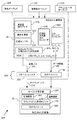
次に図1を参照すると、マイクロプロセッサ10を示すブロック図が図示されている。マイクロプロセッサ10は、FMA計算を実行するように構成された複数の実行ユニット45、50、60を有する。マイクロプロセッサ10は、命令キャッシュ15と、命令トランスレータ及び/又はマイクロコードROM20と、リネーム・ユニット及び予約ステーション25と、修正された乗算器45、修正された加算器50、及び他の実行ユニット60を含む複数の実行ユニットと、丸めキャッシュ55(代替的に計算制御インジケータ記憶装置とも称される)と、アーキテクチャ・レジスタ35と、リオーダ・バッファ30(リネーム・レジスタを含む)とを備える。他の機能ユニット(図示せず)は、とりわけ、マイクロコード・ユニットと、分岐予測器と、キャッシュ・メモリ階層(たとえば、レベル1データ・キャッシュ、レベル2キャッシュ)、メモリ順序バッファ、及びメモリ管理ユニットを含むメモリ・サブシステムと、データ・プリフェッチ・ユニットと、バス・インターフェース・ユニットとを備えることができる。マイクロプロセッサ10は、命令がプログラム順序から外れた実行のために発行され得るという点でアウト・オブ・オーダー実行のマイクロアーキテクチャを有する。より具体的には、アーキテクチャ命令(又はマクロ命令)が翻訳又は変換されるマイクロ命令は、プログラム順序から外れた実行のために発行され得る。マイクロ命令のプログラム順序は、それらの翻訳又は変換元のそれぞれのアーキテクチャ命令のプログラム順序と同じである。マイクロプロセッサ10は、クロック・サイクルごとに複数の命令を実行のために実行ユニットに発行することができるという点で、スーパースカラー・マイクロアーキテクチャをさらに有する。一実装において、マイクロプロセッサ10は、x86命令セット・アーキテクチャと互換性のある方式で命令の実行を提供する。
Referring now to FIG. 1, a block diagram illustrating a
命令キャッシュ15は、システム・メモリからフェッチされたアーキテクチャ命令をキャッシュする。命令トランスレータ及び/又はマイクロコードROM20は、命令キャッシュ15からフェッチされたアーキテクチャ命令をマイクロプロセッサ10のマイクロアーキテクチャのマイクロ命令セットのマイクロ命令に翻訳し又は変換する。実行ユニット45、50、60が、マイクロ命令を実行する。アーキテクチャ命令の翻訳又は変換先のマイクロ命令が、アーキテクチャ命令を実装する。リネーム・ユニット25は、プログラム順序におけるマイクロ命令のためにROB30内にエントリを受け取り、割り振り、割り振られたROBエントリのインデックスでマイクロ命令を更新し、各マイクロ命令をマイクロ命令を実行する実行ユニットに関連付けられている適切な予約ステーション25にディスパッチし、マイクロ命令に対するレジスタ・リネーミング及び依存関係生成を実行する。
型による計算の分類 Classification of calculations by type
本発明の一実装の一態様において、FMA計算は、変数ExpDeltaによって示される、入力オペランドの指数値の差、及びFMA計算が実効減算(effective subtraction)を伴うかどうかに基づき区別される。図2は、値ExpDeltaを表す数直線70を含む数空間65を示している。数直線70より下の領域は、計算が実効減算を構成することを表す。数直線70より上の領域は、計算が実効加算を構成する(すなわち、実効減算はない)ことを表す。
In one aspect of one implementation of the present invention, FMA calculations are distinguished based on the difference in the exponent values of the input operands indicated by the variable ExpDelta and whether the FMA calculation involves effective subtraction. FIG. 2 shows a
指数差ExpDeltaは、乗数及び被乗数入力指数値の和から任意の指数バイアス値を引き、加数又は減数入力指数値を引いた値である。アキュムレータがバイアス調整された積ベクトルよりもかなり大きい計算は、負のExpDeltaで特徴付けられる。同様に、アキュムレータがバイアス調整された積ベクトルよりもかなり小さい計算は、正のExpDeltaで特徴付けられる。 The exponent difference ExpDelta is a value obtained by subtracting an arbitrary exponent bias value from the sum of a multiplier and a multiplicand input exponent value and subtracting an addend or subtract input exponent value. Calculations where the accumulator is much larger than the biased product vector are characterized by a negative ExpDelta. Similarly, calculations where the accumulator is much smaller than the biased product vector are characterized by a positive ExpDelta.
変数EffSubによって示される「実効減算」は、入力オペランドの符号及び所望される演算(たとえば、乗算加算又は乗算減算)が組み合わさって、結果の大きさの実効増加ではなく浮動小数点数結果の大きさの実効減少を引き起こすことを示す。たとえば、負の被乗数が正の乗数で乗算され(負の積)、次いで正の被加数に加算されたときに、結果の大きさの実効減少をもたらし、実効減算(EffSub)と指定される。 The “effective subtraction” indicated by the variable EffSub is a combination of the sign of the input operand and the desired operation (eg, multiplication addition or multiplication subtraction), resulting in a floating-point result magnitude rather than an effective increase in result magnitude. It shows that it causes an effective decrease of. For example, when a negative multiplicand is multiplied by a positive multiplier (negative product) and then added to the positive algebra, it results in an effective reduction of the magnitude of the result, designated as effective subtraction (EffSub) .
図2の数空間65の右側に示されているように、積ベクトルの大きさが結果を支配している場合、アキュムレータは、初めのラウンド・ビット又はスティッキー・ビット計算に直接寄与することができる。以下で説明されているように、アキュムレータと積の仮数との相対的アライメントは、丸めに寄与するビットを計算する前に2つを足し合わせることを奨励する。図2の数空間65は、「実効減算」がないそのようなケースを「2型」計算80として、実効減算があるそのようなケースを「4型」計算90として指定する。
If the magnitude of the product vector dominates the result, as shown on the right side of
図2の数空間65の左側に示されているように、アキュムレータの大きさが結果を支配し、アキュムレータの仮数のサイズが所望の結果の仮数のサイズよりも小さいか、又は等しいときに、アキュムレータは初めのラウンド・ビット又はスティッキー・ビット計算に寄与し得ない。図2の数空間65は、「実効減算」がないそのようなケースを「3型」計算85として、実効減算があるそのようなケースを「5型」計算95として指定する。アキュムレータは、積の仮数の左に効果的にアライメントされるので、アキュムレータを加算する前にいくつかのスティッキー・ビット及びラウンド・ビットを識別することによって利点が実現され得る。
As shown on the left side of
ExpDeltaが図2の数直線70の右側にある状況を、ExpDeltaが図2の数直線70の左側にある状況から区別することには多くの利点がある。たとえば、従来のFMAは、極端に広い、入力仮数幅の3倍程度又はそれ以上のアライメント・シフターを利用して、アキュムレータが被乗数と乗数との積の左又は右にアライメントされ得る計算を考慮する。FMA計算を2つの修正された実行ユニット(修正された乗算器45と修正された加算器50)によって実行される2つのサブ演算に分割することによって、より小さいデータ経路及びより小さいアライメント・シフターを利用することが可能である。
There are many advantages to distinguishing the situation where ExpDelta is on the right side of the
数直線70の右側の計算では、アキュムレータは、中間積ベクトルよりも小さい大きさを有する。ここで、修正された乗算器45内で乗算器積にアキュムレータを加算することは有利である。そのような計算に対して、従来のFMAのデータ経路幅より小さい、ほぼ1つの仮数の幅であるデータ経路幅で十分である。修正された乗算器45は、すでに、何らかの固有の遅延を有しているので、アキュムレータは、総和ツリー/アレイと効率的にアライメントされる。正規化及び丸めも簡素化される。丸めは、修正された加算器50によって第2のFMAサブ演算において実行される。
In the calculation to the right of the
数直線70の左側の計算では、対照的に、アキュムレータは、より大きいオペランドとなり、丸めに寄与し得ない。アキュムレータが丸めに寄与していないので(次に説明される特別なケースを除いて)、乗数積に対して何らかの初めのスティッキー・コレクション(sticky collection)を実行すること、中間結果をメモリ(たとえば、リオーダ・バッファ及び/又はキャッシュ)に保存すること、及び修正された加算器50を使用してアキュムレータを総和することが可能である。従来の丸めロジックでは、アキュムレータが丸め判断に寄与しない特別なケースを効果的に取り扱い、和のオーバーフローがある場合、ラウンド・ビットはスティッキー・ビットのうちの1つになり、和のLSBがラウンド・ビットになる。
In the calculation on the left side of the
いくつかの種類のFMA計算−図2の数空間65の下半分に示されている「実効減算」計算のサブセット−の結果、最上位桁の1つ又は複数がゼロに設定され得る。当業者は、これを「マス・キャンセル」と称する。図2において、マス・キャンセルに対する潜在的可能性が存在する計算は、「1型」計算75として指定される。そのような場合、丸め点がどこにあるかを決定するために、丸めに先だって正規化が必要になる場合がある。ベクトルを正規化する際に関わるシフト演算は、著しい時間遅延を引き起こし、且つ/或いは先頭桁予測の使用を必要とする場合がある。その一方で、先頭桁予測は、マス・キャンセルを伴わないFMA計算に対してはバイパスされ得る。
As a result of some types of FMA calculations—a subset of the “effective subtraction” calculations shown in the lower half of
要するに、FMA計算は、図2に示されているように、ExpDelta及びEffSubに基づきいくつかの型にソートされる。第1のFMA計算型75は、EffSubが真である範囲{−2,−1,0,+1}内のExpDeltaでの計算を含むように定義される。これらは、ビットのマス・キャンセルに対する潜在的可能性が対処される計算を含む。第2のFMA計算型80は、EffSubが偽の場合にExpDeltaが−1以上での計算を含む。第3のFMA計算型85は、EffSubが偽の場合にExpDeltaが−2以下での計算を含む。第4のFMA計算型90は、EffSubが真でありExpDelta値が{+1}よりも大きい計算を含む。第5のFMA計算型95は、EffSubが真でありExpDelta値が{−2}よりも小さい計算を含む。本明細書で説明されている型の指定は、単なる例であること、及び型は異なる仕方で定義され得ることも理解されるであろう。たとえば、一実装において、2型及び4型が、単一のユニタリ型(unitary type)として記述されてもよく、同様に、3型及び5型が、単一のユニタリ型として記述されてもよい。さらに、図2の数直線70の右部分と左部分との間の分割線(破線で示されている)は、実装が異なれば異なり得る。
In short, FMA calculations are sorted into several types based on ExpDelta and EffSub, as shown in FIG. The first
融合FMA命令実行コンポーネント・セット Integrated FMA instruction execution component set
図3は、FMA計算を実行するように構成された融合FMA命令実行コンポーネント・セット100の一実施形態の一般化された図を示している。コンポーネント・セット100は、2つの物理的に及び/又は論理的に別個の算術演算ロジック・ユニット−一実装では修正された乗算器45及び修正された加算器50−と複数の丸められていない中間結果ベクトル及び丸めインジケータを記憶するための共有記憶装置155及び55とを備える。
FIG. 3 shows a generalized diagram of one embodiment of a fused FMA instruction execution component set 100 configured to perform FMA calculations. The component set 100 comprises two physically and / or logically separate arithmetic logic units—a modified
修正された乗算器45及び修正された加算器50の各々は、命令実行ユニットであり、より具体的には、マシン・レベルの命令(たとえば、CISCマイクロアーキテクチャの命令の指定されたセット又はRISCマイクロアーキテクチャのマイクロ命令の指定されたセット)をデコードし、そのオペランドを共有高速メモリのコレクションから読み出し、その結果を該メモリのコレクションに書き込む命令パイプライン24内の算術処理ユニットである。命令実行ユニットは、完了のためそれに対して意図的に配送されたマシン・レベルの命令の指定されたセットを実行するように用意されたロジック回路の特性セットとして理解されてもよく、並列(及び単にパイプライン化されているだけでない)様式で複数のマシン命令を実行するように動作可能な回路のより大きなクラスタ(もし存在すれば)と対照的である。
Each of the modified
より具体的には、修正された乗算器45及び修正された加算器50は、マイクロ命令をデコードし、マイクロ命令に基づき独立して演算し、制御信号を内部データ経路に提供することができる、別個のアトミックなスタンドアロン実行ユニットである。共有高速メモリは、データを交換し、その結果を他の実行ユニットに見せるようにマイクロ命令に提供される、非アーキテクチャ計算用レジスタのセット又はレジスタ・ファイルであってよい。
More specifically, the modified
より具体的には、修正された乗算器45は、ほとんどの態様において、FMA演算の一部ではない通常の乗算マイクロ命令を実行することができるという点で従来型であり得る好適な乗算計算ユニットである。しかし、これは、以下でさらに説明されているように、FMA乗数105、被乗数110、及びアキュムレータ115を入力オペランドとして受け取り、記憶形式中間結果150を作り出すために、適切な修正を有する。同様に、修正された加算器50は、ほとんどの態様において、加算又は減算などの、FMA演算ではない通常の累算マイクロ命令を実行することができるという点で従来型であり得る好適な加算器計算ユニットである。しかし、これは、記憶形式中間結果150を受け取り、正しい丸められたFMA結果を作り出すために、適切な修正を有する。
More specifically, the modified
修正された乗算器45は、融合FMA演算の第1のステージ又は部分(FMA1サブ演算)を実行することができる。修正された乗算器45は、入力オペランド・アナライザー140と、乗算器総和アレイ120と、最終加算器125と、正規化シフター130と、先頭桁予測器及びエンコーダ135とを備える。FMA1サブ演算を実行するときに、修正された乗算器45は、丸められていない正規化された総和結果145と複数の丸めビット(又は丸めインジケータ)とを生成し、出力する。その一方で、非融合FMA演算を実行するときに、修正された乗算器45は、丸められたIEEE準拠結果を生成する。
The modified
丸めビットと丸められていない正規化された総和結果145の最上位ビット(most significant bits;MSB)とは、記憶形式に従って記憶される。一実装において、丸められていない正規化された総和結果145のMSBは、ターゲット・データ形式の仮数幅に等しい仮数幅を有するリネーム・レジスタ155に記憶するために、結果バス146上に出力される。丸めビットは、リネーム・レジスタ155を記憶する記憶装置ユニット(たとえば、リオーダ・バッファ30)から区別できる丸めキャッシュ55内に記憶するために、修正された乗算器の外部にあり結果バス146から区別できる専用の丸めビット若しくは計算制御インジケータ・データ経路又は接続ネットワーク148上に出力される。丸められていない正規化された総和結果145のMSBは、丸めビットとともに、記憶形式中間結果150を一緒に構成する。
The rounded bits and the most significant bits (MSB) of the normalized summation result 145 not rounded are stored according to the storage format. In one implementation, the MSB of the unrounded normalized sum result 145 is output on the
リネーム・レジスタ155及び丸めキャッシュ55は、他の実行ユニットから見える共有メモリの一部であるので、修正された乗算器45から物理的に及び/又は論理的に別個である、修正された加算器50は、オペランド・バス152及び丸めビット・データ経路148を介して記憶形式中間結果150を受け取り、融合FMA演算の第2の(完了)ステージ又は部分(FMA2サブ演算)を実行することができる。さらに、FMA1とFMA2との間に、他の無関係の演算が実行され得る。
A modified adder that is physically and / or logically separate from the modified
修正された加算器50は、修正された乗算器45がすでに必要な累算を実行していたFMAの状況においてアキュムレータ・オペランドをゼロに設定するために、オペランド修正器160を備える。修正された加算器50は、最終的な丸められた結果を作り出すために丸めモジュール180においてどの丸めビット−修正された乗算器45によって生成される丸めビット、又は修正された加算器50の内部生成丸めビット、又は両方の何らかの組合せ−を使用するかを選択するためのラウンド・ビット選択ロジック175をさらに備える。修正された加算器50は、2つの累算オペランドのマス・キャンセルの場合に総和を正規化するための近接経路総和回路165と、1ビット分のシフトしか必要としない総和を作り出す累算を実行するための遠隔経路総和回路170とをさらに備える。以下でさらに説明されているように、FMA2サブ演算は、全体として遠隔経路総和回路170によって処理され得る。
The modified
修正された乗算器 Modified multiplier
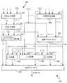
図4及び5は、修正された乗算器45の一実施形態のより詳細な図を示している。図4は、具体的に、修正された乗算器45の経路決定ロジック185及び仮数乗算器モジュール190を示している。図5は、具体的に、修正された乗算器45の指数結果生成器260及び丸めインジケータ生成器245を示している。
4 and 5 show a more detailed view of one embodiment of the modified
図4に示されているように、経路決定ロジック185は、入力デコーダ200と、入力オペランド・アナライザー140と、経路制御ロジック215と、アキュムレータ・アライメント及び注入ロジック回路220とを備える。仮数乗算器モジュール190は、図3の乗算器総和アレイ120を含み、これは図4において2つのコンポーネント、乗算器アレイ235及び部分積加算器240として表されている。仮数乗算器モジュール190は、最終加算器125と、先頭桁予測器及びエンコーダ135と、正規化シフター130とをさらに備える。
As shown in FIG. 4, the
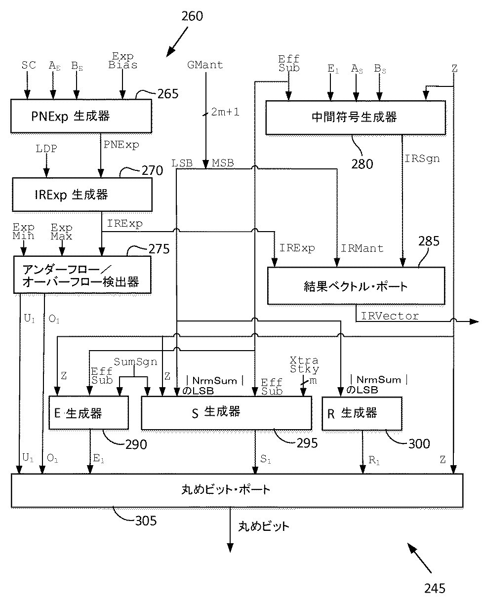
図5に示されているように、指数結果生成器260は、PNExp生成器265、IRExp生成器270、及びアンダーフロー/オーバーフロー検出器275を備える。丸めインジケータ生成器245は、中間符号生成器280、結果ベクトル・ポート285、循環桁上げインジケータ290、スティッキー・ビット生成器295、及びラウンド・ビット生成器300を備える。
As shown in FIG. 5, the
図4に再び注意を向けると、修正された乗算器45は、1つ又は複数の入力ポート195を通じて入力マイクロ命令及びオペランド値を受け取る。FMAマイクロ命令の場合、修正された乗算器45は、被乗数オペランドA、乗数オペランドB、及びアキュムレータ・オペランドCを受け取り、これらの各々が、符号インジケータ又はビットと、仮数と、指数とを含む。図4及び6において、浮動小数点オペランドの符号、仮数、及び指数コンポーネントは、それぞれ、添字S、M、及びEによって表される。したがって、たとえば、AS、AM、及びAEは、それぞれ、被乗数符号ビット、被乗数仮数、及び被乗数指数を表す。
Turning again to FIG. 4, the modified
デコーダ200は、FMAインジケータMと2進数演算符号インジケータ(又はビット)PS及びOSとを生成するために入力マイクロ命令をデコードする。Mは、FMAマイクロ命令を受け取ることを表す。一実装において、A*B+Cの形式のFMAマイクロ命令は、結果として、2進数ゼロの正乗算/ベクトル負乗算符号演算子PSと2進数ゼロの加算/減算演算子OSとの生成を引き起こす。−A*B+Cの形式の負乗算加算マイクロ命令は、結果として、2進数1のPSと2進数0のOSとを生じる。A*B−Cの形式の乗算減算マイクロ命令は、結果として、2進数0のPSと2進数1のOSとを生じ、−A*B−Cの形式のベクトル負乗算減算マイクロ命令は、結果として、2進数1のPS及びOSを生じる。他のより単純な実装では、修正された乗算器45は、ベクトル負マイクロ命令及び/又は減算マイクロ命令を直接サポートしないが、マイクロプロセッサ10は、乗算加算/減算マイクロ命令を修正された乗算器45にディスパッチする前に最初に1つ又は複数のオペランド、又は符号インジケータを適宜加法的に反転することによって同等の演算をサポートする。
The
乗算器アレイ235は、被乗数及び乗数の仮数値AM及びBMを受け取り、AMとBMとの部分積を算出する。(AM及びBMのいずれかの絶対値が1又は0である場合、乗算器アレイ235は、AMとBMとの完全な積を構成するであろう単一の「部分積」値を作り出し得ることが理解されるであろう。)部分積は、部分積加算器240に供給され、部分積加算器240は、AとBとのこうした部分積をこれらを総和する準備において受け取るための複数のエントリを備える。部分積加算器240内のエントリのうちの少なくとも1つは、アキュムレータ導出値CXを受け取るように構成される。部分積加算器240の追加の説明は、入力オペランド・アナライザー140とアキュムレータ・アライメント及び注入ロジック220との説明の後、以下で再開する。
The
入力オペランド・アナライザー140は、ExpDeltaアナライザー・サブ回路210及びEffSubアナライザー・サブ回路205を備える。ExpDeltaアナライザー・サブ回路210は、ExpDelta(ExpΔ)値を生成する。一実装において、ExpDeltaは、乗数及び被乗数入力指数値AE及びBEを総和し、加数又は減数入力指数値CEを減算し、もしあれば、指数バイアス値ExpBiasを減算することによって計算される。ExpBias値を導入することで、AE、BE、及びCEが、たとえばIEEE754によって要求されるような、バイアスされた指数を使用して表されるときに、被乗数Aと乗数Bとの積が、アキュムレータCのバイアスの2倍のバイアスを有するという事実を補正する。
The
EffSubアナライザー・サブ回路205は、オペランド符号インジケータAS、BS、及びCSと、演算子符号インジケータPS及びOSとを分析する。EffSubアナライザー・サブ回路205は、FMA演算が実効減算となるかどうかを指示する「EffSub」値を生成する。たとえば、実効減算は、AとBとの積(又は負ベクトル乗算演算子についての負の積)に対するCの演算子指定の加算又は減算が(a)AとBとの積の絶対値の大きさ、又は(b)Cの絶対値の大きさ、よりも小さい絶対値の大きさを有する結果Rをもたらす場合に、結果として生じる。数学的記法で表された場合、FMA演算は、(|R|<|A*B|)∨(|R|<|C|)の場合に実効減算を構成し、ここで、RはFMA演算の結果である。EffSubをFMA演算の結果に関して記述すると都合がよいが、EffSubアナライザー・サブ回路205は、A、B、及びCの仮数、指数、又は大きさを評価することなく、符号インジケータAS、BS、CS、PS、及びOSを分析することによってEffSubを事前に決定することが理解されるであろう。
The
経路制御ロジック215は、入力オペランド・アナライザー140によって生成されるExpDelta及びEffSubインジケータを受け取り、それに応答して、経路制御信号を生成し、その値は、ここでは変数Zによって参照される。経路制御信号Zは、Cの累算がAとBとの部分積とともに修正された乗算器45内で実行されるかどうかを制御する。一実装において、Zを生成するために経路制御ロジック215が使用する基準は、図2に規定されている。一実装において、Zは、修正された乗算器45が乗算加算演算の累算部分を実行するように選択されるすべてのケース(たとえば、1、2、及び4型)に対して2進数の1であり、ExpDelta及びEffSubの他のすべての組合せ(たとえば、3及び5型)に対して2進数の0である。
The
代替的に、経路制御ロジック215がZを生成するために使用し得る基準は、Cが、AとBとの積の大きさに対して、AとBとの部分積総和のための総和ツリー内に提供される最上位ビットの左にCの最上位ビットをシフトすることなく、総和ツリー内でCのアライメントを行うことが可能な大きさを有するかどうかである。別の、又は代替的な基準は、FMA演算を実行する際のマス・キャンセルに対する潜在的可能性があるかどうかである。さらに別の、又は代替的な基準は、AとBとの積に対するCの累算が、AとBとの積とCとをアライメントするのに必要なビットよりも少ないビットを必要とする丸められていない結果Rを生成するかどうかである。こうして、経路制御基準は修正された乗算器45の設計に依存して変わり得ることが理解されるであろう。
Alternatively, the criteria that the
アキュムレータ・アライメント及び注入ロジック220回路は、経路制御ロジック215によって生成されたZと、ExpDeltaアナライザー・サブ回路210によって生成されたExpDeltaと、シフト定数SCと、アキュムレータ仮数値CMとを受け取る。一実装において、アキュムレータ・アライメント及び注入ロジック220は、CMのビット単位の否定
Accumulator alignment and
[外1]
これらの入力に応答して、アキュムレータ・アライメント及び注入ロジック220回路は、部分積加算器240内に注入する値CXを作り出す。CXを保持するアレイの幅は、2m+1、又は入力オペランド仮数AM、BM、及びCMの幅の2倍プラス1追加ビットである。
In response to these inputs, the accumulator alignment and
Mが2進数の0であり、修正された乗算器45がFMA1サブ演算ではなく通常の乗算演算を実行していることを示している場合、マルチプレクサ230が、CXの代わりに丸め定数RCを部分積加算器240内に注入して、修正された乗算器45が従来の様式で丸められた結果を生成できるようにする。RCの値は、命令によって指示された丸めの型(たとえば、切り上げへの0.5の丸め(round half up)、偶数への0.5の丸め(round half to even)、0から遠い方への0.5の丸め(round half away from zero))と、さらに入力オペランドのビット・サイズ(たとえば、32ビット対64ビット)とに、部分的に依存する。一実装において、部分積加算器240は、2つの異なる丸め定数を使用して、2つの和を算出し、次いで、適切な和を選択する。修正された乗算器45のIMant出力は、これによって、通常の乗算演算の正しく丸められた仮数結果となる。
If M is binary 0, indicating that the modified
Mが2進数の1で、Zが2進数の0であり、Cの累算が部分積加算器240によって実行されるべきでないことを指示している場合、一実装において、アキュムレータ・アライメント及び注入ロジック220回路は、CX=0を設定し、マルチプレクサ230に、CXを受け取るために提供される部分積加算器240内に0を注入することを行わせる。Mが2進数の1で、Zが2進数の1である場合、アキュムレータ・アライメント及び注入ロジック220は、ExpDelta+シフト定数SCに等しい量だけCMを右シフトし、CXを作り出す。一実装において、シフト定数SCは2に等しく、これは、Cとの累算が修正された乗算器45内で実行される図2の数空間内の最大の負のExpDeltaに対応する。次いで、マルチプレクサ230は、その結果得られるCXを部分積加算器240に注入する。
In one implementation, accumulator alignment and injection, where M is binary 1 and Z is binary 0, indicating that accumulation of C should not be performed by
アキュムレータ・アライメント及び注入ロジック220は、さらに、スティッキー・コレクタを組み込む。部分積加算器240の総和ツリーの最下位ビット(least significant bit;LSB)を超えてシフトされるアキュムレータCXの任意の部分が、XtraStkyビットとして保持され、丸めに使用される。m個までのビットは、部分積加算器240のLSBを超えてシフトされ得るので、XtraStkyビットは、m幅の追加スティッキー・ビット・アレイとして転送され、スティッキー・ビットSを計算する際に使用される。
The accumulator alignment and
修正された乗算器45の総和ロジックに再び注意すると、部分積加算器240は、いくつかの実装において総和ツリーであり、一実装において1つ又は複数の桁上げ保存加算器である。部分積加算器240は、部分積の総和の中にこの追加の選択的にビット単位否定されアライメントされたアキュムレータ入力値を含み、従来技術の乗算実行ユニットに典型的な方法に従い、提供された部分積総和ツリー内のビットの列上の桁上げ保存ベクトルごとに、丸められていない冗長表現又は和への総和を実行する。
Returning again to the summation logic of the modified
ここでもまた、部分積加算器240によって実行される数学演算は、Zの値に依存することが理解されるであろう。Z=1の場合、部分積加算器240は、AMとBMとの部分積とCXの連帯累算(joint accumulation)を実行する。Z=0の場合、部分積加算器240は、AMとBMとの部分積の一次累算を実行する。一次又は連帯累算の結果として、部分積加算器240は、2mビット和ベクトル及び2mビット桁上げベクトルとして表される冗長2進数和を作り出す。
Again, it will be understood that the mathematical operations performed by the
桁上げ及び和ベクトルは、最終加算器125と先頭桁予測器及びエンコーダ135との両方に転送される。最終加算器125は、桁上げ先見加算器又は桁上げ伝播加算器であってよく、桁上げ及び和ベクトルを2m+1の幅を有する正又は負の事前正規化された丸められていない非冗長和PNMantにコンバートすることによって総和プロセスを完了する。最終加算器125は、PNMantが正か又は負かを指示する和符号ビットSumSgnをさらに生成する。
The carry and sum vectors are transferred to both the
最終加算器125がPNMantを生成するのと並行して、また同じ時間間隔の間に、先頭桁予測器及びエンコーダ135は、PNMantを正規化するためにキャンセルされる必要のある先頭桁の数を予想する。この配置構成は、最終加算器125による最終加算が正規化の後に行われる従来技術の分割された乗算加算FMA設計に勝る利点をもたらす。これは、桁上げベクトルと和ベクトルの両方の正規化を必要とするものであり、今度は、先頭桁予測の出力を待たなければならない。好ましい一実装において、先頭桁予測器及びエンコーダ135は、正又は負のいずれかの和を収容する。
In parallel with the
一実装において、先頭桁予測は、1型計算に対してのみ実行される。先頭桁予測の選ばれた方法は、すでに説明されているように、また浮動小数点計算設計の実務における当業者に理解されるように、正又は負のいずれかの和を収容する。
In one implementation, leading digit prediction is performed only for
先頭桁予測器及びエンコーダ135は、最大1ビットの不正確さを有し得るので、これを補正するためのいくつかの通常使用される技術が正規化シフター130において、又はそれに関して提供され得る。一アプローチは、この不正確さを予想するロジックを提供することである。別のアプローチは、PNMantのMSBがセットされているかいないかを調べ、それに応答して、PNMantの追加のシフトを選択することである。
Since the leading digit predictor and
正規化シフター130は、最終加算器125から丸められていない非冗長和PNMantを受け取り、初期仮数値GMantを生成する。CXとの累算が部分積加算器240を使用して実行されている場合、GMantは、CXと、AMとBMとの積との、絶対的な正規化された和である。他のすべての場合において、GMantは、AMとBMとの積の、絶対的な正規化された和である。
The
GMantを作り出すために、正規化シフター130は、PNMantが負であることをSumSgnが指示する場合、PNMantをビット単位で否定する。負のPNMant値についての正規化シフター130のビット単位の否定は、以下でさらに説明されているように、記憶形式中間結果150の生成において有用である。さらに、正しい丸めを容易にすることにおいても有用である。修正された乗算器においてPNMantを反転することによって、PNMantは、それが負数であったことを伝えることなく、修正された加算器に正数として提供され得る。これは、累算が和として実装され、簡素化された方式で丸められることを可能にする。
To create GMant,
さらに、正規化シフター130は、PNMantをLDP、EffSub、及びZの関数である量だけ左シフトする。最上位先頭桁のキャンセルが生じない場合であっても、有用な標準化された記憶形式中間結果150を作り出し、正しいその後の丸めを可能にするために、0、1、又は2ビット位置によるPNMantの左シフトが必要とされ得ることに留意されたい。左シフトからなる正規化は、算術的最上位桁を標準化された最も左の位置に移動し、それを以下でさらに説明されている記憶形式中間結果150で表現することができる。
Further, the
この実装は、従来技術のFMA設計に勝る3つの追加の利点を実現する。第1に、EffSubに応答してアキュムレータ仮数上で2の補数が実行される場合に必要とされるであろうようには、追加の桁上げビットを部分積加算器240に挿入する必要がない。第2に、大きい符号ビット検出器/予測器モジュールを提供し非冗長部分積及びアキュムレータ総和値の冗長和及び桁上げベクトル表現を調べて選択的に補数をとる必要がない。第3に、追加の桁上げビット入力を提供し部分積及びアキュムレータ総和の上記ような選択的に補数をとられた和及び桁上げベクトル表現に対する正しい計算を保証する必要がない。
This implementation provides three additional advantages over prior art FMA designs. First, there is no need to insert additional carry bits into the
次に、図5の指数結果生成器260を参照すると、PNExp生成器265は、事前正規化された指数値PNExpを、被乗数及び乗数指数値AE及びBEと指数バイアスExpBiasとシフト定数SCとの関数として生成する。より具体的には、一実装において、PNExpは、シフト定数SCにAE+BE−ExpBiasを加えたものとして計算される。
Referring now to the
IRExp生成器270は、正規化シフター130によって実行される仮数の正規化を考慮するようにPNExpをデクリメントし、PNExp及び先頭桁予測LDPの関数である中間結果指数IRExpを生成する。次いで、IRExpは結果ベクトル・ポート285に転送されるが、これは以下でさらに説明されている。
The
中間符号生成器280は、中間結果符号インジケータIRSgnを、EffSub、E、AS、BS、及びZの関数として生成する。より具体的には、一実装において、IRSgnは、いくつかの場合において、被乗数符号ビットASと乗数符号ビットBSとの排他的論理和(XOR)として計算される。しかし、Zビットが2進数の1であり、累算が実行されていることを示し、EffSubも2進数の1であり、実効減算であることを示し、Eビット値が2進数の0であり、循環桁上げが保留になっていないことを示す場合、IRSgnは、有利には、被乗数符号ビットASと乗数符号ビットBSとの否定排他的論理和(XNOR)として計算される。別の言い方をすれば、中間符号は、一般的に、AとBとの積の符号である。AとBとの積の符号は、アキュムレータがAとBとの積よりも大きい大きさを有するときに逆にされ、乗算加算演算は実効減算であり、累算の完了は循環桁上げを必要としない(累算が負であるため)。
中間結果符号インジケータIRSgnは、マス・キャンセルが起こり得ることであるFMA計算についての最終符号ビットを決定するための革新的方法に寄与する。従来技術の分割経路FMA実装とは異なり、本明細書で説明されている実装は、符号予測を必要とせず、また符号予測する際に採用されるかなり大きい回路を必要としない。代替的に、ゼロの結果の符号、又は符号付きゼロ入力による計算からの結果の符号は、容易に事前算出されることができ、たとえば、丸めモード入力を組み込む。 The intermediate result sign indicator IRSgn contributes to an innovative method for determining the final sign bit for the FMA calculation where mass cancellation can occur. Unlike the prior art split path FMA implementation, the implementation described herein does not require code prediction and does not require the much larger circuitry employed in code prediction. Alternatively, the sign of the result of zero, or the sign of the result from a calculation with a signed zero input, can easily be precomputed, for example incorporating a rounding mode input.
結果ベクトル・ポート285は、中間結果指数IRExpと中間結果符号IRSgnと中間結果仮数IRMantとを含む記憶形式中間結果ベクトルIRVectorを出力する。記憶形式の一実装において、IRMantは、GMantの最上位mビットを含み、ここで、mは、ターゲット・データ型の幅である。たとえば、IEEE double double精度計算において、結果ベクトル・ポート285は、IRVectorを、単一の符号ビットと11個の指数ビットとGMantの最上位53ビットとの組合せとして出力する。記憶形式の別の実装において、mは、仮数値AM、BM、及びCMの幅に等しい。さらに別の実装において、mは、仮数値AM、BM、及びCMの幅よりも大きい。
The
これらの仮数ビットの単一の最上位ビットは、記憶されるときに暗黙の値を仮定することができ、これはIEEE標準記憶形式に類似している。IRVectorは、ROB30のリネーム・レジスタ155などの共有メモリに保存され、したがって、他の命令実行ユニットによってアクセスされ、且つ/或いは結果転送バス40上で別の命令実行ユニットに転送され得る。好ましい一実装において、IRVectorは、リネーム・レジスタ155に保存される。さらに、中間結果ベクトルは、ROB30内で永続的な割り当てを与えられ得るアーキテクチャ・レジスタと異なり、ROB内で予測不可能な割り当てを与えられる。代替的実装において、IRVectorは、FMA演算の最終的な丸められた結果が記憶されるデスティネーション・レジスタに一時的に保存される。
The single most significant bit of these mantissa bits can assume an implicit value when stored, which is similar to the IEEE standard storage format. The IRVector may be stored in a shared memory, such as the
次に、図5の丸めインジケータ生成器245を参照すると、アンダーフロー/オーバーフロー検出器275は、アンダーフロー・インジケータU1及びオーバーフロー・インジケータO1を、記憶形式中間結果150(以下でさらに説明されている)の精度又はターゲット・データ型に対応する、IRExpと指数範囲値ExpMin及びExpMaxとの関数として生成する。IRExpが、このFMA計算のターゲット・データ型に対する表現可能な指数値の範囲よりも小さいか、又はリネーム・レジスタなどの中間記憶装置に対する表現可能な指数値の範囲よりも小さい場合、U1ビットは2進数の1を割り当てられる。そうでない場合、U1ビットは、2進数の0を割り当てられる。逆に、IRExpが、このFMA計算のターゲット・データ型に対する表現可能な指数値の範囲よりも大きいか、又はリネーム・レジスタなどの中間記憶装置に対する表現可能な指数値の範囲よりも大きい場合、O1ビットは2進数の1を割り当てられる。そうでない場合、O1ビットは、2進数の0を割り当てられる。代替的に、U&Oは、4つのとり得る指数範囲を表すようにエンコードされてもよく、そのエンコーディングのうちの少なくとも1つはアンダーフローを表し、そのうちの少なくとも1つはオーバーフローを表す。
Referring now to the rounding
U1及びO1ビットは、通常の乗算器ユニットの従来の実装では、例外制御ロジックに報告される。しかし、FMA1サブ演算を実行したときに、修正された乗算器45は、U1及びO1ビットを中間記憶装置に出力し、これは、修正された加算器50によって処理される。
The U 1 and O 1 bits are reported to the exception control logic in conventional implementations of normal multiplier units. However, when performing the FMA1 sub-operation, the modified
循環桁上げインジケータ生成器290は、保留中の循環桁上げインジケータE1ビットを、ZとEffSubとSumSgnとの関数として生成する。E1ビットは、事前に決定されているZビットが2進数値の1を有し、部分積加算器240がCとの累算を実行していたことを指示し、事前に決定されているEffSub変数が結果として実効減算を引き起こした累算を指示し、SumSgnによって指示されているように正の丸められていない非冗長値PNMantが作り出された場合に、2進数の1を割り当てられる。他のすべてのケースにおいて、E1は2進数の0を割り当てられる。
The cyclic
結果ベクトル・ポート285は、GMantの最上位ビットを中間結果ベクトルの中間結果仮数として記憶するが、スティッキー・ビット生成器295及びラウンド・ビット生成器300は、重要度の低い(たとえば、中間結果仮数の53番目のビットを超える)残りのビットをラウンド(R1)及びスティッキー(S1)ビットに低減する。スティッキー・ビット生成器295は、スティッキー・ビットS1を、SumSgnとZとGMantの最下位ビットとEffSubとXtraStkyビットとの関数として生成する。ラウンド・ビット生成器300は、ラウンド・ビットR1をGMantの最下位ビットの関数として生成する。
丸めキャッシュ Rounding cache
丸めビット・ポート305は、ビットU1、O1、E1、S1、R1、及びZの各々を、それらがFMA演算の最終的な丸められた結果を生成するために別の命令実行ユニット(たとえば、修正された加算器50)によってその後使用され得るように出力する。便宜上、これらのビットはすべて、これらのビットのうちのいくつかがFMA演算の最終出力を作り出す際に他の目的に使用され得るとしても、またこれらのビットのすべてが丸めに使用されるとは限らない場合であっても、本明細書では丸めビットと称される。たとえば、いくつかの実装において、O1ビットは、丸めに使用されない場合がある。これらのビットは、計算制御インジケータと交換可能に称され得る。ビットZ及びEは、たとえば、どのようなさらなる計算が実行される必要があるかを指示する。U及びOは、たとえば、それらの計算がどのように進行すべきかを指示する。さらに、これらのビットは、修正された乗算器45のFMA1サブ演算と修正された加算器50のFMA2サブ演算との間の中断において計算状態情報を表し、適宜記憶するためのコンパクト形式を提供するので、計算中断状態値と称され得る。
The rounding
中間結果ベクトル及びアキュムレータ値Cと一緒に、これらのビットは、丸めビット、計算制御インジケータ、計算状態インジケータ、又は何か別の名で称されるとしても、その後の命令実行ユニットが必要とするあらゆるものを、そのオペランド値に加えて提供して、算術的に正しい最終結果を作り出す。別の言い方をすれば、中間結果ベクトルと丸めビットとの組合せは、FMA演算の結果の算術的に正しい表現を作り出すために必要なあらゆるものを提供し、これは、有効桁において(in significance)ターゲット・データ・サイズに低減された±A*B±Cの無限精度FMA計算から生成された結果から区別不能なものである。 Along with the intermediate result vector and accumulator value C, these bits may be referred to as rounding bits, calculation control indicators, calculation status indicators, or whatever else is required by subsequent instruction execution units. Is provided in addition to its operand values to produce an arithmetically correct final result. In other words, the combination of the intermediate result vector and the rounding bit provides everything necessary to produce an arithmetically correct representation of the result of the FMA operation, which is in significant digits. It is indistinguishable from the results generated from the infinite precision FMA calculation of ± A * B ± C reduced to the target data size.
本発明の好ましい一態様に合わせて、マイクロプロセッサ10は、丸めビットを、計算制御インジケータ・ストアとも代替的に称され得る丸めキャッシュ55内に記憶することと、丸めビットを転送バス40上で別の命令実行ユニットに転送することの両方を実行するように構成される。代替的一実装において、マイクロプロセッサ10は、丸めキャッシュ55を有さず、その代わりに、丸めビットを転送バス40上で別の命令実行ユニットに単に転送する。さらに別の代替的実装において、マイクロプロセッサ10は、丸めビットを丸めキャッシュ55内に記憶するが、丸めビットを一方の命令実行ユニットから別の命令実行ユニットに直接転送するための転送バス40を備えていない。
In accordance with a preferred aspect of the present invention, the
丸めキャッシュ55とそれが記憶する丸めビット又は計算制御インジケータとは両方とも非アーキテクチャであり、このことは、命令セット・アーキテクチャ(ISA)の一部として指定されたプログラマから見える信号ソースであるアーキテクチャ・レジスタ及びアーキテクチャ・インジケータ(浮動小数点ステータス・ワードなど)とは対照的に、それらがエンド・ユーザ・プログラマからは見えないことを意味する。
The rounding
本明細書で説明されている丸めビットの特定のセットは例示的であること、及び代替的実装が丸めビットの代替的セットを生成することが理解されるであろう。たとえば、代替的一実装では、修正された乗算器45は、ガード・ビットG1を生成するガード・ビット生成器をさらに備える。別の実装では、修正された乗算器45は、ゼロの結果の符号をさらに事前計算し、その値を丸めキャッシュに保存する。修正された加算器50のその後の計算がゼロの結果をもたらした場合、修正された加算器50は、保存されているゼロ結果符号インジケータを使用して最終的な符号付きゼロ結果を生成する。
It will be appreciated that the particular set of rounding bits described herein is exemplary and that alternative implementations generate an alternative set of rounding bits. For example, in an alternative one implementation, a modified
本発明の別の好ましい態様に合わせて、丸めキャッシュ55は、修正された乗算器45の外部にあるメモリ記憶装置である。しかしながら、代替的一実装では、丸めキャッシュ55は、修正された乗算器45に組み込まれる。
In accordance with another preferred aspect of the present invention, rounding
より具体的には、丸めキャッシュ55は、一実装において、結果バスから命令実行ユニットに独立して結合される。結果バスは、命令実行ユニットから結果を汎用記憶装置に伝達するが、丸めキャッシュ55は、命令実行ユニットに結果バス55とは独立して結合される。さらに、計算制御インジケータ記憶装置は、計算制御インジケータを記憶又はロードするように動作可能である命令にのみアクセス可能であり得る。したがって、丸めキャッシュ55は、命令結果が出力される結果バスを通じてとは異なるメカニズムによって、たとえば、それ独自のワイヤのセットを通じてアクセスされる。丸めキャッシュ55は、さらに、命令実行ユニットの入力オペランド・ポートを通じてとは異なるメカニズムを通じてアクセスされる。
More specifically, the rounding
一実装において、丸めキャッシュ55はフル・アソシアティブ・コンテンツ・アクセス可能メモリであり、並列にディスパッチされ得るFMA1マイクロ命令の最大数と同じ数の書き込みポートと、並列にディスパッチされ得るFMA2マイクロ命令の最大数と同じ数の読み出しポートと、FMA1マイクロ命令がディスパッチされてから命令スケジューラが対応するFMA2マイクロ命令をディスパッチするまでの間に経過し得る時間の最大期間(単位はクロック・サイクル数)及び命令スケジューラの容量に関係する深さ(エントリの数)とを有する。別の実装では、丸めキャッシュ55はより小さく、マイクロプロセッサ10は、丸めキャッシュ55内の空間がFMA1マイクロ命令の丸めビット結果を記憶するのに利用可能でない場合にFMA1マイクロ命令をリプレイするように構成される。
In one implementation, rounding
キャッシュの各エントリは、キャッシュ・データだけでなくキャッシュ・データに関係するタグ値の記憶を提供する。タグ値は、記憶形式中間結果ベクトルを記憶するリネーム・レジスタ155を識別するために使用されるのと同じタグ値であってよい。マイクロプロセッサ10が、第2のマイクロ命令のオペランドを用意/フェッチしているときに、これは、ROBインデックスを使用してリネーム・レジスタ155から記憶されている中間データを取り出し、そのまったく同じインデックスが、丸めキャッシュ55に提供され、中間結果150の残りの部分(すなわち、計算制御インジケータ)を供給することになる。
Each entry in the cache provides storage for tag values related to the cache data as well as the cache data. The tag value may be the same tag value that is used to identify the
有利には、リネーム・レジスタ155に割り振られている量よりも著しく少ない量の物理的記憶装置エントリが丸めキャッシュ55に割り振られ得る。リネーム・レジスタ155の数は、アウト・オブ・オーダー・マイクロプロセッサ又は設計において実行ユニットを飽和したままにするために必要なレジスタ名の数と実行中の(in flight)マイクロ命令の数との関数である。対照的に、丸めキャッシュ55のエントリの望ましい数は、実行中のFMAマイクロ命令のあり得そうな数の関数にされ得る。したがって、非限定的な一例において、マイクロプロセッサ・コアは、65個のリネーム・レジスタ155と、ただし並列で最大8つの算術計算を果たすように8個だけの丸めキャッシュ55エントリとを提供し得る。
Advantageously, a significantly smaller amount of physical storage entries may be allocated to the rounding
代替的一実装は、中間結果ベクトルを記憶して丸めキャッシュ55データに対する追加ビットを提供するために使用されるリネーム・レジスタ155を拡張する(すなわち、リネーム・レジスタを広くする)。これは、潜在的に空間の次善最適な使用であるが、それでも、本発明の範囲内にある。
An alternative implementation extends the
丸めビットは、中間結果ベクトルIRVectorとともに、記憶形式中間結果150を一緒に含む。この説明されている記憶形式は、標準化されたデータ形式に従って丸められていない正規化された総和結果145の最上位ビット(そのうちの1つは暗黙値を有する)を保存及び/又は転送し、E1、Z、U1、及びO1ビットとともに丸められていない正規化された総和結果145の残りの(低減された、又は低減されていない)ビットを保存及び/又は転送し、従来技術に勝る著しい利点をもたらす。
The rounding bit includes the storage result
修正された加算器 Modified adder
次に、図6を参照すると、修正された加算器50は、オペランド修正器160と、アライメント及び調整ロジック330と、単一ビット・オーバーフロー・シフト・ロジック345と対になる遠隔経路累算モジュール340とを備える。オペランド修正器160は、指数生成器335、符号生成器365、加算器丸めビット生成器350、ラウンド・ビット選択ロジック175、及び丸めモジュール180をさらに備える。
Referring now to FIG. 6, the modified
一実装では、修正された加算器50は、分割経路設計を備え、近接計算と遠隔計算とを別個に算出することを可能にすることが留意されるべきであり、これは、浮動小数点計算設計の実務における当業者に理解されるであろう。近接経路計算機能は、マルチビット正規化シフター(図示せず)と対になる近接経路累算モジュール(図示せず)を備えるが、そのような機能は、図6には示されていない。一実装において、入力指数値の差が集合{−1、0、+1}内にある実効減算を構成するオペランドCとDとの通常の累算は、近接経路165に向けられる。他のすべての加算演算は、遠隔経路170に向けられる。有利には、本発明は、修正された加算器50内のすべてのFMA2サブ演算が遠隔経路170に向けられることを可能にする。
It should be noted that in one implementation, the modified
修正された加算器50は、マイクロ命令と2つの入力オペランドとを受け取るための1つ又は複数の入力ポート310を備える。第1の入力オペランドDは、被減数又は第1の加数である。第2のオペランドCは、減数又は第2の加数である。浮動小数点実装では、各入力オペランドは、入力符号、指数、及び仮数値を含み、それぞれS、E、及びMで表される。デコーダ315はマイクロ命令を解釈して、信号QSを使用して、演算が加算であるか又は減算であるかを指示する。デコーダは、マイクロ命令(又はマイクロ命令によって指定されたオペランド参照)をさらに解釈して、信号Mにより、修正された加算器50がFMA2サブ演算を実行すべきである専用マイクロ演算をマイクロ命令が指令するかどうかを指示する。
The modified
修正された加算器50が、FMA2サブ演算を実行するタスクを課されたときに、修正された加算器50は、対応するFMA1サブ演算を実行した修正された乗算器45によってすでに生成されている中間結果ベクトルIRVectorを受け取る。中間結果ベクトルIRVectorは、幅がmビットしかないので、修正された加算器50は、mビットよりも広い仮数を受け入れ又は処理するように修正される必要がなく、一実装ではそのように修正されない。したがって、修正された加算器50の内部データ経路、累算モジュール340、及び他の回路は、より広い形式で提示されるIRVectorである必要があり又はそうであった場合よりも単純で、効率的である。また、マス・キャンセルに対する潜在的可能性を伴う累算は、修正された乗算器45によって行われるので、FMA結果を正しく計算するために修正された加算器50の近接/マス・キャンセル経路に加えなければならない丸めロジックはない。
When the modified
一実装において、修正された加算器50は、リネーム・レジスタ155からIRVectorを受け取る。別の実装では、IRVectorは、転送バス40から受け取られる。図6に例示されている実装では、IRVectorは、オペランドDとして受け取られ得る。修正された加算器50は、他のオペランドとして、アキュムレータ値Cを受け取る。
In one implementation, the modified
Mが、修正された加算器50がFMA2サブ演算を実行するタスクを課されていることを指示する場合、オペランド修正器160は、Zが2進数の1であり、Cの累算が修正された乗算器45で実行されていることを指示するときに、1つの入力オペランドの一部を2進数の0に等しくなるように設定する。一実装において、指数、仮数、及び符号フィールドCE、CM、及びCSの各々は、0に修正される。別の実装では、指数及び仮数フィールドCE及びCMのみが2進数の0に修正され、オペランド符号CSは保持される。その結果、修正された加算器50は、加数Dと2進数符号付き0とを総和する。
If M indicates that the modified
2進数の1のMのビットは、さらに、修正された加算器50に、修正された乗算器45によって生成され、記憶形式中間結果150に組み込まれた丸めビットを受け取るように、信号で伝える。
The binary 1 M bits are further signaled to the modified
他のすべてのケース、すなわち、Zが2進数の0である場合、又はMが2進数の0である場合で、修正された加算器50が従来の累算演算のタスクを課されていることを指示するとき、オペランド修正器160は、従来の浮動小数点加算に必要な可能性があるもの以外の指数及び仮数フィールドCE及びCMを修正しない。
In all other cases, i.e. when Z is binary 0 or when M is binary 0, the modified
一実装において、オペランド修正器160は、Zの値を受け取ってCMと0との間、及びCEと0との間で選択する一対のマルチプレクサを備える。選択された値は、図6上でCM*及びCE*として表される。次いで、アライメント及び調整ロジック330は、選択された値CM*及び第1のオペランド仮数DMのアライメント及び/又は調整を行う。
In one implementation, the
次に、遠隔経路累算モジュール340は、CM*とDMとを総和する。一実装において、累算モジュール340は、和とインクリメントされた和とを提供するデュアル和加算器である。また、一実装では、累算モジュール340は、1の補数の方法論を使用して実効減算を実行するように動作可能である。その和が仮数フィールド内に1ビットのオーバーフローを作り出す場合、オーバーフロー・シフト・ロジック345が、和を1ビットだけ条件付きシフトし、結果の値を丸められるように準備する。
The remote
指数生成器335は、選択された指数値CE*と第1のオペランド指数DEとオーバーフロー・シフト・ロジック345によって作り出されるシフト量とを使用して最終指数FExpを生成する。
The
符号生成器365は、最終符号FSgnを、第1及び第2のオペランド符号CS及びDSと加算/減算演算子QSと総和結果の符号との関数として生成する。
The
図示されていない別の実装において、オペランド修正器160は、加算器がFMA2サブ演算を実行していること及びZが2進数の1であることを入力デコーダが指示し、Cとの累算がすでに実行されていることを指示するときに、総和ロジックを静止状態に保持しながら、第1のオペランドDを丸めモジュール180に直接転送させるセレクタ・ロジックで置換される。
In another implementation not shown, the
修正された加算器50内のロジックは、それ独自の、丸めビットR2、S2、U2、O2、及びE2のセットを生成する。修正された加算器50がFMA2サブ演算を実行するタスクを課されていることをMが指示するときに、修正された加算器50は、FMA1サブ演算を実行した修正された乗算器45によって事前に生成されている複数の丸めビットR1、S1、U1、O1、Z、及びE1をさらに受け取る。
The logic in the modified
Mが2進数の1であるケースについては、ラウンド・ビット選択ロジック175は、修正された乗算器45からの丸めビットE1、R1、及びS1、修正された加算器50からの丸めビットE2、R2、及びS2、又はこれら2つの何らかの混合若しくは組合せが、最終的な丸められた仮数結果を生成するために加算器の丸めモジュール180によって使用されるかどうかを決定する。たとえば、実行されている演算がFMA2サブ演算でない場合(すなわち、M=0)、丸めモジュール180は、加算器生成丸めビットE2、R2、及びS2を使用する。代替的に、累算が、修正された乗算器45で行われており(すなわち、M=1及びZ=1)、アンダーフローがなかった場合(すなわち、UM=0)、選択された乗算器生成丸めビットE1、R1、及びS1は、最終的な丸められた結果を作り出すために丸めモジュール180によって必要とされるあらゆるものを提供する。
For the case where M is a binary one, the round
可変位置丸めモジュール180は、修正された加算器50の遠隔計算機能の一部として提供され、一実装では、1の補数の実効減算から結果として得られる正の差の丸めを収容し、それに加えて、また異なる仕方で、実効減算ではない加算から結果として得られる正の和の丸めを収容する。丸めモジュール180は、選択されたラウンド・ビットRxとスティッキー・ビットSxともし提供されていればガード・ビットGx(図示せず)とを、従来のユニタリ加算/減算ユニットがそのようなビットを処理する方式と似た方式で処理する。しかしながら、丸めモジュール180は、少なくとも1つの補助入力、すなわち、1の補数の実効減算が修正された乗算器45によって実行された場合に循環桁上げ補正が必要であることを指示し得る、選択された循環桁上げビットExを受け入れるように、従来の設計から修正される。選択されたRx、Sx、及びEx入力を使用することで、丸めモジュール180は、中間結果ベクトルと符号付き0との和を正しく丸めて、正しい、IEEE準拠結果を作り出すが、これは浮動小数点計算設計の実務における当業者に理解されるであろう。
A variable
上で指摘されているように、修正された加算器50は、いくつかの型の従来の累算演算を実行するために近接経路165を必要とし得るが、本明細書で説明されているFMA演算を実行するのに近接経路165を必要としない。したがって、本明細書で説明されている型のFMA演算を実行するときに、近接経路ロジック165は、FMA計算中に節電するため静止状態に保持され得る。
As pointed out above, the modified
第1及び第2のFMAサブ演算 First and second FMA sub-operations
図7〜10は、第1のFMAサブ演算(FMA1)及びその後の第2のFMAサブ演算(FMA2)を使用して非アトミック分割経路積和計算を実行する方法の一実施形態を示しており、これにおいて、FMA2サブ演算は、第1のFMA1サブ演算に時間的にも物理的にも束縛されない。 FIGS. 7-10 illustrate one embodiment of a method for performing a non-atomic split path product-sum calculation using a first FMA sub-operation (FMA1) followed by a second FMA sub-operation (FMA2). In this, the FMA2 sub-operation is not bound to the first FMA1 sub-operation in terms of time and physical.
図7は、FMA1サブ演算の経路決定部分を示している。ブロック408において、FMA1サブ演算は、EffSub変数を決定する。2進数の1のEffSubは、乗算器オペランドの積へのアキュムレータ・オペランドの累算が結果として実効減算をもたらすかどうかを指示する。ブロック411において、FMA1サブ演算は、アキュムレータ・オペランドのビット単位の否定を選択的に引き起こす。ブロック414において、FMA1サブ演算は、ExpDeltaを計算する。ExpDeltaは、アキュムレータ指数及び指数バイアスによって低減される乗数及び被乗数指数の和に等しい。ExpDeltaは、加算を目的とする積仮数とアキュムレータ仮数との相対的アライメントだけでなく、EffSub変数と一緒に、アキュムレータ・オペランドとの累算がFMA1サブ演算によって実行されるかどうかも決定する。
FIG. 7 shows the path determination part of the FMA1 sub-operation. At
ブロック417において、FMA1サブ演算は、経路制御信号Zを決定する。2進数の1の値は、アキュムレータ・オペランドとの総和が、修正された乗算器45回路を使用して、FMA1サブ演算において実行されることを指示する。一実装において、FMA1サブ演算は、ExpDeltaが負の1以上である場合にZに2進数の1を割り当て、さらに、EffSubが2進数の1であり且つExpDeltaが負の2である場合にZに2進数の1を割り当てる。他の実装では、ExpDelta及びEffSubの数空間を異なる仕方で切り分け得る。
In
図8は、FMA1サブ演算の乗算及び条件付き累算部分を示す機能ブロック図である。ブロック420において、FMA1サブ演算は、累算オペランドのための累算経路を選択する。Zが2進数の0である場合、ブロック426において、FMA1サブ演算は、アキュムレータ・オペランドをさらに累算することなく、乗算器オペランドの部分積の総和を計算する。代替的に、Zが2進数の1である場合、ブロック423において、FMA1サブ演算は、選択的に補数をとられたアキュムレータ仮数をExpDelta値の関数である量だけアライメントするが、これは一実装ではExpDeltaにシフト定数を加えた値に等しい。
FIG. 8 is a functional block diagram showing the multiplication and conditional accumulation part of the FMA1 sub-operation. In
ブロック426/429において、FMA1サブ演算は、(a)乗数及び被乗数オペランドの部分積(426)か、又は(b)乗数及び被乗数オペランドの部分積とアキュムレータ・オペランド(429)かの、いずれかの第1の累算を実行する。ブロック432において、FMA1サブ演算は、総和の最上位先頭桁の必要な任意のキャンセルを予想するために先頭桁予測を条件付きで実行する。先頭桁予測は、1型FMA演算75であるFMA演算上で調整され、ブロック429の総和の一部分と並列に実行される。代替的に、先頭桁予測ロジックは、ブロック426又はブロック429のいずれかによって作り出される結果に対して接続され、使用され得る。
In
ブロック426又はブロック429及び432において実行されるアクションの結果として、FMA1サブ演算は、丸められていない、非冗長正規化総和結果145を作り出す(ブロック435)。これから、FMA1サブ演算は、記憶形式中間結果150を生成する(ブロック438)。記憶形式中間結果150が記憶されるか、又は転送バス40にディスパッチされると、FMA1サブ演算は完結し、FMA演算に無関係であり得る他の演算を実行するようにFMA1サブ演算を実行したリソース(たとえば、修正された乗算器45などの命令実行ユニット)を解放する。当業者であれば、これは連続的な段階を通じて複数の演算を同時に処理することができるパイプライン化された乗算器に等しく適用可能であることを理解するであろう。
As a result of actions performed in
図9A及び9Bは、記憶形式中間結果150を生成するプロセスをより詳しく示している。ブロック441において、FMA1サブ演算は、実効減算を構成したアキュムレータ・オペランドとの累算に起因して循環桁上げ補正が保留中であるかどうかを決定する。ZとEffSubの両方が2進数の1(すなわち、1型FMA演算75又は4型FMA演算90)であり、ブロック435からの丸められていない非冗長結果が正である場合、FMA1サブ演算は、変数E1に2進数の1を割り当てる。
9A and 9B show in more detail the process of generating the storage format
ブロック444において、FMA1サブ演算は、負の場合に、仮数をビット単位に否定することと、シフト演算を介して、標準化された記憶形式に仮数を正規化することによって、初期仮数結果(GMant)を作成する。
At
ブロック447において、FMA1サブ演算は、中間結果符号(IRSgn)を生成する。Eが2進数の0であり、Z及びEffSubが両方とも2進数の1である場合、IRSgnは、論理XNOR、又は被乗数及び乗数符号ビットである。そうでない場合、IRSgnは、被乗数及び乗数符号ビットの論理XORである。
At
ブロック453において、FMA1サブ演算は、PNExpを、SC+乗数及び被乗数指数値の和からExpBiasを引いた値として生成する。
In
ブロック456において、FMA1サブ演算は、PNMantの正規化を考慮するようにPNExpを減じ、それによって、中間結果指数値(IRExp)を生成する。
In
ブロック459において、FMA1サブ演算は、中間アンダーフロー(U1)及び中間オーバーフロー(O1)ビットを決定する。
In
ブロック462において、FMA1サブ演算は、初期仮数(GMant)の最上位ビットから中間結果仮数(IRMant)を作成する。
At
ブロック465において、FMA1サブ演算は、中間結果ベクトルIRvectorを一緒に構成するIRSgn、IRMant、及びIRExpを、リネーム・レジスタなどの記憶装置に保存する。
In
ブロック468において、FMA1サブ演算は、GMantのLSB及び部分積加算器240のシフトアウトされたビット(XtraStky)を、ラウンド(R1)及びスティッキー(S1)ビットに、さらに代替的一実装ではガード・ビット(G1)に低減する。
In
ブロック471において、FMA1サブ演算は、R1、S1、E1、Z、U1、及びO1ビットと、提供されていればG1ビットとを、丸めキャッシュ55に記録する。
In
図10は、非アトミック分割経路FMA計算の第2のFMAサブ演算を示す機能ブロック図である。 FIG. 10 is a functional block diagram illustrating a second FMA sub-operation of the non-atomic split path FMA calculation.
ブロック474において、FMA2サブ演算は、リネーム・レジスタなどの記憶装置に事前に保存されている中間結果ベクトルIRvectorを受け取る。代替的に、FMA2サブ演算は、転送バスからIRVectorを受け取る。
At
ブロック477において、FMA2サブ演算は、丸めキャッシュ55などの記憶装置に事前に保存されている丸めビットを受け取る。代替的に、FMA2サブ演算は、転送バスから丸めビットを受け取る。
At block 477, the FMA2 sub-operation receives a rounding bit that is pre-stored in a storage device, such as rounding
ブロック480において、FMA2サブ演算は、アキュムレータ入力値を受け取る。
At
判断ブロック483において、FMA2サブ演算は、ブロック474で受け取られたZビットを調べる。Zビットが2進数の1(又は真)であり、アキュムレータとの総和がすでにFMA1サブ演算によって実行されていることを指示している場合、流れはブロック486に進む。そうでなければ、流れはブロック489に進む。
At
ブロック486において、FMA2サブ演算は、アキュムレータ入力値の指数及び仮数フィールドをゼロに修正する。一実装において、FMA2サブ演算は、入力アキュムレータの符号ビットを修正しない。その後、ブロック492において、FMA2サブ演算は、中間結果ベクトルと符号付き0オペランドとの和を計算する。次いで、流れは、ブロック494に進む。
At
ブロック489において、FMA2サブ演算は、中間結果ベクトルとアキュムレータとの和を計算する。次いで、流れは、ブロック494に進む。
At
ブロック494において、FMA2サブ演算は、FMA1サブ演算によって生成されたZ、U1、及びO1ビットを、FMA2サブ演算によって生成されたU2及びO2ビットとともに使用して、和の仮数を正しく丸めるために丸めビットE1、E2、R1、R2、S1、及びS2のうちのどれを使用すべきかを選択する。
In
ブロック496において、FMA2サブ演算は、選択された丸めビットを使用して和を正しく丸める。仮数丸めプロセスと並列に、FMA2サブ演算は、IRExpを選択的にインクリメントする(ブロック498)。この方式で、FMA2サブ演算は、最終的な丸められた結果を作り出す。
At
図7〜10に示されているアクションの多くは、図示されている順序で実行される必要はないことが理解されるであろう。さらに、図7〜10に示されているアクションのうちのいくつかは、互いに並列に実行され得る。 It will be appreciated that many of the actions shown in FIGS. 7-10 need not be performed in the order shown. In addition, some of the actions shown in FIGS. 7-10 may be performed in parallel with each other.
計算型への適用 Application to calculation type
この節では、上で説明されている様々な変数値の間の機能的関係が図2の計算の5つの異なる「型」にどのように適用されるかを説明する。この節では、PNMantの計算、符号、及び正規化と、各々のデータ型に関連するEffSub、ExpDelta、Z、E、及びIntSgnの値とに注目する。 This section describes how the functional relationship between the various variable values described above applies to the five different “types” of the calculation of FIG. In this section, we focus on PMNant computation, sign, and normalization, and EffSub, ExpDelta, Z, E, and IntSgn values associated with each data type.
第1の型 First mold
図2に示されているように、1型FMA計算75は、演算が実効減算を伴い(したがって、EffSub=1)、CがAとBとの積に関して大きさが十分近く(たとえば、−2≦ExpDelta≦1)、修正された乗算器45がCとの累算を実行するように選択され(したがって、Z=1)、その結果マス・キャンセルが生じ得る計算として特徴付けられる。
As shown in FIG. 2, a
累算が修正された乗算器45において実行され、その結果、実効減算をもたらす(すなわち、EffSub=1及びZ=1)ので、アキュムレータ・アライメント及び注入ロジック220は、部分積加算器240内に注入する前にアキュムレータ・オペランド仮数値CMのビット単位の否定を引き起こし、且つ/或いは選択する。アキュムレータ・アライメント及び注入ロジック220は、ExpDeltaを使用して、部分積加算器240内の部分積に対してアキュムレータ仮数をアライメントする。
Accumulator alignment and
次いで、丸められていない非冗長値145(すなわち、PNMant)への完全総和が、部分積の総和の中にこの追加の選択的にビット単位否定されアライメントされたアキュムレータ入力値を含む、従来技術の乗算実行ユニットに典型的な方法に従って実行される。したがって、PNMantは、1の補数形式で、乗数及び被乗数仮数値の積とアキュムレータ仮数値との間の算術的差を表す。 The full sum to the unrounded non-redundant value 145 (i.e., PMNant) then includes this additional selectively bitwise negated and aligned accumulator input value in the partial product sum. It is executed according to the method typical for multiplication execution units. Thus, PMNant represents the arithmetic difference between the product of the multiplier and multiplicand mantissa values and the accumulator mantissa value in one's complement format.
PNMantは、正又は負であるものとしてよい。PNMantが正である場合、循環桁上げが必要であり、保留循環桁上げインジケータE1は2進数の1を割り当てられる。PNMantが負である場合、循環桁上げは不要であり、E1は2進数の0を割り当てられる。E1の割り当てられた値は、PNMantの関数であるだけでなく、1型計算75に対するものであるときに2進数の1であるZ及びEffSub双方の関数でもあることが理解されるであろう。
PMNant may be positive or negative. If PNMant is positive, around carry is required, hold around carry indicator E 1 is assigned a
部分積及びアキュムレータ入力総和の一部と並列に、最上位先頭桁の任意の必要なキャンセルを予想するために先頭桁予測が実行される。前の方で指摘されたように、これは、好ましい一実装では、PNMantへの総和の間、最終加算器125に対して並列な回路において実行される。
In parallel with the partial product and part of the accumulator input summation, leading digit prediction is performed to anticipate any necessary cancellation of the most significant leading digit. As pointed out earlier, in a preferred implementation this is performed in a circuit parallel to the
浮動小数点計算設計の実務における当業者によって理解されるように、先頭桁の減算キャンセルが生じていない場合でも、PNMantは、本発明によって説明され採用されている中間結果150のための所望の記憶形式とアライメントするために、PNExpへのSCの寄与に従って0、1、又は2ビット位置の正規化を必要とし得る。マス・キャンセルが生じる場合、著しく多くのシフトが必要になり得る。さらに、PNMantが負である場合、値は、ビット単位で否定される。この選択的な正規化及びビット単位否定は、初期仮数値GMantを作り出すためにPNMant上で実行され、その最上位mビットは中間結果仮数IRMantになる。
As will be appreciated by those skilled in the art of floating-point computation design, even if no leading digit subtraction cancellation has occurred, PMNant is the desired storage format for
中間結果符号IRSgnは、E1の値に依存して、被乗数符号ビットASと乗数符号ビットBSとの論理XOR又はXNORのいずれかとして計算される。E1が2進数の1である場合、IRSgnは、被乗数符号ビットと乗数符号ビットとの排他的論理和(XOR)として計算される。E1が2進数の0である場合、IRSgnは、有利に、被乗数符号ビットと乗数符号ビットとの排他的論理否定和(XNOR)として計算される。 Intermediate result code IRSgn, depending on the value of E 1, is calculated as either of the logical XOR or XNOR the multiplicand sign bit A S and the multiplier code bits B S. If E 1 is a binary one, IRSgn is calculated as the exclusive OR (XOR) of the multiplicand sign bit and the multiplier sign bit. If E 1 is binary 0, IRSgn is advantageously calculated as the exclusive logical negation (XNOR) of the multiplicand sign bit and the multiplier sign bit.
次に、FMA2演算を参照すると、修正された加算器50は、経路制御信号Zを含む、記憶され又は転送された丸めビットを受け取る。Zは1であるので、最終的な積和結果を作り出すために、中間結果ベクトルIRVectorは、丸めと、潜在的に他のわずかな調整とを必要とする。一実装において、修正された加算器50は、中間結果ベクトルIRVectorを、供給される第2のオペランド、アキュムレータCとに代わって、0オペランド(又は、別の実装では、2進数符号付き0オペランド)と総和する。
Referring now to the FMA2 operation, the modified
最終的な処理の一部として、修正された加算器50は、総和及び丸め完了の前に、より大きな数値範囲を包含するように、たとえば、FMA演算のターゲット・データ型に対するアンダーフロー及びオーバーフロー指数範囲を包含するように、受け取られたIRExpを修正することができる。受け取られた値Z=1ビットに従って、修正された加算器50は、大部分は従来型の、IRExpのインクリメントを含み得るプロセスである方式で受け取られたR、S、U、O、及びEビットを使用して、IRVectorを丸める。
As part of the final processing, the modified
第2の型 Second type
図2に示されているように、2型FMA計算80は、演算が実効減算を伴わず(したがって、EffSub=0)、CがAとBとの積に関して大きさが十分小さく、修正された乗算器45がCとの累算を実行するように選択される(したがって、Z=1)計算として特徴付けられる。
As shown in FIG. 2, the
演算が結果として実効減算をもたらさないので(すなわち、EffSub=0)、アキュムレータ・アライメント及び注入ロジック220は、部分積加算器240内に注入する前にアキュムレータ・オペランド仮数値CMのビット単位の否定を引き起こし又は選択することをしない。
Since the operation does not result in an effective subtraction (ie, EffSub = 0), the accumulator alignment and
アキュムレータ・アライメント及び注入ロジック220は、アキュムレータ仮数を部分積加算器240に注入して、ExpDeltaを使用して部分積に対してアキュムレータ仮数をアライメントする。
The accumulator alignment and
負の値のPNMantは作り出されない。さらに、作り出されるPNMantの正の値は、1の補数の減算の結果ではなく、したがって、循環桁上げ補正を必要としない。したがって、保留循環桁上げインジケータE1は、2進数の0を割り当てられる。
A negative value PNMant is not created. Furthermore, the positive value of PMNant produced is not the result of one's complement subtraction, and therefore does not require cyclic carry correction. Accordingly, the reserved cyclic carry indicator E 1 is assigned the
これは、実効減算ではないので、先頭桁の減算マス・キャンセルは発生せず、その結果、そのようなキャンセルを予想するために先頭桁予測が実行される必要はない。代替的に、先頭桁予測は、PNExpへのSCの寄与に従って0、1、又は2ビット位置の必要な正規化を予想するために使用され得る。 Since this is not an effective subtraction, subtraction mass cancellation of the first digit does not occur, and as a result, it is not necessary to perform first digit prediction in order to anticipate such cancellation. Alternatively, leading digit prediction can be used to predict the required normalization of 0, 1, or 2 bit positions according to the SC contribution to PNEXT.
A及びBの積と、Cとの総和は、浮動小数点計算設計の実務における当業者には理解されるであろうが、他の場合に乗数と被乗数との積が有するであろうよりも1桁位置大きい算術有効桁又は重みを有する算術的オーバーフローを作り出し得る。その結果、本発明によって説明され採用されている中間結果のための所望の記憶形式でその値をアライメントするために、PNMantの0、1、又は2ビット位置の正規化が必要な場合がある。この正規化は、初期仮数値GMantを作り出し、その最上位mビットは中間結果仮数IRMantになる。
The sum of the product of A and B and the sum of C will be understood by those skilled in the art of floating-point computation design, but is one less than the product of the multiplier and multiplicand would otherwise have. Digit positions can create arithmetic overflow with large significant digits or weights. As a result, normalization of
事前正規化された指数PNExpは、最初に入力乗数及び被乗数指数値を加算し、次いで任意の指数バイアス値を減算し、最後にZ=1となる最も負のExpDeltaに従ってSC=2を加算することによって計算される。図2が2型計算について示しているように、Cの大きさは、AとBとの積の大きさよりも著しく大きくはなく、したがって、その結果得られる和は入力アキュムレータ以上となる。
The prenormalized exponent PNExp first adds the input multiplier and multiplicand exponent values, then subtracts any exponent bias value, and finally adds SC = 2 according to the most negative ExpDelta with Z = 1. Calculated by As FIG. 2 shows for
演算は実効減算ではないので(すなわち、EffSub=0)、中間結果符号IRSgnは、被乗数符号ビットASと乗数符号ビットBSとの論理XORとして計算される。 Since the operation is not an effective subtraction (ie, EffSub = 0), the intermediate result code IRSgn is calculated as a logical XOR of the multiplicand code bit A S and the multiplier code bit B S.
次に、FMA2演算を参照すると、修正された加算器50は、経路制御信号Zを含む、記憶され又は転送された丸めビットを受け取る。Zは2進数の1であるので、最終的な積和結果を作り出すために、中間結果ベクトルIRVectorは、わずかな何らかの最終処理、主として丸めを必要とする。一実装において、修正された加算器50は、中間結果ベクトルIRVectorを、供給される第2のオペランド、アキュムレータCとに代わって、0オペランド(又は、別の実装では、2進数符号付き0オペランド)と総和する。
Referring now to the FMA2 operation, the modified
最終的な処理の一部として、修正された加算器50は、より大きな数値範囲を包含するように、たとえば、FMA演算のターゲット・データ型に対するアンダーフロー及びオーバーフロー指数範囲を包含するように、IRExpを修正することができる。修正された加算器50は、大部分は従来型の、IRExpのインクリメントを含み得るプロセスである方式でIRVectorを丸めて、最終的な正しい結果を作り出す。
As part of the final processing, the modified
第3の型 Third type
図2に示されているように、3型FMA計算85は、演算が実効減算を伴わず(したがって、EffSub=0)、CがAとBとの積に関して十分に大きく、修正された加算器50がCとの累算を実行するように選択される(したがって、Z=0)計算として特徴付けられる。
As shown in FIG. 2, the
したがって、EffSubは、2進数の0である。さらに、経路制御信号Zは、2進数の0であり、アキュムレータ・オペランドとの総和が実行されないことを指定する。また、Z及びEffSubは、両方とも2進数の0なので、保留循環桁上げインジケータE1は、2進数の0を割り当てられる。 Therefore, EffSub is binary 0. Further, the path control signal Z is binary 0, and specifies that the summation with the accumulator operand is not performed. Also, Z and EffSub is because both binary 0, hold around carry indicator E 1 is assigned a binary zero.
Zは2進数の0なので、アキュムレータ・アライメント及び注入ロジック220は、乗算器ユニット部分積総和ツリー内のアキュムレータ入力の仮数をアライメントしない。代替的に、アキュムレータ・アライメント及び注入ロジック220は、そのようなアライメントされた入力に算術的値0を持たせる。
Since Z is a binary zero, accumulator alignment and
次いで、丸められていない非冗長値への部分積の完全総和は、入力アキュムレータ仮数値を含まない、従来技術の乗算実行ユニットに典型的な方法に従って実行される。このFMA型は、実効減算ではないので(すなわち、EffSub=0)、総和は、正のPNMantを作り出し、これはSumSgnによって指示される。それに加えて、PNMantの正の値は、1の補数の減算の結果ではなく、したがって、循環桁上げ補正を必要としない。 The full sum of the partial products to the non-rounded non-redundant values is then performed according to the method typical for prior art multiplication execution units that do not include the input accumulator mantissa. Since this FMA type is not an effective subtraction (ie, EffSub = 0), the sum produces a positive PMNant, which is indicated by SumSgn. In addition, the positive value of PMNant is not the result of one's complement subtraction, and therefore does not require circular carry correction.
これは、実効減算ではないので、先頭桁の減算マス・キャンセルは発生せず、その結果、そのようなキャンセルを予想するために先頭桁予測が実行されはしない。 Since this is not an effective subtraction, subtraction mass cancellation of the first digit does not occur, and as a result, the first digit prediction is not performed to predict such cancellation.
AとBとの積は、乗数及び被乗数仮数の積内に1桁位置の算術的オーバーフローを作り出し得る。その結果、正の丸められていない非冗長値の0又は1ビット位置の正規化が、本発明によって説明され採用されている所望の中間結果形式とその値をアライメントするために必要な場合がある。この正規化は、初期仮数値GMantを作り出し、その最上位mビットは中間結果仮数IRMantになる。 The product of A and B can create an arithmetic overflow of a single digit position in the product of the multiplier and multiplicand mantissa. As a result, normalization of 0 or 1 bit positions of non-redundant values that are not rounded positive may be necessary to align the value with the desired intermediate result format described and employed by the present invention. . This normalization produces the initial mantissa value GMant, whose most significant m bits become the intermediate result mantissa IRMant.
事前に決定されている経路制御信号Zは2進数の0であり、累算が実行されていないことを指示するので、中間結果符号IRSgnは、被乗数符号ビットASと乗数符号ビットBSとの論理XORとして計算される。 Since the predetermined path control signal Z is binary 0, indicating that no accumulation is being performed, the intermediate result code IRSgn is a multiplicand code bit A S and a multiplier code bit B S. Calculated as a logical XOR.
次に、FMA2演算を参照すると、修正された加算器50は、Zを含む、記憶され又は転送された丸めビットを受け取る。Zは2進数の0なので、修正された加算器50は、中間結果ベクトル、第1のオペランドを、アキュムレータC、第2のオペランドと総和させる。
Referring now to the FMA2 operation, the modified
この累算を実行する前に、修正された加算器50は、より大きな数値範囲を包含するように、たとえば、FMA演算のターゲット・データ型に対するアンダーフロー及びオーバーフロー指数範囲を包含するように、IRExpを修正することができる。これは、アキュムレータ値が結果を支配する3型計算85なので、IRExpは、アキュムレータ入力指数値よりも小さくなる。
Prior to performing this accumulation, the modified
有利には、これは、修正された加算器50の2つのオペランドの遠隔経路累算を可能にする。遠隔経路累算では、より小さい指数値を有するオペランドの仮数は、アライメントの間に右にシフトされる。次いで、所望の丸めビットを超えてこうしてシフトされた仮数ビットはいずれも、丸め計算に寄与する。アキュムレータは結果を支配するので、これは丸め計算に対するビットに寄与せず、必要な丸め計算を簡素化し得る。
Advantageously, this allows remote path accumulation of the two operands of the modified
修正された加算器50は、修正された加算器50によって実行される演算の一部として作り出されるG2(もしあれば)、R2、S2、及びE2(2進数値0を有する)丸めビットを、R1、S1、E1と併せて使用して、中間結果とアキュムレータ入力値との和を丸めて、浮動小数点計算設計の分野における当業者によって理解されるような、FMA計算に対する最終的な丸められた正しい結果を作り出す。
第4の型 Fourth type
図2に示されているように、4型FMA計算90は、演算が実効減算を伴い(したがって、EffSub=1)、CがAとBとの積に関して大きさが十分小さく、修正された乗算器45がCとの累算を実行するように選択される(したがって、Z=1)計算として特徴付けられる。
As shown in FIG. 2, a Type 4
累算は、修正された乗算器45において実行され、その結果、実効減算(すなわち、EffSub=1及びZ=1)をもたらすので、アキュムレータ・アライメント及び注入ロジック220は、部分積加算器240内に注入する前にアキュムレータ・オペランド仮数値CMのビット単位の否定を引き起こし、且つ/或いは選択する。アキュムレータ・アライメント及び注入ロジック220は、ExpDeltaを使用して、部分積加算器240内の部分積に対してアキュムレータ仮数をアライメントする。
Accumulation is performed in the modified
AとBとの積は、Cよりも大きさが著しく大きいので、先頭桁の減算マス・キャンセルが発生せず、その結果、そのようなキャンセルを予想するために先頭桁予測が実行されはしない。 Since the product of A and B is significantly larger than C, no subtraction mass cancellation of the first digit occurs, and as a result, first digit prediction is not performed to anticipate such cancellation. .
さらに、総和プロセスは、正のPNMantを作り出す。その結果、保留循環桁上げインジケータE1は、2進数の1を割り当てられ、その後、循環桁上げ補正が中間結果仮数に対して保留になっていることを修正された加算器50に信号で伝える。
Furthermore, the summation process produces a positive PMNant. As a result, the reserved cyclic carry indicator E 1 is assigned a binary number of 1 and then signals the modified
浮動小数点計算設計の実務における当業者によって理解されるように、PNMantは、PNExpへのSCの寄与に従って、本発明によって説明され採用されている中間結果に対する所望の記憶形式にアライメントするために、0、1、又は2ビット位置のシフト又は正規化を必要とし得る。次いで、この正規化は、丸められていない非冗長値上で選択的に実行され、初期仮数値GMantを作り出し、その最上位mビットは中間結果仮数IRMantになる。 As will be appreciated by those skilled in the art of floating-point computation design, PNMant is 0 to align with the desired storage format for the intermediate results described and employed by the present invention, according to the SC contribution to PNExp. One or two bit position shifts or normalization may be required. This normalization is then selectively performed on the non-redundant values that are not rounded to produce the initial mantissa value GMant, whose most significant m bits are the intermediate result mantissa IRMant.
4型計算90は、実効減算を構成する(すなわち、EffSub=1)Cの累算を伴い(すなわち、Z=1)、循環桁上げを必要とするコンテキストにおいて正のPNMantを作り出すので(すなわち、E1は1)、中間結果符号IRSgnは、被乗数符号ビットASと乗数符号ビットBSとの論理XORとして計算される。
Type 4
次に、FMA2演算を参照すると、修正された加算器50は、経路制御信号Zを含む、記憶され又は転送された丸めビットを受け取る。Zは1であるので、最終的な積和結果を作り出すために、中間結果ベクトルIRVectorは、わずかな何らかの最終処理、主として丸めを必要とする。一実装において、修正された加算器50は、中間結果ベクトルを、供給される第2のオペランド、アキュムレータCとに代わって、0オペランド(又は、別の実装では、2進数符号付き0オペランド)と総和させる。
Referring now to the FMA2 operation, the modified
0(又は2進数符号付き0)とのこの累算を実行する前に、修正された加算器50は、より大きな数値範囲を包含するように、たとえば、FMA演算のターゲット・データ型に対するアンダーフロー及びオーバーフロー指数範囲を包含するように、IRExpを修正することができる。
Prior to performing this accumulation with 0 (or binary signed 0), the modified
Eビット2進数値が記憶形式中間結果150において受け取られたことに応答して、循環桁上げ補正が、第1のマイクロ命令の間に潜在的に実行される1の補数の実効減算に従って必要になることがある。そのため、Eビットは、修正された加算器50実行ユニットの修正された丸めロジックへの補助入力として、記憶形式中間結果150のG1(もしあれば)、R1、及びS1ビットとともに提供される。
In response to an E-bit binary value being received in the storage format
次いで、修正された丸めロジックは、G1(もしあれば)、R1、S1、及びE1補助入力を使用して、中間結果ベクトルと符号付き0との和の正しい丸めを計算して、浮動小数点計算設計の実務における当業者に理解されるであろうような、FMA計算のこの第4の型に対する正しい結果を作り出す。 The modified rounding logic then uses G 1 (if any), R 1 , S 1 , and E 1 auxiliary inputs to calculate the correct rounding of the sum of the intermediate result vector and signed 0. Produces the correct result for this fourth type of FMA computation, as would be understood by one skilled in the art of floating point computation design.
第5の型 5th mold
図2に示されているように、5型FMA計算は、演算が実効減算を伴い(すなわち、EffSub=1)、CがAとBとの積に関して大きさが十分に大きく、修正された加算器50がCとの累算を実行するように選択される(すなわち、Z=0)計算として特徴付けられる。
As shown in FIG. 2, the
累算は、修正された乗算器45において実行されないので、アキュムレータ・アライメント及び注入ロジック220は、部分積加算器240総和ツリー内のCXをアライメントしない。或いは、アキュムレータ・アライメント及び注入ロジック220は、そのようなアライメントされた入力に算術的値0を持たせる。修正された乗算器45は、従来技術の乗算実行ユニットに典型的な方法に従ってPNMantへの部分積の完全な総和を実行する。
Accumulation alignment and
Cとの累算は実行されていないので、先頭桁の減算マス・キャンセルは発生せず、その結果、それを予想するために先頭桁予測が実行されはしない。さらに、正のPNMantが作り出されるが、それは1の補数の減算の結果ではない。したがって、これは循環桁上げ補正を必要とせず、E1は、2進数の0を割り当てられる。
Since accumulation with C is not performed, no subtraction mass cancellation of the first digit occurs, and as a result, first digit prediction is not performed to predict it. In addition, a positive PMNant is created, but it is not the result of one's complement subtraction. This therefore does not require a circular carry correction and E 1 is assigned the
浮動小数点計算設計の実務における当業者によって理解されるように、PNMantは、中間結果150に対する所望の記憶形式にアライメントするために、0又は1ビット位置のシフト又は正規化を必要とし得る。この正規化は、初期仮数値GMantを作り出し、その最上位mビットは中間結果仮数IRMantになる。
As will be appreciated by those skilled in the art of floating point computational design, PMNant may require a shift or normalization of 0 or 1 bit positions to align to the desired storage format for
5型計算は、Cとの累算を伴わない(すなわち、Z=0)ので、中間結果符号IRSgnは、被乗数符号ビットASと乗数符号ビットBSとの論理XORとして計算される。
Since the
次に、FMA2演算を参照すると、修正された加算器50は、Zを含む、記憶され又は転送された丸めビットを受け取る。Zは0であるので、最終的な積和結果を作り出すために、中間結果ベクトルIRVectorは、アキュムレータCと累算される必要がある。
Referring now to the FMA2 operation, the modified
これは、アキュムレータ値が結果を支配する5型計算なので、IRExpは、アキュムレータ入力指数値よりも小さくなる。有利には、これは、修正された加算器50の2つのオペランドの遠隔経路累算を可能にする。遠隔経路累算では、より小さい指数値を有するオペランドの仮数は、アライメントの間に右にシフトされる。次いで、所望の丸めビットを超えてこうしてシフトされた仮数ビットはいずれも、丸め計算に寄与する。アキュムレータは結果を支配するので、これは丸め計算に対するビットに寄与せず、必要な丸め計算を簡素化し得る。
Since this is a 5-type calculation where the accumulator value dominates the result, IRExp is smaller than the accumulator input exponent value. Advantageously, this allows remote path accumulation of the two operands of the modified
記憶形式中間結果150から受け取られた保留循環桁上げインジケータE1は、2進数の0なので、FMA1演算から保留になっている循環桁上げ補正はない。そのため、E1ビットは、修正された加算器50実行ユニットの修正された丸めロジックへの補助入力として、記憶形式中間結果150のR1及びS1ビット、並びにもしあればG1ビットとともに提供される。
Since the reserved cyclic carry indicator E 1 received from the storage format
しかしながら、修正された加算器50によって実行される累算は、1の補数の実効減算を別個に引き起こし得る。したがって、修正された丸めロジックは、循環桁上げを含め、丸めビットを生成して、中間結果ベクトルとアキュムレータ入力値との和の正しい丸めを計算して、浮動小数点計算設計の実務における当業者に理解されるであろうような、FMA計算のこの第5の型に対する正しい結果を作り出す。
However, the accumulation performed by the modified
専用マイクロ命令 Dedicated micro instruction
本発明の一実装の別の態様において、トランスレータ及び/又はマイクロコードROM20は、FMA命令をそれぞれの乗算及び加算ユニットによってそれぞれ実行される第1及び第2の専用マイクロ命令に翻訳又は変換するように構成される。第1の(又はそれ以上の)専用マイクロ命令(複数可)は、たとえば、説明されている目的に適した最小の修正を有する従来技術の乗算ユニットに類似する乗算実行ユニットにおいて実行され得る。第2の(又はそれ以上の)専用マイクロ命令は、たとえば、説明されている目的に適した最小の修正を有する従来技術の加算器ユニットに類似する加算器実行ユニットにおいて実行され得る。
In another aspect of one implementation of the present invention, the translator and / or
図11は、融合FMA命令535の、第1及び第2の専用マイクロ命令553及び571へのFMA命令翻訳又は変換の一実施形態を示す図である。非限定的な例において、融合FMA命令535は、命令OPコード・フィールド538と、デスティネーション・フィールド541と、第1のオペランド(被乗数)フィールド544と、第2のオペランド(乗数)フィールド547と、第3のオペランド(アキュムレータ)フィールド550とを備える。
FIG. 11 is a diagram illustrating one embodiment of FMA instruction translation or conversion of fused
FMA命令535は、OPコード・フィールド538によって指示されるように、乗算加算命令、乗算減算命令、負乗算加算命令、又は負乗算減算命令であり得る。ちょうどFMA命令535にいくつかの型があり得るように、第1の専用マイクロ命令553にもいくつかの型があり得、たとえば、乗算加算マイクロ命令、乗算減算マイクロ命令、負乗算加算マイクロ命令、及び負乗算減算マイクロ命令があり得る。これらの型の特性は、もしあれば、関連するマイクロ命令553のOPコード・フィールド556に反映される。
The
第1の専用マイクロ命令553は、第1から第5の型のFMA計算に必要な算術計算の何らかの部分の実行を指図する。実行される具体的な計算は、具体的な型に依存して変わる。第1の専用マイクロ命令553は、上で説明されている修正された乗算器45などの、第1の実行ユニットにディスパッチされる。
The first
第2の専用マイクロ命令571は、第1から第5の型のFMA計算に必要な残りの算術計算の実行を指図する。第2の専用マイクロ命令571によって実行される具体的な計算も、具体的な型に依存して変わる。現在の実装において、第2の専用マイクロ命令553は、上で説明されている修正された加算器50などの、第2の実行ユニットにディスパッチされる。第2の専用マイクロ命令571は、浮動小数点乗算加算融合演算又は浮動小数点乗算減算融合演算の有利な実装に従って、亜型、たとえば、Add又はSubtractを有し得る。
The second
より具体的には、第1の専用マイクロ命令553は、第1、第2、及び第3の入力オペランド544、547、及び550を指定し、それぞれ、被乗数オペランドA、乗数オペランドB、及びアキュムレータ・オペランドCと称され得る。第1の専用マイクロ命令は、デスティネーション・フィールド559をさらに指定することができ、一時レジスタを指すものとしてもよい。代替的に、デスティネーション・レジスタ559は暗黙的である。
More specifically, first
第1の専用マイクロ命令553は、FMA1サブ演算の実行、すなわち、AとBとの部分積の、さらに条件付きでCとの累算を指図して、丸められていない記憶形式中間結果150を作り出す。第1の専用マイクロ命令553は、EffSub及びExpDelta変数の決定をさらに指図し、ExpDelta及びEffSub値の所定のセットについて、2進数の1がZビットに割り当てられるようにする。次いで、これは、いくつかの依存するプロセスを制御する。
The first
2進数の1のZビットは、アキュムレータ・オペランドとの総和が第1の演算で実行され、第2のマイクロ命令によって実行される必要はないことを指定する。次いで、Zビット指定及びExpDeltaは、部分積加算器240内の選択的に補数をとられたアキュムレータ仮数のアライメントを引き起こすために使用され、これはこの追加の項を受け入れるために適切な修正を有する。
The binary Z bit of 1 specifies that the summation with the accumulator operand is performed in the first operation and need not be performed by the second microinstruction. The Z-bit designation and ExpDelta are then used to cause the alignment of the selectively complemented accumulator mantissa in the
第1の専用マイクロ命令553は、さらに、丸められていない非冗長値(PNMant)への完全総和が従来技術の乗算実行ユニットに典型的な方法に従って、ただし部分積の総和の中に追加の選択的にビット単位否定されアライメントされたアキュムレータ入力値CM、又は
The first
[外2]
第1の専用マイクロ命令553は、PNMantがシフトされビット単位で否定されることを指図して初期仮数値(GMant)を作り出し、その後、GMantを低減して記憶形式中間結果150の中間結果仮数(IMant)を作り出すことが続く。こうして、中間結果仮数IMantは、このEffSub指定計算からの1の補数の算術差の正規化された絶対値であり、循環桁上げについてのいずれの補正も保留する。
The first
第1の専用マイクロ命令553は、中間結果指数値の計算をさらに指図する。第1に、事前正規化された指数値(PNExp)は、Zが2進数値1を割り当てられている最も負のExpDeltaに従って、被乗数指数AEと乗数指数BEとの和を指数バイアスExpBiasによって低減し、次いでシフト定数SCに加算したものに等しくなるように生成される。次いで、中間結果指数値(IRExp)が、PNExpから生成され、正規化シフター130によって実行される仮数の正規化を考慮した量だけデクリメントされる。
The first
第1の専用マイクロ命令553は、中間結果符号IRSgnの計算をさらに指図する。中間結果符号IRSgnは、中間結果仮数IRMant及び中間結果指数IRExpと一緒に、記憶形式中間結果150ベクトルIRVectorを構成する。
The first
第1の専用マイクロ命令553は、Zに加えていくつかの丸めビットをさらに生成させる。中間結果仮数に組み込まれていないGMantの最下位ビットは、表現がラウンド(R)及びスティッキー(S)ビットに、及び一実装ではさらにガード(G)ビットに低減される。部分積加算器240が、AとBとの部分積と、Cとを累算しており、演算が正のPNMant値を作り出した実効減算であった場合に、2進数の1が循環桁上げビットEに割り当てられ、循環桁上げを実行する必要があることを指示する。第1の専用マイクロ命令は、中間アンダーフロー(U)及び中間オーバーフロー(O)ビットをさらに決定させる。
The first
最後に、第1の専用命令553は、一実装では、記憶形式中間結果150ベクトルIRVectorをメモリに記憶させ、別の実装では、それを転送させ、またさらに別の実装では、それを記憶させることと転送させることの両方を行わせる。同様に、第1の専用命令553は、一実装では、丸めビットをメモリに記憶させ、別の実装では、それを転送させ、また別の実装では、それを記憶させることと転送させることの両方を行わせる。これは、第1の専用命令を実行するタスクを課されている実行ユニットが、第1のFMAマイクロ命令が実行されてから第2のFMAマイクロ命令が実行されるまでの間にFMA演算に無関係の他の演算を実行することを可能にする。
Finally, the first
第2の専用マイクロ命令571は、OPコード574を提供し、第1及び第2の入力加算器オペランド580及び583をそれぞれ指定する。第2の専用マイクロ命令571は、FMA2演算を実行させる。これは、Cが第1の専用マイクロ命令571によって累算されなかった場合、中間結果仮数とCとの条件付き累算を含む。第2の専用マイクロ命令571は、FMA演算の最終的な丸められた結果の生成をさらに引き起こす。
The second
第1のアキュムレータ・オペランド580は、その値として、第1の専用マイクロ命令553によって生成される積を有し、第2のアキュムレータ・オペランド583は、その値として、第1の専用マイクロ命令によって指定された同じアキュムレータ値を有する。一実装において、第2の専用マイクロ命令571のソース・オペランド・フィールド580は、第1の専用マイクロ命令553のデスティネーション・フィールド559と同じレジスタを指す。第2の専用マイクロ命令571は、デスティネーション・レジスタ577をさらに指定し、これは一実装においてFMA命令535のデスティネーション・フィールド541と同じレジスタである。
The
結び Knot
現在の実装は、実効減算の間における1の補数の累算への対応を記述しているが、代替的実装は、実効減算の間に2の補数の累算を採用するように本発明の方法を適応させることができ、これは算術又は浮動小数点計算設計の実務における当業者によって理解されるであろう。 While the current implementation describes the correspondence to 1's complement accumulation during effective subtraction, alternative implementations of the present invention are adapted to employ 2's complement accumulation during effective subtraction. The method can be adapted and will be understood by those skilled in the art of arithmetic or floating point computation design.
いくつかの利点が、本発明によって実現される。これは、特にIEEE丸め要求条件に関して、他の実装では明確に実現されていない望ましいFMA算術結果のIEEE仕様互換性及び正しさを実現する。 Several advantages are realized by the present invention. This achieves IEEE specification compatibility and correctness of desirable FMA arithmetic results that are not specifically realized in other implementations, particularly with respect to IEEE rounding requirements.
本発明は、別個に利用可能な乗算器及び加算器ユニットを保持することによって命令ディスパッチに対する独立算術機能ユニットの可用性を最大化し、これにより、コンピュータ・プロセッサが特定の投資実装コストに対してILPをより完全に活用することを可能にする。別の言い方をすれば、これは、最小限実装されたハードウェアの同時利用を最大にし、望む通り最も頻繁に期待される計算を可能な限り高速に完了すること可能にする。これは、算術結果のスループットを向上させる。これが可能になるのは、特別な型の必要な第1及び第2の(又はさらに多くの)マイクロ命令が、時間的に及び/又は物理的に切り離された方式でディスパッチされ実行され得るからである。こうして、FMAの第1のそのようなマイクロ命令が乗算機能ユニットにディスパッチされる間に、第2又はそれ以上の無関係のマイクロ命令(複数可)が1つ又は複数の加算器機能ユニットに同時にディスパッチされ得る。 The present invention maximizes the availability of independent arithmetic functional units for instruction dispatch by maintaining separately available multiplier and adder units so that the computer processor can reduce the ILP for a particular investment implementation cost. Enables full utilization. In other words, this maximizes the simultaneous use of minimally implemented hardware and allows the most frequently expected calculations to be completed as fast as possible. This improves the throughput of arithmetic results. This is possible because a special type of required first and second (or more) microinstructions can be dispatched and executed in a temporally and / or physically separate manner. is there. Thus, while the first such microinstruction of the FMA is dispatched to the multiply functional unit, the second or more unrelated microinstruction (s) are dispatched simultaneously to one or more adder functional units. Can be done.
同様に、FMAの第2のそのようなマイクロ命令が加算器機能ユニットにディスパッチされる間に、乗算機能性を必要とする任意の他の無関係のマイクロ命令が乗算機能ユニットに同時にディスパッチされ得る。 Similarly, any other unrelated microinstructions that require multiply functionality may be dispatched to the multiply functional unit simultaneously while the second such microinstruction of the FMA is dispatched to the adder functional unit.
その結果、そのような提供される乗算及び加算器機能ユニットの数は、要求システムの望ましい全体的性能及びILP能力に応じて、完全に揃えたモノリシックFMAハードウェアに比べて機能ユニット当たり少ない実装コストで、より柔軟に構成され得る。コンピュータ・システムがマイクロ命令を再順序付けする能力がこうして高められ、コスト及び電力消費量が低減される。 As a result, the number of such multiplier and adder functional units provided is less implementation cost per functional unit compared to a complete monolithic FMA hardware, depending on the desired overall performance and ILP capability of the required system. Thus, it can be configured more flexibly. The ability of the computer system to reorder microinstructions is thus increased, reducing cost and power consumption.
本発明は、他の設計では必要となるような命令待ち時間を最短にするために大きな特殊目的のハードウェアを使用することを必要としない。他のFMAハードウェア実装は、予想正規化、予想加算、予想符号計算、及び複雑な丸め回路などの、大きい複雑な回路機能性を必要とする。これらの複雑な要素は、多くの場合、最終設計を実現する際にクリティカルなタイミング経路となり、計算の間にさらなる電力を消費し、実装するために貴重な物理的回路空間を必要とする。 The present invention does not require the use of large special purpose hardware to minimize instruction latency as required in other designs. Other FMA hardware implementations require large complex circuit functionality, such as predictive normalization, predictive addition, predictive code calculation, and complex rounding circuits. These complex elements often become critical timing paths in achieving the final design, consuming additional power during computation and requiring valuable physical circuit space to implement.
本発明は、従来技術によって提供され得るようにより単純な加算又は乗算命令に対する待ち時間を最短にするために大きなFMAハードウェア内に特別なバイパス回路又はモダリティの実装を行うことを必要としない。 The present invention does not require special bypass circuitry or modality implementations within large FMA hardware to minimize latency for simpler add or multiply instructions as can be provided by the prior art.
本発明の他の実装は、特別な型の第1のマイクロ命令の実行の間に算術演算をより多く、又はより少なく実行することができ、また特別な型の第2のマイクロ命令の実行の間に算術演算をより多く、又はより少なく実行することができ、このことは、これらのマイクロ命令の計算の割り振りが異なり得ることを意味する。したがって、これらの他の実装は、別個の必要な算出ユニットのいずれかに/いずれにも修正を、より多く、又はより少なく提供することができる。したがって、これらの他の実装では、中間結果のより多く、又はより少なくを丸めキャッシュに記憶することができ、また同様に、中間結果のより多く、又はより少なくを第2のマイクロ命令に転送するステップを備えることができる。 Other implementations of the present invention may perform more or fewer arithmetic operations during execution of a special type of first microinstruction, and may perform execution of a special type of second microinstruction. More or fewer arithmetic operations can be performed in the meantime, which means that the allocation of calculations for these microinstructions can be different. Thus, these other implementations can provide more or less modifications to any / any of the separate required calculation units. Thus, in these other implementations, more or less of the intermediate results can be stored in the rounding cache, and similarly, more or less of the intermediate results are transferred to the second microinstruction. Steps may be provided.
他の実装では、説明されている丸めキャッシュを、アドレス可能レジスタ・ビット、コンテンツ・アクセシブル・メモリ(CAM)、キュー・ストレージ、又はマッピング関数として実装することができる。 In other implementations, the described rounding cache may be implemented as addressable register bits, content accessible memory (CAM), queue storage, or a mapping function.
他の実装は、第1のマイクロ命令を実行するための複数の別個のハードウェア又は実行ユニットを提供することができ、且つ/或いは第2のマイクロ命令を実行するための複数の別個のハードウェア又は実行ユニットを提供することができる。同様に、これらは、たとえば、区別できるソース・コード命令ストリーム若しくはデータ・ストリームのため、又はマルチコア・コンピュータ・プロセッサ実装のために、複数の丸めキャッシュを、そうするのが有利であれば提供し得る。 Other implementations may provide multiple separate hardware or execution units for executing the first microinstruction and / or multiple separate hardware for executing the second microinstruction. Or an execution unit can be provided. Similarly, they may provide multiple rounding caches, if it is advantageous to do so, for example for distinct source code instruction streams or data streams, or for multi-core computer processor implementations. .
現在の実装は、スーパースカラー、アウト・オブ・オーダー命令ディスパッチに適応されているが、他の実装は、たとえば、丸めキャッシュを取り除くことによって、及び提供されている乗算計算ユニットから別個の加算器計算ユニットへのデータ転送ネットワークを用意することによって、インオーダー命令ディスパッチに適合され得る。FMAトランザクション型の例示的な区分化、及び本発明によって実証されている必要最小限のハードウェア修正は、インオーダー命令ディスパッチへのそのような適応において有利なものとなるであろう。本明細書では5つのFMAの型への区分化を説明しているが、より少ない、より多い、及び/又は異なる型への区分化も、本発明の範囲内にある。 The current implementation is adapted for superscalar, out-of-order instruction dispatch, but other implementations, for example, by removing the rounding cache and separate adder computations from the provided multiplication computation unit By providing a data transfer network to the unit, it can be adapted for in-order instruction dispatch. An exemplary partitioning of the FMA transaction type and the minimal hardware modifications demonstrated by the present invention would be advantageous in such adaptation to in-order instruction dispatch. Although the present specification describes the partitioning of five FMAs into types, partitioning into fewer, more and / or different types is also within the scope of the present invention.
また、本明細書では、FMA演算を実行するための区別できる修正された乗算及び修正された加算器ユニットを説明しているが、本発明の別の実装では、積和ユニットは、第1の積和命令に応答して第1の積和サブ演算を実行し、結果を外部メモリ記憶装置に保存し、第2の積和命令に応答して第2の積和サブ演算を実行するように構成される。 Also, although this specification describes a distinguishable modified multiplication and modified adder unit for performing FMA operations, in another implementation of the present invention, the product-sum unit comprises: Performing a first sum-of-products sub-operation in response to a sum-of-products instruction, storing the result in an external memory storage device, and executing a second sum-of-products sub-operation in response to a second sum-of-products instruction Composed.
本発明は、ときにはベクトル命令型又はベクトルFMA計算とも称される、FMA計算のSIMD実装に適用可能であり、その場合、修正された乗算器の複数の事例及び修正された加算器の複数の事例があるであろう。一実施形態において、単一の丸めキャッシュは、本発明のSIMD適用のニーズに応える。別の実施形態では、複数の丸めキャッシュが、SIMD適用に応えるために用意される。 The present invention is applicable to SIMD implementations of FMA computation, sometimes referred to as vector instruction type or vector FMA computation, in which case multiple instances of modified multipliers and multiple instances of modified adders There will be. In one embodiment, a single rounding cache addresses the need for SIMD applications of the present invention. In another embodiment, multiple rounding caches are provided to meet SIMD applications.
本発明は、加算又は累算を組み込むか、又は加算又は累算が後に続く、乗算計算を必要とする浮動小数点融合乗算加算計算の実行に関係しているが、他の実装は、本発明の方法を、特に中間結果のいくつかの部分に対するキャッシュの使用に関して、2つよりも多い連鎖する算術演算を必要とする算出若しくは計算に、異なる算術演算に、又はそれらの算術演算を異なる順序で実行するステップに適用することができる。たとえば、これらの方法を、乗算乗算加算又は乗算加算加算の連鎖する計算などの、他の複合算術演算(すなわち、2つ以上の算術演算子又は3つ以上のオペランドを伴う算術演算)に適用して、算術演算の精度を高めるか、又は計算スループットを向上させることが望ましいことがある。さらに、本発明のいくつかの態様−たとえば、特定のビット位置に丸める整数演算の、第1及び第2のサブ演算へのサブ分割であって、その第1のサブ演算は丸められていない中間結果を作り出し、第2のサブ演算は丸められていない中間結果から丸められた最終結果を生成する、サブ分割−は、整数算術演算に適用可能である。したがって、他の実装では、異なるステータス・ビットを必要に応じてキャッシュ・メカニズムに記録し得る。 Although the present invention is concerned with performing floating point fusion multiply addition calculations that require multiplication calculations that incorporate or accumulate addition or accumulation followed by other implementations, Perform the method, especially for calculations or calculations that require more than two chained arithmetic operations, different arithmetic operations, or those arithmetic operations in a different order, with regard to the use of the cache for some parts of the intermediate result It can be applied to the steps to For example, these methods apply to other complex arithmetic operations (ie, arithmetic operations involving two or more arithmetic operators or three or more operands), such as multiply-multiply-add or multiply-add-add chained calculations. Thus, it may be desirable to increase the accuracy of arithmetic operations or to improve calculation throughput. Further, some aspects of the invention--for example, subdivision of an integer operation that rounds to a specific bit position into first and second sub-operations, where the first sub-operation is an unrounded intermediate Subdivision, which produces a result and the second sub-operation produces a rounded final result from the unrounded intermediate result, is applicable to integer arithmetic operations. Thus, in other implementations, different status bits may be recorded in the cache mechanism as needed.
本明細書は、便宜のために丸めビット及び他の内部ビットの使用を説明していること、及び本発明は、丸め関係又は計算制御変数のエンコードされた表現を含む、インジケータの他の形態に等しく適用可能であることが理解されるであろう。さらに、変数が「2進数の1」(「論理の1」とも称する)を有するものとして説明されている多くの場合において、本発明は、そのような変数が「2進数の0」(「論理の0」とも称する)を有するブール論理同等の代替的実施形態を包含し、これらの変数の他の表現をさらに包含する。同様に、変数が「2進数の0」を有するものとして説明されている場合、本発明は、そのような変数が「2進数の1」を有するブール論理同等の代替的実施形態を包含し、これらの変数の他の表現をさらに包含する。本明細書で使用されているように、累算という用語は、加法的な和及び加法的な差の両方を包含する方式で使用されることがさらに理解されるであろう。
This specification describes the use of rounding bits and other internal bits for convenience, and the present invention covers other forms of indicators, including rounding relationships or encoded representations of computational control variables. It will be understood that it is equally applicable. Further, in many cases where a variable has been described as having a “
さらに、「命令」という用語は、「アーキテクチャ命令」及びこれらの翻訳又は変換先となり得る「マイクロ命令」の両方を包含することが理解されるであろう。同様に、「命令実行ユニット」という用語は、マイクロプロセッサが最初にマイクロ命令に翻訳又は変換することなくアーキテクチャ命令(すなわち、ISAマシン・コード)を直接実行する実施形態を排他的に意味するものではない。マイクロ命令は、命令の一種であるため、したがって「命令実行ユニット」は、マイクロプロセッサが最初にISA命令をマイクロ命令に翻訳又は変換する実施形態をさらに包含し、命令実行ユニットは、マイクロ命令を実行することを常に、またそれだけを行う。 Furthermore, it will be understood that the term “instructions” encompasses both “architecture instructions” and “microinstructions” that can be translated or translated into these. Similarly, the term “instruction execution unit” is not intended to mean exclusively an embodiment in which a microprocessor directly executes architectural instructions (ie, ISA machine code) without first being translated or converted into microinstructions. Absent. Since a microinstruction is a type of instruction, the “instruction execution unit” thus further includes an embodiment in which the microprocessor first translates or converts the ISA instruction into a microinstruction, and the instruction execution unit executes the microinstruction. Always do it, do it only.
本明細書では、「仮数」及び「仮数部」という用語は、交換可能に使用される。「初期結果」及び「中間結果」などの他の用語は、FMA演算の異なるステージで作り出される結果及び表現を区別することを目的として使用される。また、本明細書では、一般的に、「記憶形式中間結果」を、中間結果「ベクトル」(数量を意味する)と複数の計算制御変数との両方を含むものとして言及する。これらの用語は、厳密に、又は衒学的にみなされるべきでなく、むしろ、実用主義的に、出願人の伝える意図に従い、異なる文脈において異なるものを意味し得ることを認識すべきである。 In this specification, the terms “mantissa” and “mantissa part” are used interchangeably. Other terms such as “initial result” and “intermediate result” are used for the purpose of distinguishing results and expressions produced at different stages of the FMA operation. Also, in this specification, the “storage format intermediate result” is generally referred to as including both the intermediate result “vector” (meaning a quantity) and a plurality of calculation control variables. It should be recognized that these terms should not be regarded strictly or rigorously, but rather, in a pragmatic manner, can mean different things in different contexts, in accordance with the intent of the applicant.
また、図1及び3〜6に示されている機能ブロックは、モジュール、回路、サブ回路、ロジック、及びデジタル・ロジック及びマイクロプロセッサ設計の分野内で一般に使用されている他の言い回しとして交換可能に記述されて、配線、トランジスタ、及び/又は1つ又は複数の機能を実行する他の物理構造で具現化されるデジタル・ロジックを指定することができる。さらに、本発明は、本明細書で示されているのと異なる仕方で明細書において説明されている機能を分配する代替的実装を包含することが理解されるであろう。 Also, the functional blocks shown in FIGS. 1 and 3-6 can be interchanged as modules, circuits, sub-circuits, logic, and other phrases commonly used within the field of digital logic and microprocessor design. It can be described to specify digital logic embodied in wires, transistors, and / or other physical structures that perform one or more functions. Furthermore, it will be understood that the present invention encompasses alternative implementations that distribute the functionality described herein in a different manner than that shown herein.
次の参照文献は、限定はしないが、FMA設計における関連する概念を説明することと、説明されている本発明の情報を与えることとを含むすべての目的に関して参照により本明細書に組み込まれている。 The following references are incorporated herein by reference for all purposes, including but not limited to explaining related concepts in FMA design and providing information on the invention being described. Yes.
参照文献:
Hokenek, Montoye, Cook,“Second−Generation RISC Floating Point with Multiply− Add Fused”,IEEE Journal Of Solid−State Circuits, Vol 25, No 5, Oct 1990.
Lang, Bruguera,“Floating−Point Multiply−Add−Fused with Reduced Latency”,IEEE Trans On Computers, Vol 53, No 8, Aug 2004.
Bruguera, Lang,“Floating−Point Fused Multiply−Add: Reduced Latency for Floating−Point Addition”,Pub TBD − Exact Title Important.
Vangal, Hoskote, Borkar, Alvanpour,“A 6.2−GFlops Floating−Point Multiply−Accumulator With Conditional Normalization”,IEEE Jour. Of Solid−State Circuits, Vol 41, No 10, Oct 2006.
Galal, Horowitz,“Energy−Efficient Floating−Point Unit Design”,IEEE Trans On Computers Vol 60, No 7, July 2011.
Srinivasan, Bhudiya, Ramanarayanan, Babu, Jacob, Mathew, Krishnamurthy, Erraguntla,“Split−path Fused Floating Point Multiply Accumulate (FPMAC)”,2013 Symp on Computer Arithmetic (paper).
Srinivasan, Bhudiya, Ramanarayanan, Babu, Jacob, Mathew, Krishnamurthy, Erraguntla,“Split−path Fused Floating Point Multiply Accumulate (FPMAC)”,2014 Symp on Computer Arithmetic, Austin TX, (slides from www.arithsymposium.org).
Srinivasan, Bhudiya, Ramanarayanan, Babu, Jacob, Mathew, Krishnamurthy, Erraguntla, United States Patent 8,577,948 (B2), Nov 5, 2013.
Quach, Flynn,“Suggestions For Implementing A Fast IEEE Multiply−Add−Fused Instruction”,(Stanford) Technical Report CSL−TR−91−483 July, 1991.
Seidel,“Multiple Path IEEE Floating−Point Fused Multiply−Add”,IEEE 2004.
Huang, Shen, Dai, Wang,“A New Architecture For Multiple−Precision Floating− Point Multiply−Add Fused Unit Design”,Pub TBD, Nat’l University of Defense Tech, China (after) 2006.
Paidimarri, Cevrero, Brisk, Ienne,“FPGA Implementation of a Single−Precision Floating−Point Multiply−Accumulator with Single−Cycle Accumulation”,Pub TBD.
Henry, Elliott, Parks,“X87 Fused Multiply−Add Instruction”,United States Patent 7,917,568 (B2), Mar 29, 2011.
Walaa Abd El Aziz Ibrahim,“Binary Floating Point Fused Multiply Add Unit”,Thesis Submitted to Cairo University, Giza, Egypt, 2012 (retr from Google).
Quinell,“Floating−Point Fused Multiply−Add Architectures”,Dissertation Presented to Univ Texas at Austin, May 2007, (retr from Google).
Author Unknown,“AMD Athlon Processor Floating Point Capability”,AMD White Paper Aug 28, 2000.
Cornea, Harrison, Tang,“Intel Itanium Floating−Point Architecture”,Pub TBD.
Gerwig, Wetter, Schwarz, Haess, Krygowski, Fleischer, Kroener,“The IBM eServer z990 floating−point unit”,IBM Jour Res & Dev Vol 48 No 3/4 May, July 2004.
Wait,“IBM PowerPC 440 FPU with complex−arithmetic extensions”,IBM Jour Res & Dev Vol 49 No 2/3 March, May 2005.
Chatterjee, Bachega, et al,“Design and exploitation of a high−performance SIMD floating−point unit for Blue Gene/L”,IBM Jour Res & Dev, Vol 49 No 2/3 March, May 2005.
References:
Hokenek, Monotoy, Cook, “Second-Generation RISC Floating Point with Multiple-Add Fused”, IEEE Journal of Solid-State Circuits, Vol. 90, Vol. 25, Vol.
Lang, Bruguera, “Floating-Point Multiple-Add-Fused with Reduced Latency”, IEEE Trans On Computers, Vol 53, No 8, Aug 2004.
Bruguera, Lang, “Floating-Point Fused Multiple-Add: Reduced Latency for Floating-Point Addition”, Pub TBD-Exact Title Important.
Vangal, Hoskote, Borkar, Albanour, “A 6.2-GFlops Floating-Point Multiple-Accumulator With Conditional Normalization”, IEEE Journal. Of Solid-State Circuits, Vol 41, No 10, Oct 2006.
Galal, Horowitz, “Energy-Efficient Floating-Point Unit Design”, IEEE Trans
Srinivasan, Bhudiya, Ramanarayanan, Babu, Jacob, Mathew, Krishnamurthy, Erraguntla, “Split-path Fused Floating Point Pulp.
Srinivasan, Bhudiya, Ramanarayanan, Babu, Jacob, Mathew, Krishnamurthy, Erraguntla, "Split-path Fused Floating Point Multiply Accumulate (FPMAC)", 2014 Symp on Computer Arithmetic, Austin TX, (slides from www.arithsymposium.org).
Srinivasan, Bhudya, Ramanarayanan, Babu, Jacob, Mathew, Krishnamurthy, Erraguntla,
Quach, Flynn, “Suggestions For Implementing A Fast IEEE Multiple-Add-Fused Instruction”, (Standford) Technical Report CSL-TR-91-483.
Seidel, “Multiple Path IEEE Floating-Point Fused Multiple-Add”, IEEE 2004.
Hang, Shen, Dai, Wang, “A New Architecture For Multiple-Precision Floating- Point Multiplely-Add Fused Unit Design”, Pub TBD, UBD.
Paidimari, Ceverro, Brisk, Ienne, “FPGA Implementation of a Single-Precision Floating-Point Multiple-Accumulator with Single-Cycle Accumulation, P.
Henry, Elliott, Parks, “X87 Fused Multiple-Add Instruction”, United States Patent 7, 917, 568 (B2), Mar 29, 2011.
Walaa Abd El Aziz Ibrahim, “Binary Floating Point Fused Multiple Add Unit”, Thesis Submitted to Cair University, G12, E12.
Quinell, “Floating-Point Fused Multiple-Add Architectures”, Dissertation Presented to Univ Texas at Austin, May 2007, (retro from Google).
Author Unknown, “AMD Athlon Processor Floating Point Capability”, AMD White Paper Aug 28, 2000.
Cornea, Harrison, Tang, “Intel Itanium Floating-Point Architecture”, Pub TBD.
Gerwig, Wetter, Schwarz, Haess, Krygowski, Fleischer, Kroener, “The IBM eServer z990 floating-point unit”, IBM Jour Res & Dol4.
Wait, “IBM PowerPC 440 FPU with complex-arithmic extensions”, IBM Journal Res & Dev Vol 49
Chatterjee, Bachega, et al, "Design and exploitation of a high-performance SIMD floating-point unit for Blue Gene / L", IBM Jour Res & V49.
10 マイクロプロセッサ
15 命令キャッシュ
20 命令トランスレータ及び/又はマイクロコードROM
2 マイクロ命令
24 命令パイプライン
25 リネーム・ユニット及び予約ステーション
30 リオーダ・バッファ
35 アーキテクチャ・レジスタ
40 転送バス
45 修正された乗算器ユニット
50 修正された加算器ユニット
55 丸めキャッシュ(計算制御インジケータ記憶装置)
60 他の実行ユニット
100 融合FMA命令実行コンポーネント・セット
105 乗数オペランド
110 被乗数オペランド
115 アキュムレータ・オペランド
120 乗算器総和アレイ
125 最終加算器
130 正規化シフター
135 先頭桁予測器及びエンコーダ
140 入力オペランド・アナライザー
145 丸められていない正規化された総和結果
146 結果バス
148 データ経路
150 記憶形式中間結果
155 リネーム・レジスタ
152 オペランド・バス
160 オペランド修正器
165 近接経路
170 遠隔経路
175 ラウンド・ビット選択ロジック
180 丸めモジュール
10
2 microinstruction 24
60
Claims (20)
前記中間結果ベクトル及び前記複数の計算制御インジケータを記憶するように構成された、前記命令実行ユニットの外部の記憶装置と、
を備え、
前記計算制御インジケータは、前記算術計算を完了するためのその後の計算がどのように進行すべきかを指示する、
マイクロプロセッサ。 An instruction execution unit operable to perform a portion of the arithmetic calculation to generate an intermediate result vector and to generate a plurality of calculation control indicators incidentally in response to generating the intermediate result vector;
A storage device external to the instruction execution unit configured to store the intermediate result vector and the plurality of computational control indicators;
With
The calculation control indicator indicates how subsequent calculations to complete the arithmetic calculation should proceed;
Microprocessor.
前記命令実行ユニットから結果を前記汎用記憶装置に伝達するための結果バスと、
計算制御インジケータを前記計算制御インジケータ記憶装置に記憶し、及び前記計算制御インジケータ記憶装置からロードするためのデータ経路と、
をさらに備え、
前記結果バスは、前記データ経路とは別個であり、前記汎用記憶装置は、命令結果を記憶するために当該マイクロプロセッサの命令セットの多くの命令によってアクセス可能であり、前記計算制御インジケータ記憶装置は、計算制御インジケータを記憶し又はロードするように動作可能な命令のみにアクセス可能である、
請求項1に記載のマイクロプロセッサ。 The storage device includes a general-purpose storage device and a calculation control indicator storage device, and the microprocessor includes:
A result bus for communicating results from the instruction execution unit to the general purpose storage device;
A data path for storing and loading calculation control indicators in the calculation control indicator storage device; and
Further comprising
The result bus is separate from the data path, the general purpose storage is accessible by many instructions of the microprocessor's instruction set to store instruction results, and the calculation control indicator storage is Only accessible to instructions operable to store or load the computational control indicator;
The microprocessor according to claim 1.
前記複数の丸めインジケータを記憶するように構成された、前記命令実行ユニットの外部の丸めキャッシュと、
を備えたマイクロプロセッサ。 A plurality of instruction execution units configured to generate an unrounded result and a plurality of rounding indicators for rounding the unrounded result;
A rounding cache external to the instruction execution unit configured to store the plurality of rounding indicators;
With a microprocessor.
前記中間結果ベクトル及び前記複数の計算制御インジケータを第2の命令実行ユニットに転送するように構成された、前記第1の命令実行ユニットの外部の転送バスと、
を備えたマイクロプロセッサ。 A first instruction execution unit operable to generate an intermediate result vector and a plurality of calculation control indicators that indicate how subsequent calculations to generate a final result from the intermediate result vector should proceed When,
A transfer bus external to the first instruction execution unit configured to transfer the intermediate result vector and the plurality of computational control indicators to a second instruction execution unit;
With a microprocessor.
Applications Claiming Priority (4)
| Application Number | Priority Date | Filing Date | Title |
|---|---|---|---|
| US201462020246P | 2014-07-02 | 2014-07-02 | |
| US201562173808P | 2015-06-10 | 2015-06-10 | |
| US14/748,924 | 2015-06-24 | ||
| US14/748,924 US10019229B2 (en) | 2014-07-02 | 2015-06-24 | Calculation control indicator cache |
Publications (2)
| Publication Number | Publication Date |
|---|---|
| JP2017010512A true JP2017010512A (en) | 2017-01-12 |
| JP6207574B2 JP6207574B2 (en) | 2017-10-04 |
Family
ID=53502534
Family Applications (2)
| Application Number | Title | Priority Date | Filing Date |
|---|---|---|---|
| JP2016538834A Active JP6684713B2 (en) | 2014-07-02 | 2015-06-24 | Method and microprocessor for performing fused product-sum operations |
| JP2015227713A Active JP6207574B2 (en) | 2014-07-02 | 2015-11-20 | Calculation control indicator cache |
Family Applications Before (1)
| Application Number | Title | Priority Date | Filing Date |
|---|---|---|---|
| JP2016538834A Active JP6684713B2 (en) | 2014-07-02 | 2015-06-24 | Method and microprocessor for performing fused product-sum operations |
Country Status (6)
| Country | Link |
|---|---|
| US (7) | US9778908B2 (en) |
| EP (2) | EP2963539B1 (en) |
| JP (2) | JP6684713B2 (en) |
| CN (7) | CN106126189B (en) |
| TW (7) | TWI650652B (en) |
| WO (1) | WO2016003740A1 (en) |
Cited By (3)
| Publication number | Priority date | Publication date | Assignee | Title |
|---|---|---|---|---|
| JP2023509121A (en) * | 2019-12-31 | 2023-03-07 | 華為技術有限公司 | Floating-point number multiplication calculation method and equipment, and arithmetic and logic unit |
| JP2024522737A (en) * | 2021-06-17 | 2024-06-21 | インターナショナル・ビジネス・マシーンズ・コーポレーション | A single function that performs combined matrix multiplication and biased addition operations |
| JP2024523880A (en) * | 2021-06-17 | 2024-07-02 | インターナショナル・ビジネス・マシーンズ・コーポレーション | A single function that performs the combined convolution and selection operations |
Families Citing this family (120)
| Publication number | Priority date | Publication date | Assignee | Title |
|---|---|---|---|---|
| US9513906B2 (en) * | 2013-01-23 | 2016-12-06 | International Business Machines Corporation | Vector checksum instruction |
| US11461096B2 (en) * | 2019-05-24 | 2022-10-04 | Texas Instruments Incorporated | Method and apparatus for vector sorting using vector permutation logic |
| US9606803B2 (en) | 2013-07-15 | 2017-03-28 | Texas Instruments Incorporated | Highly integrated scalable, flexible DSP megamodule architecture |
| US11432990B2 (en) | 2013-08-30 | 2022-09-06 | ISOS Solutions, LLC | Textured apparatus with therapeutic material incorporated therein and methods of manufacturing same |
| US20150065928A1 (en) * | 2013-08-30 | 2015-03-05 | ISOS Solutions, LLC | Apparatus for Reducing the Appearance and Effects of Scars |
| US11061672B2 (en) | 2015-10-02 | 2021-07-13 | Via Alliance Semiconductor Co., Ltd. | Chained split execution of fused compound arithmetic operations |
| US10671347B2 (en) * | 2016-01-28 | 2020-06-02 | International Business Machines Corporation | Stochastic rounding floating-point multiply instruction using entropy from a register |
| US10489152B2 (en) | 2016-01-28 | 2019-11-26 | International Business Machines Corporation | Stochastic rounding floating-point add instruction using entropy from a register |
| US10282169B2 (en) | 2016-04-06 | 2019-05-07 | Apple Inc. | Floating-point multiply-add with down-conversion |
| US10275243B2 (en) | 2016-07-02 | 2019-04-30 | Intel Corporation | Interruptible and restartable matrix multiplication instructions, processors, methods, and systems |
| GB2553783B (en) | 2016-09-13 | 2020-11-04 | Advanced Risc Mach Ltd | Vector multiply-add instruction |
| US10127015B2 (en) | 2016-09-30 | 2018-11-13 | International Business Machines Corporation | Decimal multiply and shift instruction |
| US10241757B2 (en) | 2016-09-30 | 2019-03-26 | International Business Machines Corporation | Decimal shift and divide instruction |
| US10078512B2 (en) * | 2016-10-03 | 2018-09-18 | Via Alliance Semiconductor Co., Ltd. | Processing denormal numbers in FMA hardware |
| US20180121168A1 (en) * | 2016-10-27 | 2018-05-03 | Altera Corporation | Denormalization in multi-precision floating-point arithmetic circuitry |
| CN109376113B (en) * | 2016-11-03 | 2021-12-14 | 中科寒武纪科技股份有限公司 | SLAM operation device and method |
| US10140092B2 (en) | 2016-11-04 | 2018-11-27 | Samsung Electronics Co., Ltd. | Closepath fast incremented sum in a three-path fused multiply-add design |
| US10216479B2 (en) * | 2016-12-06 | 2019-02-26 | Arm Limited | Apparatus and method for performing arithmetic operations to accumulate floating-point numbers |
| US10515302B2 (en) * | 2016-12-08 | 2019-12-24 | Via Alliance Semiconductor Co., Ltd. | Neural network unit with mixed data and weight size computation capability |
| KR102649318B1 (en) * | 2016-12-29 | 2024-03-20 | 삼성전자주식회사 | Memory device comprising status circuit and operating method thereof |
| US10303438B2 (en) * | 2017-01-16 | 2019-05-28 | International Business Machines Corporation | Fused-multiply-add floating-point operations on 128 bit wide operands |
| US10452288B2 (en) * | 2017-01-19 | 2019-10-22 | International Business Machines Corporation | Identifying processor attributes based on detecting a guarded storage event |
| GB2560159B (en) * | 2017-02-23 | 2019-12-25 | Advanced Risc Mach Ltd | Widening arithmetic in a data processing apparatus |
| EP4553650A1 (en) | 2017-03-20 | 2025-05-14 | INTEL Corporation | Systems, methods, and apparatuses for tile matrix multiplication and accumulation |
| US10489877B2 (en) | 2017-04-24 | 2019-11-26 | Intel Corporation | Compute optimization mechanism |
| US10055383B1 (en) * | 2017-04-28 | 2018-08-21 | Hewlett Packard Enterprise Development Lp | Matrix circuits |
| US10338919B2 (en) * | 2017-05-08 | 2019-07-02 | Nvidia Corporation | Generalized acceleration of matrix multiply accumulate operations |
| DE102018110607A1 (en) | 2017-05-08 | 2018-11-08 | Nvidia Corporation | Generalized acceleration of matrix multiplication and accumulation operations |
| CN107291420B (en) * | 2017-06-27 | 2020-06-05 | 上海兆芯集成电路有限公司 | Device that integrates arithmetic and logic processing |
| CN107315710B (en) | 2017-06-27 | 2020-09-11 | 上海兆芯集成电路有限公司 | Method and device for calculating full-precision numerical value and partial-precision numerical value |
| WO2019009870A1 (en) | 2017-07-01 | 2019-01-10 | Intel Corporation | Context save with variable save state size |
| US10235135B2 (en) | 2017-07-17 | 2019-03-19 | International Business Machines Corporation | Normalization of a product on a datapath |
| US10387147B2 (en) | 2017-08-02 | 2019-08-20 | International Business Machines Corporation | Managing an issue queue for fused instructions and paired instructions in a microprocessor |
| CN107832843B (en) | 2017-10-30 | 2021-09-21 | 上海寒武纪信息科技有限公司 | Information processing method and related product |
| CN109783055B (en) * | 2017-11-10 | 2021-02-12 | 瑞昱半导体股份有限公司 | Floating-point number arithmetic circuit and method |
| US10481869B1 (en) * | 2017-11-10 | 2019-11-19 | Apple Inc. | Multi-path fused multiply-add with power control |
| US11816483B2 (en) | 2017-12-29 | 2023-11-14 | Intel Corporation | Systems, methods, and apparatuses for matrix operations |
| US11093247B2 (en) | 2017-12-29 | 2021-08-17 | Intel Corporation | Systems and methods to load a tile register pair |
| US11789729B2 (en) | 2017-12-29 | 2023-10-17 | Intel Corporation | Systems and methods for computing dot products of nibbles in two tile operands |
| US11809869B2 (en) | 2017-12-29 | 2023-11-07 | Intel Corporation | Systems and methods to store a tile register pair to memory |
| US11023235B2 (en) | 2017-12-29 | 2021-06-01 | Intel Corporation | Systems and methods to zero a tile register pair |
| US11669326B2 (en) | 2017-12-29 | 2023-06-06 | Intel Corporation | Systems, methods, and apparatuses for dot product operations |
| JP6863907B2 (en) * | 2018-01-05 | 2021-04-21 | 日本電信電話株式会社 | Arithmetic circuit |
| CN108416431B (en) * | 2018-01-19 | 2021-06-01 | 上海兆芯集成电路有限公司 | Neural Network Microprocessor and Macro-instruction Processing Method |
| CN108364065B (en) * | 2018-01-19 | 2020-09-11 | 上海兆芯集成电路有限公司 | Microprocessor for booth multiplication |
| CN108363559B (en) * | 2018-02-13 | 2022-09-27 | 北京旷视科技有限公司 | Multiplication processing method, device and computer readable medium for neural network |
| CN110276447B (en) * | 2018-03-14 | 2024-09-24 | 上海寒武纪信息科技有限公司 | A computing device and method |
| US10664287B2 (en) | 2018-03-30 | 2020-05-26 | Intel Corporation | Systems and methods for implementing chained tile operations |
| DE102018209901A1 (en) * | 2018-06-19 | 2019-12-19 | Robert Bosch Gmbh | Computing unit, method and computer program for multiplying at least two multiplicands |
| TWI831804B (en) * | 2018-07-17 | 2024-02-11 | 日商索尼股份有限公司 | Arithmetic device, sum-of-product arithmetic device, sum-of-product arithmetic system and sum-of-product arithmetic method |
| US11093579B2 (en) | 2018-09-05 | 2021-08-17 | Intel Corporation | FP16-S7E8 mixed precision for deep learning and other algorithms |
| US12094456B2 (en) | 2018-09-13 | 2024-09-17 | Shanghai Cambricon Information Technology Co., Ltd. | Information processing method and system |
| US10970076B2 (en) | 2018-09-14 | 2021-04-06 | Intel Corporation | Systems and methods for performing instructions specifying ternary tile logic operations |
| US11579883B2 (en) | 2018-09-14 | 2023-02-14 | Intel Corporation | Systems and methods for performing horizontal tile operations |
| US10866786B2 (en) | 2018-09-27 | 2020-12-15 | Intel Corporation | Systems and methods for performing instructions to transpose rectangular tiles |
| US10990396B2 (en) | 2018-09-27 | 2021-04-27 | Intel Corporation | Systems for performing instructions to quickly convert and use tiles as 1D vectors |
| US10719323B2 (en) | 2018-09-27 | 2020-07-21 | Intel Corporation | Systems and methods for performing matrix compress and decompress instructions |
| US10929143B2 (en) | 2018-09-28 | 2021-02-23 | Intel Corporation | Method and apparatus for efficient matrix alignment in a systolic array |
| US10896043B2 (en) | 2018-09-28 | 2021-01-19 | Intel Corporation | Systems for performing instructions for fast element unpacking into 2-dimensional registers |
| US10963256B2 (en) | 2018-09-28 | 2021-03-30 | Intel Corporation | Systems and methods for performing instructions to transform matrices into row-interleaved format |
| US10963246B2 (en) | 2018-11-09 | 2021-03-30 | Intel Corporation | Systems and methods for performing 16-bit floating-point matrix dot product instructions |
| CN111221496B (en) * | 2018-11-26 | 2023-06-13 | 北京华航无线电测量研究所 | Method for realizing floating point data accumulation by using FPGA |
| CN111260069B (en) * | 2018-11-30 | 2022-12-09 | 上海寒武纪信息科技有限公司 | Data processing device, method, chip and electronic equipment |
| US10929503B2 (en) | 2018-12-21 | 2021-02-23 | Intel Corporation | Apparatus and method for a masked multiply instruction to support neural network pruning operations |
| US11886875B2 (en) | 2018-12-26 | 2024-01-30 | Intel Corporation | Systems and methods for performing nibble-sized operations on matrix elements |
| US11294671B2 (en) | 2018-12-26 | 2022-04-05 | Intel Corporation | Systems and methods for performing duplicate detection instructions on 2D data |
| US20200210517A1 (en) | 2018-12-27 | 2020-07-02 | Intel Corporation | Systems and methods to accelerate multiplication of sparse matrices |
| US10922077B2 (en) | 2018-12-29 | 2021-02-16 | Intel Corporation | Apparatuses, methods, and systems for stencil configuration and computation instructions |
| US10942985B2 (en) | 2018-12-29 | 2021-03-09 | Intel Corporation | Apparatuses, methods, and systems for fast fourier transform configuration and computation instructions |
| US11016731B2 (en) | 2019-03-29 | 2021-05-25 | Intel Corporation | Using Fuzzy-Jbit location of floating-point multiply-accumulate results |
| US11269630B2 (en) | 2019-03-29 | 2022-03-08 | Intel Corporation | Interleaved pipeline of floating-point adders |
| US11175891B2 (en) | 2019-03-30 | 2021-11-16 | Intel Corporation | Systems and methods to perform floating-point addition with selected rounding |
| US10990397B2 (en) | 2019-03-30 | 2021-04-27 | Intel Corporation | Apparatuses, methods, and systems for transpose instructions of a matrix operations accelerator |
| CN111814093A (en) * | 2019-04-12 | 2020-10-23 | 杭州中天微系统有限公司 | A processing method and processing device for multiply-accumulate instruction |
| US11403097B2 (en) | 2019-06-26 | 2022-08-02 | Intel Corporation | Systems and methods to skip inconsequential matrix operations |
| US11334647B2 (en) | 2019-06-29 | 2022-05-17 | Intel Corporation | Apparatuses, methods, and systems for enhanced matrix multiplier architecture |
| US10825512B1 (en) | 2019-08-27 | 2020-11-03 | Nxp Usa, Inc. | Memory reads of weight values |
| US11934824B2 (en) | 2019-09-05 | 2024-03-19 | Micron Technology, Inc. | Methods for performing processing-in-memory operations, and related memory devices and systems |
| US11829729B2 (en) | 2019-09-05 | 2023-11-28 | Micron Technology, Inc. | Spatiotemporal fused-multiply-add, and related systems, methods and devices |
| US11693657B2 (en) * | 2019-09-05 | 2023-07-04 | Micron Technology, Inc. | Methods for performing fused-multiply-add operations on serially allocated data within a processing-in-memory capable memory device, and related memory devices and systems |
| US11288220B2 (en) | 2019-10-18 | 2022-03-29 | Achronix Semiconductor Corporation | Cascade communications between FPGA tiles |
| US11119772B2 (en) | 2019-12-06 | 2021-09-14 | International Business Machines Corporation | Check pointing of accumulator register results in a microprocessor |
| US11714875B2 (en) | 2019-12-28 | 2023-08-01 | Intel Corporation | Apparatuses, methods, and systems for instructions of a matrix operations accelerator |
| CN113190209B (en) * | 2020-01-14 | 2025-01-10 | 中科寒武纪科技股份有限公司 | A computing device and a computing method |
| US11182159B2 (en) | 2020-02-26 | 2021-11-23 | Google Llc | Vector reductions using shared scratchpad memory |
| CN113391788B (en) * | 2020-03-11 | 2024-01-26 | 芯立嘉集成电路(杭州)有限公司 | In-memory arithmetic processor and in-memory arithmetic processing method |
| CN113721886B (en) * | 2020-05-25 | 2024-08-27 | 瑞昱半导体股份有限公司 | Operation method of logarithmic calculation circuit and logarithmic calculation circuit |
| WO2021250689A1 (en) * | 2020-06-12 | 2021-12-16 | Gulzar Singh | Novel hardware accelerator circuit for bit-level operations in a microcontroller |
| US11537861B2 (en) | 2020-06-23 | 2022-12-27 | Micron Technology, Inc. | Methods of performing processing-in-memory operations, and related devices and systems |
| US12112167B2 (en) | 2020-06-27 | 2024-10-08 | Intel Corporation | Matrix data scatter and gather between rows and irregularly spaced memory locations |
| US11972230B2 (en) | 2020-06-27 | 2024-04-30 | Intel Corporation | Matrix transpose and multiply |
| TWI746126B (en) * | 2020-08-25 | 2021-11-11 | 創鑫智慧股份有限公司 | Matrix multiplication device and operation method thereof |
| US11941395B2 (en) | 2020-09-26 | 2024-03-26 | Intel Corporation | Apparatuses, methods, and systems for instructions for 16-bit floating-point matrix dot product instructions |
| US11029920B1 (en) * | 2020-10-21 | 2021-06-08 | Chariot Technologies Lab, Inc. | Execution of a conditional statement by an arithmetic and/or bitwise unit |
| US12517712B2 (en) | 2020-10-21 | 2026-01-06 | Chariot Technologies Lab, Inc. | Execution of a conditional statement by an arithmetic and/or bitwise unit |
| US12474928B2 (en) | 2020-12-22 | 2025-11-18 | Intel Corporation | Processors, methods, systems, and instructions to select and store data elements from strided data element positions in a first dimension from three source two-dimensional arrays in a result two-dimensional array |
| US12001385B2 (en) | 2020-12-24 | 2024-06-04 | Intel Corporation | Apparatuses, methods, and systems for instructions for loading a tile of a matrix operations accelerator |
| US12001887B2 (en) | 2020-12-24 | 2024-06-04 | Intel Corporation | Apparatuses, methods, and systems for instructions for aligning tiles of a matrix operations accelerator |
| EP4275113A4 (en) * | 2021-01-07 | 2024-12-04 | Groq, Inc. | NUMERICAL PRECISION IN DIGITAL MULTIPLYING CIRCUITS |
| US11360769B1 (en) | 2021-02-26 | 2022-06-14 | International Business Machines Corporation | Decimal scale and convert and split to hexadecimal floating point instruction |
| US11663004B2 (en) | 2021-02-26 | 2023-05-30 | International Business Machines Corporation | Vector convert hexadecimal floating point to scaled decimal instruction |
| US12142016B2 (en) * | 2021-06-17 | 2024-11-12 | Nvidia Corporation | Fused processing of a continuous mathematical operator |
| US11625244B2 (en) * | 2021-06-22 | 2023-04-11 | Intel Corporation | Native support for execution of get exponent, get mantissa, and scale instructions within a graphics processing unit via reuse of fused multiply-add execution unit hardware logic |
| US12282774B2 (en) * | 2021-06-25 | 2025-04-22 | Intel Corporation | Vector processor utilizing massively fused operations |
| WO2023278475A1 (en) * | 2021-06-30 | 2023-01-05 | Amazon Technologies, Inc. | Systolic array with efficient input reduction and extended array performance |
| US12008369B1 (en) | 2021-08-31 | 2024-06-11 | Apple Inc. | Load instruction fusion |
| US20230129750A1 (en) | 2021-10-27 | 2023-04-27 | International Business Machines Corporation | Performing a floating-point multiply-add operation in a computer implemented environment |
| US12034844B1 (en) * | 2021-12-06 | 2024-07-09 | Amazon Technologies, Inc. | Techniques for performing compound operations on security modules |
| US12524240B2 (en) * | 2021-12-23 | 2026-01-13 | Intel Corporation | Adaptive dynamic dispatch of micro-operations |
| US20230305805A1 (en) * | 2022-03-22 | 2023-09-28 | Arm Limited | Chained multiply accumulate using an unrounded product |
| US12517700B1 (en) | 2022-03-30 | 2026-01-06 | Amazon Technologies, Inc. | Systolic array with output rounding for multiple source/destination data type pairs |
| JP2024025407A (en) * | 2022-08-12 | 2024-02-26 | 富士通株式会社 | Arithmetic processing device and processing method |
| US12217060B1 (en) | 2022-09-23 | 2025-02-04 | Apple Inc. | Instruction fusion |
| US12288066B1 (en) | 2022-09-23 | 2025-04-29 | Apple Inc. | Operation fusion for instructions bridging execution unit types |
| CN115938430B (en) * | 2022-12-13 | 2025-10-03 | 安徽大学 | A branch current-based in-memory multiplication calculation circuit |
| CN116094680B (en) * | 2023-01-05 | 2024-08-30 | 惠州研控自动化科技有限公司 | Multi-channel data transmission method, system, equipment and storage medium |
| TWI867493B (en) * | 2023-04-11 | 2024-12-21 | 大陸商北京有竹居網路技術有限公司 | Computing apparatus and method, electronic device and storage medium |
| CN117149099B (en) * | 2023-10-31 | 2024-03-12 | 江苏华鲲振宇智能科技有限责任公司 | Calculation and storage split server system and control method |
| US20250147724A1 (en) * | 2023-11-02 | 2025-05-08 | Flashsilicon Incorporation | Binary floating-point in-memory multiplication device |
| CN120631304B (en) * | 2025-04-18 | 2026-02-03 | 芯立嘉集成电路(上海)有限公司 | Floating point arithmetic device and method of operating the same |
Citations (8)
| Publication number | Priority date | Publication date | Assignee | Title |
|---|---|---|---|---|
| JPH09146924A (en) * | 1995-10-17 | 1997-06-06 | Hitachi Ltd | Arithmetic method, arithmetic unit and microprocessor |
| JPH09325953A (en) * | 1996-06-06 | 1997-12-16 | Hitachi Ltd | Processor and data processing device |
| US6094668A (en) * | 1997-10-23 | 2000-07-25 | Advanced Micro Devices, Inc. | Floating point arithmetic unit including an efficient close data path |
| US20080215659A1 (en) * | 2007-03-01 | 2008-09-04 | International Business Machines Corporation | Round for Reround Mode in a Decimal Floating Point Instruction |
| JP2008276740A (en) * | 2007-01-26 | 2008-11-13 | Nvidia Corp | Virtual architecture and instruction set for parallel thread computing |
| US20100268920A1 (en) * | 2009-04-16 | 2010-10-21 | Brooks Jeffrey S | Mechanism for handling unfused multiply-accumulate accrued exception bits in a processor |
| JP2010271818A (en) * | 2009-05-20 | 2010-12-02 | Nec Computertechno Ltd | Device and method of instruction fusion calculation |
| US20120072703A1 (en) * | 2010-09-20 | 2012-03-22 | Suresh Srinivasan | Split path multiply accumulate unit |
Family Cites Families (49)
| Publication number | Priority date | Publication date | Assignee | Title |
|---|---|---|---|---|
| GB1527289A (en) | 1976-08-17 | 1978-10-04 | Int Computers Ltd | Data processing systems |
| US4974198A (en) | 1986-07-16 | 1990-11-27 | Nec Corporation | Vector processing system utilizing firm ware control to prevent delays during processing operations |
| JPH01119861A (en) * | 1987-11-02 | 1989-05-11 | Sharp Corp | Digital signal processing lsi |
| JPH04177527A (en) * | 1990-11-09 | 1992-06-24 | Hitachi Ltd | Arithmetic processing circuit |
| US5375078A (en) | 1992-12-15 | 1994-12-20 | International Business Machines Corporation | Arithmetic unit for performing XY+B operation |
| US5347481A (en) | 1993-02-01 | 1994-09-13 | Hal Computer Systems, Inc. | Method and apparatus for multiplying denormalized binary floating point numbers without additional delay |
| DE69519449T2 (en) | 1994-05-05 | 2001-06-21 | Conexant Systems, Inc. | Space pointer data path |
| JP2987308B2 (en) * | 1995-04-28 | 1999-12-06 | 松下電器産業株式会社 | Information processing device |
| GB9513115D0 (en) | 1995-06-28 | 1995-08-30 | Biochemie Sa | Organic compounds |
| US5880983A (en) * | 1996-03-25 | 1999-03-09 | International Business Machines Corporation | Floating point split multiply/add system which has infinite precision |
| JP3790307B2 (en) * | 1996-10-16 | 2006-06-28 | 株式会社ルネサステクノロジ | Data processor and data processing system |
| KR100291383B1 (en) * | 1996-11-18 | 2001-09-17 | 윤종용 | Module calculation device and method supporting command for processing digital signal |
| US5880984A (en) * | 1997-01-13 | 1999-03-09 | International Business Machines Corporation | Method and apparatus for performing high-precision multiply-add calculations using independent multiply and add instruments |
| US6233672B1 (en) | 1997-03-06 | 2001-05-15 | Advanced Micro Devices, Inc. | Piping rounding mode bits with floating point instructions to eliminate serialization |
| US6611856B1 (en) * | 1999-12-23 | 2003-08-26 | Intel Corporation | Processing multiply-accumulate operations in a single cycle |
| US20040098439A1 (en) | 2000-02-22 | 2004-05-20 | Bass Stephen L. | Apparatus and method for sharing overflow/underflow compare hardware in a floating-point multiply-accumulate (FMAC) or floating-point adder (FADD) unit |
| US7117372B1 (en) | 2000-11-28 | 2006-10-03 | Xilinx, Inc. | Programmable logic device with decryption and structure for preventing design relocation |
| US7080111B2 (en) * | 2001-06-04 | 2006-07-18 | Intel Corporation | Floating point multiply accumulator |
| US6779013B2 (en) | 2001-06-04 | 2004-08-17 | Intel Corporation | Floating point overflow and sign detection |
| US6947962B2 (en) * | 2002-01-24 | 2005-09-20 | Intel Corporation | Overflow prediction algorithm and logic for high speed arithmetic units |
| WO2003100602A2 (en) * | 2002-05-24 | 2003-12-04 | Koninklijke Philips Electronics N.V. | A scalar/vector processor |
| US7689641B2 (en) | 2003-06-30 | 2010-03-30 | Intel Corporation | SIMD integer multiply high with round and shift |
| GB2411975B (en) | 2003-12-09 | 2006-10-04 | Advanced Risc Mach Ltd | Data processing apparatus and method for performing arithmetic operations in SIMD data processing |
| US7433911B2 (en) | 2004-12-21 | 2008-10-07 | Arm Limited | Data processing apparatus and method for performing floating point addition |
| US7401107B2 (en) | 2004-12-22 | 2008-07-15 | Arm Limited | Data processing apparatus and method for converting a fixed point number to a floating point number |
| US7730117B2 (en) * | 2005-02-09 | 2010-06-01 | International Business Machines Corporation | System and method for a floating point unit with feedback prior to normalization and rounding |
| US7461117B2 (en) * | 2005-02-11 | 2008-12-02 | International Business Machines Corporation | Floating point unit with fused multiply add and method for calculating a result with a floating point unit |
| US20070038693A1 (en) | 2005-08-10 | 2007-02-15 | Christian Jacobi | Method and Processor for Performing a Floating-Point Instruction Within a Processor |
| WO2007094047A2 (en) | 2006-02-14 | 2007-08-23 | Fujitsu Ltd | Arithmetic operation device and arithmetic operating method |
| US7912887B2 (en) * | 2006-05-10 | 2011-03-22 | Qualcomm Incorporated | Mode-based multiply-add recoding for denormal operands |
| US8429384B2 (en) | 2006-07-11 | 2013-04-23 | Harman International Industries, Incorporated | Interleaved hardware multithreading processor architecture |
| US9223751B2 (en) * | 2006-09-22 | 2015-12-29 | Intel Corporation | Performing rounding operations responsive to an instruction |
| US8037118B2 (en) | 2007-04-10 | 2011-10-11 | Eric Quinnell | Three-path fused multiply-adder circuit |
| US7917568B2 (en) | 2007-04-10 | 2011-03-29 | Via Technologies, Inc. | X87 fused multiply-add instruction |
| US8046399B1 (en) * | 2008-01-25 | 2011-10-25 | Oracle America, Inc. | Fused multiply-add rounding and unfused multiply-add rounding in a single multiply-add module |
| US20090248769A1 (en) * | 2008-03-26 | 2009-10-01 | Teck-Kuen Chua | Multiply and accumulate digital filter operations |
| US8046400B2 (en) * | 2008-04-10 | 2011-10-25 | Via Technologies, Inc. | Apparatus and method for optimizing the performance of x87 floating point addition instructions in a microprocessor |
| US8386755B2 (en) * | 2009-07-28 | 2013-02-26 | Via Technologies, Inc. | Non-atomic scheduling of micro-operations to perform round instruction |
| CN101930354B (en) * | 2009-07-28 | 2014-03-12 | 威盛电子股份有限公司 | Microprocessor and method for executing instruction |
| US8990282B2 (en) | 2009-09-21 | 2015-03-24 | Arm Limited | Apparatus and method for performing fused multiply add floating point operation |
| CN101825998B (en) * | 2010-01-22 | 2012-09-05 | 龙芯中科技术有限公司 | Processing method for vector complex multiplication operation and corresponding device |
| US8914430B2 (en) | 2010-09-24 | 2014-12-16 | Intel Corporation | Multiply add functional unit capable of executing scale, round, GETEXP, round, GETMANT, reduce, range and class instructions |
| CN101986264B (en) * | 2010-11-25 | 2013-07-31 | 中国人民解放军国防科学技术大学 | Multifunctional floating-point multiply and add calculation device for single instruction multiple data (SIMD) vector microprocessor |
| US8965945B2 (en) * | 2011-02-17 | 2015-02-24 | Arm Limited | Apparatus and method for performing floating point addition |
| US8671129B2 (en) | 2011-03-08 | 2014-03-11 | Oracle International Corporation | System and method of bypassing unrounded results in a multiply-add pipeline unit |
| US9213523B2 (en) * | 2012-06-29 | 2015-12-15 | Intel Corporation | Double rounded combined floating-point multiply and add |
| US8892619B2 (en) | 2012-07-24 | 2014-11-18 | The Board Of Trustees Of The Leland Stanford Junior University | Floating-point multiply-add unit using cascade design |
| US9152382B2 (en) * | 2012-10-31 | 2015-10-06 | Intel Corporation | Reducing power consumption in a fused multiply-add (FMA) unit responsive to input data values |
| US11061672B2 (en) | 2015-10-02 | 2021-07-13 | Via Alliance Semiconductor Co., Ltd. | Chained split execution of fused compound arithmetic operations |
-
2015
- 2015-06-24 CN CN201610726893.7A patent/CN106126189B/en active Active
- 2015-06-24 JP JP2016538834A patent/JP6684713B2/en active Active
- 2015-06-24 US US14/748,870 patent/US9778908B2/en active Active
- 2015-06-24 US US14/748,956 patent/US10019230B2/en active Active
- 2015-06-24 US US14/749,050 patent/US9891886B2/en active Active
- 2015-06-24 US US14/748,817 patent/US9778907B2/en active Active
- 2015-06-24 CN CN201610726151.4A patent/CN106339202B/en active Active
- 2015-06-24 US US14/749,002 patent/US9798519B2/en active Active
- 2015-06-24 US US14/749,088 patent/US9891887B2/en active Active
- 2015-06-24 CN CN201610722812.6A patent/CN106406810B/en active Active
- 2015-06-24 US US14/748,924 patent/US10019229B2/en active Active
- 2015-06-24 CN CN201580003388.3A patent/CN105849690B/en active Active
- 2015-06-24 CN CN201610722858.8A patent/CN106325810B/en active Active
- 2015-06-24 WO PCT/US2015/037508 patent/WO2016003740A1/en not_active Ceased
- 2015-06-24 CN CN201610726133.6A patent/CN106325811B/en active Active
- 2015-06-24 CN CN201610722859.2A patent/CN106293610B/en active Active
- 2015-07-01 EP EP15174805.0A patent/EP2963539B1/en active Active
- 2015-07-01 EP EP15174801.9A patent/EP2963538B1/en active Active
- 2015-07-02 TW TW104121548A patent/TWI650652B/en active
- 2015-07-02 TW TW104121546A patent/TWI638312B/en active
- 2015-07-02 TW TW104121547A patent/TWI634437B/en active
- 2015-07-02 TW TW104121552A patent/TWI601019B/en active
- 2015-07-02 TW TW104121551A patent/TWI625671B/en active
- 2015-07-02 TW TW104121550A patent/TWI608410B/en active
- 2015-07-02 TW TW104121545A patent/TWI605384B/en active
- 2015-11-20 JP JP2015227713A patent/JP6207574B2/en active Active
Patent Citations (8)
| Publication number | Priority date | Publication date | Assignee | Title |
|---|---|---|---|---|
| JPH09146924A (en) * | 1995-10-17 | 1997-06-06 | Hitachi Ltd | Arithmetic method, arithmetic unit and microprocessor |
| JPH09325953A (en) * | 1996-06-06 | 1997-12-16 | Hitachi Ltd | Processor and data processing device |
| US6094668A (en) * | 1997-10-23 | 2000-07-25 | Advanced Micro Devices, Inc. | Floating point arithmetic unit including an efficient close data path |
| JP2008276740A (en) * | 2007-01-26 | 2008-11-13 | Nvidia Corp | Virtual architecture and instruction set for parallel thread computing |
| US20080215659A1 (en) * | 2007-03-01 | 2008-09-04 | International Business Machines Corporation | Round for Reround Mode in a Decimal Floating Point Instruction |
| US20100268920A1 (en) * | 2009-04-16 | 2010-10-21 | Brooks Jeffrey S | Mechanism for handling unfused multiply-accumulate accrued exception bits in a processor |
| JP2010271818A (en) * | 2009-05-20 | 2010-12-02 | Nec Computertechno Ltd | Device and method of instruction fusion calculation |
| US20120072703A1 (en) * | 2010-09-20 | 2012-03-22 | Suresh Srinivasan | Split path multiply accumulate unit |
Cited By (4)
| Publication number | Priority date | Publication date | Assignee | Title |
|---|---|---|---|---|
| JP2023509121A (en) * | 2019-12-31 | 2023-03-07 | 華為技術有限公司 | Floating-point number multiplication calculation method and equipment, and arithmetic and logic unit |
| JP7407291B2 (en) | 2019-12-31 | 2023-12-28 | 華為技術有限公司 | Floating point number multiplication calculation method and equipment, and arithmetic and logic operation device |
| JP2024522737A (en) * | 2021-06-17 | 2024-06-21 | インターナショナル・ビジネス・マシーンズ・コーポレーション | A single function that performs combined matrix multiplication and biased addition operations |
| JP2024523880A (en) * | 2021-06-17 | 2024-07-02 | インターナショナル・ビジネス・マシーンズ・コーポレーション | A single function that performs the combined convolution and selection operations |
Also Published As
Similar Documents
| Publication | Publication Date | Title |
|---|---|---|
| JP6207574B2 (en) | Calculation control indicator cache | |
| CN107077415B (en) | Apparatus and method for performing translation operations | |
| Kuang et al. | Energy-efficient multiple-precision floating-point multiplier for embedded applications | |
| Boersma et al. | The POWER7 binary floating-point unit | |
| Lasith et al. | Efficient implementation of single precision floating point processor in FPGA |
Legal Events
| Date | Code | Title | Description |
|---|---|---|---|
| A131 | Notification of reasons for refusal |
Free format text: JAPANESE INTERMEDIATE CODE: A131 Effective date: 20161108 |
|
| A521 | Request for written amendment filed |
Free format text: JAPANESE INTERMEDIATE CODE: A523 Effective date: 20170202 |
|
| A131 | Notification of reasons for refusal |
Free format text: JAPANESE INTERMEDIATE CODE: A131 Effective date: 20170314 |
|
| A601 | Written request for extension of time |
Free format text: JAPANESE INTERMEDIATE CODE: A601 Effective date: 20170608 |
|
| A521 | Request for written amendment filed |
Free format text: JAPANESE INTERMEDIATE CODE: A523 Effective date: 20170724 |
|
| TRDD | Decision of grant or rejection written | ||
| A01 | Written decision to grant a patent or to grant a registration (utility model) |
Free format text: JAPANESE INTERMEDIATE CODE: A01 Effective date: 20170808 |
|
| A61 | First payment of annual fees (during grant procedure) |
Free format text: JAPANESE INTERMEDIATE CODE: A61 Effective date: 20170905 |
|
| R150 | Certificate of patent or registration of utility model |
Ref document number: 6207574 Country of ref document: JP Free format text: JAPANESE INTERMEDIATE CODE: R150 |
|
| R250 | Receipt of annual fees |
Free format text: JAPANESE INTERMEDIATE CODE: R250 |
|
| R250 | Receipt of annual fees |
Free format text: JAPANESE INTERMEDIATE CODE: R250 |
|
| R250 | Receipt of annual fees |
Free format text: JAPANESE INTERMEDIATE CODE: R250 |
|
| R250 | Receipt of annual fees |
Free format text: JAPANESE INTERMEDIATE CODE: R250 |
|
| R250 | Receipt of annual fees |
Free format text: JAPANESE INTERMEDIATE CODE: R250 |
|
| R250 | Receipt of annual fees |
Free format text: JAPANESE INTERMEDIATE CODE: R250 |