JP2017011122A - 基板処理装置、基板処理方法および記憶媒体 - Google Patents
基板処理装置、基板処理方法および記憶媒体 Download PDFInfo
- Publication number
- JP2017011122A JP2017011122A JP2015125695A JP2015125695A JP2017011122A JP 2017011122 A JP2017011122 A JP 2017011122A JP 2015125695 A JP2015125695 A JP 2015125695A JP 2015125695 A JP2015125695 A JP 2015125695A JP 2017011122 A JP2017011122 A JP 2017011122A
- Authority
- JP
- Japan
- Prior art keywords
- substrate
- holding
- holding surface
- wafer
- holding mechanism
- Prior art date
- Legal status (The legal status is an assumption and is not a legal conclusion. Google has not performed a legal analysis and makes no representation as to the accuracy of the status listed.)
- Granted
Links
Images


Classifications
-
- H—ELECTRICITY
- H10—SEMICONDUCTOR DEVICES; ELECTRIC SOLID-STATE DEVICES NOT OTHERWISE PROVIDED FOR
- H10P—GENERIC PROCESSES OR APPARATUS FOR THE MANUFACTURE OR TREATMENT OF DEVICES COVERED BY CLASS H10
- H10P14/00—Formation of materials, e.g. in the shape of layers or pillars
- H10P14/60—Formation of materials, e.g. in the shape of layers or pillars of insulating materials
- H10P14/65—Formation of materials, e.g. in the shape of layers or pillars of insulating materials characterised by treatments performed before or after the formation of the materials
- H10P14/6502—Formation of materials, e.g. in the shape of layers or pillars of insulating materials characterised by treatments performed before or after the formation of the materials of treatments performed before formation of the materials
- H10P14/6508—Formation of materials, e.g. in the shape of layers or pillars of insulating materials characterised by treatments performed before or after the formation of the materials of treatments performed before formation of the materials by exposure to a liquid
-
- B—PERFORMING OPERATIONS; TRANSPORTING
- B05—SPRAYING OR ATOMISING IN GENERAL; APPLYING FLUENT MATERIALS TO SURFACES, IN GENERAL
- B05D—PROCESSES FOR APPLYING FLUENT MATERIALS TO SURFACES, IN GENERAL
- B05D1/00—Processes for applying liquids or other fluent materials
- B05D1/002—Processes for applying liquids or other fluent materials the substrate being rotated
- B05D1/005—Spin coating
-
- H—ELECTRICITY
- H10—SEMICONDUCTOR DEVICES; ELECTRIC SOLID-STATE DEVICES NOT OTHERWISE PROVIDED FOR
- H10P—GENERIC PROCESSES OR APPARATUS FOR THE MANUFACTURE OR TREATMENT OF DEVICES COVERED BY CLASS H10
- H10P14/00—Formation of materials, e.g. in the shape of layers or pillars
- H10P14/60—Formation of materials, e.g. in the shape of layers or pillars of insulating materials
- H10P14/63—Formation of materials, e.g. in the shape of layers or pillars of insulating materials characterised by the formation processes
- H10P14/6326—Deposition processes
- H10P14/6342—Liquid deposition, e.g. spin-coating, sol-gel techniques or spray coating
-
- H—ELECTRICITY
- H10—SEMICONDUCTOR DEVICES; ELECTRIC SOLID-STATE DEVICES NOT OTHERWISE PROVIDED FOR
- H10P—GENERIC PROCESSES OR APPARATUS FOR THE MANUFACTURE OR TREATMENT OF DEVICES COVERED BY CLASS H10
- H10P50/00—Etching of wafers, substrates or parts of devices
- H10P50/60—Wet etching
- H10P50/64—Wet etching of semiconductor materials
- H10P50/642—Chemical etching
-
- H—ELECTRICITY
- H10—SEMICONDUCTOR DEVICES; ELECTRIC SOLID-STATE DEVICES NOT OTHERWISE PROVIDED FOR
- H10P—GENERIC PROCESSES OR APPARATUS FOR THE MANUFACTURE OR TREATMENT OF DEVICES COVERED BY CLASS H10
- H10P72/00—Handling or holding of wafers, substrates or devices during manufacture or treatment thereof
- H10P72/04—Apparatus for manufacture or treatment
- H10P72/0402—Apparatus for fluid treatment
-
- H—ELECTRICITY
- H10—SEMICONDUCTOR DEVICES; ELECTRIC SOLID-STATE DEVICES NOT OTHERWISE PROVIDED FOR
- H10P—GENERIC PROCESSES OR APPARATUS FOR THE MANUFACTURE OR TREATMENT OF DEVICES COVERED BY CLASS H10
- H10P72/00—Handling or holding of wafers, substrates or devices during manufacture or treatment thereof
- H10P72/04—Apparatus for manufacture or treatment
- H10P72/0441—Apparatus for sealing, encapsulating, glassing, decapsulating or the like
-
- H—ELECTRICITY
- H10—SEMICONDUCTOR DEVICES; ELECTRIC SOLID-STATE DEVICES NOT OTHERWISE PROVIDED FOR
- H10P—GENERIC PROCESSES OR APPARATUS FOR THE MANUFACTURE OR TREATMENT OF DEVICES COVERED BY CLASS H10
- H10P72/00—Handling or holding of wafers, substrates or devices during manufacture or treatment thereof
- H10P72/04—Apparatus for manufacture or treatment
- H10P72/0448—Apparatus for applying a liquid, a resin, an ink or the like
-
- H—ELECTRICITY
- H10—SEMICONDUCTOR DEVICES; ELECTRIC SOLID-STATE DEVICES NOT OTHERWISE PROVIDED FOR
- H10P—GENERIC PROCESSES OR APPARATUS FOR THE MANUFACTURE OR TREATMENT OF DEVICES COVERED BY CLASS H10
- H10P72/00—Handling or holding of wafers, substrates or devices during manufacture or treatment thereof
- H10P72/70—Handling or holding of wafers, substrates or devices during manufacture or treatment thereof for supporting or gripping
- H10P72/74—Handling or holding of wafers, substrates or devices during manufacture or treatment thereof for supporting or gripping using temporarily an auxiliary support
-
- H—ELECTRICITY
- H10—SEMICONDUCTOR DEVICES; ELECTRIC SOLID-STATE DEVICES NOT OTHERWISE PROVIDED FOR
- H10P—GENERIC PROCESSES OR APPARATUS FOR THE MANUFACTURE OR TREATMENT OF DEVICES COVERED BY CLASS H10
- H10P72/00—Handling or holding of wafers, substrates or devices during manufacture or treatment thereof
- H10P72/70—Handling or holding of wafers, substrates or devices during manufacture or treatment thereof for supporting or gripping
- H10P72/76—Handling or holding of wafers, substrates or devices during manufacture or treatment thereof for supporting or gripping using mechanical means, e.g. clamps or pinches
- H10P72/7604—Handling or holding of wafers, substrates or devices during manufacture or treatment thereof for supporting or gripping using mechanical means, e.g. clamps or pinches the wafers being placed on a susceptor, stage or support
- H10P72/7618—Handling or holding of wafers, substrates or devices during manufacture or treatment thereof for supporting or gripping using mechanical means, e.g. clamps or pinches the wafers being placed on a susceptor, stage or support characterised by a movable susceptor, stage or support, others than those only rotating on their own vertical axis, e.g. susceptors on a rotating carrousel
-
- H—ELECTRICITY
- H10—SEMICONDUCTOR DEVICES; ELECTRIC SOLID-STATE DEVICES NOT OTHERWISE PROVIDED FOR
- H10P—GENERIC PROCESSES OR APPARATUS FOR THE MANUFACTURE OR TREATMENT OF DEVICES COVERED BY CLASS H10
- H10P72/00—Handling or holding of wafers, substrates or devices during manufacture or treatment thereof
- H10P72/70—Handling or holding of wafers, substrates or devices during manufacture or treatment thereof for supporting or gripping
- H10P72/78—Handling or holding of wafers, substrates or devices during manufacture or treatment thereof for supporting or gripping using vacuum or suction, e.g. Bernoulli chucks
Landscapes
- Container, Conveyance, Adherence, Positioning, Of Wafer (AREA)
- Coating Apparatus (AREA)
- Chemical & Material Sciences (AREA)
- Chemical Kinetics & Catalysis (AREA)
- General Chemical & Material Sciences (AREA)
- Exposure Of Semiconductors, Excluding Electron Or Ion Beam Exposure (AREA)
- Cleaning Or Drying Semiconductors (AREA)
Abstract
Description
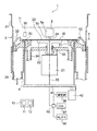
以下、図1乃至図4を参照して本発明の実施の形態について説明する。
ここで図1は、本発明による基板処理装置を示す縦断面図である。図1に示すように基板処理装置1は基板であるウエハWの中央近傍を、被処理面が上を向くようにほぼ水平な状態で吸着保持すると共に、当該ウエハWを鉛直軸まわりに回転させ、かつ昇降させるための、例えばポリテトラフルオロエチレンやポリエ−テルエ−テルケトン等の樹脂あるいは金属により構成されたウエハ保持部(基板保持機構)22と、このウエハ保持部22の上方に配置され、ウエハ保持部22により吸着保持されたウエハW表面に薬液、DIW(De Inoized Water)等からなる処理液、あるいはN2ガス等の乾燥ガスを供給するノズル(処理流体供給部)5とを備えている。このうち、ウエハ保持部22は基板保持機構をなすものであって、ウエハWを保持する保持面23と、保持面23の中央部に開口し、ウエハWを真空吸着する開口(吸引部)24とを有している。そしてこのウエハ保持部22は昇降機構とモ−タとが組み合わされた駆動部21により、回転軸を介して鉛直軸まわりに回転自在かつ昇降自在となっている。こうしてウエハWは、ウエハ保持部22により、図1に示すウエハ保持部22に吸着保持された処理位置と、処理位置よりも上方側のウエハWの受け渡し位置Hとの間で昇降自在、回転自在に保持される。
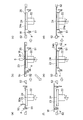
まず、図5に示すように、ノズル(塗布液供給部)50を退避位置から保持面23の例えば周縁部の上方位置に移動させ、ウエハ保持部22を回転させながら、ウエハ保持部22の保持面23の周縁部にノズル(塗布液供給部)50から塗布液50aを供給する。
このためウエハWを清浄に保ちならが、ウエハWに対して液処理を施すことができる。
このため、開口24から噴出されたDIW24aはウエハW裏面を通って外方へ流出する。
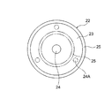
次に本発明の変形例について述べる。上記実施の形態において、保持面23上に環状塗布膜25を形成した後、保持面23の中央部に設けられた開口24からDIW24aを保持面23に供給して環状塗布膜25を溶解またはエッチングして除去する例を示したが、これに限らず保持面23の周縁部にDIWを供給する3個の開口24Aを設けてもよい(図4参照)。この場合、保持面23の中央部の開口24は真空源56に接続されて吸引部として機能する。また周縁部の開口24Aは、DIW供給源57またはN2ガス供給源58に選択的に接続されてDIW供給部あるいはN2ガス供給部として機能する。
3 カップ
4 保持ピン
5 ノズル
5a 処理流体
10 制御部
11 記憶媒体
22 ウエハ保持部
23 保持面
24 開口
24a DIW
24b N2ガス
25 環状塗布膜
31 外カップ
32 内カップ
42 昇降機構
50 ノズル
50a 塗布液
51 塗布液カップ
52 リングガイド
W ウエハ
Claims (16)
- 保持面と、この保持面に設けられた吸引部とを有する基板保持機構と、
前記基板保持機構の保持面に設けられた前記吸引部を囲うように塗布液を供給して、前記保持面に基板を載置する環状塗布膜を形成する塗布液供給部と、を備えたことを特徴とする基板処理装置。 - 前記基板保持部は、回転自在であることを特徴とする請求項1記載の基板処理装置。
- 前記保持面上の前記環状塗布膜を溶解またはエッチングする処理液を供給する塗布膜処理液供給部を更に備えたことを特徴とする請求項1記載の基板処理装置。
- 前記基板保持機構の外周に、前記基板保持機構に保持された基板を上方へ持上げる保持ピンを設けたことを特徴とする請求項1乃至3のいずれか記載の基板処理装置。
- 前記基板保持機構の外周に、前記基板保持機構に保持された基板の周縁部を保持して持上げるリングガイドを設けたことを特徴とする請求項1乃至4のいずれか記載の基板処理装置。
- 前記基板保持機構と前記保持ピンとの間に、前記基板保持機構の保持面周縁部に供給された塗布液を下方へ導く塗布液カップを設けたことを特徴とする請求項4または5記載の基板処理装置。
- 基板保持機構の上方に、前記基板保持機構に保持された基板に対して処理流体を供給する処理流体供給部を設けたことを特徴とする請求項1乃至6のいずれか記載の基板処理装置。
- 保持面と、この保持面に設けられた吸引部とを有する基板保持機構を準備する工程と、
前記基板保持機構の保持面に設けられた前記吸引部を囲うように塗布液供給部から塗布液を供給して、前記保持面に基板を載置する環状塗布膜を形成する工程と、
前記保持面の前記環状塗布膜上に基板を載置して基板を吸引部により吸着保持する工程と、を備えたことを特徴とする基板処理方法。 - 前記基板保持機構は、回転自在であることを特徴とする請求項8の基板処理方法。
- 前記基板保持機構により保持された基板上に、前記基板保持機構の上方に設けられた処理流体供給部から処理流体を供給する工程を更に備えたことを特徴とする請求項8または9記載の基板処理方法。
- 前記保持面の周縁部に塗布液を供給する際、前記基板保持機構外周に設けられた塗布液カップにより塗布液を下方へ導くことを特徴とする請求項8乃至10のいずれか記載の基板処理方法。
- 前記保持面上の前記環状塗布膜を溶解またはエッチングする処理液を塗布膜処理液供給部から供給することを特徴とする請求項8乃至11のいずれか記載の基板処理方法。
- 前記基板保持機構の外周に設けられたリングガイドにより、前記基板保持機構に保持された基板の周縁部を保持して持上げることを特徴とする請求項12記載の基板処理方法。
- 前記塗布液は溶剤と残部とを含み、前記保持面に供給された後、溶剤が外方へ放出され、残部が前記保持面上に残ることを特徴とする請求項8乃至13のいずれか記載の基板処理方法。
- 前記塗布液はトップコート液、レジスト液または反射防止膜液のいずれかを含むことを特徴とする請求項14記載の基板処理方法。
- コンピュータに基板処理方法を実行させるための記憶媒体において、
前記基板処理方法は、
保持面と、この保持面に設けられた吸引部とを有する基板保持機構を準備する工程と、
前記基板保持機構の保持面に設けられた前記吸引部を囲うように塗布液供給部から塗布液を供給して、前記保持面に基板を載置する環状塗布膜を形成する工程と、
前記保持面の前記環状塗布膜上に基板を載置して基板を吸引部により吸着保持する工程と、を備えたことを特徴とする記憶媒体。
Priority Applications (4)
| Application Number | Priority Date | Filing Date | Title |
|---|---|---|---|
| JP2015125695A JP6373803B2 (ja) | 2015-06-23 | 2015-06-23 | 基板処理装置、基板処理方法および記憶媒体 |
| TW105118576A TWI649831B (zh) | 2015-06-23 | 2016-06-14 | Substrate processing device, substrate processing method, and memory medium |
| US15/187,965 US20160375462A1 (en) | 2015-06-23 | 2016-06-21 | Substrate processing apparatus, substrate processing method, and recording medium |
| KR1020160077389A KR102508316B1 (ko) | 2015-06-23 | 2016-06-21 | 기판 처리 장치, 기판 처리 방법 및 기억 매체 |
Applications Claiming Priority (1)
| Application Number | Priority Date | Filing Date | Title |
|---|---|---|---|
| JP2015125695A JP6373803B2 (ja) | 2015-06-23 | 2015-06-23 | 基板処理装置、基板処理方法および記憶媒体 |
Publications (2)
| Publication Number | Publication Date |
|---|---|
| JP2017011122A true JP2017011122A (ja) | 2017-01-12 |
| JP6373803B2 JP6373803B2 (ja) | 2018-08-15 |
Family
ID=57601773
Family Applications (1)
| Application Number | Title | Priority Date | Filing Date |
|---|---|---|---|
| JP2015125695A Active JP6373803B2 (ja) | 2015-06-23 | 2015-06-23 | 基板処理装置、基板処理方法および記憶媒体 |
Country Status (4)
| Country | Link |
|---|---|
| US (1) | US20160375462A1 (ja) |
| JP (1) | JP6373803B2 (ja) |
| KR (1) | KR102508316B1 (ja) |
| TW (1) | TWI649831B (ja) |
Cited By (1)
| Publication number | Priority date | Publication date | Assignee | Title |
|---|---|---|---|---|
| JP2018175322A (ja) * | 2017-04-12 | 2018-11-15 | 株式会社三共 | 遊技機 |
Families Citing this family (2)
| Publication number | Priority date | Publication date | Assignee | Title |
|---|---|---|---|---|
| DE102015104735A1 (de) * | 2015-03-27 | 2016-09-29 | Obducat Ab | Drehteller zur Aufnahme eines Substrats für eine Belackungsvorrichtung |
| TWI831656B (zh) * | 2018-01-04 | 2024-02-01 | 日商東京威力科創股份有限公司 | 基板處理裝置及基板處理方法 |
Citations (10)
| Publication number | Priority date | Publication date | Assignee | Title |
|---|---|---|---|---|
| JP2002343696A (ja) * | 2001-05-11 | 2002-11-29 | Tokyo Electron Ltd | 基板の処理装置 |
| US20030047283A1 (en) * | 2001-09-10 | 2003-03-13 | Applied Materials, Inc. | Apparatus for supporting a substrate and method of fabricating same |
| JP2006100514A (ja) * | 2004-09-29 | 2006-04-13 | Dainippon Screen Mfg Co Ltd | 除去装置、保護膜形成装置、基板処理システム、および除去方法 |
| JP2008091353A (ja) * | 2006-09-07 | 2008-04-17 | Ngk Insulators Ltd | 静電チャック |
| US20080226830A1 (en) * | 2006-08-31 | 2008-09-18 | Sokudo Co., Ltd. | Method and system for removal of films from peripheral portions of a substrate |
| JP2010034219A (ja) * | 2008-07-28 | 2010-02-12 | Sokudo Co Ltd | 基板処理ユニットおよび基板処理装置 |
| JP2010135443A (ja) * | 2008-12-02 | 2010-06-17 | Tanken Seal Seiko Co Ltd | 真空吸着パッドおよび真空吸着装置 |
| JP2010219190A (ja) * | 2009-03-16 | 2010-09-30 | Dainippon Printing Co Ltd | 薄膜形成装置及び薄膜形成方法 |
| JP2010239026A (ja) * | 2009-03-31 | 2010-10-21 | Tokyo Electron Ltd | 基板保持部材及び液処理装置 |
| WO2014084060A1 (ja) * | 2012-11-28 | 2014-06-05 | 京セラ株式会社 | 載置用部材およびその製造方法 |
Family Cites Families (37)
| Publication number | Priority date | Publication date | Assignee | Title |
|---|---|---|---|---|
| US4544446A (en) * | 1984-07-24 | 1985-10-01 | J. T. Baker Chemical Co. | VLSI chemical reactor |
| US5580607A (en) * | 1991-07-26 | 1996-12-03 | Tokyo Electron Limited | Coating apparatus and method |
| EP0669644B1 (en) * | 1994-02-28 | 1997-08-20 | Applied Materials, Inc. | Electrostatic chuck |
| US5558111A (en) * | 1995-02-02 | 1996-09-24 | International Business Machines Corporation | Apparatus and method for carrier backing film reconditioning |
| JP3265238B2 (ja) * | 1997-08-01 | 2002-03-11 | 東京エレクトロン株式会社 | 液膜形成装置及びその方法 |
| JP3333733B2 (ja) * | 1998-02-20 | 2002-10-15 | 東京エレクトロン株式会社 | 洗浄装置 |
| US20010001384A1 (en) * | 1998-07-29 | 2001-05-24 | Takeshi Arai | Silicon epitaxial wafer and production method therefor |
| US6305677B1 (en) * | 1999-03-30 | 2001-10-23 | Lam Research Corporation | Perimeter wafer lifting |
| KR100585448B1 (ko) * | 1999-04-08 | 2006-06-02 | 동경 엘렉트론 주식회사 | 막 형성방법 및 막 형성장치 |
| US6312171B1 (en) * | 1999-08-12 | 2001-11-06 | Tokyo Electron Limited | Developing apparatus and method thereof |
| JP2001276715A (ja) * | 2000-03-31 | 2001-10-09 | Tokyo Electron Ltd | 塗布装置及び塗布方法 |
| US7451774B2 (en) * | 2000-06-26 | 2008-11-18 | Applied Materials, Inc. | Method and apparatus for wafer cleaning |
| AU2001270205A1 (en) * | 2000-06-26 | 2002-01-08 | Applied Materials, Inc. | Method and apparatus for wafer cleaning |
| JP4094262B2 (ja) * | 2001-09-13 | 2008-06-04 | 住友大阪セメント株式会社 | 吸着固定装置及びその製造方法 |
| TWI261875B (en) * | 2002-01-30 | 2006-09-11 | Tokyo Electron Ltd | Processing apparatus and substrate processing method |
| US20040084144A1 (en) * | 2002-08-21 | 2004-05-06 | Dainippon Screen Mfg. Co., Ltd. | Substrate processing apparatus and substrate processing method |
| JP2004306191A (ja) * | 2003-04-07 | 2004-11-04 | Seiko Epson Corp | テーブル装置、成膜装置、光学素子、半導体素子及び電子機器 |
| US7442285B2 (en) * | 2004-06-17 | 2008-10-28 | Vapor Technologies, Inc. | Common rack for electroplating and PVD coating operations |
| KR101323213B1 (ko) * | 2005-07-13 | 2013-10-30 | 후지필름 디마틱스, 인크. | 유체 증착 장치 |
| JP4707593B2 (ja) * | 2006-03-23 | 2011-06-22 | 大日本スクリーン製造株式会社 | 熱処理装置と基板吸着方法 |
| TWI352628B (en) * | 2006-07-21 | 2011-11-21 | Akrion Technologies Inc | Nozzle for use in the megasonic cleaning of substr |
| US8852349B2 (en) * | 2006-09-15 | 2014-10-07 | Applied Materials, Inc. | Wafer processing hardware for epitaxial deposition with reduced auto-doping and backside defects |
| KR20090107514A (ko) * | 2006-12-26 | 2009-10-13 | 후지필름 디마틱스, 인크. | 전도성 요소를 구비한 인쇄 시스템 |
| JP5065071B2 (ja) * | 2007-03-15 | 2012-10-31 | 東京エレクトロン株式会社 | 塗布処理方法、塗布処理装置及びコンピュータ読み取り可能な記憶媒体 |
| US8057602B2 (en) * | 2007-05-09 | 2011-11-15 | Applied Materials, Inc. | Apparatus and method for supporting, positioning and rotating a substrate in a processing chamber |
| US7989022B2 (en) * | 2007-07-20 | 2011-08-02 | Micron Technology, Inc. | Methods of processing substrates, electrostatic carriers for retaining substrates for processing, and assemblies comprising electrostatic carriers having substrates electrostatically bonded thereto |
| JP2009088244A (ja) * | 2007-09-28 | 2009-04-23 | Tokyo Electron Ltd | 基板クリーニング装置、基板処理装置、基板クリーニング方法、基板処理方法及び記憶媒体 |
| JP4601079B2 (ja) * | 2007-12-17 | 2010-12-22 | 東京エレクトロン株式会社 | 基板処理方法及び基板処理装置 |
| JP5312923B2 (ja) * | 2008-01-31 | 2013-10-09 | 大日本スクリーン製造株式会社 | 基板処理装置 |
| JP5413016B2 (ja) * | 2008-07-31 | 2014-02-12 | 東京エレクトロン株式会社 | 基板の洗浄方法、基板の洗浄装置及び記憶媒体 |
| JP5401255B2 (ja) * | 2008-11-05 | 2014-01-29 | 東京エレクトロン株式会社 | 洗浄装置、洗浄方法、および記憶媒体 |
| EP2975017B1 (en) * | 2009-09-11 | 2017-11-08 | Ricoh Company, Ltd. | Leaving substituent-containing compound, organic semiconductor material, organic semiconductor film containing the material, organic electronic device containing the film, method for producing film-like product, pi-electron conjugated compound and method for producing the pi-electron conjugated compound |
| JP5270607B2 (ja) * | 2010-03-30 | 2013-08-21 | 大日本スクリーン製造株式会社 | 基板処理装置 |
| JP5666183B2 (ja) * | 2010-07-20 | 2015-02-12 | ルネサスエレクトロニクス株式会社 | 半導体装置の製造方法 |
| JP5586734B2 (ja) * | 2012-08-07 | 2014-09-10 | 東京エレクトロン株式会社 | 基板洗浄装置、基板洗浄システム、基板洗浄方法および記憶媒体 |
| JP6283532B2 (ja) * | 2014-02-26 | 2018-02-21 | 東京エレクトロン株式会社 | 静電チャックの製造方法 |
| US9209062B1 (en) * | 2014-05-28 | 2015-12-08 | Spintrac Systems, Inc. | Removable spin chamber with vacuum attachment |
-
2015
- 2015-06-23 JP JP2015125695A patent/JP6373803B2/ja active Active
-
2016
- 2016-06-14 TW TW105118576A patent/TWI649831B/zh active
- 2016-06-21 KR KR1020160077389A patent/KR102508316B1/ko active Active
- 2016-06-21 US US15/187,965 patent/US20160375462A1/en not_active Abandoned
Patent Citations (10)
| Publication number | Priority date | Publication date | Assignee | Title |
|---|---|---|---|---|
| JP2002343696A (ja) * | 2001-05-11 | 2002-11-29 | Tokyo Electron Ltd | 基板の処理装置 |
| US20030047283A1 (en) * | 2001-09-10 | 2003-03-13 | Applied Materials, Inc. | Apparatus for supporting a substrate and method of fabricating same |
| JP2006100514A (ja) * | 2004-09-29 | 2006-04-13 | Dainippon Screen Mfg Co Ltd | 除去装置、保護膜形成装置、基板処理システム、および除去方法 |
| US20080226830A1 (en) * | 2006-08-31 | 2008-09-18 | Sokudo Co., Ltd. | Method and system for removal of films from peripheral portions of a substrate |
| JP2008091353A (ja) * | 2006-09-07 | 2008-04-17 | Ngk Insulators Ltd | 静電チャック |
| JP2010034219A (ja) * | 2008-07-28 | 2010-02-12 | Sokudo Co Ltd | 基板処理ユニットおよび基板処理装置 |
| JP2010135443A (ja) * | 2008-12-02 | 2010-06-17 | Tanken Seal Seiko Co Ltd | 真空吸着パッドおよび真空吸着装置 |
| JP2010219190A (ja) * | 2009-03-16 | 2010-09-30 | Dainippon Printing Co Ltd | 薄膜形成装置及び薄膜形成方法 |
| JP2010239026A (ja) * | 2009-03-31 | 2010-10-21 | Tokyo Electron Ltd | 基板保持部材及び液処理装置 |
| WO2014084060A1 (ja) * | 2012-11-28 | 2014-06-05 | 京セラ株式会社 | 載置用部材およびその製造方法 |
Cited By (1)
| Publication number | Priority date | Publication date | Assignee | Title |
|---|---|---|---|---|
| JP2018175322A (ja) * | 2017-04-12 | 2018-11-15 | 株式会社三共 | 遊技機 |
Also Published As
| Publication number | Publication date |
|---|---|
| US20160375462A1 (en) | 2016-12-29 |
| TWI649831B (zh) | 2019-02-01 |
| KR20170000348A (ko) | 2017-01-02 |
| KR102508316B1 (ko) | 2023-03-10 |
| JP6373803B2 (ja) | 2018-08-15 |
| TW201724335A (zh) | 2017-07-01 |
Similar Documents
| Publication | Publication Date | Title |
|---|---|---|
| KR100979979B1 (ko) | 액처리 장치 및 액처리 방법 | |
| JP6118758B2 (ja) | 基板処理装置及び基板処理方法並びに基板処理プログラムを記録したコンピュータ読み取り可能な記録媒体 | |
| JP6992131B2 (ja) | 基板洗浄装置、基板処理装置、基板洗浄方法および基板処理方法 | |
| JP7073658B2 (ja) | 基板処理方法、基板処理装置、及び記憶媒体 | |
| KR100907125B1 (ko) | 기판처리방법 및 기판처리장치 | |
| CN107026109A (zh) | 基板清洗装置及方法、基板处理装置及方法 | |
| TW201628114A (zh) | 液處理方法、記憶媒體及液處理裝置 | |
| CN101236889B (zh) | 基板处理装置以及基板处理方法 | |
| CN117642846A (zh) | 基板清洗装置 | |
| JP6373803B2 (ja) | 基板処理装置、基板処理方法および記憶媒体 | |
| TWI708641B (zh) | 基板處理方法 | |
| JP2019145687A (ja) | 洗浄具、基板洗浄装置及び基板洗浄方法 | |
| US20180269079A1 (en) | Substrate treatment method and substrate treatment device | |
| JP6411571B2 (ja) | 基板処理装置及び基板処理方法並びに基板処理プログラムを記録したコンピュータ読み取り可能な記録媒体 | |
| CN117732765A (zh) | 下表面刷、刷单元及基板清洗装置 | |
| JP6101023B2 (ja) | 基板処理装置および基板処理方法 | |
| US12246358B2 (en) | Substrate cleaning apparatus and substrate cleaning method | |
| US20240091816A1 (en) | Substrate cleaning apparatus and substrate cleaning method | |
| KR20100048407A (ko) | 기판 지지 부재 및 이를 구비하는 기판 처리 장치 | |
| JP3387730B2 (ja) | 回転式基板処理装置 | |
| JP2024072489A (ja) | 基板処理方法および基板処理システム | |
| JP2012204483A (ja) | 基板処理方法及び基板処理装置 |
Legal Events
| Date | Code | Title | Description |
|---|---|---|---|
| A621 | Written request for application examination |
Free format text: JAPANESE INTERMEDIATE CODE: A621 Effective date: 20170809 |
|
| TRDD | Decision of grant or rejection written | ||
| A01 | Written decision to grant a patent or to grant a registration (utility model) |
Free format text: JAPANESE INTERMEDIATE CODE: A01 Effective date: 20180619 |
|
| A977 | Report on retrieval |
Free format text: JAPANESE INTERMEDIATE CODE: A971007 Effective date: 20180620 |
|
| A61 | First payment of annual fees (during grant procedure) |
Free format text: JAPANESE INTERMEDIATE CODE: A61 Effective date: 20180718 |
|
| R150 | Certificate of patent or registration of utility model |
Ref document number: 6373803 Country of ref document: JP Free format text: JAPANESE INTERMEDIATE CODE: R150 |
|
| R250 | Receipt of annual fees |
Free format text: JAPANESE INTERMEDIATE CODE: R250 |
|
| R250 | Receipt of annual fees |
Free format text: JAPANESE INTERMEDIATE CODE: R250 |
|
| R250 | Receipt of annual fees |
Free format text: JAPANESE INTERMEDIATE CODE: R250 |
|
| R250 | Receipt of annual fees |
Free format text: JAPANESE INTERMEDIATE CODE: R250 |
|
| R250 | Receipt of annual fees |
Free format text: JAPANESE INTERMEDIATE CODE: R250 |