JP2017011167A - エッチング方法 - Google Patents
エッチング方法 Download PDFInfo
- Publication number
- JP2017011167A JP2017011167A JP2015126710A JP2015126710A JP2017011167A JP 2017011167 A JP2017011167 A JP 2017011167A JP 2015126710 A JP2015126710 A JP 2015126710A JP 2015126710 A JP2015126710 A JP 2015126710A JP 2017011167 A JP2017011167 A JP 2017011167A
- Authority
- JP
- Japan
- Prior art keywords
- gas
- region
- sequence
- high frequency
- plasma
- Prior art date
- Legal status (The legal status is an assumption and is not a legal conclusion. Google has not performed a legal analysis and makes no representation as to the accuracy of the status listed.)
- Granted
Links
Images


Classifications
-
- H—ELECTRICITY
- H10—SEMICONDUCTOR DEVICES; ELECTRIC SOLID-STATE DEVICES NOT OTHERWISE PROVIDED FOR
- H10P—GENERIC PROCESSES OR APPARATUS FOR THE MANUFACTURE OR TREATMENT OF DEVICES COVERED BY CLASS H10
- H10P50/00—Etching of wafers, substrates or parts of devices
- H10P50/20—Dry etching; Plasma etching; Reactive-ion etching
- H10P50/24—Dry etching; Plasma etching; Reactive-ion etching of semiconductor materials
- H10P50/242—Dry etching; Plasma etching; Reactive-ion etching of semiconductor materials of Group IV materials
-
- H—ELECTRICITY
- H10—SEMICONDUCTOR DEVICES; ELECTRIC SOLID-STATE DEVICES NOT OTHERWISE PROVIDED FOR
- H10P—GENERIC PROCESSES OR APPARATUS FOR THE MANUFACTURE OR TREATMENT OF DEVICES COVERED BY CLASS H10
- H10P50/00—Etching of wafers, substrates or parts of devices
- H10P50/20—Dry etching; Plasma etching; Reactive-ion etching
- H10P50/28—Dry etching; Plasma etching; Reactive-ion etching of insulating materials
- H10P50/282—Dry etching; Plasma etching; Reactive-ion etching of insulating materials of inorganic materials
- H10P50/283—Dry etching; Plasma etching; Reactive-ion etching of insulating materials of inorganic materials by chemical means
-
- H—ELECTRICITY
- H05—ELECTRIC TECHNIQUES NOT OTHERWISE PROVIDED FOR
- H05H—PLASMA TECHNIQUE; PRODUCTION OF ACCELERATED ELECTRICALLY-CHARGED PARTICLES OR OF NEUTRONS; PRODUCTION OR ACCELERATION OF NEUTRAL MOLECULAR OR ATOMIC BEAMS
- H05H1/00—Generating plasma; Handling plasma
- H05H1/24—Generating plasma
- H05H1/46—Generating plasma using applied electromagnetic fields, e.g. high frequency or microwave energy
-
- H—ELECTRICITY
- H10—SEMICONDUCTOR DEVICES; ELECTRIC SOLID-STATE DEVICES NOT OTHERWISE PROVIDED FOR
- H10P—GENERIC PROCESSES OR APPARATUS FOR THE MANUFACTURE OR TREATMENT OF DEVICES COVERED BY CLASS H10
- H10P14/00—Formation of materials, e.g. in the shape of layers or pillars
- H10P14/60—Formation of materials, e.g. in the shape of layers or pillars of insulating materials
- H10P14/65—Formation of materials, e.g. in the shape of layers or pillars of insulating materials characterised by treatments performed before or after the formation of the materials
- H10P14/6502—Formation of materials, e.g. in the shape of layers or pillars of insulating materials characterised by treatments performed before or after the formation of the materials of treatments performed before formation of the materials
- H10P14/6512—Formation of materials, e.g. in the shape of layers or pillars of insulating materials characterised by treatments performed before or after the formation of the materials of treatments performed before formation of the materials by exposure to a gas or vapour
- H10P14/6514—Formation of materials, e.g. in the shape of layers or pillars of insulating materials characterised by treatments performed before or after the formation of the materials of treatments performed before formation of the materials by exposure to a gas or vapour by exposure to a plasma
-
- H—ELECTRICITY
- H10—SEMICONDUCTOR DEVICES; ELECTRIC SOLID-STATE DEVICES NOT OTHERWISE PROVIDED FOR
- H10P—GENERIC PROCESSES OR APPARATUS FOR THE MANUFACTURE OR TREATMENT OF DEVICES COVERED BY CLASS H10
- H10P50/00—Etching of wafers, substrates or parts of devices
- H10P50/20—Dry etching; Plasma etching; Reactive-ion etching
- H10P50/26—Dry etching; Plasma etching; Reactive-ion etching of conductive or resistive materials
- H10P50/264—Dry etching; Plasma etching; Reactive-ion etching of conductive or resistive materials by chemical means
- H10P50/266—Dry etching; Plasma etching; Reactive-ion etching of conductive or resistive materials by chemical means by vapour etching only
- H10P50/267—Dry etching; Plasma etching; Reactive-ion etching of conductive or resistive materials by chemical means by vapour etching only using plasmas
-
- H—ELECTRICITY
- H10—SEMICONDUCTOR DEVICES; ELECTRIC SOLID-STATE DEVICES NOT OTHERWISE PROVIDED FOR
- H10P—GENERIC PROCESSES OR APPARATUS FOR THE MANUFACTURE OR TREATMENT OF DEVICES COVERED BY CLASS H10
- H10P50/00—Etching of wafers, substrates or parts of devices
- H10P50/20—Dry etching; Plasma etching; Reactive-ion etching
- H10P50/28—Dry etching; Plasma etching; Reactive-ion etching of insulating materials
- H10P50/282—Dry etching; Plasma etching; Reactive-ion etching of insulating materials of inorganic materials
- H10P50/283—Dry etching; Plasma etching; Reactive-ion etching of insulating materials of inorganic materials by chemical means
- H10P50/285—Dry etching; Plasma etching; Reactive-ion etching of insulating materials of inorganic materials by chemical means of materials not containing Si, e.g. PZT or Al2O3
-
- H—ELECTRICITY
- H10—SEMICONDUCTOR DEVICES; ELECTRIC SOLID-STATE DEVICES NOT OTHERWISE PROVIDED FOR
- H10P—GENERIC PROCESSES OR APPARATUS FOR THE MANUFACTURE OR TREATMENT OF DEVICES COVERED BY CLASS H10
- H10P50/00—Etching of wafers, substrates or parts of devices
- H10P50/73—Etching of wafers, substrates or parts of devices using masks for insulating materials
-
- H—ELECTRICITY
- H10—SEMICONDUCTOR DEVICES; ELECTRIC SOLID-STATE DEVICES NOT OTHERWISE PROVIDED FOR
- H10W—GENERIC PACKAGES, INTERCONNECTIONS, CONNECTORS OR OTHER CONSTRUCTIONAL DETAILS OF DEVICES COVERED BY CLASS H10
- H10W20/00—Interconnections in chips, wafers or substrates
- H10W20/01—Manufacture or treatment
- H10W20/031—Manufacture or treatment of conductive parts of the interconnections
- H10W20/069—Manufacture or treatment of conductive parts of the interconnections by forming self-aligned vias or self-aligned contact plugs
-
- H—ELECTRICITY
- H10—SEMICONDUCTOR DEVICES; ELECTRIC SOLID-STATE DEVICES NOT OTHERWISE PROVIDED FOR
- H10W—GENERIC PACKAGES, INTERCONNECTIONS, CONNECTORS OR OTHER CONSTRUCTIONAL DETAILS OF DEVICES COVERED BY CLASS H10
- H10W20/00—Interconnections in chips, wafers or substrates
- H10W20/01—Manufacture or treatment
- H10W20/071—Manufacture or treatment of dielectric parts thereof
- H10W20/074—Manufacture or treatment of dielectric parts thereof of dielectric parts comprising thin functional dielectric layers, e.g. dielectric etch-stop, barrier, capping or liner layers
- H10W20/076—Manufacture or treatment of dielectric parts thereof of dielectric parts comprising thin functional dielectric layers, e.g. dielectric etch-stop, barrier, capping or liner layers in via holes or trenches
- H10W20/0765—Manufacture or treatment of dielectric parts thereof of dielectric parts comprising thin functional dielectric layers, e.g. dielectric etch-stop, barrier, capping or liner layers in via holes or trenches the thin functional dielectric layers being temporary, e.g. sacrificial layers
Landscapes
- Physics & Mathematics (AREA)
- Engineering & Computer Science (AREA)
- Plasma & Fusion (AREA)
- Electromagnetism (AREA)
- Spectroscopy & Molecular Physics (AREA)
- Drying Of Semiconductors (AREA)
Abstract
Description
・処理容器内圧力:10mTorr(1.33Pa)〜50mTorr(6.65Pa)
・処理ガス
C4F8ガス:10sccm〜30sccm
CF4ガス:150sccm〜300sccm
Arガス:200sccm〜500sccm
・プラズマ生成用の高周波の電力:300W〜1000W
・高周波バイアスの電力:200W〜500W
・処理容器内圧力:50mTorr(6.65Pa)〜200mTorr(26.6Pa)
・処理ガス
N2ガス:200sccm〜400sccm
H2ガス:200sccm〜400sccm
・プラズマ生成用の高周波の電力:500W〜2000W
・高周波バイアスの電力:200W〜500W
・処理容器内圧力:10mTorr(1.33Pa)〜50mTorr(6.65Pa)
・処理ガス
C4F8ガス:10sccm〜30sccm
CF4ガス:50sccm〜150sccm
Arガス:500sccm〜1000sccm
O2ガス:10sccm〜30sccm
・プラズマ生成用の高周波の電力:500W〜2000W
・高周波バイアスの電力:500W〜2000W
・処理容器内圧力:30mTorr(3.99Pa)〜200mTorr(26.6Pa)
・処理ガス
O2ガス:50sccm〜500sccm
Arガス:200sccm〜1500sccm
・プラズマ生成用の高周波の電力:100W〜500W
・高周波バイアスの電力:0W〜200W
・処理容器内圧力:10mTorr(1.33Pa)〜50mTorr(6.65Pa)
・処理ガス
C4F6ガス:2sccm〜10sccm
Arガス:500sccm〜1500sccm
・プラズマ生成用の高周波の電力:100W〜500W
・高周波バイアスの電力:0W〜50W
・処理容器内圧力:10mTorr(1.33Pa)〜50mTorr(6.65Pa)
・処理ガス
O2ガス:2sccm〜20sccm
Arガス:500sccm〜1500sccm
・プラズマ生成用の高周波の電力:100W〜500W
・高周波バイアスの電力:0W
・処理容器内圧力:10mTorr(1.33Pa)〜50mTorr(6.65Pa)
・処理ガス
Arガス:500sccm〜1500sccm
・プラズマ生成用の高周波の電力:100W〜500W
・高周波バイアスの電力:20W〜300W
・処理容器内圧力:10mTorr(1.33Pa)〜50mTorr(6.65Pa)
・処理ガス
C4F6ガス:2sccm〜10sccm
Arガス:500sccm〜1500sccm
・プラズマ生成用の高周波の電力:100W〜700W
・高周波バイアスの電力:0W〜50W
・処理容器内圧力:40mTorr(5.33Pa)〜120mTorr(16.0Pa)
・処理ガス
O2ガス:0.1sccm〜20sccm
Arガス:10sccm〜500sccm
・プラズマ生成用の高周波の電力:25W〜100W
・高周波バイアスの電力:0W〜25W
・処理容器内圧力:10mTorr(1.33Pa)〜50mTorr(6.65Pa)
・処理ガス
C4F6ガス:2sccm〜10sccm
Arガス:500sccm〜2000sccm
O2ガス:2sccm〜20sccm
・プラズマ生成用の高周波電力:100W〜500W
・高周波バイアス電力:20W〜300W
・電源70の電圧:0V〜900V
<工程ST11>
処理容器12内の空間の圧力:20sccm(2.66Pa)
C4F6ガス流量:4sccm
Arガス流量:750sccm
プラズマ生成用の高周波:40MHz、300W
高周波バイアス:13MHz、50W
処理時間:10秒
<工程ST12>
処理容器12内の空間の圧力:80sccm(10.6Pa)
Arガス流量:100sccm
O2ガス流量:3sccm
プラズマ生成用の高周波:40MHz、50W
高周波バイアス:13MHz、0W
処理時間:4秒
<工程ST13>
処理容器12内の空間の圧力:20sccm(2.66Pa)
Arガス流量:950sccm
プラズマ生成用の高周波:40MHz、500W
高周波バイアス:13MHz、50W
処理時間:4秒
<工程ST21>
処理容器12内の空間の圧力:20sccm(2.66Pa)
C4F6ガス流量:4sccm
Arガス流量:750sccm
プラズマ生成用の高周波:40MHz、500W
高周波バイアス:13MHz、0W
処理時間:10秒
<工程ST22>
処理容器12内の空間の圧力:80sccm(10.6Pa)
Arガス流量:100sccm
O2ガス流量:3sccm
プラズマ生成用の高周波:40MHz、50W
高周波バイアス:13MHz、0W
処理時間:4秒
Claims (5)
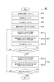
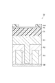
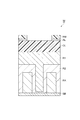
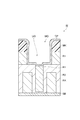
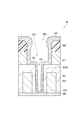
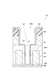
- 酸化シリコンから構成された第1領域を窒化シリコンから構成された第2領域に対して選択的にエッチングする方法であって、
前記第2領域は凹部を画成し、前記第1領域は前記凹部を埋め、且つ前記第2領域を覆うように設けられており、前記第1領域上にはマスクが設けられており、
該方法は、
前記第1領域をエッチングするために、第1シーケンスを一回以上実行する工程と、
前記第1領域を更にエッチングするために、第2シーケンスを一回以上実行する工程と、
を含み、
前記第1シーケンスが、
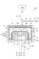
プラズマ処理装置の処理容器内においてフルオロカーボンガスを含む処理ガスのプラズマを生成する第1工程であり、前記第1領域及び前記第2領域を有する被処理体上にフルオロカーボンを含む堆積物を形成する、該第1工程と、
前記堆積物に含まれるフルオロカーボンのラジカルによって前記第1領域をエッチングする第2工程と、
を含み、
第2シーケンスを一回以上実行する前記工程は、第1シーケンスを一回以上実行する前記工程によって処理された前記被処理体に対して実行され、
前記第2シーケンスは、
前記処理容器内において、フルオロカーボンガスを含む処理ガスのプラズマを生成する第3工程であり、前記第1領域及び前記第2領域を有する被処理体上にフルオロカーボンを含む堆積物を形成する、該第3工程と、
前記処理容器内において酸素ガス及び不活性ガスを含む処理ガスのプラズマを生成する第4工程と、
を含む、方法。 - 前記第3工程において前記プラズマの生成のために使用される高周波の電力が、前記第1工程において前記プラズマの生成のために使用される高周波の電力より大きい、請求項1に記載の方法。
- 前記処理容器において前記被処理体は載置台上に載置され、
前記第4工程において設定される前記処理容器内の空間の圧力は、前記第1工程において設定される前記処理容器内の空間の圧力よりも高く、
前記第4工程において前記載置台に供給される高周波バイアスの電力が、前記第1工程において前記載置台に供給される高周波バイアスの電力よりも小さい、
請求項1又は2に記載の方法。 - 前記第1シーケンスは、前記処理容器内において酸素ガス及び不活性ガスを含む処理ガスのプラズマを生成する工程を更に含む、請求項1〜3の何れか一項に記載の方法。
- 第1シーケンスを一回以上実行する前記工程が、前記第2領域が露出するときを含む期間において実行され、
第1シーケンスを一回以上実行する前記工程と第2シーケンスを一回以上実行する前記工程との間において、前記処理容器内において生成したフルオロカーボンガスを含む処理ガスのプラズマにより前記第1領域を前記凹部の底までエッチングする工程を更に含む、請求項1〜4の何れか一項に記載の方法。
Priority Applications (4)
| Application Number | Priority Date | Filing Date | Title |
|---|---|---|---|
| JP2015126710A JP6550278B2 (ja) | 2015-06-24 | 2015-06-24 | エッチング方法 |
| US15/184,049 US9805945B2 (en) | 2015-06-24 | 2016-06-16 | Etching method |
| TW105119359A TWI692809B (zh) | 2015-06-24 | 2016-06-21 | 蝕刻方法 |
| KR1020160077811A KR102494293B1 (ko) | 2015-06-24 | 2016-06-22 | 에칭 방법 |
Applications Claiming Priority (1)
| Application Number | Priority Date | Filing Date | Title |
|---|---|---|---|
| JP2015126710A JP6550278B2 (ja) | 2015-06-24 | 2015-06-24 | エッチング方法 |
Publications (2)
| Publication Number | Publication Date |
|---|---|
| JP2017011167A true JP2017011167A (ja) | 2017-01-12 |
| JP6550278B2 JP6550278B2 (ja) | 2019-07-24 |
Family
ID=57602791
Family Applications (1)
| Application Number | Title | Priority Date | Filing Date |
|---|---|---|---|
| JP2015126710A Active JP6550278B2 (ja) | 2015-06-24 | 2015-06-24 | エッチング方法 |
Country Status (4)
| Country | Link |
|---|---|
| US (1) | US9805945B2 (ja) |
| JP (1) | JP6550278B2 (ja) |
| KR (1) | KR102494293B1 (ja) |
| TW (1) | TWI692809B (ja) |
Cited By (4)
| Publication number | Priority date | Publication date | Assignee | Title |
|---|---|---|---|---|
| JP2018157048A (ja) * | 2017-03-17 | 2018-10-04 | 株式会社日立ハイテクノロジーズ | エッチング方法及びプラズマ処理装置 |
| JP2019204950A (ja) * | 2018-05-11 | 2019-11-28 | 東京エレクトロン株式会社 | 酸化物の原子層エッチングの方法 |
| US11462416B2 (en) | 2019-02-04 | 2022-10-04 | Hitachi High-Tech Corporation | Plasma processing method and plasma processing apparatus |
| US12381071B2 (en) | 2020-09-17 | 2025-08-05 | Hitachi High-Tech Corporation | Plasma processing method and plasma processing apparatus |
Families Citing this family (5)
| Publication number | Priority date | Publication date | Assignee | Title |
|---|---|---|---|---|
| JP2016157793A (ja) * | 2015-02-24 | 2016-09-01 | 東京エレクトロン株式会社 | エッチング方法 |
| JP6861535B2 (ja) * | 2017-02-28 | 2021-04-21 | 東京エレクトロン株式会社 | 処理方法及びプラズマ処理装置 |
| US11527413B2 (en) * | 2021-01-29 | 2022-12-13 | Tokyo Electron Limited | Cyclic plasma etch process |
| US12347645B2 (en) * | 2021-04-27 | 2025-07-01 | Tokyo Electron Limited | Substrate processing method and substrate processing apparatus |
| JP2025076893A (ja) * | 2023-11-02 | 2025-05-16 | 株式会社Kokusai Electric | 基板処理方法、半導体装置の製造方法、基板処理装置、及びプログラム |
Citations (6)
| Publication number | Priority date | Publication date | Assignee | Title |
|---|---|---|---|---|
| JPH06260442A (ja) * | 1992-11-27 | 1994-09-16 | Mitsubishi Electric Corp | 半導体装置およびその製造方法 |
| JPH10256232A (ja) * | 1997-03-12 | 1998-09-25 | Nec Corp | 半導体装置の製造方法 |
| JP2000307001A (ja) * | 1999-04-22 | 2000-11-02 | Sony Corp | 半導体装置の製造方法 |
| JP2001068462A (ja) * | 1999-07-20 | 2001-03-16 | Samsung Electronics Co Ltd | 選択的ポリマー蒸着を用いたプラズマエッチング方法及びこれを用いたコンタクトホール形成方法 |
| US20050048789A1 (en) * | 2003-09-03 | 2005-03-03 | Merry Walter R. | Method for plasma etching a dielectric layer |
| JP2012204367A (ja) * | 2011-03-23 | 2012-10-22 | Tokyo Electron Ltd | 基板処理方法及び記憶媒体 |
Family Cites Families (4)
| Publication number | Priority date | Publication date | Assignee | Title |
|---|---|---|---|---|
| US6165910A (en) * | 1997-12-29 | 2000-12-26 | Lam Research Corporation | Self-aligned contacts for semiconductor device |
| US6174451B1 (en) * | 1998-03-27 | 2001-01-16 | Applied Materials, Inc. | Oxide etch process using hexafluorobutadiene and related unsaturated hydrofluorocarbons |
| US6716766B2 (en) * | 2002-08-22 | 2004-04-06 | Micron Technology, Inc. | Process variation resistant self aligned contact etch |
| US7708859B2 (en) | 2004-04-30 | 2010-05-04 | Lam Research Corporation | Gas distribution system having fast gas switching capabilities |
-
2015
- 2015-06-24 JP JP2015126710A patent/JP6550278B2/ja active Active
-
2016
- 2016-06-16 US US15/184,049 patent/US9805945B2/en active Active
- 2016-06-21 TW TW105119359A patent/TWI692809B/zh active
- 2016-06-22 KR KR1020160077811A patent/KR102494293B1/ko active Active
Patent Citations (6)
| Publication number | Priority date | Publication date | Assignee | Title |
|---|---|---|---|---|
| JPH06260442A (ja) * | 1992-11-27 | 1994-09-16 | Mitsubishi Electric Corp | 半導体装置およびその製造方法 |
| JPH10256232A (ja) * | 1997-03-12 | 1998-09-25 | Nec Corp | 半導体装置の製造方法 |
| JP2000307001A (ja) * | 1999-04-22 | 2000-11-02 | Sony Corp | 半導体装置の製造方法 |
| JP2001068462A (ja) * | 1999-07-20 | 2001-03-16 | Samsung Electronics Co Ltd | 選択的ポリマー蒸着を用いたプラズマエッチング方法及びこれを用いたコンタクトホール形成方法 |
| US20050048789A1 (en) * | 2003-09-03 | 2005-03-03 | Merry Walter R. | Method for plasma etching a dielectric layer |
| JP2012204367A (ja) * | 2011-03-23 | 2012-10-22 | Tokyo Electron Ltd | 基板処理方法及び記憶媒体 |
Cited By (6)
| Publication number | Priority date | Publication date | Assignee | Title |
|---|---|---|---|---|
| JP2018157048A (ja) * | 2017-03-17 | 2018-10-04 | 株式会社日立ハイテクノロジーズ | エッチング方法及びプラズマ処理装置 |
| US10665516B2 (en) | 2017-03-17 | 2020-05-26 | Hitachi High-Technologies Corporation | Etching method and plasma processing apparatus |
| JP2019204950A (ja) * | 2018-05-11 | 2019-11-28 | 東京エレクトロン株式会社 | 酸化物の原子層エッチングの方法 |
| JP7175237B2 (ja) | 2018-05-11 | 2022-11-18 | 東京エレクトロン株式会社 | 酸化物の原子層エッチングの方法 |
| US11462416B2 (en) | 2019-02-04 | 2022-10-04 | Hitachi High-Tech Corporation | Plasma processing method and plasma processing apparatus |
| US12381071B2 (en) | 2020-09-17 | 2025-08-05 | Hitachi High-Tech Corporation | Plasma processing method and plasma processing apparatus |
Also Published As
| Publication number | Publication date |
|---|---|
| JP6550278B2 (ja) | 2019-07-24 |
| US9805945B2 (en) | 2017-10-31 |
| TW201724252A (zh) | 2017-07-01 |
| KR20170000791A (ko) | 2017-01-03 |
| TWI692809B (zh) | 2020-05-01 |
| US20160379841A1 (en) | 2016-12-29 |
| KR102494293B1 (ko) | 2023-01-31 |
Similar Documents
| Publication | Publication Date | Title |
|---|---|---|
| JP6689674B2 (ja) | エッチング方法 | |
| US11205577B2 (en) | Method of selectively etching silicon oxide film on substrate | |
| JP6550278B2 (ja) | エッチング方法 | |
| KR102513051B1 (ko) | 에칭 방법 | |
| JP6592400B2 (ja) | エッチング方法 | |
| JP6521848B2 (ja) | エッチング方法 | |
| US11264246B2 (en) | Plasma etching method for selectively etching silicon oxide with respect to silicon nitride | |
| JP6578145B2 (ja) | エッチング方法 | |
| US9633864B2 (en) | Etching method | |
| US9754797B2 (en) | Etching method for selectively etching silicon oxide with respect to silicon nitride |
Legal Events
| Date | Code | Title | Description |
|---|---|---|---|
| A621 | Written request for application examination |
Free format text: JAPANESE INTERMEDIATE CODE: A621 Effective date: 20180511 |
|
| A131 | Notification of reasons for refusal |
Free format text: JAPANESE INTERMEDIATE CODE: A131 Effective date: 20190212 |
|
| A977 | Report on retrieval |
Free format text: JAPANESE INTERMEDIATE CODE: A971007 Effective date: 20190214 |
|
| A521 | Request for written amendment filed |
Free format text: JAPANESE INTERMEDIATE CODE: A523 Effective date: 20190405 |
|
| TRDD | Decision of grant or rejection written | ||
| A01 | Written decision to grant a patent or to grant a registration (utility model) |
Free format text: JAPANESE INTERMEDIATE CODE: A01 Effective date: 20190604 |
|
| A61 | First payment of annual fees (during grant procedure) |
Free format text: JAPANESE INTERMEDIATE CODE: A61 Effective date: 20190701 |
|
| R150 | Certificate of patent or registration of utility model |
Ref document number: 6550278 Country of ref document: JP Free format text: JAPANESE INTERMEDIATE CODE: R150 |
|
| R250 | Receipt of annual fees |
Free format text: JAPANESE INTERMEDIATE CODE: R250 |
|
| R250 | Receipt of annual fees |
Free format text: JAPANESE INTERMEDIATE CODE: R250 |
|
| R250 | Receipt of annual fees |
Free format text: JAPANESE INTERMEDIATE CODE: R250 |
|
| R250 | Receipt of annual fees |
Free format text: JAPANESE INTERMEDIATE CODE: R250 |