JP2017015923A - 液晶表示装置 - Google Patents
液晶表示装置 Download PDFInfo
- Publication number
- JP2017015923A JP2017015923A JP2015132414A JP2015132414A JP2017015923A JP 2017015923 A JP2017015923 A JP 2017015923A JP 2015132414 A JP2015132414 A JP 2015132414A JP 2015132414 A JP2015132414 A JP 2015132414A JP 2017015923 A JP2017015923 A JP 2017015923A
- Authority
- JP
- Japan
- Prior art keywords
- slit
- liquid crystal
- pixel
- tip
- electrode
- Prior art date
- Legal status (The legal status is an assumption and is not a legal conclusion. Google has not performed a legal analysis and makes no representation as to the accuracy of the status listed.)
- Granted
Links
Images




Classifications
-
- G—PHYSICS
- G02—OPTICS
- G02F—OPTICAL DEVICES OR ARRANGEMENTS FOR THE CONTROL OF LIGHT BY MODIFICATION OF THE OPTICAL PROPERTIES OF THE MEDIA OF THE ELEMENTS INVOLVED THEREIN; NON-LINEAR OPTICS; FREQUENCY-CHANGING OF LIGHT; OPTICAL LOGIC ELEMENTS; OPTICAL ANALOGUE/DIGITAL CONVERTERS
- G02F1/00—Devices or arrangements for the control of the intensity, colour, phase, polarisation or direction of light arriving from an independent light source, e.g. switching, gating or modulating; Non-linear optics
- G02F1/01—Devices or arrangements for the control of the intensity, colour, phase, polarisation or direction of light arriving from an independent light source, e.g. switching, gating or modulating; Non-linear optics for the control of the intensity, phase, polarisation or colour
- G02F1/13—Devices or arrangements for the control of the intensity, colour, phase, polarisation or direction of light arriving from an independent light source, e.g. switching, gating or modulating; Non-linear optics for the control of the intensity, phase, polarisation or colour based on liquid crystals, e.g. single liquid crystal display cells
- G02F1/133—Constructional arrangements; Operation of liquid crystal cells; Circuit arrangements
- G02F1/1333—Constructional arrangements; Manufacturing methods
- G02F1/1343—Electrodes
- G02F1/134309—Electrodes characterised by their geometrical arrangement
- G02F1/134363—Electrodes characterised by their geometrical arrangement for applying an electric field parallel to the substrate, i.e. in-plane switching [IPS]
-
- G—PHYSICS
- G02—OPTICS
- G02F—OPTICAL DEVICES OR ARRANGEMENTS FOR THE CONTROL OF LIGHT BY MODIFICATION OF THE OPTICAL PROPERTIES OF THE MEDIA OF THE ELEMENTS INVOLVED THEREIN; NON-LINEAR OPTICS; FREQUENCY-CHANGING OF LIGHT; OPTICAL LOGIC ELEMENTS; OPTICAL ANALOGUE/DIGITAL CONVERTERS
- G02F1/00—Devices or arrangements for the control of the intensity, colour, phase, polarisation or direction of light arriving from an independent light source, e.g. switching, gating or modulating; Non-linear optics
- G02F1/01—Devices or arrangements for the control of the intensity, colour, phase, polarisation or direction of light arriving from an independent light source, e.g. switching, gating or modulating; Non-linear optics for the control of the intensity, phase, polarisation or colour
- G02F1/13—Devices or arrangements for the control of the intensity, colour, phase, polarisation or direction of light arriving from an independent light source, e.g. switching, gating or modulating; Non-linear optics for the control of the intensity, phase, polarisation or colour based on liquid crystals, e.g. single liquid crystal display cells
- G02F1/133—Constructional arrangements; Operation of liquid crystal cells; Circuit arrangements
- G02F1/1333—Constructional arrangements; Manufacturing methods
- G02F1/1337—Surface-induced orientation of the liquid crystal molecules, e.g. by alignment layers
- G02F1/133707—Structures for producing distorted electric fields, e.g. bumps, protrusions, recesses, slits in pixel electrodes
-
- G—PHYSICS
- G02—OPTICS
- G02F—OPTICAL DEVICES OR ARRANGEMENTS FOR THE CONTROL OF LIGHT BY MODIFICATION OF THE OPTICAL PROPERTIES OF THE MEDIA OF THE ELEMENTS INVOLVED THEREIN; NON-LINEAR OPTICS; FREQUENCY-CHANGING OF LIGHT; OPTICAL LOGIC ELEMENTS; OPTICAL ANALOGUE/DIGITAL CONVERTERS
- G02F1/00—Devices or arrangements for the control of the intensity, colour, phase, polarisation or direction of light arriving from an independent light source, e.g. switching, gating or modulating; Non-linear optics
- G02F1/01—Devices or arrangements for the control of the intensity, colour, phase, polarisation or direction of light arriving from an independent light source, e.g. switching, gating or modulating; Non-linear optics for the control of the intensity, phase, polarisation or colour
- G02F1/13—Devices or arrangements for the control of the intensity, colour, phase, polarisation or direction of light arriving from an independent light source, e.g. switching, gating or modulating; Non-linear optics for the control of the intensity, phase, polarisation or colour based on liquid crystals, e.g. single liquid crystal display cells
- G02F1/133—Constructional arrangements; Operation of liquid crystal cells; Circuit arrangements
- G02F1/1333—Constructional arrangements; Manufacturing methods
- G02F1/1343—Electrodes
- G02F1/134309—Electrodes characterised by their geometrical arrangement
- G02F1/134372—Electrodes characterised by their geometrical arrangement for fringe field switching [FFS] where the common electrode is not patterned
Landscapes
- Physics & Mathematics (AREA)
- Nonlinear Science (AREA)
- Mathematical Physics (AREA)
- Chemical & Material Sciences (AREA)
- Crystallography & Structural Chemistry (AREA)
- General Physics & Mathematics (AREA)
- Optics & Photonics (AREA)
- Geometry (AREA)
- Spectroscopy & Molecular Physics (AREA)
- Liquid Crystal (AREA)
- Engineering & Computer Science (AREA)
- Microelectronics & Electronic Packaging (AREA)
Abstract
Description
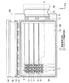
図1および図2は、本発明の実施の形態1に係る液晶表示装置を構成する液晶パネルの概略図である。図1は当該液晶パネルの全体を示した平面図、図2は、図1におけるA−B線に沿った断面図である。本実施の形態では、各画素のスイッチング素子として薄膜トランジスタ(Thin Film Transistor;TFT)を用いた横電界方式の液晶パネル、特にFFS方式の液晶パネルへ本発明を適用した場合の例を示す。
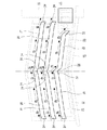
図6および図7は、実施の形態1に係る液晶パネルの画素の変形例を示す図である。図6は、アレイ基板10とカラーフィルタ基板20とが重ねられた状態における1画素の平面図であり、図7は、対向電極15に設けられた複数のスリット1(長スリット1Lおよび短スリット1S)の構成を示す平面図である。
図8は、本発明の実施の形態2に係る液晶表示装置を構成する液晶パネルの概略図である。実施の形態2の液晶表示装置の基本的構成は、実施の形態1と同様であるが、対向電極15に設けられるスリット1の延在方向が画素の行方向(X方向)となっている。先に述べたように、配向膜51a,51b(図2)の液晶配向方向(ラビング処理の方向)は、対向電極15のスリット1の延在方向に沿った方向にするため、実施の形態2では、X方向が液晶配向方向となる。
Claims (3)
- 液晶を挟持する2枚の基板うちの片方に形成された画素電極および対向電極を備え、
前記画素電極および前記対向電極のうちの少なくとも片方は、複数のスリットまたは電極を有しており、
前記複数のスリットまたは電極のうち、長さが比較的短いもののみに、先端を屈曲させた先端屈曲部が設けられている
ことを特徴とする液晶表示装置。 - 液晶を挟持する2枚の基板のうちの片方に形成された画素電極および対向電極を備え、
前記画素電極および前記対向電極のうちの少なくとも片方は、複数のスリットまたは電極を有しており、
前記複数のスリットまたは電極のそれぞれには、先端を屈曲させた先端屈曲部が設けられており、
前記複数のスリットまたは電極のうち、長さが比較的長いものに設けられた前記先端屈曲部の屈曲角度は、長さが比較的短いものに設けられた前記先端屈曲部の屈曲角度よりも大きい
ことを特徴とする液晶表示装置。 - 前記先端屈曲部の屈曲角度は、当該先端屈曲部が設けられたスリットまたは電極の長さが長いほど大きくなっている
請求項1または請求項2に記載の液晶表示装置。
Priority Applications (4)
| Application Number | Priority Date | Filing Date | Title |
|---|---|---|---|
| JP2015132414A JP6541474B2 (ja) | 2015-07-01 | 2015-07-01 | 液晶表示装置 |
| US15/168,734 US9869909B2 (en) | 2015-07-01 | 2016-05-31 | Liquid crystal display apparatus |
| DE102016211868.4A DE102016211868B4 (de) | 2015-07-01 | 2016-06-30 | Flüssigkristallanzeigevorrichtung |
| CN201610515892.8A CN106324921B (zh) | 2015-07-01 | 2016-07-01 | 液晶显示装置 |
Applications Claiming Priority (1)
| Application Number | Priority Date | Filing Date | Title |
|---|---|---|---|
| JP2015132414A JP6541474B2 (ja) | 2015-07-01 | 2015-07-01 | 液晶表示装置 |
Publications (3)
| Publication Number | Publication Date |
|---|---|
| JP2017015923A true JP2017015923A (ja) | 2017-01-19 |
| JP2017015923A5 JP2017015923A5 (ja) | 2018-07-26 |
| JP6541474B2 JP6541474B2 (ja) | 2019-07-10 |
Family
ID=57582926
Family Applications (1)
| Application Number | Title | Priority Date | Filing Date |
|---|---|---|---|
| JP2015132414A Active JP6541474B2 (ja) | 2015-07-01 | 2015-07-01 | 液晶表示装置 |
Country Status (4)
| Country | Link |
|---|---|
| US (1) | US9869909B2 (ja) |
| JP (1) | JP6541474B2 (ja) |
| CN (1) | CN106324921B (ja) |
| DE (1) | DE102016211868B4 (ja) |
Cited By (1)
| Publication number | Priority date | Publication date | Assignee | Title |
|---|---|---|---|---|
| JP2020140036A (ja) * | 2019-02-27 | 2020-09-03 | パナソニック液晶ディスプレイ株式会社 | 液晶表示パネル |
Families Citing this family (6)
| Publication number | Priority date | Publication date | Assignee | Title |
|---|---|---|---|---|
| CN105511177A (zh) * | 2016-02-02 | 2016-04-20 | 京东方科技集团股份有限公司 | 一种阵列基板和液晶显示装置 |
| CN108287441A (zh) * | 2018-02-08 | 2018-07-17 | 中华映管股份有限公司 | 像素阵列基板及显示面板 |
| CN108594501B (zh) * | 2018-02-26 | 2021-04-27 | 京东方科技集团股份有限公司 | 一种液晶显示面板及其制作方法 |
| CN114077077B (zh) | 2020-08-11 | 2024-12-10 | 京东方科技集团股份有限公司 | 阵列基板以及触控显示装置 |
| WO2023272480A1 (zh) * | 2021-06-29 | 2023-01-05 | 京东方科技集团股份有限公司 | 一种显示基板、显示装置和显示基板的制作方法 |
| WO2024000492A1 (zh) * | 2022-06-30 | 2024-01-04 | 京东方科技集团股份有限公司 | 阵列基板和液晶显示面板 |
Citations (4)
| Publication number | Priority date | Publication date | Assignee | Title |
|---|---|---|---|---|
| JP2007327997A (ja) * | 2006-06-06 | 2007-12-20 | Epson Imaging Devices Corp | 液晶装置、及び電子機器 |
| JP2010008758A (ja) * | 2008-06-27 | 2010-01-14 | Epson Imaging Devices Corp | 液晶表示パネル |
| JP2011186010A (ja) * | 2010-03-05 | 2011-09-22 | Hitachi Displays Ltd | 液晶表示装置 |
| JP2015049516A (ja) * | 2013-09-03 | 2015-03-16 | 三星ディスプレイ株式會社Samsung Display Co.,Ltd. | 液晶表示装置 |
Family Cites Families (5)
| Publication number | Priority date | Publication date | Assignee | Title |
|---|---|---|---|---|
| JP4363473B2 (ja) * | 2007-08-27 | 2009-11-11 | エプソンイメージングデバイス株式会社 | 半透過型液晶表示パネル及び電子機器 |
| JP5258345B2 (ja) | 2008-03-27 | 2013-08-07 | 株式会社ジャパンディスプレイウェスト | 液晶表示装置 |
| JP5075718B2 (ja) * | 2008-04-08 | 2012-11-21 | 株式会社ジャパンディスプレイイースト | 液晶表示装置 |
| KR101844015B1 (ko) * | 2011-02-24 | 2018-04-02 | 삼성디스플레이 주식회사 | 액정 표시 장치 |
| CN104503161B (zh) * | 2014-12-24 | 2017-11-10 | 厦门天马微电子有限公司 | 像素电极、阵列基板、显示面板 |
-
2015
- 2015-07-01 JP JP2015132414A patent/JP6541474B2/ja active Active
-
2016
- 2016-05-31 US US15/168,734 patent/US9869909B2/en active Active
- 2016-06-30 DE DE102016211868.4A patent/DE102016211868B4/de active Active
- 2016-07-01 CN CN201610515892.8A patent/CN106324921B/zh active Active
Patent Citations (4)
| Publication number | Priority date | Publication date | Assignee | Title |
|---|---|---|---|---|
| JP2007327997A (ja) * | 2006-06-06 | 2007-12-20 | Epson Imaging Devices Corp | 液晶装置、及び電子機器 |
| JP2010008758A (ja) * | 2008-06-27 | 2010-01-14 | Epson Imaging Devices Corp | 液晶表示パネル |
| JP2011186010A (ja) * | 2010-03-05 | 2011-09-22 | Hitachi Displays Ltd | 液晶表示装置 |
| JP2015049516A (ja) * | 2013-09-03 | 2015-03-16 | 三星ディスプレイ株式會社Samsung Display Co.,Ltd. | 液晶表示装置 |
Cited By (1)
| Publication number | Priority date | Publication date | Assignee | Title |
|---|---|---|---|---|
| JP2020140036A (ja) * | 2019-02-27 | 2020-09-03 | パナソニック液晶ディスプレイ株式会社 | 液晶表示パネル |
Also Published As
| Publication number | Publication date |
|---|---|
| US9869909B2 (en) | 2018-01-16 |
| DE102016211868B4 (de) | 2019-10-31 |
| US20170003555A1 (en) | 2017-01-05 |
| CN106324921B (zh) | 2019-08-16 |
| DE102016211868A1 (de) | 2017-01-05 |
| CN106324921A (zh) | 2017-01-11 |
| JP6541474B2 (ja) | 2019-07-10 |
Similar Documents
| Publication | Publication Date | Title |
|---|---|---|
| US9316851B2 (en) | Liquid crystal display device of lateral electric field type capable of reducing width of black matrix | |
| JP6541474B2 (ja) | 液晶表示装置 | |
| US9507230B2 (en) | Array substrate, liquid crystal panel and liquid crystal display | |
| US7777852B2 (en) | High aperture ratio in-plane switching mode active matrix liquid crystal display unit | |
| JP5645203B2 (ja) | 液晶表示パネル及び液晶表示装置 | |
| CN102004360B (zh) | 液晶显示面板 | |
| US9389464B2 (en) | Liquid crystal display device | |
| JP6116220B2 (ja) | 液晶表示パネル | |
| JP6130721B2 (ja) | 平面表示装置 | |
| JP4946135B2 (ja) | 液晶表示素子 | |
| CN101248388B (zh) | 采用基本上平行于基板表面的电场的液晶显示设备 | |
| EP2835685B1 (en) | Liquid crystal display panel | |
| US20080024688A1 (en) | LCD device having a control electrode | |
| JP2009223245A (ja) | 液晶表示装置 | |
| JP2015084017A (ja) | 液晶表示装置 | |
| JP6315892B2 (ja) | 液晶表示パネル | |
| JP5736895B2 (ja) | 横電界方式の液晶表示装置 | |
| JP5578393B2 (ja) | 横電界方式の液晶表示装置 | |
| CN103576373A (zh) | 液晶显示面板 | |
| CN101398575A (zh) | 液晶显示装置 | |
| US12210248B2 (en) | Liquid crystal display device having a liquid crystal light valve | |
| KR101971143B1 (ko) | 액정표시장치 및 그 제조방법 | |
| JP2015022172A (ja) | 液晶表示装置 | |
| CN111624822A (zh) | 液晶显示面板 |
Legal Events
| Date | Code | Title | Description |
|---|---|---|---|
| A521 | Request for written amendment filed |
Free format text: JAPANESE INTERMEDIATE CODE: A523 Effective date: 20180612 |
|
| A621 | Written request for application examination |
Free format text: JAPANESE INTERMEDIATE CODE: A621 Effective date: 20180612 |
|
| A977 | Report on retrieval |
Free format text: JAPANESE INTERMEDIATE CODE: A971007 Effective date: 20190212 |
|
| A131 | Notification of reasons for refusal |
Free format text: JAPANESE INTERMEDIATE CODE: A131 Effective date: 20190219 |
|
| A521 | Request for written amendment filed |
Free format text: JAPANESE INTERMEDIATE CODE: A523 Effective date: 20190417 |
|
| TRDD | Decision of grant or rejection written | ||
| A01 | Written decision to grant a patent or to grant a registration (utility model) |
Free format text: JAPANESE INTERMEDIATE CODE: A01 Effective date: 20190514 |
|
| A61 | First payment of annual fees (during grant procedure) |
Free format text: JAPANESE INTERMEDIATE CODE: A61 Effective date: 20190611 |
|
| R150 | Certificate of patent or registration of utility model |
Ref document number: 6541474 Country of ref document: JP Free format text: JAPANESE INTERMEDIATE CODE: R150 |
|
| R250 | Receipt of annual fees |
Free format text: JAPANESE INTERMEDIATE CODE: R250 |
|
| R250 | Receipt of annual fees |
Free format text: JAPANESE INTERMEDIATE CODE: R250 |
|
| R250 | Receipt of annual fees |
Free format text: JAPANESE INTERMEDIATE CODE: R250 |
|
| R250 | Receipt of annual fees |
Free format text: JAPANESE INTERMEDIATE CODE: R250 |