JP2017017277A - 熱処理装置および熱処理方法 - Google Patents
熱処理装置および熱処理方法 Download PDFInfo
- Publication number
- JP2017017277A JP2017017277A JP2015135256A JP2015135256A JP2017017277A JP 2017017277 A JP2017017277 A JP 2017017277A JP 2015135256 A JP2015135256 A JP 2015135256A JP 2015135256 A JP2015135256 A JP 2015135256A JP 2017017277 A JP2017017277 A JP 2017017277A
- Authority
- JP
- Japan
- Prior art keywords
- chamber
- heat treatment
- semiconductor wafer
- gas
- light
- Prior art date
- Legal status (The legal status is an assumption and is not a legal conclusion. Google has not performed a legal analysis and makes no representation as to the accuracy of the status listed.)
- Pending
Links
Images




Classifications
-
- H—ELECTRICITY
- H05—ELECTRIC TECHNIQUES NOT OTHERWISE PROVIDED FOR
- H05B—ELECTRIC HEATING; ELECTRIC LIGHT SOURCES NOT OTHERWISE PROVIDED FOR; CIRCUIT ARRANGEMENTS FOR ELECTRIC LIGHT SOURCES, IN GENERAL
- H05B3/00—Ohmic-resistance heating
- H05B3/0033—Heating devices using lamps
- H05B3/0038—Heating devices using lamps for industrial applications
- H05B3/0047—Heating devices using lamps for industrial applications for semiconductor manufacture
-
- H—ELECTRICITY
- H10—SEMICONDUCTOR DEVICES; ELECTRIC SOLID-STATE DEVICES NOT OTHERWISE PROVIDED FOR
- H10P—GENERIC PROCESSES OR APPARATUS FOR THE MANUFACTURE OR TREATMENT OF DEVICES COVERED BY CLASS H10
- H10P72/00—Handling or holding of wafers, substrates or devices during manufacture or treatment thereof
- H10P72/04—Apparatus for manufacture or treatment
- H10P72/0431—Apparatus for thermal treatment
-
- H—ELECTRICITY
- H10—SEMICONDUCTOR DEVICES; ELECTRIC SOLID-STATE DEVICES NOT OTHERWISE PROVIDED FOR
- H10P—GENERIC PROCESSES OR APPARATUS FOR THE MANUFACTURE OR TREATMENT OF DEVICES COVERED BY CLASS H10
- H10P32/00—Diffusion of dopants within, into or out of wafers, substrates or parts of devices
- H10P32/10—Diffusion of dopants within, into or out of semiconductor bodies or layers
- H10P32/17—Diffusion of dopants within, into or out of semiconductor bodies or layers characterised by the semiconductor material
- H10P32/171—Diffusion of dopants within, into or out of semiconductor bodies or layers characterised by the semiconductor material being group IV material
-
- H—ELECTRICITY
- H10—SEMICONDUCTOR DEVICES; ELECTRIC SOLID-STATE DEVICES NOT OTHERWISE PROVIDED FOR
- H10P—GENERIC PROCESSES OR APPARATUS FOR THE MANUFACTURE OR TREATMENT OF DEVICES COVERED BY CLASS H10
- H10P32/00—Diffusion of dopants within, into or out of wafers, substrates or parts of devices
- H10P32/10—Diffusion of dopants within, into or out of semiconductor bodies or layers
- H10P32/14—Diffusion of dopants within, into or out of semiconductor bodies or layers within a single semiconductor body or layer in a solid phase; between different semiconductor bodies or layers, both in a solid phase
- H10P32/1404—Diffusion of dopants within, into or out of semiconductor bodies or layers within a single semiconductor body or layer in a solid phase; between different semiconductor bodies or layers, both in a solid phase using predeposition followed by drive-in of impurities into the semiconductor surface, e.g. predeposition from a gaseous phase
- H10P32/1406—Diffusion of dopants within, into or out of semiconductor bodies or layers within a single semiconductor body or layer in a solid phase; between different semiconductor bodies or layers, both in a solid phase using predeposition followed by drive-in of impurities into the semiconductor surface, e.g. predeposition from a gaseous phase by ion implantation
-
- H—ELECTRICITY
- H10—SEMICONDUCTOR DEVICES; ELECTRIC SOLID-STATE DEVICES NOT OTHERWISE PROVIDED FOR
- H10P—GENERIC PROCESSES OR APPARATUS FOR THE MANUFACTURE OR TREATMENT OF DEVICES COVERED BY CLASS H10
- H10P72/00—Handling or holding of wafers, substrates or devices during manufacture or treatment thereof
- H10P72/04—Apparatus for manufacture or treatment
- H10P72/0431—Apparatus for thermal treatment
- H10P72/0434—Apparatus for thermal treatment mainly by convection
-
- H—ELECTRICITY
- H10—SEMICONDUCTOR DEVICES; ELECTRIC SOLID-STATE DEVICES NOT OTHERWISE PROVIDED FOR
- H10P—GENERIC PROCESSES OR APPARATUS FOR THE MANUFACTURE OR TREATMENT OF DEVICES COVERED BY CLASS H10
- H10P72/00—Handling or holding of wafers, substrates or devices during manufacture or treatment thereof
- H10P72/04—Apparatus for manufacture or treatment
- H10P72/0431—Apparatus for thermal treatment
- H10P72/0436—Apparatus for thermal treatment mainly by radiation
-
- H—ELECTRICITY
- H10—SEMICONDUCTOR DEVICES; ELECTRIC SOLID-STATE DEVICES NOT OTHERWISE PROVIDED FOR
- H10P—GENERIC PROCESSES OR APPARATUS FOR THE MANUFACTURE OR TREATMENT OF DEVICES COVERED BY CLASS H10
- H10P95/00—Generic processes or apparatus for manufacture or treatments not covered by the other groups of this subclass
- H10P95/90—Thermal treatments, e.g. annealing or sintering
-
- H—ELECTRICITY
- H10—SEMICONDUCTOR DEVICES; ELECTRIC SOLID-STATE DEVICES NOT OTHERWISE PROVIDED FOR
- H10W—GENERIC PACKAGES, INTERCONNECTIONS, CONNECTORS OR OTHER CONSTRUCTIONAL DETAILS OF DEVICES COVERED BY CLASS H10
- H10W99/00—Subject matter not provided for in other groups of this subclass
Landscapes
- Engineering & Computer Science (AREA)
- Manufacturing & Machinery (AREA)
- Container, Conveyance, Adherence, Positioning, Of Wafer (AREA)
- Health & Medical Sciences (AREA)
- Toxicology (AREA)
Abstract
Description
3 制御部
4 ハロゲン加熱部
5 フラッシュ加熱部
6 チャンバー
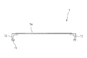
7 保持部
10 移載機構
21 流量調整バルブ
22 ヒータ
65 熱処理空間
74 サセプター
83 ガス供給管
85 ガス供給源
HL ハロゲンランプ
FL フラッシュランプ
W 半導体ウェハー
Claims (12)
- 基板に光を照射することによって該基板を加熱する熱処理装置であって、
基板を収容するチャンバーと、
前記チャンバー内にて基板を支持するサセプターと、
前記サセプターに支持された基板に光を照射する光照射部と、
前記チャンバー内に処理ガスを供給するガス供給部と、
前記ガス供給部から前記チャンバーに供給される前記処理ガスを加熱するガス加熱部と、
を備えることを特徴とする熱処理装置。 - 請求項1記載の熱処理装置において、
前記ガス加熱部は、前記チャンバー内に供給される前記処理ガスが100℃以上となるように前記処理ガスを加熱することを特徴とする熱処理装置。 - 請求項1または請求項2記載の熱処理装置において、
前記処理ガスは、窒素、酸素またはアルゴンであることを特徴とする熱処理装置。 - 請求項1から請求項3のいずれかに記載の熱処理装置において、
前記ガス供給部から前記チャンバーに供給される前記処理ガスの流量を増加する流量増加部をさらに備えることを特徴とする熱処理装置。 - 請求項1から請求項4のいずれかに記載の熱処理装置において、
前記光照射部は、前記チャンバーの一方側から基板にフラッシュ光を照射するフラッシュランプを含むことを特徴とする熱処理装置。 - 請求項5記載の熱処理装置において、
前記光照射部は、前記チャンバーの他方側から基板に光を照射するハロゲンランプをさらに含むことを特徴とする熱処理装置。 - 基板に光を照射することによって該基板を加熱する熱処理方法であって、
チャンバー内のサセプターにて基板を支持する支持工程と、
前記チャンバー内に処理ガスを供給するガス供給工程と、
前記サセプターに支持された基板に光を照射する光照射工程と、
を備え、
前記ガス供給工程は、前記チャンバーに供給する前記処理ガスを加熱するガス加熱工程を含むことを特徴とする熱処理方法。 - 請求項7記載の熱処理方法において、
前記ガス加熱工程では、前記チャンバー内に供給される前記処理ガスが100℃以上となるように前記処理ガスを加熱することを特徴する熱処理方法。 - 請求項7または請求項8記載の熱処理方法において、
前記処理ガスは、窒素、酸素またはアルゴンであることを特徴とする熱処理方法。 - 請求項7から請求項9のいずれかに記載の熱処理方法において、
前記ガス供給工程は、前記チャンバーに供給する前記処理ガスの流量を増加する流量増加工程を含むことを特徴とする熱処理方法。 - 請求項7から請求項10のいずれかに記載の熱処理方法において、
前記光照射工程では、前記チャンバーの一方側からフラッシュランプによって基板にフラッシュ光を照射することを特徴とする熱処理方法。 - 請求項11記載の熱処理方法において、
前記光照射工程では、さらに前記チャンバーの他方側からハロゲンランプによって基板に光を照射することを特徴とする熱処理方法。
Priority Applications (4)
| Application Number | Priority Date | Filing Date | Title |
|---|---|---|---|
| JP2015135256A JP2017017277A (ja) | 2015-07-06 | 2015-07-06 | 熱処理装置および熱処理方法 |
| TW105118624A TWI625791B (zh) | 2015-07-06 | 2016-06-14 | 熱處理裝置及熱處理方法 |
| US15/183,893 US9799517B2 (en) | 2015-07-06 | 2016-06-16 | Apparatus and method for light-irradiation heat treatment |
| CN201610528458.3A CN106340474A (zh) | 2015-07-06 | 2016-07-06 | 热处理装置以及热处理方法 |
Applications Claiming Priority (1)
| Application Number | Priority Date | Filing Date | Title |
|---|---|---|---|
| JP2015135256A JP2017017277A (ja) | 2015-07-06 | 2015-07-06 | 熱処理装置および熱処理方法 |
Related Child Applications (1)
| Application Number | Title | Priority Date | Filing Date |
|---|---|---|---|
| JP2019181110A Division JP2019216287A (ja) | 2019-10-01 | 2019-10-01 | 熱処理装置および熱処理方法 |
Publications (1)
| Publication Number | Publication Date |
|---|---|
| JP2017017277A true JP2017017277A (ja) | 2017-01-19 |
Family
ID=57731379
Family Applications (1)
| Application Number | Title | Priority Date | Filing Date |
|---|---|---|---|
| JP2015135256A Pending JP2017017277A (ja) | 2015-07-06 | 2015-07-06 | 熱処理装置および熱処理方法 |
Country Status (4)
| Country | Link |
|---|---|
| US (1) | US9799517B2 (ja) |
| JP (1) | JP2017017277A (ja) |
| CN (1) | CN106340474A (ja) |
| TW (1) | TWI625791B (ja) |
Cited By (4)
| Publication number | Priority date | Publication date | Assignee | Title |
|---|---|---|---|---|
| JP2018137378A (ja) * | 2017-02-23 | 2018-08-30 | 株式会社Screenホールディングス | 熱処理方法および熱処理装置 |
| JP2018186122A (ja) * | 2017-04-24 | 2018-11-22 | 株式会社Screenホールディングス | 棒状ランプおよび熱処理装置 |
| JP2021034416A (ja) * | 2019-08-16 | 2021-03-01 | 株式会社Screenホールディングス | 熱処理装置および熱処理装置の洗浄方法 |
| JP2024006279A (ja) * | 2022-07-01 | 2024-01-17 | 株式会社Screenホールディングス | 熱処理装置 |
Families Citing this family (72)
| Publication number | Priority date | Publication date | Assignee | Title |
|---|---|---|---|---|
| US9132436B2 (en) | 2012-09-21 | 2015-09-15 | Applied Materials, Inc. | Chemical control features in wafer process equipment |
| US10256079B2 (en) | 2013-02-08 | 2019-04-09 | Applied Materials, Inc. | Semiconductor processing systems having multiple plasma configurations |
| US9362130B2 (en) | 2013-03-01 | 2016-06-07 | Applied Materials, Inc. | Enhanced etching processes using remote plasma sources |
| US9309598B2 (en) | 2014-05-28 | 2016-04-12 | Applied Materials, Inc. | Oxide and metal removal |
| US9966240B2 (en) | 2014-10-14 | 2018-05-08 | Applied Materials, Inc. | Systems and methods for internal surface conditioning assessment in plasma processing equipment |
| US9355922B2 (en) | 2014-10-14 | 2016-05-31 | Applied Materials, Inc. | Systems and methods for internal surface conditioning in plasma processing equipment |
| US11637002B2 (en) | 2014-11-26 | 2023-04-25 | Applied Materials, Inc. | Methods and systems to enhance process uniformity |
| US10573496B2 (en) | 2014-12-09 | 2020-02-25 | Applied Materials, Inc. | Direct outlet toroidal plasma source |
| US20160225652A1 (en) | 2015-02-03 | 2016-08-04 | Applied Materials, Inc. | Low temperature chuck for plasma processing systems |
| US9728437B2 (en) | 2015-02-03 | 2017-08-08 | Applied Materials, Inc. | High temperature chuck for plasma processing systems |
| US9691645B2 (en) | 2015-08-06 | 2017-06-27 | Applied Materials, Inc. | Bolted wafer chuck thermal management systems and methods for wafer processing systems |
| US9741593B2 (en) | 2015-08-06 | 2017-08-22 | Applied Materials, Inc. | Thermal management systems and methods for wafer processing systems |
| US9349605B1 (en) | 2015-08-07 | 2016-05-24 | Applied Materials, Inc. | Oxide etch selectivity systems and methods |
| US10504700B2 (en) | 2015-08-27 | 2019-12-10 | Applied Materials, Inc. | Plasma etching systems and methods with secondary plasma injection |
| KR102446726B1 (ko) * | 2015-09-11 | 2022-09-26 | 삼성전자주식회사 | 투명 플레이트 및 그를 포함하는 기판 처리 장치 |
| US10504754B2 (en) | 2016-05-19 | 2019-12-10 | Applied Materials, Inc. | Systems and methods for improved semiconductor etching and component protection |
| US10522371B2 (en) | 2016-05-19 | 2019-12-31 | Applied Materials, Inc. | Systems and methods for improved semiconductor etching and component protection |
| US9865484B1 (en) | 2016-06-29 | 2018-01-09 | Applied Materials, Inc. | Selective etch using material modification and RF pulsing |
| US10629473B2 (en) | 2016-09-09 | 2020-04-21 | Applied Materials, Inc. | Footing removal for nitride spacer |
| JP6847610B2 (ja) * | 2016-09-14 | 2021-03-24 | 株式会社Screenホールディングス | 熱処理装置 |
| US10546729B2 (en) | 2016-10-04 | 2020-01-28 | Applied Materials, Inc. | Dual-channel showerhead with improved profile |
| US9934942B1 (en) | 2016-10-04 | 2018-04-03 | Applied Materials, Inc. | Chamber with flow-through source |
| US10163696B2 (en) | 2016-11-11 | 2018-12-25 | Applied Materials, Inc. | Selective cobalt removal for bottom up gapfill |
| US10026621B2 (en) | 2016-11-14 | 2018-07-17 | Applied Materials, Inc. | SiN spacer profile patterning |
| US10566206B2 (en) | 2016-12-27 | 2020-02-18 | Applied Materials, Inc. | Systems and methods for anisotropic material breakthrough |
| US10431429B2 (en) | 2017-02-03 | 2019-10-01 | Applied Materials, Inc. | Systems and methods for radial and azimuthal control of plasma uniformity |
| US10319739B2 (en) | 2017-02-08 | 2019-06-11 | Applied Materials, Inc. | Accommodating imperfectly aligned memory holes |
| JP6837871B2 (ja) * | 2017-03-09 | 2021-03-03 | 株式会社Screenホールディングス | 熱処理方法 |
| US10943834B2 (en) | 2017-03-13 | 2021-03-09 | Applied Materials, Inc. | Replacement contact process |
| US11276590B2 (en) | 2017-05-17 | 2022-03-15 | Applied Materials, Inc. | Multi-zone semiconductor substrate supports |
| US11276559B2 (en) | 2017-05-17 | 2022-03-15 | Applied Materials, Inc. | Semiconductor processing chamber for multiple precursor flow |
| JP7176860B6 (ja) | 2017-05-17 | 2022-12-16 | アプライド マテリアルズ インコーポレイテッド | 前駆体の流れを改善する半導体処理チャンバ |
| US10497579B2 (en) | 2017-05-31 | 2019-12-03 | Applied Materials, Inc. | Water-free etching methods |
| US10920320B2 (en) | 2017-06-16 | 2021-02-16 | Applied Materials, Inc. | Plasma health determination in semiconductor substrate processing reactors |
| US10541246B2 (en) | 2017-06-26 | 2020-01-21 | Applied Materials, Inc. | 3D flash memory cells which discourage cross-cell electrical tunneling |
| US10727080B2 (en) | 2017-07-07 | 2020-07-28 | Applied Materials, Inc. | Tantalum-containing material removal |
| US10541184B2 (en) | 2017-07-11 | 2020-01-21 | Applied Materials, Inc. | Optical emission spectroscopic techniques for monitoring etching |
| US10043674B1 (en) | 2017-08-04 | 2018-08-07 | Applied Materials, Inc. | Germanium etching systems and methods |
| US10297458B2 (en) | 2017-08-07 | 2019-05-21 | Applied Materials, Inc. | Process window widening using coated parts in plasma etch processes |
| US10903054B2 (en) | 2017-12-19 | 2021-01-26 | Applied Materials, Inc. | Multi-zone gas distribution systems and methods |
| US11328909B2 (en) | 2017-12-22 | 2022-05-10 | Applied Materials, Inc. | Chamber conditioning and removal processes |
| US10854426B2 (en) | 2018-01-08 | 2020-12-01 | Applied Materials, Inc. | Metal recess for semiconductor structures |
| JP6960344B2 (ja) * | 2018-01-26 | 2021-11-05 | 株式会社Screenホールディングス | 熱処理方法および熱処理装置 |
| US10679870B2 (en) | 2018-02-15 | 2020-06-09 | Applied Materials, Inc. | Semiconductor processing chamber multistage mixing apparatus |
| US10964512B2 (en) | 2018-02-15 | 2021-03-30 | Applied Materials, Inc. | Semiconductor processing chamber multistage mixing apparatus and methods |
| JP7042115B2 (ja) | 2018-02-28 | 2022-03-25 | 株式会社Screenホールディングス | 熱処理装置および熱処理方法 |
| TWI766433B (zh) | 2018-02-28 | 2022-06-01 | 美商應用材料股份有限公司 | 形成氣隙的系統及方法 |
| US10593560B2 (en) | 2018-03-01 | 2020-03-17 | Applied Materials, Inc. | Magnetic induction plasma source for semiconductor processes and equipment |
| US10319600B1 (en) | 2018-03-12 | 2019-06-11 | Applied Materials, Inc. | Thermal silicon etch |
| US10497573B2 (en) | 2018-03-13 | 2019-12-03 | Applied Materials, Inc. | Selective atomic layer etching of semiconductor materials |
| US10573527B2 (en) | 2018-04-06 | 2020-02-25 | Applied Materials, Inc. | Gas-phase selective etching systems and methods |
| US10490406B2 (en) | 2018-04-10 | 2019-11-26 | Appled Materials, Inc. | Systems and methods for material breakthrough |
| US10699879B2 (en) | 2018-04-17 | 2020-06-30 | Applied Materials, Inc. | Two piece electrode assembly with gap for plasma control |
| JP7088732B2 (ja) * | 2018-04-27 | 2022-06-21 | 株式会社堀場エステック | 基板処理装置及び基板処理装置用プログラム |
| US10886137B2 (en) | 2018-04-30 | 2021-01-05 | Applied Materials, Inc. | Selective nitride removal |
| JP7041594B2 (ja) * | 2018-06-20 | 2022-03-24 | 株式会社Screenホールディングス | 熱処理装置 |
| JP6963536B2 (ja) * | 2018-06-20 | 2021-11-10 | 株式会社Screenホールディングス | 熱処理装置および熱処理装置の雰囲気置換方法 |
| US10514167B1 (en) * | 2018-06-29 | 2019-12-24 | Taiwan Semiconductor Manufacturing Co., Ltd. | Method and apparatus for controlling exhaust pressure for an extreme ultraviolet generation chamber |
| US10872778B2 (en) | 2018-07-06 | 2020-12-22 | Applied Materials, Inc. | Systems and methods utilizing solid-phase etchants |
| US10755941B2 (en) | 2018-07-06 | 2020-08-25 | Applied Materials, Inc. | Self-limiting selective etching systems and methods |
| US10672642B2 (en) | 2018-07-24 | 2020-06-02 | Applied Materials, Inc. | Systems and methods for pedestal configuration |
| US10892198B2 (en) | 2018-09-14 | 2021-01-12 | Applied Materials, Inc. | Systems and methods for improved performance in semiconductor processing |
| US11049755B2 (en) | 2018-09-14 | 2021-06-29 | Applied Materials, Inc. | Semiconductor substrate supports with embedded RF shield |
| US11062887B2 (en) | 2018-09-17 | 2021-07-13 | Applied Materials, Inc. | High temperature RF heater pedestals |
| US11417534B2 (en) | 2018-09-21 | 2022-08-16 | Applied Materials, Inc. | Selective material removal |
| US11682560B2 (en) | 2018-10-11 | 2023-06-20 | Applied Materials, Inc. | Systems and methods for hafnium-containing film removal |
| US11121002B2 (en) | 2018-10-24 | 2021-09-14 | Applied Materials, Inc. | Systems and methods for etching metals and metal derivatives |
| US11437242B2 (en) | 2018-11-27 | 2022-09-06 | Applied Materials, Inc. | Selective removal of silicon-containing materials |
| US11721527B2 (en) | 2019-01-07 | 2023-08-08 | Applied Materials, Inc. | Processing chamber mixing systems |
| US10920319B2 (en) | 2019-01-11 | 2021-02-16 | Applied Materials, Inc. | Ceramic showerheads with conductive electrodes |
| JP7294858B2 (ja) * | 2019-04-09 | 2023-06-20 | 株式会社Screenホールディングス | 熱処理方法および熱処理装置 |
| CN114823331B (zh) * | 2022-04-22 | 2023-03-03 | 江苏晟驰微电子有限公司 | 一种用于三极管器件制造的氮氢退火设备及其工艺 |
Citations (6)
| Publication number | Priority date | Publication date | Assignee | Title |
|---|---|---|---|---|
| JPH0324720A (ja) * | 1989-06-22 | 1991-02-01 | Toshiba Corp | ウェハ処理方法及び処理装置 |
| JPH1154491A (ja) * | 1997-08-04 | 1999-02-26 | Kokusai Electric Co Ltd | ガス供給方法 |
| JP2000012478A (ja) * | 1998-06-18 | 2000-01-14 | Dainippon Screen Mfg Co Ltd | 基板熱処理装置 |
| JP2000058469A (ja) * | 1998-08-07 | 2000-02-25 | Dainippon Screen Mfg Co Ltd | 基板熱処理装置 |
| JP2007281225A (ja) * | 2006-04-07 | 2007-10-25 | Tokyo Electron Ltd | 処理装置及び処理方法 |
| JP2013207033A (ja) * | 2012-03-28 | 2013-10-07 | Dainippon Screen Mfg Co Ltd | 熱処理装置および熱処理方法 |
Family Cites Families (7)
| Publication number | Priority date | Publication date | Assignee | Title |
|---|---|---|---|---|
| JPS60258928A (ja) | 1984-02-28 | 1985-12-20 | タマラツク・サイエンテイフイツク・カンパニ−・インコ−ポレ−テツド | 半導体ウエ−ハの加熱装置および方法 |
| US4649261A (en) | 1984-02-28 | 1987-03-10 | Tamarack Scientific Co., Inc. | Apparatus for heating semiconductor wafers in order to achieve annealing, silicide formation, reflow of glass passivation layers, etc. |
| DE69420474T2 (de) * | 1993-06-30 | 2000-05-18 | Applied Materials Inc | Verfahren zum Spülen und Auspumpen einer Vakuumkammer bis Ultra-Hoch-Vakuum |
| US6331212B1 (en) | 2000-04-17 | 2001-12-18 | Avansys, Llc | Methods and apparatus for thermally processing wafers |
| US6849831B2 (en) | 2002-03-29 | 2005-02-01 | Mattson Technology, Inc. | Pulsed processing semiconductor heating methods using combinations of heating sources |
| TWI566300B (zh) * | 2011-03-23 | 2017-01-11 | 斯克林集團公司 | 熱處理方法及熱處理裝置 |
| JP6560550B2 (ja) * | 2015-07-06 | 2019-08-14 | 株式会社Screenホールディングス | 熱処理方法および熱処理装置 |
-
2015
- 2015-07-06 JP JP2015135256A patent/JP2017017277A/ja active Pending
-
2016
- 2016-06-14 TW TW105118624A patent/TWI625791B/zh active
- 2016-06-16 US US15/183,893 patent/US9799517B2/en active Active
- 2016-07-06 CN CN201610528458.3A patent/CN106340474A/zh active Pending
Patent Citations (6)
| Publication number | Priority date | Publication date | Assignee | Title |
|---|---|---|---|---|
| JPH0324720A (ja) * | 1989-06-22 | 1991-02-01 | Toshiba Corp | ウェハ処理方法及び処理装置 |
| JPH1154491A (ja) * | 1997-08-04 | 1999-02-26 | Kokusai Electric Co Ltd | ガス供給方法 |
| JP2000012478A (ja) * | 1998-06-18 | 2000-01-14 | Dainippon Screen Mfg Co Ltd | 基板熱処理装置 |
| JP2000058469A (ja) * | 1998-08-07 | 2000-02-25 | Dainippon Screen Mfg Co Ltd | 基板熱処理装置 |
| JP2007281225A (ja) * | 2006-04-07 | 2007-10-25 | Tokyo Electron Ltd | 処理装置及び処理方法 |
| JP2013207033A (ja) * | 2012-03-28 | 2013-10-07 | Dainippon Screen Mfg Co Ltd | 熱処理装置および熱処理方法 |
Cited By (7)
| Publication number | Priority date | Publication date | Assignee | Title |
|---|---|---|---|---|
| JP2018137378A (ja) * | 2017-02-23 | 2018-08-30 | 株式会社Screenホールディングス | 熱処理方法および熱処理装置 |
| JP2018186122A (ja) * | 2017-04-24 | 2018-11-22 | 株式会社Screenホールディングス | 棒状ランプおよび熱処理装置 |
| US11189506B2 (en) | 2017-04-24 | 2021-11-30 | SCREEN Holdings Co., Ltd. | Rod-shaped lamp and heat treatment apparatus |
| JP2021034416A (ja) * | 2019-08-16 | 2021-03-01 | 株式会社Screenホールディングス | 熱処理装置および熱処理装置の洗浄方法 |
| JP7304768B2 (ja) | 2019-08-16 | 2023-07-07 | 株式会社Screenホールディングス | 熱処理装置および熱処理装置の洗浄方法 |
| US12160936B2 (en) | 2019-08-16 | 2024-12-03 | SCREEN Holdings Co., Ltd. | Heat treatment apparatus of light irradiation type and method for cleaning heat treatment apparatus |
| JP2024006279A (ja) * | 2022-07-01 | 2024-01-17 | 株式会社Screenホールディングス | 熱処理装置 |
Also Published As
| Publication number | Publication date |
|---|---|
| CN106340474A (zh) | 2017-01-18 |
| TWI625791B (zh) | 2018-06-01 |
| US9799517B2 (en) | 2017-10-24 |
| TW201709336A (zh) | 2017-03-01 |
| US20170011922A1 (en) | 2017-01-12 |
Similar Documents
| Publication | Publication Date | Title |
|---|---|---|
| JP6560550B2 (ja) | 熱処理方法および熱処理装置 | |
| US9799517B2 (en) | Apparatus and method for light-irradiation heat treatment | |
| JP5955604B2 (ja) | 熱処理装置および熱処理方法 | |
| JP6587955B2 (ja) | 熱処理装置 | |
| KR102033843B1 (ko) | 열처리 방법 및 열처리 장치 | |
| JP7319894B2 (ja) | 熱処理装置 | |
| KR102126119B1 (ko) | 열처리 방법 | |
| JP6622617B2 (ja) | 熱処理装置 | |
| JP2016225429A (ja) | 熱処理装置 | |
| JP6770915B2 (ja) | 熱処理装置 | |
| JP2018152405A (ja) | 熱処理方法および熱処理装置 | |
| JP6647892B2 (ja) | 熱処理用サセプタおよび熱処理装置 | |
| KR102407656B1 (ko) | 열처리 방법 및 열처리 장치 | |
| JP2019021828A (ja) | 熱処理装置 | |
| JP5964630B2 (ja) | 熱処理装置 | |
| JP2018133424A (ja) | 熱処理装置 | |
| JP6438331B2 (ja) | 熱処理装置 | |
| JP6637321B2 (ja) | 熱処理用サセプタおよび熱処理装置 | |
| JP6469479B2 (ja) | 基板温度調整方法 | |
| JP6438326B2 (ja) | 熱処理装置 | |
| JP2015018941A (ja) | 熱処理装置 | |
| JP2019057613A (ja) | 熱処理装置 | |
| JP2018098315A (ja) | 熱処理方法および熱処理装置 | |
| JP7300365B2 (ja) | 熱処理装置 | |
| WO2019181046A1 (ja) | 熱処理装置および熱処理方法 |
Legal Events
| Date | Code | Title | Description |
|---|---|---|---|
| A621 | Written request for application examination |
Free format text: JAPANESE INTERMEDIATE CODE: A621 Effective date: 20180626 |
|
| A131 | Notification of reasons for refusal |
Free format text: JAPANESE INTERMEDIATE CODE: A131 Effective date: 20190219 |
|
| A977 | Report on retrieval |
Free format text: JAPANESE INTERMEDIATE CODE: A971007 Effective date: 20190221 |
|
| A521 | Request for written amendment filed |
Free format text: JAPANESE INTERMEDIATE CODE: A523 Effective date: 20190415 |
|
| A02 | Decision of refusal |
Free format text: JAPANESE INTERMEDIATE CODE: A02 Effective date: 20190702 |