JP2017045009A - 光変調器 - Google Patents
光変調器 Download PDFInfo
- Publication number
- JP2017045009A JP2017045009A JP2015169750A JP2015169750A JP2017045009A JP 2017045009 A JP2017045009 A JP 2017045009A JP 2015169750 A JP2015169750 A JP 2015169750A JP 2015169750 A JP2015169750 A JP 2015169750A JP 2017045009 A JP2017045009 A JP 2017045009A
- Authority
- JP
- Japan
- Prior art keywords
- region
- type impurity
- impurity region
- slab
- silicon
- Prior art date
- Legal status (The legal status is an assumption and is not a legal conclusion. Google has not performed a legal analysis and makes no representation as to the accuracy of the status listed.)
- Pending
Links
Images



Landscapes
- Optical Modulation, Optical Deflection, Nonlinear Optics, Optical Demodulation, Optical Logic Elements (AREA)
Abstract
Description
102、202 下部クラッド層
103、203 リブ導波路
104、204 上部クラッド層
111、211 p型不純物領域
112、212 n型不純物領域
113、213 高濃度p型不純物領域
114、214 高濃度n型不純物領域
116、117、216、217 金属電極
120、220 スラブ領域
115 不純物が打ち込まれていない領域
215 オーバーラップ領域
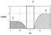
10 不純物が打ち込まれていない領域の不純物濃度
11、21 p型不純物濃度
12、22 n型不純物濃度
23 オーバーラップ領域の不純物濃度
321 p型イオン
322 n型イオン
331、332 遮蔽体
Claims (3)
- シリコン基板と、
前記シリコン基板上に形成された下部クラッド層と、
前記下部クラッド層上に形成された凸部および前記凸部の両側の第1および第2のスラブ領域とからなる、リブ導波路であって、前記凸部はp型不純物が打ち込まれたp型不純物領域、p型不純物およびn型不純物が打ち込まれたオーバーラップ領域、ならびにn型不純物が打ち込まれたn型不純物領域を含み、前記凸部のp型不純物領域側の前記第1のスラブ領域はp型不純物領域を含み、前記凸部のn型不純物領域側の前記第2のスラブ領域はn型不純物領域を含む、リブ導波路と、
前記リブ導波路上に形成された上部クラッド層と、
前記第1のスラブ領域および前記第2のスラブ領域にそれぞれ接合された電極と、
を備えたことを特徴する光変調器。 - 前記第1のスラブ領域は、高濃度p型不純物領域を含み、
前記第2のスラブ領域は、高濃度n型不純物領域を含み、
前記電極は、前記第1のスラブ領域の高濃度p型不純物領域および前記第2のスラブ領域の高濃度n型不純物領域とそれぞれオーミック接続を形成していることを特徴とする請求項1記載の光変調器。 - 前記下部クラッド層は、シリコン酸化膜であることを特徴とする請求項1又は2に記載の光変調器。
Priority Applications (1)
| Application Number | Priority Date | Filing Date | Title |
|---|---|---|---|
| JP2015169750A JP2017045009A (ja) | 2015-08-28 | 2015-08-28 | 光変調器 |
Applications Claiming Priority (1)
| Application Number | Priority Date | Filing Date | Title |
|---|---|---|---|
| JP2015169750A JP2017045009A (ja) | 2015-08-28 | 2015-08-28 | 光変調器 |
Publications (1)
| Publication Number | Publication Date |
|---|---|
| JP2017045009A true JP2017045009A (ja) | 2017-03-02 |
Family
ID=58210224
Family Applications (1)
| Application Number | Title | Priority Date | Filing Date |
|---|---|---|---|
| JP2015169750A Pending JP2017045009A (ja) | 2015-08-28 | 2015-08-28 | 光変調器 |
Country Status (1)
| Country | Link |
|---|---|
| JP (1) | JP2017045009A (ja) |
Cited By (1)
| Publication number | Priority date | Publication date | Assignee | Title |
|---|---|---|---|---|
| JP2023145961A (ja) * | 2022-03-29 | 2023-10-12 | 日本電気株式会社 | 光導波路モジュール及び光導波路モジュールの製造方法 |
Citations (1)
| Publication number | Priority date | Publication date | Assignee | Title |
|---|---|---|---|---|
| US20140341497A1 (en) * | 2013-05-14 | 2014-11-20 | Yang Liu | Ultra-responsive phase shifters for depletion mode silicon modulators |
-
2015
- 2015-08-28 JP JP2015169750A patent/JP2017045009A/ja active Pending
Patent Citations (1)
| Publication number | Priority date | Publication date | Assignee | Title |
|---|---|---|---|---|
| US20140341497A1 (en) * | 2013-05-14 | 2014-11-20 | Yang Liu | Ultra-responsive phase shifters for depletion mode silicon modulators |
Cited By (2)
| Publication number | Priority date | Publication date | Assignee | Title |
|---|---|---|---|---|
| JP2023145961A (ja) * | 2022-03-29 | 2023-10-12 | 日本電気株式会社 | 光導波路モジュール及び光導波路モジュールの製造方法 |
| JP7852337B2 (ja) | 2022-03-29 | 2026-04-28 | 日本電気株式会社 | 光導波路モジュール、光送信モジュール及び光導波路モジュールの製造方法 |
Similar Documents
| Publication | Publication Date | Title |
|---|---|---|
| US10133098B2 (en) | MOS capacitor optical modulator with transparent conductive and low-refractive-index gate | |
| CN111051969B (zh) | 相位调制器及其制作方法、硅基电光调制器 | |
| GB2593354A (en) | PN-junction phase modulator in a large silicon waveguide platform | |
| US9323079B1 (en) | Optical device having electro-optic silicon modulator on large core fin waveguide and method to make the same | |
| US9618776B2 (en) | Electro-absorption optical modulation device and method of fabricating the same | |
| KR102449211B1 (ko) | 전계 효과 트랜지스터를 포함하는 반도체 소자 | |
| AU2014375262B2 (en) | Structure for optical waveguide and contact wire intersection | |
| US20170102564A1 (en) | Semiconductor optical waveguide, semiconductor optical mudulator, and semiconductor optical modulation system | |
| CN105487263A (zh) | 硅基脊型波导调制器及其制造方法 | |
| US20210320200A1 (en) | Termination for trench field plate power mosfet | |
| US20180138288A1 (en) | Silicon carbide semiconductor element and method of manufacturing silicon carbide semiconductor | |
| WO2014181665A1 (ja) | 半導体エネルギー線検出素子及び半導体エネルギー線検出素子の製造方法 | |
| CN102681370A (zh) | 光刻套刻方法和提高ldmos器件击穿稳定性的方法 | |
| JP2017045009A (ja) | 光変調器 | |
| KR102268815B1 (ko) | 광 전자 소자 및 이의 제조 방법 | |
| CN105378548A (zh) | 一种掺杂结构及其制作方法、电光调制器 | |
| CN104979283A (zh) | Ti-igbt的制作方法 | |
| KR20140033078A (ko) | 바이폴라 펀치 쓰루 반도체 디바이스 및 그러한 반도체 디바이스의 제조 방법 | |
| US20160005843A1 (en) | Semiconductor device and manufacturing method thereof | |
| JP5201169B2 (ja) | 誘電体分離型半導体装置の製造方法 | |
| JP2016181558A (ja) | 半導体受光素子 | |
| TWI525813B (zh) | 電晶體裝置及其製造方法 | |
| JP6351863B2 (ja) | 半導体装置 | |
| JPH02142184A (ja) | 半導体装置及びその製造方法 | |
| JP2015185656A (ja) | 半導体装置 |
Legal Events
| Date | Code | Title | Description |
|---|---|---|---|
| A621 | Written request for application examination |
Free format text: JAPANESE INTERMEDIATE CODE: A621 Effective date: 20170223 |
|
| A977 | Report on retrieval |
Free format text: JAPANESE INTERMEDIATE CODE: A971007 Effective date: 20180124 |
|
| A131 | Notification of reasons for refusal |
Free format text: JAPANESE INTERMEDIATE CODE: A131 Effective date: 20180206 |
|
| A521 | Request for written amendment filed |
Free format text: JAPANESE INTERMEDIATE CODE: A523 Effective date: 20180409 |
|
| A02 | Decision of refusal |
Free format text: JAPANESE INTERMEDIATE CODE: A02 Effective date: 20180814 |