JP2017103014A - Method of manufacturing electrode plate - Google Patents
Method of manufacturing electrode plate Download PDFInfo
- Publication number
- JP2017103014A JP2017103014A JP2015233429A JP2015233429A JP2017103014A JP 2017103014 A JP2017103014 A JP 2017103014A JP 2015233429 A JP2015233429 A JP 2015233429A JP 2015233429 A JP2015233429 A JP 2015233429A JP 2017103014 A JP2017103014 A JP 2017103014A
- Authority
- JP
- Japan
- Prior art keywords
- roll
- active material
- material layer
- gap
- electrode plate
- Prior art date
- Legal status (The legal status is an assumption and is not a legal conclusion. Google has not performed a legal analysis and makes no representation as to the accuracy of the status listed.)
- Granted
Links
Images




Classifications
-
- H—ELECTRICITY
- H01—ELECTRIC ELEMENTS
- H01M—PROCESSES OR MEANS, e.g. BATTERIES, FOR THE DIRECT CONVERSION OF CHEMICAL ENERGY INTO ELECTRICAL ENERGY
- H01M4/00—Electrodes
- H01M4/02—Electrodes composed of, or comprising, active material
- H01M4/04—Processes of manufacture in general
- H01M4/043—Processes of manufacture in general involving compressing or compaction
- H01M4/0435—Rolling or calendering
-
- H—ELECTRICITY
- H01—ELECTRIC ELEMENTS
- H01M—PROCESSES OR MEANS, e.g. BATTERIES, FOR THE DIRECT CONVERSION OF CHEMICAL ENERGY INTO ELECTRICAL ENERGY
- H01M4/00—Electrodes
- H01M4/02—Electrodes composed of, or comprising, active material
- H01M2004/026—Electrodes composed of, or comprising, active material characterised by the polarity
- H01M2004/028—Positive electrodes
-
- Y—GENERAL TAGGING OF NEW TECHNOLOGICAL DEVELOPMENTS; GENERAL TAGGING OF CROSS-SECTIONAL TECHNOLOGIES SPANNING OVER SEVERAL SECTIONS OF THE IPC; TECHNICAL SUBJECTS COVERED BY FORMER USPC CROSS-REFERENCE ART COLLECTIONS [XRACs] AND DIGESTS
- Y02—TECHNOLOGIES OR APPLICATIONS FOR MITIGATION OR ADAPTATION AGAINST CLIMATE CHANGE
- Y02E—REDUCTION OF GREENHOUSE GAS [GHG] EMISSIONS, RELATED TO ENERGY GENERATION, TRANSMISSION OR DISTRIBUTION
- Y02E60/00—Enabling technologies; Technologies with a potential or indirect contribution to GHG emissions mitigation
- Y02E60/10—Energy storage using batteries
Landscapes
- Engineering & Computer Science (AREA)
- Manufacturing & Machinery (AREA)
- Chemical & Material Sciences (AREA)
- Chemical Kinetics & Catalysis (AREA)
- Electrochemistry (AREA)
- General Chemical & Material Sciences (AREA)
- Application Of Or Painting With Fluid Materials (AREA)
- Battery Electrode And Active Subsutance (AREA)
Abstract
【課題】均一な厚みの活物質層を有する電極板の製造方法を提供すること。【解決手段】本発明に係る電極板の製造方法は,第1の位置で対向する第1のロールと第2のロールとの隙間の大きさを第1の設定値に設定し,第1の位置に電極材料を通過させて,第2のロール上に活物質層を形成する成膜工程を有する。また,第2の位置で対向する第2のロールと第3のロールとの隙間の大きさを第2の設定値に設定し,第2の位置に,第2のロール上の活物質層を集電箔とともに通過させて,活物質層を集電箔上に転写する転写工程とを有する。さらに,成膜工程を,第2のロールと第3のロールとの隙間の大きさを第2の設定値よりも大きな離間状態として開始する。そして,第2のロール上の活物質層の先端が第2の位置に到達した後,第2のロールと第3のロールとの隙間の大きさを第2の設定値とする隙間調整を行う。【選択図】図6An electrode plate having an active material layer having a uniform thickness is provided. A method of manufacturing an electrode plate according to the present invention sets a size of a gap between a first roll and a second roll facing each other at a first position to a first set value, A film forming step of forming an active material layer on the second roll by passing the electrode material through the position; Further, the size of the gap between the second roll and the third roll facing each other at the second position is set to the second set value, and the active material layer on the second roll is placed at the second position. And a transfer step of transferring the active material layer onto the current collector foil through the current collector foil. Further, the film forming process is started with the size of the gap between the second roll and the third roll being in a separated state larger than the second set value. And after the front-end | tip of the active material layer on a 2nd roll arrives at a 2nd position, the clearance gap adjustment which makes the magnitude | size of the clearance gap between a 2nd roll and a 3rd roll a 2nd setting value is performed . [Selection] Figure 6
Description
本発明は,電極板の製造方法に関する。より詳細には,電極材料をロール対の間に通過させて加圧することにより活物質層となし,その活物質層を集電箔の表面に転写して電極板を製造する電極板の製造方法に関するものである。 The present invention relates to a method for manufacturing an electrode plate. More specifically, an electrode plate is manufactured by passing an electrode material between roll pairs and applying pressure to form an active material layer, and transferring the active material layer to the surface of the current collector foil. It is about.
リチウムイオン二次電池などの電池は,正負の電極板と電解液とをケース内部に収容してなるものである。正負の電極板は,集電箔と活物質層とを有するものである。活物質層には,充放電に寄与する活物質,活物質を集電箔上に結着させて活物質層を形成するための結着材などの電極材料が含まれている。そして,このような電極板の製造方法に係る先行技術として,例えば,特許文献1に記載のものが挙げられる。
A battery such as a lithium ion secondary battery is one in which positive and negative electrode plates and an electrolytic solution are accommodated in a case. The positive and negative electrode plates have a current collector foil and an active material layer. The active material layer includes an electrode material such as an active material that contributes to charging and discharging, and a binder for binding the active material on the current collector foil to form an active material layer. And as a prior art which concerns on the manufacturing method of such an electrode plate, the thing of
特許文献1の図6に係る装置では,まず,活物質や結着材等よりなる電極材料を,第1ロールと第2ロールとの対向位置に供給し,その対向位置の隙間に通過させることにより成形して活物質層としている。また,成形され,第2ロール上に付着している活物質層を,第2ロールと第3ロールとの対向位置の隙間に集電箔とともに通過させることにより,集電箔上に転写している。これにより,集電箔上に活物質層を有する電極板を製造している。
In the apparatus according to FIG. 6 of
しかしながら,上記のような従来技術では,搬送方向における長さの長い電極板を,その搬送方向について均一な厚みの活物質層を形成しつつ製造することが困難であった。すなわち,電極材料は,第1ロールと第2ロールとの対向位置において加圧されることにより活物質層とされる。また,第2ロール上の活物質層は,第2ロールと第3ロールとの対向位置において集電箔とともに厚み方向に加圧されることにより,集電箔上に転写される。 However, in the conventional technology as described above, it is difficult to manufacture an electrode plate having a long length in the transport direction while forming an active material layer having a uniform thickness in the transport direction. That is, the electrode material is pressed into an active material layer at a position where the first roll and the second roll face each other. Further, the active material layer on the second roll is transferred onto the current collector foil by being pressed together with the current collector foil in the thickness direction at a position opposite to the second roll and the third roll.
そして,第1ロールと第2ロールとの対向位置に電極材料が通過するとき,第1ロールおよび第2ロールはそれぞれ,電極材料を加圧する反力を,互いに遠ざかる向きに受ける。また,第2ロールと第3ロールとの対向位置に活物質層と集電箔とが通過するとき,第2ロールおよび第3ロールはそれぞれ,活物質層および集電箔を加圧する反力を,互いに遠ざかる向きに受ける。 And when an electrode material passes the opposing position of a 1st roll and a 2nd roll, a 1st roll and a 2nd roll each receive the reaction force which pressurizes an electrode material in the direction away from each other. In addition, when the active material layer and the current collector foil pass through the opposing positions of the second roll and the third roll, the second roll and the third roll have a reaction force that pressurizes the active material layer and the current collector foil, respectively. , Receive in directions away from each other.
つまり,電極板を製造中において,第1ロールと第2ロールとの対向位置の隙間,第2ロールと第3ロールとの対向位置の隙間は変化することがある。このため,その隙間を通過することにより製造される電極板の活物質層の厚みについても,隙間の変化に伴って変化してしまうからである。 That is, during manufacture of the electrode plate, the gap at the opposing position between the first roll and the second roll and the gap at the opposing position between the second roll and the third roll may change. For this reason, it is because the thickness of the active material layer of the electrode plate manufactured by passing through the gap also changes as the gap changes.
本発明は,前記した従来の技術が有する問題点の解決を目的としてなされたものである。すなわちその課題とするところは,均一な厚みの活物質層を有する電極板の製造方法を提供することである。 The present invention has been made for the purpose of solving the problems of the prior art described above. That is, the problem is to provide a method for producing an electrode plate having an active material layer having a uniform thickness.
この課題の解決を目的としてなされた本発明の電極板の製造方法は,外周面の一箇所同士が互いに対向するとともに,外周面同士が対向する第1の位置における外周面の移動方向がともに同じとなる向きに回転する第1のロールおよび第2のロールと,第2のロールと外周面の一箇所同士が第1の位置以外の第2の位置にて互いに対向するとともに,第2の位置における外周面の移動方向が第2のロールの外周面の移動方向と同じとなる向きに回転する第3のロールとを有する電極板製造装置を用い,第1のロールと第2のロールとの隙間の大きさを第1の設定値に設定した第1の位置に,活物質および結着材を少なくとも含む電極材料を通過させて,第2のロール上に活物質層を形成する成膜工程と,第2のロールと第3のロールとの隙間の大きさを第2の設定値に設定した第2の位置に,第2のロール上の活物質層を第3のロールに巻き回されている集電箔とともに通過させて,活物質層を集電箔上に転写して電極板となす転写工程とを有する電極板の製造方法であって,成膜工程を,第2のロールと第3のロールとの隙間の大きさを第2の設定値よりも大きな離間状態として開始し,開始された成膜工程により第2のロール上に形成された活物質層の先端が第2の位置に到達した後,活物質層が第2の位置に存在する状態で,第2のロールおよび第3のロールの少なくとも一方を他方に向けて移動させ,第2のロールと第3のロールとの隙間の大きさを第2の設定値とする隙間調整を行うことを特徴とする電極板の製造方法である。 The electrode plate manufacturing method of the present invention, which has been made for the purpose of solving this problem, is such that one part of the outer peripheral surface faces each other and the movement direction of the outer peripheral surface at the first position where the outer peripheral surfaces face each other is the same. The first roll and the second roll that rotate in the direction to be, and the second roll and one outer peripheral surface face each other at a second position other than the first position, and the second position Using an electrode plate manufacturing apparatus having a third roll rotating in a direction in which the movement direction of the outer peripheral surface of the second roll is the same as the movement direction of the outer peripheral surface of the second roll, A film forming step of forming an active material layer on the second roll by passing an electrode material containing at least an active material and a binder to a first position where the size of the gap is set to a first set value. And the gap between the second roll and the third roll Pass the active material layer on the second roll with the current collector foil wound around the third roll to the second position where the size is set to the second set value, and collect the active material layer. A method of manufacturing an electrode plate having a transfer step of transferring onto an electric foil to form an electrode plate, wherein a film forming step is performed, and a size of a gap between the second roll and the third roll is set to a second setting Starting from a separated state larger than the value, and after the leading edge of the active material layer formed on the second roll by the started film formation process reaches the second position, the active material layer is moved to the second position. In the existing state, at least one of the second roll and the third roll is moved toward the other, and the gap adjustment between the second roll and the third roll is set to the second set value. It is the manufacturing method of the electrode plate characterized by performing.
本発明に係る電極板の製造方法では,隙間調整により,第1の位置と第2の位置とに加圧対象が存在する状態で第2の位置の隙間の大きさを調整することができる。このため,本形態では,第2のロールの加圧に伴う移動の影響を受けることなく,第2の位置の隙間を調整することができる。よって,第2の位置の隙間の大きさを一定とし,均一な厚みの活物質層を有する電極板を製造することができる。 In the method of manufacturing the electrode plate according to the present invention, the size of the gap at the second position can be adjusted by adjusting the gap while the object to be pressed exists at the first position and the second position. For this reason, in this embodiment, the gap at the second position can be adjusted without being affected by the movement accompanying the pressurization of the second roll. Therefore, it is possible to manufacture an electrode plate having an active material layer with a uniform thickness while keeping the size of the gap at the second position constant.
本発明によれば,均一な厚みの活物質層を有する電極板の製造方法が提供されている。 According to the present invention, a method for manufacturing an electrode plate having an active material layer having a uniform thickness is provided.
以下,本発明を具体化した最良の形態について,図面を参照しつつ詳細に説明する。 DESCRIPTION OF THE PREFERRED EMBODIMENTS Hereinafter, the best mode for embodying the present invention will be described in detail with reference to the drawings.
まず,図1により,本形態において製造される電極板100について説明する。電極板100は,図1の断面図に示すように,集電箔110と,活物質層120とを有している。電極板100は,図1において左右方向に長いものである。
First, the
本形態の電極板100において,活物質層120は,集電箔110の第1面111のみに形成されている。電極板100は,例えば,リチウムイオン二次電池などの二次電池を構成するための正極または負極として用いられるものである。電極板100は,正極または負極として二次電池の製造に用いられる際には,適宜,必要なサイズに切り出される。
In the
集電箔110としては,例えば,金属箔を用いることができる。また,活物質層120は少なくとも,活物質121および結着材122を含むものである。活物質121は,電池における充放電に寄与するものである。また,結着材122は,活物質層120を構成する材料を互いに結着させて活物質層120を形成するとともに,その活物質層120を集電箔110の第1面111に結着させるためのものである。
For example, a metal foil can be used as the
具体的には,電極板100がリチウムイオン二次電池の正極である場合,例えば,集電箔110としてアルミニウム箔を,活物質121としてLiNi0.5Mn1.5O4を,結着材122としてポリフッ化ビニリデン(PVDF)を用いることができる。あるいは,電極板100がリチウムイオン二次電池の負極である場合,例えば,集電箔110として銅箔を,活物質121として炭素材料を,結着材122としてスチレンブタジエンゴム(SBR)を用いることができる。なお,活物質層120には,適宜,活物質層120内の導電性を高めるための導電材など,活物質121および結着材122以外の材料がさらに含まれていても良い。
Specifically, when the
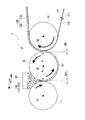
次に,本形態において電極板100の製造に用いる電極板製造装置について説明する。図2に,本形態の電極板製造装置1の概略構成図を示している。電極板製造装置1は,図2に示すように,第1ロール10,第2ロール20,第3ロール30を有している。図2において,上下方向が鉛直方向であり,重力は下向きに作用している。
Next, an electrode plate manufacturing apparatus used for manufacturing the
本形態の電極板製造装置1において,第1ロール10,第2ロール20,第3ロール30はいずれも,軸方向を水平にした状態で配置されている。第1ロール10,第2ロール20,第3ロール30は,例えば,金属などの材質のものである。また,第1ロール10および第2ロール20は,それぞれの外周面11,21が第1対向位置Aにおいて互いに対向した状態で,平行に配置されている。また,第3ロール30は,第2ロール20と外周面21,31が第2対向位置Bにおいて互いに対向した状態で,第2ロール20と平行に配置されている。
In the electrode
第1ロール10および第2ロール20は,軸間距離が一定の距離となるように保持されている。そして,第1対向位置Aにおける第1ロール10の外周面11と第2ロール20の外周面21との間には,隙間が設けられている。この第1対向位置Aにおける隙間の大きさを,GAにより示している。なお,図2に示しているGAは,第1対向位置Aにおける隙間の大きさの設定値である。
The
また,第3ロール30は,第2ロール20との軸間距離が一定の距離となるように保持されている。そして,第2対向位置Bにおける第2ロール20の外周面21と第3ロール30の外周面31との間には,隙間が設けられている。この第2対向位置Bにおける隙間の大きさを,GB1により示している。なお,図2に示しているGB1についても,第2対向位置Bにおける隙間の大きさの設定値である。
The
また,第1ロール10,第2ロール20,第3ロール30は電極板100を製造する際にはそれぞれ回転するものである。図2には,第1ロール10,第2ロール20,第3ロール30の回転方向をそれぞれ矢印により示している。つまり,図2において,第1ロール10および第3ロール30の回転方向は時計回りであり,第2ロール20の回転方向は反時計回りである。
In addition, the
第1ロール10および第2ロール20の回転方向は,第1対向位置Aにおける外周面11,21の移動方向がともに,同じとなる向きである。具体的には,第1ロール10および第2ロール20の回転方向は,第1対向位置Aにおける外周面11,21の移動方向がともに,鉛直方向の下向きとなる向きである。また,第3ロール30の回転方向は,第2対向位置Bにおける外周面31の移動方向が,第2ロール20の外周面21の移動方向と同じとなる向きである。このため,第2ロール20および第3ロール30の回転方向は,第2対向位置Bにおける外周面21,31の移動方向がともに,同じとなる向きである。
The rotation directions of the
また,本形態では,第2ロール20は,第1ロール10の周速よりも速い周速で回転するものである。さらに,第3ロール30は,第2ロール20の周速よりも速い周速で回転するものである。つまり,第1ロール10,第2ロール20,第3ロール30は,この順で,周速が速くなるように回転するものである。
In the present embodiment, the
そして,第1対向位置Aには,その上側より,電極材料130が供給されている。電極材料130は,電極板100の活物質層120を形成するための材料である。このため,電極材料130は,少なくとも活物質121および結着材122を含むものである。なお,電極材料130は,活物質121,結着材122などの粉末成分からなるものであってもよい。あるいは,電極材料130は,活物質121,結着材122などの粉末成分に溶媒を加えたものであってもよい。また,活物質層120が活物質121および結着材122以外にも材料を含むものである場合,その材料についても,電極材料130に含ませておけばよい。
The
また,第1対向位置Aの上方には,仕切り部90が設けられている。仕切り部90は,第1対向位置Aの上方,すなわち第1ロール10および第2ロール20の上面から電極材料130がこぼれ落ちないようにするための囲いである。そして,第1対向位置Aの上方の電極材料130は,仕切り部90の内側に溜まっている。
In addition, a
また,第3ロール30の外周面31には,図2に示すように,集電箔110が巻き掛けられている。集電箔110は,第2面112側を第3ロール30の外周面31に向けた状態で,第3ロール30の第2対向位置Bに巻き掛けられている。このため,集電箔110は,第3ロール30の回転により搬送される。
Further, a
また,集電箔110の第1面111は,第2対向位置Bにおいて,第2ロール20の外周面21に対向している。なお,第3ロール30は,前述したように,第2ロール20よりも速い周速で回転するものである。このため,第2対向位置Bにおける集電箔110の第1面111の移動速度は,第2対向位置Bにおける第2ロール20の外周面21の移動速度よりも速いものである。
Further, the
また,集電箔110は,図2に示すように,第3ロール30の右下から電極板製造装置1内に供給され,第2対向位置Bを通過後,第3ロール30の右上に向けて排出されるように搬送されている。集電箔110は,電極板製造装置1に供給されてくるときには,その第1面111に,まだ何も形成されていない状態である。そして,電極板製造装置1は,第2対向位置Bにおいて集電箔110の第1面111に活物質層120を形成することにより,電極板100を製造することのできるものである。
Further, as shown in FIG. 2, the
さらに,本形態の電極板製造装置1において,第2ロール20は,第1ロール10とともに,左右方向に移動することができるようにされている。つまり,第2ロール20は,第3ロール30から遠ざかる向き,または第3ロール30に近づく向きに移動することのできるものである。これにより,本形態の電極板製造装置1は,第2対向位置Bにおける隙間の大きさを調整することができるものである。
Furthermore, in the electrode
次に,電極板製造装置1を用いた本形態の電極板100の製造方法について説明する。電極板100の製造時には,仕切り部90の内部に供給された電極材料130は,その下方のものより順に,第1ロール10および第2ロール20の回転によって第1対向位置Aへと送られる。
Next, the manufacturing method of the
第1対向位置Aに到達した電極材料130は,第1ロール10および第2ロール20の回転によって大きさGAの隙間を通過しつつ,その隙間の通過時に第1ロール10の外周面11と第2ロール20の外周面21との間で加圧される。この加圧により,電極材料130中の各粒子同士が,電極材料130中の結着材122の作用によって結着される。これにより,第1対向位置Aを通過した電極材料130は,シート状の活物質層131に成形される。この第1対向位置Aにおいて電極材料130を加圧して活物質層131とする工程を,本形態では,成膜工程とする。
The
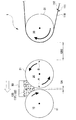
図3には,成膜工程の開始時における電極板製造装置1を示している。図3に示すように,成膜工程の開始時には,第1ロール10および第2ロール20が,第3ロール30から遠ざかる向きに移動し,離間状態とされている。図3には,この離間状態における第2対向位置Bの隙間の大きさを,GB2により示している。なお,図3に示しているGB2についても,第2対向位置Bにおける隙間の大きさの設定値である。また,GB2は,GB1よりも大きなものである。
FIG. 3 shows the electrode
また,成膜工程において形成された活物質層131は,第1ロール10の外周面11および第2ロール20の外周面21のうち,第1対向位置Aにおける移動速度が速い方の面に付着する傾向にある。そして,前述したように,電極板製造装置1においては,第2ロール20の方が,第1ロール10よりも周速の速いものである。つまり,成膜工程では,第1対向位置Aにおいて形成された活物質層131が,第2ロール20の外周面21に付着する。
Further, the
このため,第1対向位置Aを通過した第2ロール20の外周面21上には,成膜工程において形成された活物質層131が付着する。また,成膜工程において形成された活物質層131は,その後,第2ロール20の回転によって搬送され,第2対向位置Bへと到達する。
Therefore, the
図4には,成膜工程により形成された活物質層131の先端が,第2対向位置Bへと到達した後を示している。図4に示すように,第1ロール10および第2ロール20は,図3に示す離間状態より,第3ロール30へと近づく向きに移動している。この第1ロール10および第2ロール20の移動は,活物質層131の先端が第2対向位置Bへと到達後,行われたものである。また,図4に示すように,移動後の第2対向位置Bの隙間の大きさは,GB1に設定されている。
FIG. 4 shows a state after the tip of the
すなわち,本形態では,成膜工程を第2対向位置Bの隙間の大きさをGB2に設定して開始し,成膜工程により形成された活物質層131が第2対向位置Bに到達した後,第2対向位置Bの隙間の大きさをGB1に設定する隙間調整を行っている。なお,隙間調整における離間状態では,第3ロール30は回転していてもよいし,停止させていてもよい。
That is, in this embodiment, after the film forming process is started by setting the size of the gap at the second facing position B to GB2, and after the
また,第2対向位置Bには,図4に示すように,集電箔110が通されている。このため,その後,第2ロール20の回転により第2対向位置Bへと到達した活物質層131は,第3ロール30に巻き回されている集電箔110とともに,大きさGB1の隙間を通過する。その第2対向位置Bの隙間の通過の際に,集電箔110および活物質層131は,その厚み方向に第2ロール20および第3ロール30によって加圧される。
In addition, a
第2対向位置Bにおいても,加圧された活物質層131は,第2ロール20の外周面21および集電箔110の第1面111のうち,第2対向位置Bにおける移動速度が速い方に付着する傾向にある。そして,前述したように,本形態の電極板製造装置1における第3ロール30は,第2対向位置Bにおける集電箔110の第1面111の移動速度が,第2ロール20の周速よりも速くなる周速で回転している。このため,第2対向位置Bにおいて,活物質層131は,第2ロール20の外周面21上から集電箔110の第1面111上に転写される。
Even at the second facing position B, the pressurized
よって,図2に示すように,第2対向位置Bを通過後の集電箔110の第1面111には,活物質層120が転写される。そして,本形態では,集電箔110に活物質層120を転写する工程を,転写工程とする。また,隙間調整を行った以降,電極板製造装置1においては,第1ロール10,第2ロール20,第3ロール30を連続して回転させることにより,成膜工程および転写工程がともに,連続して行われることとなる。これにより,集電箔110の搬送方向における長さの長い電極板100を製造することができる。
Therefore, as shown in FIG. 2, the
ここで,本形態では,上記のように隙間調整を行うことで,集電箔110の搬送方向について均一な厚みの活物質層120を有する電極板100を製造することができる。このことについて説明する。図5は,第1対向位置Aにおいて形成される活物質層131の厚みの推移を示すグラフ図である。図5において,横軸に時間を,縦軸に第2ロール20上における活物質層131の厚みを示している。図5には,成膜工程を開始する開始時刻tSと,電極板100の製造を終了する終了時刻tEを示している。
Here, in this embodiment, the
図5のグラフより,開始時刻tSから終了時刻tEまで,成膜工程により活物質層131が形成されていることがわかる。なお,活物質層131の厚みは,成膜工程の開始時刻tSの後,一旦,T2まで厚くなり,その後,T2よりも薄いT1で推移している。つまり,図5のグラフに示すように,電極材料130が第1対向位置Aを通過し始める初期には,厚みT2の活物質層131が形成され,その後,厚みT1の厚みの活物質層131が成膜工程の終了時刻tEまで形成されている。
From the graph of FIG. 5, it can be seen that the
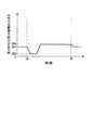
次に,図6は,本形態に係る第2対向位置Bにおける隙間の大きさの推移を示すグラフ図である。図6において,横軸に時間を,縦軸に第2対向位置Bの隙間の大きさを示している。また,図6にも,成膜工程の開始時刻tS,終了時刻tEを示している。 Next, FIG. 6 is a graph showing the transition of the size of the gap at the second facing position B according to this embodiment. In FIG. 6, the horizontal axis represents time, and the vertical axis represents the size of the gap at the second facing position B. FIG. 6 also shows the start time tS and end time tE of the film forming process.
そして,前述したように,本形態では,隙間調整を行う。このため,図6に示すように,第2対向位置Bの隙間の大きさは,開始時刻tSにおいて,GB2に設定されている。また,図6には,成膜工程により形成された第2ロール20上の活物質層131が第2対向位置Bに到達する到達時刻t1を示している。さらに,図6には,隙間調整により,第2対向位置Bの隙間の設定値をGB2からGB1とする調整時刻t2を示している。調整時刻t2は,図6に示すように,到達時刻t1よりも後である。
As described above, the gap adjustment is performed in this embodiment. For this reason, as shown in FIG. 6, the size of the gap at the second facing position B is set to GB2 at the start time tS. FIG. 6 shows an arrival time t1 when the
図6より,本形態では,調整時刻t2の後,第2対向位置Bの隙間の大きさは,設定値であるGB1で一定であることがわかる。これにより,本形態では,均一な厚みの活物質層120を有する電極板100を製造することができる。転写工程中における第2対向位置Bの隙間の大きさが,GB1で一定だからである。
As can be seen from FIG. 6, in the present embodiment, after the adjustment time t2, the size of the gap at the second facing position B is constant at the set value GB1. Thereby, in this embodiment, the
これに対し,図7には,隙間調整を行わずに成膜工程および転写工程を行った場合の第2対向位置Bにおける隙間の大きさの推移を示すグラフ図を示している。具体的に,図7は,第2対向位置Bにおける隙間の大きさの設定値をGB1で一定にしていた場合である。 On the other hand, FIG. 7 is a graph showing the transition of the size of the gap at the second facing position B when the film forming process and the transfer process are performed without adjusting the gap. Specifically, FIG. 7 shows a case where the set value of the size of the gap at the second facing position B is constant at GB1.
図7に示すように,成膜工程の開始時刻tSよりも前において,隙間の大きさは,設定値であるGB1である。しかし,開始時刻tS後,第2対向位置Bの隙間の大きさは,設定値であるGB1よりも小さいGB3まで狭くなっている。これは,第1ロール10と第2ロール20との間の第1対向位置Aの隙間を,電極材料130が通過することによるものである。
As shown in FIG. 7, the size of the gap is GB1 which is a set value before the film formation process start time tS. However, after the start time tS, the size of the gap at the second facing position B is narrowed to GB3 which is smaller than the set value GB1. This is because the
つまり,第1ロール10と第2ロール20とはそれぞれ,電極材料130を加圧するとき,その加圧に係る反力を受ける。その電極材料130を加圧する際に第1ロール10と第2ロール20とが受ける反力の向きはそれぞれ,他方から遠ざかる向きである。このため,第2ロール20は,第1ロール10から遠ざかる向きの反力を受け,第1ロール10から遠ざかる向きに移動する。
That is, when the
すなわち,第2ロール20は,電極材料130の加圧の際に,第3ロール30に近づく向きに移動する。よって,開始時刻tS後,第2対向位置Bにおける第2ロール20と第3ロール30との隙間の大きさは,第2ロール20が第3ロール30に近づく向きに移動していることにより,実際には,設定値であるGB1よりも小さいGB3まで狭くなっている。
That is, the
また,第2対向位置Bの隙間の大きさは,GB3まで狭くなった後,GB4まで広がっている。これは,電極材料130が第1対向位置Aを通過し始める初期には,厚みの厚い活物質層131が形成されており,第2ロール20の第3ロール30側への移動量が大きなものだからである。さらに,第2ロール20上の活物質層131が,第2ロール20の回転により,第2対向位置Bに到達したことによるものである。つまり,第2対向位置Bに活物質層131が到達したことにより,第2ロール20と第3ロール30とはそれぞれ,活物質層131を集電箔110とともに加圧する。このため,第2ロール20と第3ロール30とはそれぞれ,他方から遠ざかる向きの加圧に係る反力を受け,互いに遠ざかる向きに移動しているからである。
In addition, the size of the gap at the second facing position B decreases to GB3 and then increases to GB4. This is because the thick
そして,図7より,本形態に係る隙間調整を行わない場合,第2対向位置Bの隙間の大きさは,設定値であるGB1で一定ではなく,変化していることがわかる。これにより,本形態に係る隙間調整を行わない場合には,一定の厚みの活物質層120を有する電極板100を製造できないことがわかる。転写工程中における第2対向位置Bの隙間の大きさが,変化してしまうからである。
FIG. 7 shows that when the gap adjustment according to the present embodiment is not performed, the size of the gap at the second facing position B is not constant at the set value GB1 but changes. Thus, it can be seen that the
また,図7より,本形態に係る隙間調整を行わない場合には,電極板100の活物質層120を薄く形成することができないことがわかる。図7に示すように,開始時刻tS後,第2対向位置Bの隙間は設定値GB1からGB3まで狭くなっている。このため,第2対向位置Bの隙間の設定値を,GB1とGB3との差以上に設定しなければならない。第2対向位置Bの隙間の設定値を,GB1とGB3との差未満にした場合,第2ロール20と第3ロール30とが接触することとなる。これにより,第2ロール20および第3ロール30を損傷させてしまうからである。
Further, FIG. 7 shows that the
また,第2対向位置Bには,集電箔110が通されている。このため,第2ロール20と第3ロール30とが接触するような事態が生じた場合,集電箔110が挟まれて切断されてしまうからである。なお,第2対向位置Bの隙間の設定値がGB1とGB3との差以上であっても,GB3が集電箔110の厚み未満である場合には,第2ロール20と第3ロール30とによって集電箔110が強く挟み込まれてしまう。
In addition, the
これに対し,本形態では,隙間調整により,第1対向位置Aと第2対向位置Bとに加圧対象が存在する状態で第2対向位置Bの隙間を調整している。このため,本形態では,第2ロール20の加圧に伴う移動の影響を受けることなく,第2対向位置Bの隙間を調整することができる。よって,第2ロール20と第3ロール30との接触や,第2ロール20と第3ロール30とによる集電箔110の挟み込みなどが生じてしまうことを抑制できる。そして,本形態では,均一でかつ,厚みが薄い活物質層120を有する電極板100を製造することもできる。
On the other hand, in the present embodiment, the gap at the second facing position B is adjusted by the gap adjustment in a state where the pressure object exists at the first facing position A and the second facing position B. For this reason, in this embodiment, the gap at the second facing position B can be adjusted without being affected by the movement accompanying the pressurization of the
また,第2対向位置Bの隙間の大きさが同じであっても,第2ロール20の周速に対する第3ロール30の周速で表される第2ロール20と第3ロール30との周速比が低いほど,第2対向位置Bの隙間を通過後の活物質層120は薄くなる傾向にある。つまり,第2ロール20と第3ロール30との周速比は,低いほど好ましい。
In addition, even if the size of the gap at the second facing position B is the same, the circumference between the
そして,隙間調整を行わない場合には,第2ロール20と第3ロール30との周速比を低くするほど,図7に示すGB3とGB4との差が大きくなる傾向にある。つまり,隙間調整を行わない場合,電極板100における活物質層120の厚みを薄くするために第2ロール20と第3ロール30との周速比を低くすることにより,活物質層120の厚みの厚い箇所と薄い箇所との差が大きくなってしまうという問題があった。
When the gap adjustment is not performed, the difference between GB3 and GB4 shown in FIG. 7 tends to increase as the peripheral speed ratio between the
しかし,本形態では,隙間調整により第2対向位置Bの隙間の大きさを一定にすることができるため,このような問題が生じない。よって,本形態では,第2ロール20と第3ロール30との周速比を低くし,均一でかつ,厚みが薄い活物質層120を有する電極板100を製造することができる。
However, in this embodiment, such a problem does not occur because the size of the gap at the second facing position B can be made constant by adjusting the gap. Therefore, in this embodiment, the peripheral speed ratio between the
以上詳細に説明したように,本実施の形態の電極板製造装置1は,成膜工程を,第2ロール20と第3ロール30との隙間の大きさをGB1よりも大きいGB2とする離間状態として開始する。そして,成膜工程により第2ロール20上に形成された活物質層131の先端が第2対向位置Bに到達した後,その活物質層131が第2対向位置Bに存在する状態で,第2ロール20と第3ロール30との隙間の大きさをGB1とする隙間調整を行う。これにより,均一な厚みの活物質層を有する電極板の製造方法が実現されている。
As described above in detail, the electrode
なお,本実施の形態は単なる例示にすぎず,本発明を何ら限定するものではない。従って本発明は当然に,その要旨を逸脱しない範囲内で種々の改良,変形が可能である。例えば,上記の実施形態では,集電箔110の第1面111のみに活物質層120を形成する場合について説明したが,集電箔110の第2面112にも活物質層120を形成することができる。集電箔110の第2面112の活物質層120の形成についても,上記の実施形態で説明した第1面111に形成する場合と同様に行うことができる。
Note that this embodiment is merely an example, and does not limit the present invention. Therefore, the present invention can naturally be improved and modified in various ways without departing from the gist thereof. For example, in the above embodiment, the case where the
また例えば,電極材料130が活物質121,結着材122などの粉末成分に溶媒を加えたものである場合,集電箔110に活物質層120が転写された後,溶媒を除去するため,活物質層120の乾燥を行うこととすればよい。
Further, for example, when the
また例えば,上記の実施形態では,周速差により,対向位置における活物質層の付着面を制御している。しかし,第1対向位置Aにおいて形成された活物質層131は,第1ロール10の外周面11および第2ロール20の外周面21のうち,第1対向位置Aにおける曲率半径が大きい方の面に付着する傾向にある。さらに,第2対向位置Bにおいても,加圧された活物質層131は,第2ロール20の外周面21および集電箔110の第1面111のうち,第2対向位置Bにおける曲率半径が大きい方の面に付着する傾向にある。このため,上記の実施形態とは異なり,ロールの直径により,対向位置における活物質層の付着面を制御することとしてもよい。また,周速差とロールの直径との両方により,対向位置における活物質層の付着面を制御することも可能である。
Further, for example, in the above embodiment, the adhesion surface of the active material layer at the facing position is controlled by the peripheral speed difference. However, the
また例えば,上記の実施形態では,第1ロール10および第2ロール20の移動により隙間調整を行うこととして説明している。しかし,隙間調整に係る移動は,第3ロール30の移動により行うこととしてもよい。すなわち,隙間調整は,第2ロール20および第3ロール30の少なくとも一方を,他方に対して移動させることにより行うことができる。
For example, in the above embodiment, the gap adjustment is performed by moving the
また例えば,上記の実施形態に係る電極板製造装置1において,第1ロール10,第2ロール20,第3ロール30は同一の水平面内に配置されている。しかし,第1ロール10,第2ロール20,第3ロール30の配置はこれに限られるものではない。
For example, in the electrode
具体的には,例えば,図8の(a),(b),(c)それぞれに示すような配置であってもよい。図8の(a)では,第3ロール30が第2ロール20の下側に配置されている。そして,図8(a)を採用する場合,隙間調整では,第1ロール10および第2ロール20を,上向き,下向きに移動させればよい。
Specifically, for example, the arrangements shown in (a), (b), and (c) of FIG. In FIG. 8A, the
また,図8(b)では,第1ロール10が第2ロール20の下側に配置されているとともに,電極材料130が第1対向位置Aの左側より供給されるように構成されている。そして,図8(b)を採用する場合,隙間調整では,第1ロール10および第2ロール20を,左向き,右向きに移動させればよい。
Further, in FIG. 8B, the
また,図8(c)では,集電箔110が上向きに搬送されているとともに,図8(b)の構成のうちの第1ロール10,第2ロール20,仕切り部90が,集電箔110について左右対称に配置されている。この図8(c)の構成では,2つある第2ロール20がそれぞれ,上記の構成における第3ロール30としても機能するものである。また,図8(c)の構成は,集電箔110の両面について,同時に成膜工程および転写工程を行うことができるものである。そして,図8(c)を採用する場合,隙間調整では,集電箔110を挟んで設けられている第1ロール10および第2ロール20のセットを,互いに遠ざかる向き,近づく向きに移動させればよい。
Moreover, in FIG.8 (c), while the
1 電極板製造装置
10 第1ロール
20 第2ロール
30 第3ロール
100 電極板
110 集電箔
120,131 活物質層
121 活物質
122 結着材
130 電極材料
A 第1対向位置
B 第2対向位置
DESCRIPTION OF
Claims (1)
前記第2のロールと外周面の一箇所同士が前記第1の位置以外の第2の位置にて互いに対向するとともに,前記第2の位置における外周面の移動方向が第2のロールの外周面の移動方向と同じとなる向きに回転する第3のロールとを有する電極板製造装置を用い,
前記第1のロールと前記第2のロールとの隙間の大きさを第1の設定値に設定した前記第1の位置に,活物質および結着材を少なくとも含む電極材料を通過させて,前記第2のロール上に活物質層を形成する成膜工程と,
前記第2のロールと前記第3のロールとの隙間の大きさを第2の設定値に設定した前記第2の位置に,前記第2のロール上の前記活物質層を前記第3のロールに巻き回されている集電箔とともに通過させて,前記活物質層を前記集電箔上に転写して電極板となす転写工程とを有する電極板の製造方法において,
前記成膜工程を,前記第2のロールと前記第3のロールとの隙間の大きさを前記第2の設定値よりも大きな離間状態として開始し,
開始された前記成膜工程により前記第2のロール上に形成された前記活物質層の先端が前記第2の位置に到達した後,前記活物質層が前記第2の位置に存在する状態で,前記第2のロールおよび前記第3のロールの少なくとも一方を他方に向けて移動させ,前記第2のロールと前記第3のロールとの隙間の大きさを前記第2の設定値とする隙間調整を行うことを特徴とする電極板の製造方法。 A first roll and a second roll that rotate in directions in which the outer circumferential surfaces face each other and the movement directions of the outer circumferential surfaces at the first position where the outer circumferential surfaces face each other are the same;
The second roll and one outer peripheral surface are opposed to each other at a second position other than the first position, and the movement direction of the outer peripheral surface at the second position is the outer peripheral surface of the second roll. An electrode plate manufacturing apparatus having a third roll rotating in the same direction as the moving direction of
Passing an electrode material containing at least an active material and a binder to the first position where the size of the gap between the first roll and the second roll is set to a first set value, A film forming step of forming an active material layer on the second roll;
The active material layer on the second roll is moved to the third roll at the second position where the size of the gap between the second roll and the third roll is set to a second set value. In the method of manufacturing an electrode plate having a transfer step in which the active material layer is transferred onto the current collector foil and passed through the current collector foil wound around the current collector foil,
Starting the film forming step with the gap between the second roll and the third roll being in a separated state larger than the second set value;
After the tip of the active material layer formed on the second roll by the film forming process started reaches the second position, the active material layer exists in the second position. , A gap in which at least one of the second roll and the third roll is moved toward the other, and the size of the gap between the second roll and the third roll is the second set value. A method for manufacturing an electrode plate, wherein adjustment is performed.
Priority Applications (1)
| Application Number | Priority Date | Filing Date | Title |
|---|---|---|---|
| JP2015233429A JP6540480B2 (en) | 2015-11-30 | 2015-11-30 | Method of manufacturing electrode plate |
Applications Claiming Priority (1)
| Application Number | Priority Date | Filing Date | Title |
|---|---|---|---|
| JP2015233429A JP6540480B2 (en) | 2015-11-30 | 2015-11-30 | Method of manufacturing electrode plate |
Publications (2)
| Publication Number | Publication Date |
|---|---|
| JP2017103014A true JP2017103014A (en) | 2017-06-08 |
| JP6540480B2 JP6540480B2 (en) | 2019-07-10 |
Family
ID=59015570
Family Applications (1)
| Application Number | Title | Priority Date | Filing Date |
|---|---|---|---|
| JP2015233429A Active JP6540480B2 (en) | 2015-11-30 | 2015-11-30 | Method of manufacturing electrode plate |
Country Status (1)
| Country | Link |
|---|---|
| JP (1) | JP6540480B2 (en) |
Cited By (3)
| Publication number | Priority date | Publication date | Assignee | Title |
|---|---|---|---|---|
| KR20180092282A (en) * | 2017-02-08 | 2018-08-17 | 도요타 지도샤(주) | Manufacturing method of paste-layer-attached sheet and coating applicator |
| WO2023139860A1 (en) * | 2022-01-18 | 2023-07-27 | パナソニックIpマネジメント株式会社 | Stretching and conveying device for green compact |
| WO2024100985A1 (en) * | 2022-11-11 | 2024-05-16 | パナソニックIpマネジメント株式会社 | Green compact molding device and green compact molding method |
Citations (2)
| Publication number | Priority date | Publication date | Assignee | Title |
|---|---|---|---|---|
| JPH08257463A (en) * | 1995-01-24 | 1996-10-08 | Inoue Kinzoku Kogyo Kk | Coating method and device therefor |
| JP2002042789A (en) * | 2000-07-21 | 2002-02-08 | Matsushita Electric Ind Co Ltd | Method and apparatus for manufacturing battery electrode |
-
2015
- 2015-11-30 JP JP2015233429A patent/JP6540480B2/en active Active
Patent Citations (2)
| Publication number | Priority date | Publication date | Assignee | Title |
|---|---|---|---|---|
| JPH08257463A (en) * | 1995-01-24 | 1996-10-08 | Inoue Kinzoku Kogyo Kk | Coating method and device therefor |
| JP2002042789A (en) * | 2000-07-21 | 2002-02-08 | Matsushita Electric Ind Co Ltd | Method and apparatus for manufacturing battery electrode |
Cited By (7)
| Publication number | Priority date | Publication date | Assignee | Title |
|---|---|---|---|---|
| KR20180092282A (en) * | 2017-02-08 | 2018-08-17 | 도요타 지도샤(주) | Manufacturing method of paste-layer-attached sheet and coating applicator |
| KR102003155B1 (en) | 2017-02-08 | 2019-07-23 | 도요타 지도샤(주) | Manufacturing method of paste-layer-attached sheet and coating applicator |
| WO2023139860A1 (en) * | 2022-01-18 | 2023-07-27 | パナソニックIpマネジメント株式会社 | Stretching and conveying device for green compact |
| US20250091246A1 (en) * | 2022-01-18 | 2025-03-20 | Panasonic Intellectual Property Management Co., Ltd. | Stretching and conveying device for green compact |
| EP4467332A4 (en) * | 2022-01-18 | 2025-05-14 | Panasonic Intellectual Property Management Co., Ltd. | Stretching and conveying device for green compact |
| WO2024100985A1 (en) * | 2022-11-11 | 2024-05-16 | パナソニックIpマネジメント株式会社 | Green compact molding device and green compact molding method |
| EP4617049A4 (en) * | 2022-11-11 | 2026-02-18 | Panasonic Ip Man Co Ltd | GREEN COMPACT FORMING DEVICE AND GREEN COMPACT FORMING PROCESS |
Also Published As
| Publication number | Publication date |
|---|---|
| JP6540480B2 (en) | 2019-07-10 |
Similar Documents
| Publication | Publication Date | Title |
|---|---|---|
| KR101787564B1 (en) | Electrode plate manufacturing method and electrode plate manufacturing apparatus | |
| JP6210352B2 (en) | Lamination device including electrode guide | |
| CN115084443B (en) | Roller pressing device and method for manufacturing compacted strip electrode plate | |
| JP6115380B2 (en) | Strip electrode manufacturing method and strip electrode cutting apparatus | |
| US20150238994A1 (en) | Manufacturing apparatus of coating film product | |
| JP5994467B2 (en) | Method for producing lithium ion secondary battery | |
| CN105436015A (en) | Coating film, coating film production method, coating film production apparatus, nonaqueous secondary battery electrode plate, and mobile body | |
| WO2020170543A1 (en) | Non-aqueous electrolyte secondary battery, and method for manufacturing positive electrode plate used therein | |
| JP6658496B2 (en) | Electrode plate manufacturing equipment | |
| CN114270590B (en) | Method for manufacturing electrode assembly including step of simultaneously applying heat and pressure | |
| US9748577B2 (en) | Dual coating method for electrode | |
| JP6540480B2 (en) | Method of manufacturing electrode plate | |
| KR20170037100A (en) | Roll for rolling electrode and rolling apparatus comprising the same | |
| JP2017027849A (en) | Electrode plate manufacturing method | |
| JP2018026295A (en) | Electrode plate manufacturing equipment | |
| JP5796525B2 (en) | Battery electrode pressing method and pressing apparatus therefor | |
| KR101810145B1 (en) | Apparatus for pressing electrode of secondary battery | |
| JP2017174522A (en) | Electrode plate manufacturing method | |
| CN110311088B (en) | Method and apparatus for manufacturing electrode plate | |
| JP2017098176A (en) | Electrode manufacturing method | |
| JP6783668B2 (en) | Wet powder deposition method | |
| CN115275357A (en) | Pole core hot pressing equipment and battery pack | |
| CN110391397B (en) | Method for manufacturing electrode plate for lithium ion secondary battery | |
| JP6844502B2 (en) | Manufacturing method of electrode sheet with separator | |
| KR102042752B1 (en) | Apparatus for pressing electrode plate of secondary battery and Method using the same |
Legal Events
| Date | Code | Title | Description |
|---|---|---|---|
| A621 | Written request for application examination |
Free format text: JAPANESE INTERMEDIATE CODE: A621 Effective date: 20180111 |
|
| A131 | Notification of reasons for refusal |
Free format text: JAPANESE INTERMEDIATE CODE: A131 Effective date: 20181127 |
|
| A521 | Request for written amendment filed |
Free format text: JAPANESE INTERMEDIATE CODE: A523 Effective date: 20181226 |
|
| TRDD | Decision of grant or rejection written | ||
| A01 | Written decision to grant a patent or to grant a registration (utility model) |
Free format text: JAPANESE INTERMEDIATE CODE: A01 Effective date: 20190514 |
|
| A61 | First payment of annual fees (during grant procedure) |
Free format text: JAPANESE INTERMEDIATE CODE: A61 Effective date: 20190527 |
|
| R151 | Written notification of patent or utility model registration |
Ref document number: 6540480 Country of ref document: JP Free format text: JAPANESE INTERMEDIATE CODE: R151 |