JP2017107777A - Lighting device and luminaire having the same - Google Patents

Lighting device and luminaire having the same Download PDF

Info

Publication number
JP2017107777A
JP2017107777A JP2015241613A JP2015241613A JP2017107777A JP 2017107777 A JP2017107777 A JP 2017107777A JP 2015241613 A JP2015241613 A JP 2015241613A JP 2015241613 A JP2015241613 A JP 2015241613A JP 2017107777 A JP2017107777 A JP 2017107777A
Authority
JP
Japan
Prior art keywords
control circuit
switching
switching element
dimming level
lighting device
Prior art date
Legal status (The legal status is an assumption and is not a legal conclusion. Google has not performed a legal analysis and makes no representation as to the accuracy of the status listed.)
Pending
Application number
JP2015241613A
Other languages
Japanese (ja)
Inventor
駿 楠田
Shun Kusuda
駿 楠田
武志 鴨井
Takeshi Kamoi
武志 鴨井
大輔 山原
Daisuke Yamahara
大輔 山原
Current Assignee (The listed assignees may be inaccurate. Google has not performed a legal analysis and makes no representation or warranty as to the accuracy of the list.)
Panasonic Intellectual Property Management Co Ltd
Original Assignee
Panasonic Intellectual Property Management Co Ltd
Priority date (The priority date is an assumption and is not a legal conclusion. Google has not performed a legal analysis and makes no representation as to the accuracy of the date listed.)
Filing date
Publication date
Application filed by Panasonic Intellectual Property Management Co Ltd filed Critical Panasonic Intellectual Property Management Co Ltd
Priority to JP2015241613A priority Critical patent/JP2017107777A/en
Publication of JP2017107777A publication Critical patent/JP2017107777A/en
Pending legal-status Critical Current

Links

Images

Classifications

    • YGENERAL TAGGING OF NEW TECHNOLOGICAL DEVELOPMENTS; GENERAL TAGGING OF CROSS-SECTIONAL TECHNOLOGIES SPANNING OVER SEVERAL SECTIONS OF THE IPC; TECHNICAL SUBJECTS COVERED BY FORMER USPC CROSS-REFERENCE ART COLLECTIONS [XRACs] AND DIGESTS
    • Y02TECHNOLOGIES OR APPLICATIONS FOR MITIGATION OR ADAPTATION AGAINST CLIMATE CHANGE
    • Y02BCLIMATE CHANGE MITIGATION TECHNOLOGIES RELATED TO BUILDINGS, e.g. HOUSING, HOUSE APPLIANCES OR RELATED END-USER APPLICATIONS
    • Y02B20/00Energy efficient lighting technologies, e.g. halogen lamps or gas discharge lamps
    • Y02B20/40Control techniques providing energy savings, e.g. smart controller or presence detection

Landscapes

  • Circuit Arrangement For Electric Light Sources In General (AREA)

Abstract

【課題】スイッチング動作とリニア動作とを切替えることで高い調光レベルから低い調光レベルまで安定した調光を行いつつ、小型化及び製造コストの低廉化を実現することができる点灯装置及びそれを備えた照明器具を提供する。【解決手段】点灯装置2は、スイッチング素子54を用いて、入力された直流電圧を発光素子3に印加する直流電圧に変換する降圧コンバータ5と、スイッチング素子54が調光レベルに応じたスイッチング動作をする第1制御回路60と、スイッチング素子54が調光レベルに応じたリニア動作をする第2制御回路70と、調光レベルが所定値以上の場合に第1制御回路60及び第2制御回路70のうち第1制御回路60のみを動作させ、調光レベルが所定値未満の場合に第1制御回路60及び第2制御回路70のうち第2制御回路70のみを動作させる切替部81とを備えている。【選択図】図1A lighting device capable of realizing downsizing and reduction in manufacturing cost while performing stable dimming from a high dimming level to a low dimming level by switching between a switching operation and a linear operation, and a lighting device therefor Provided lighting equipment provided. A lighting device 2 uses a switching element 54 to convert an input DC voltage into a DC voltage to be applied to a light emitting element 3, and a switching operation according to a dimming level of the switching element 54. A first control circuit 60 that performs the linear operation according to the dimming level, and the first control circuit 60 and the second control circuit when the dimming level is equal to or higher than a predetermined value. A switching unit 81 that operates only the first control circuit 60 out of 70 and operates only the second control circuit 70 out of the first control circuit 60 and the second control circuit 70 when the dimming level is less than a predetermined value; I have. [Selection] Figure 1

Description

本発明は、発光ダイオード(LED:Light Emitting Diode)等の発光素子の点灯装置及びそれを備えた照明器具に関する。   The present invention relates to a lighting device for a light emitting element such as a light emitting diode (LED) and a lighting fixture including the same.

従来、発光ダイオードを用いたLED照明の点灯、調光を行う照明器具の一例としてLED照明装置が知られている(例えば特許文献1参照)。このLED照明装置に用いられているLED駆動回路が調光を行うには、定電流動作する発光素子に出力される電流値を増減させることで行われている。このLED照明装置に構成されるDC/DCコンバータの駆動方式としては、スイッチング動作(PWM制御)やリニア動作(線形駆動方式やDC駆動方式とも呼ばれる)がある。   Conventionally, an LED lighting apparatus is known as an example of a lighting fixture that performs lighting and dimming of LED lighting using a light emitting diode (see, for example, Patent Document 1). The LED drive circuit used in this LED lighting device performs light control by increasing or decreasing the current value output to the light emitting element that operates at a constant current. As a driving method of the DC / DC converter configured in the LED lighting device, there are a switching operation (PWM control) and a linear operation (also called a linear driving method or a DC driving method).

スイッチング動作は、調光信号のパルス幅を可変させることによりDC/DCコンバータから出力される平均電流値を可変させる。この方式の長所は、スイッチング素子によるオンオフの動作を繰り返すため、省エネルギーでLED照明装置を動作することができることである。一方、短所は、スイッチング素子がオンしている期間であるオン時間Tonが短くなり過ぎると、スイッチング素子が正常にオンオフの動作を行うことができず、発光素子が正常に点灯できなくなってしまうことである。また、スイッチング素子を高速にスイッチング動作することで、ノイズが発生するなどの問題もある。   In the switching operation, the average current value output from the DC / DC converter is varied by varying the pulse width of the dimming signal. The advantage of this method is that the LED lighting device can be operated with energy saving because the on / off operation by the switching element is repeated. On the other hand, the disadvantage is that if the on-time Ton, which is a period during which the switching element is on, becomes too short, the switching element cannot perform normal on / off operation, and the light emitting element cannot be normally lit. It is. Further, there is a problem that noise is generated by switching the switching element at high speed.

また、リニア動作は、発光素子に印加される電圧を可変抵抗などで変換して一定電圧を生み出し、発光素子に流れる電流を可変させる。この方式の長所は、回路の簡略化や低コスト化である。一方、短所は、可変抵抗に流れる電流に比例した電力損失が発生することである。   In the linear operation, the voltage applied to the light emitting element is converted by a variable resistor or the like to generate a constant voltage, and the current flowing through the light emitting element is varied. The advantage of this method is circuit simplification and cost reduction. On the other hand, the disadvantage is that a power loss proportional to the current flowing through the variable resistor occurs.

そこで、このLED駆動回路では、第1制御部が調光レベルの高い状態でスイッチング動作を行い、第2制御部が調光レベルの低い状態でリニア動作を行っている。   Therefore, in this LED drive circuit, the first control unit performs a switching operation with a high dimming level, and the second control unit performs a linear operation with a low dimming level.

特開2014−7078号公報Japanese Unexamined Patent Publication No. 2014-7078

しかしながら、特許文献1に記載されたLED駆動回路では、第1制御部が高い調光レベルでスイッチング動作を行い、第2制御部が低い調光レベルでリニア動作を行っている。つまり、このLED駆動回路では、スイッチング動作を行うスイッチング素子と、リニア動作を行うスイッチング素子とは、それぞれ異なるスイッチング素子を用いて制御を行っている。このため、このLED駆動回路では、部品点数の増加により、製造コストの高騰化、大型化及び電力エネルギーの増加によりランニングコストの増加が生じてしまう。   However, in the LED drive circuit described in Patent Document 1, the first control unit performs a switching operation at a high dimming level, and the second control unit performs a linear operation at a low dimming level. That is, in this LED drive circuit, the switching element that performs the switching operation and the switching element that performs the linear operation are controlled using different switching elements. For this reason, in this LED drive circuit, an increase in the number of parts causes an increase in running cost due to an increase in manufacturing cost, an increase in size, and an increase in power energy.

本発明は、このような課題を解決するためになされたものであり、スイッチング動作とリニア動作とを切替えることで高い調光レベルから低い調光レベルまで安定した調光を行いつつ、小型化及び製造コストの低廉化を実現することができる点灯装置及びそれを備えた照明器具を提供することを目的とする。   The present invention has been made to solve such a problem, and by switching between a switching operation and a linear operation, while performing stable dimming from a high dimming level to a low dimming level, downsizing and It is an object of the present invention to provide a lighting device that can realize a reduction in manufacturing cost and a lighting fixture including the lighting device.

上記課題を解決するために、本発明に係る点灯装置の一態様は、外部から指示される調光レベルに応じて発光素子に電流を流す点灯装置であって、スイッチング素子を有し、前記スイッチング素子を用いて、入力された直流電圧を前記発光素子に印加する直流電圧に変換するDC/DCコンバータと、前記スイッチング素子が前記調光レベルに応じたスイッチング動作をするように前記スイッチング素子を制御する第1制御回路と、前記スイッチング素子が前記調光レベルに応じたリニア動作をするように前記スイッチング素子を制御する第2制御回路と、前記調光レベルが所定値以上の場合に前記第1制御回路及び前記第2制御回路のうち前記第1制御回路のみを動作させ、前記調光レベルが所定値未満の場合に前記第1制御回路及び前記第2制御回路のうち前記第2制御回路のみを動作させる切替回路とを備える。   In order to solve the above-described problem, one aspect of a lighting device according to the present invention is a lighting device that allows a current to flow through a light-emitting element in accordance with a dimming level that is instructed from the outside. A DC / DC converter that converts an input DC voltage into a DC voltage to be applied to the light emitting element, and the switching element is controlled so that the switching element performs a switching operation according to the dimming level. A first control circuit that controls the switching element so that the switching element performs a linear operation according to the dimming level, and the first control circuit when the dimming level is a predetermined value or more. Of the control circuit and the second control circuit, only the first control circuit is operated, and when the dimming level is less than a predetermined value, the first control circuit and the second control circuit And a switching circuit for operating only said second control circuit of the two control circuits.

本発明によれば、スイッチング動作とリニア動作とを切替えることで高い調光レベルから低い調光レベルまで安定した調光を行いつつ、小型化及び製造コストの低廉化を実現することができる。   According to the present invention, it is possible to realize downsizing and reduction in manufacturing cost while performing stable dimming from a high dimming level to a low dimming level by switching between a switching operation and a linear operation.

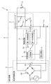
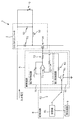
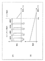
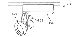
実施の形態1における点灯装置及びそれを備えた照明器具の構成を示す回路図である。It is a circuit diagram which shows the structure of the lighting device in Embodiment 1, and a lighting fixture provided with the same. 実施の形態1における点灯装置の制御部及びDC/DCコンバータの構成を示す回路図である。FIG. 3 is a circuit diagram illustrating a configuration of a control unit and a DC / DC converter of the lighting device in the first embodiment. (A)は、実施の形態1における点灯装置のスイッチング素子の動作を示すタイミング図である。(B)は、実施の形態1における点灯装置のインダクタの動作を示すタイミング図である。(C)は、実施の形態1における点灯装置のダイオードの動作を示すタイミング図である。(A) is a timing chart which shows operation | movement of the switching element of the lighting device in Embodiment 1. FIG. (B) is a timing chart showing the operation of the inductor of the lighting device in the first embodiment. (C) is a timing chart showing the operation of the diode of the lighting device in the first embodiment. (A)は、実施の形態1における点灯装置のスイッチング素子の電圧と調光レベルとの関係を示すタイミング図である。(B)は、実施の形態1における点灯装置のスイッチング素子の電流と調光レベルとの関係を示すタイミング図である。(A) is a timing diagram which shows the relationship between the voltage of the switching element of the lighting device in Embodiment 1, and a light control level. (B) is a timing chart showing the relationship between the current of the switching element of the lighting device and the dimming level in the first embodiment. (A)は、実施の形態1の変形例1における点灯装置のスイッチング素子の電圧と調光レベルとの関係を示すタイミング図である。(B)は、実施の形態1の変形例1における点灯装置のスイッチング素子の電流と調光レベルとの関係を示すタイミング図である。(A) is a timing chart showing the relationship between the voltage of the switching element of the lighting device and the dimming level in Modification 1 of Embodiment 1. FIG. (B) is a timing chart showing the relationship between the current of the switching element of the lighting device and the dimming level in Modification 1 of Embodiment 1. FIG. (A)は、実施の形態1の変形例2における点灯装置のスイッチング素子の電圧と調光レベルとの関係を示すタイミング図である。(B)は、実施の形態1の変形例2における点灯装置のスイッチング素子の電流と調光レベルとの関係を示すタイミング図である。(A) is a timing diagram which shows the relationship between the voltage of the switching element of the lighting device in the modification 2 of Embodiment 1, and a light control level. (B) is a timing chart showing the relationship between the current of the switching element of the lighting device and the dimming level in Modification 2 of Embodiment 1. FIG. 実施の形態2における点灯装置の一部の構成を示す回路図である。FIG. 6 is a circuit diagram illustrating a partial configuration of a lighting device according to Embodiment 2. 実施の形態2における点灯装置の動作を示すグラフである。6 is a graph showing the operation of the lighting device in the second embodiment. 実施の形態3における点灯装置の制御部及びDC/DCコンバータの構成を示す回路図である。FIG. 6 is a circuit diagram illustrating a configuration of a control unit and a DC / DC converter of a lighting device in a third embodiment. 実施の形態4における照明器具の外観図である。14 is an external view of a lighting fixture in Embodiment 4. FIG. 実施の形態4における照明器具の外観図である。14 is an external view of a lighting fixture in Embodiment 4. FIG. 実施の形態4における照明器具の外観図である。14 is an external view of a lighting fixture in Embodiment 4. FIG.

以下、本発明の実施の形態について、図面を参照しながら説明する。以下に説明する実施の形態は、いずれも本発明の好ましい一具体例を示すものである。したがって、以下の実施の形態で示される数値、形状、材料、構成要素、構成要素の配置位置及び接続形態などは、一例であって本発明を限定する主旨ではない。よって、以下の実施の形態における構成要素のうち、本発明の最上位概念を示す独立請求項に記載されていない構成要素については、任意の構成要素として説明される。   Hereinafter, embodiments of the present invention will be described with reference to the drawings. Each of the embodiments described below shows a preferred specific example of the present invention. Therefore, the numerical values, shapes, materials, components, arrangement positions and connection forms of the components shown in the following embodiments are merely examples, and are not intended to limit the present invention. Therefore, among the constituent elements in the following embodiments, constituent elements that are not described in the independent claims showing the highest concept of the present invention are described as optional constituent elements.

なお、各図は、模式図であり、必ずしも厳密に図示されたものではない。また、各図において、実質的に同一の構成に対しては同一の符号を付しており、重複する説明は省略又は簡略化する。   Each figure is a schematic diagram and is not necessarily illustrated strictly. Moreover, in each figure, the same code | symbol is attached | subjected to the substantially same structure, The overlapping description is abbreviate | omitted or simplified.

(実施の形態1)
[構成]
以下、本発明の実施の形態1に係る点灯装置の構成について、図1を用いて説明する。
(Embodiment 1)
[Constitution]
Hereinafter, the structure of the lighting device according to Embodiment 1 of the present invention will be described with reference to FIG.

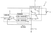
図1は、実施の形態1における点灯装置及びそれを備えた照明器具の構成を示す回路図である。   1 is a circuit diagram illustrating a configuration of a lighting device and a lighting fixture including the lighting device according to Embodiment 1. FIG.

図1に示されるように、照明器具1は、点灯装置2と、発光素子3とを有している。   As illustrated in FIG. 1, the lighting fixture 1 includes a lighting device 2 and a light emitting element 3.

点灯装置2は、外部から指示される調光レベル(光出力)に応じて発光素子3に電流を流す。点灯装置2は、直流電源回路4と、降圧コンバータ5(DC/DCコンバータの一例)と、制御回路6と、切替回路8と、調光回路9とを備えている。なお、調光レベルとは、発光素子3の明るさを調整するための変数であり、数値が大きいほど(最大値は100%)、発光素子3の明るさを増加させることができる。また、調光レベルは、例えば、調光率、調光比などと表現することもある。   The lighting device 2 supplies a current to the light emitting element 3 in accordance with a dimming level (light output) instructed from the outside. The lighting device 2 includes a DC power supply circuit 4, a step-down converter 5 (an example of a DC / DC converter), a control circuit 6, a switching circuit 8, and a dimming circuit 9. Note that the dimming level is a variable for adjusting the brightness of the light-emitting element 3, and the brightness of the light-emitting element 3 can be increased as the numerical value increases (the maximum value is 100%). The dimming level may be expressed as a dimming rate, a dimming ratio, or the like, for example.

直流電源回路4は、降圧コンバータ5に入力する直流電圧を生成する。直流電源回路4は、交流電源41と、ダイオードブリッジ42と、コンデンサ43とを有している。   The DC power supply circuit 4 generates a DC voltage that is input to the step-down converter 5. The DC power supply circuit 4 includes an AC power supply 41, a diode bridge 42, and a capacitor 43.

交流電源41は、ダイオードブリッジ42に交流電圧を出力する電源であり、例えば、商用交流電源などの系統電源である。   The AC power supply 41 is a power supply that outputs an AC voltage to the diode bridge 42, and is a system power supply such as a commercial AC power supply.

ダイオードブリッジ42及びコンデンサ43は、商用交流電源などの交流電源41から供給される交流電圧を整流及び平滑化し、直流電圧に変換する整流平滑回路であり、この直流電圧を降圧コンバータ5に入力する。ダイオードブリッジ42の入力端子間には、交流電源41が接続されている。ダイオードブリッジ42の出力端子間には、平滑化用のコンデンサ43が接続されている。   The diode bridge 42 and the capacitor 43 are a rectifying / smoothing circuit that rectifies and smoothes an AC voltage supplied from an AC power source 41 such as a commercial AC power source, and converts the DC voltage into a DC voltage. The DC voltage is input to the step-down converter 5. An AC power supply 41 is connected between the input terminals of the diode bridge 42. A smoothing capacitor 43 is connected between the output terminals of the diode bridge 42.

降圧コンバータ5は、スイッチング素子54を用いて、整流平滑回路から入力された直流電圧を、所定の直流電圧に変換して発光素子3に印加する回路である。降圧コンバータ5は、入力された直流電圧をチョッピングするチョッパ回路を構成している。降圧コンバータ5は、ダイオード51と、インダクタ52と、コンデンサ53と、スイッチング素子54とを有している。   The step-down converter 5 is a circuit that converts the DC voltage input from the rectifying and smoothing circuit into a predetermined DC voltage using the switching element 54 and applies it to the light emitting element 3. The step-down converter 5 constitutes a chopper circuit that chops the input DC voltage. The step-down converter 5 includes a diode 51, an inductor 52, a capacitor 53, and a switching element 54.

ダイオード51は、インダクタ52に蓄積されたエネルギーを回生させる。ダイオード51のアノード電極は、インダクタ52の一端側の端子と、スイッチング素子54のドレイン電極とに接続されている。ダイオード51のカソード電極は、ダイオードブリッジ42及びコンデンサ43で構成される整流平滑回路の高電位側の出力端子と、コンデンサ53の一端側の端子と、発光素子3のアノード電極とに接続されている。   The diode 51 regenerates energy stored in the inductor 52. The anode electrode of the diode 51 is connected to the terminal on one end side of the inductor 52 and the drain electrode of the switching element 54. The cathode electrode of the diode 51 is connected to the output terminal on the high potential side of the rectifying / smoothing circuit including the diode bridge 42 and the capacitor 43, the terminal on one end side of the capacitor 53, and the anode electrode of the light emitting element 3. .

インダクタ52の一端側の端子も、さらに、スイッチング素子54のドレイン電極に接続されている。インダクタ52の他端側の端子は、コンデンサ53の他端側の端子と、発光素子3のカソード電極とに接続されている。   A terminal on one end side of the inductor 52 is also connected to the drain electrode of the switching element 54. The terminal on the other end side of the inductor 52 is connected to the terminal on the other end side of the capacitor 53 and the cathode electrode of the light emitting element 3.

コンデンサ53は、発光素子3と並列に接続している。コンデンサ53は、ダイオード51、インダクタ52及びコンデンサ53で構成している点灯回路で発生する出力電圧及び出力電流を平滑化する。   The capacitor 53 is connected in parallel with the light emitting element 3. Capacitor 53 smoothes the output voltage and output current generated in the lighting circuit composed of diode 51, inductor 52, and capacitor 53.

スイッチング素子54は、MOSFET(Metal−Oxide Semiconductor Field−Effect Transistor)等の素子である。本実施の形態では、スイッチング素子54は、nチャネル型のMOSFETである。スイッチング素子54のソース電極には、抵抗11の一端側の端子と、制御回路6とが接続されている。スイッチング素子54のゲート電極には、制御回路6が接続されている。スイッチング素子54は、制御回路6から出力された制御信号に基づいてダイオード51及びインダクタ52と抵抗11との間をオンオフする。   The switching element 54 is an element such as a MOSFET (Metal-Oxide Semiconductor Field-Effect Transistor). In the present embodiment, the switching element 54 is an n-channel MOSFET. A terminal on one end side of the resistor 11 and the control circuit 6 are connected to the source electrode of the switching element 54. A control circuit 6 is connected to the gate electrode of the switching element 54. The switching element 54 turns on and off between the diode 51 and the inductor 52 and the resistor 11 based on the control signal output from the control circuit 6.

抵抗11は、スイッチング素子54と直列に接続され、スイッチング素子54に流れる電流を検出する電流検出用の抵抗である。この抵抗11の他端側の端子は、グランドに接続されている。この抵抗11は、スイッチング素子54の出力電流を検出する。この検出された電流値は、制御回路6に入力される。   The resistor 11 is a current detection resistor that is connected in series with the switching element 54 and detects a current flowing through the switching element 54. The terminal on the other end side of the resistor 11 is connected to the ground. This resistor 11 detects the output current of the switching element 54. The detected current value is input to the control circuit 6.

調光回路9は、制御回路6に、切替回路8を介して調光信号を入力する回路である。調光回路9は、例えば、図示しないリモコンなどによる外部から信号を受信し、発光素子3が所望の光出力をすることができるように調光信号を算出する。つまり、調光回路9は、調光レベルに応じた調光信号を決定している。   The dimming circuit 9 is a circuit that inputs a dimming signal to the control circuit 6 via the switching circuit 8. The dimming circuit 9 receives a signal from the outside, for example, by a remote controller (not shown), and calculates a dimming signal so that the light emitting element 3 can output a desired light. That is, the dimming circuit 9 determines the dimming signal according to the dimming level.

調光信号は、発光素子3の調光レベルを指定する信号であり、例えば、直流電圧、又は、PWM信号等である。本実施の形態では、調光信号は、PWM信号であるとして説明している。PWM信号は、スイッチング素子54をPWM制御により駆動させるための矩形波状の電圧波形を有する信号である。   The dimming signal is a signal that specifies the dimming level of the light emitting element 3, and is, for example, a DC voltage or a PWM signal. In the present embodiment, the dimming signal is described as being a PWM signal. The PWM signal is a signal having a rectangular wave voltage waveform for driving the switching element 54 by PWM control.

切替回路8は、切替部81と、スイッチ82とを有している。切替部81の入力側は、調光回路9に接続されている。切替部81の出力側は、スイッチ82に接続されている。切替部81は、調光レベルに応じてスイッチ82を後述する第1制御回路60か後述する第2制御回路70かに切替える。   The switching circuit 8 includes a switching unit 81 and a switch 82. The input side of the switching unit 81 is connected to the dimming circuit 9. The output side of the switching unit 81 is connected to the switch 82. The switching unit 81 switches the switch 82 to a first control circuit 60 described later or a second control circuit 70 described later according to the dimming level.

切替回路8は、調光回路9から出力された調光信号を制御回路6に入力する。切替回路8は、調光レベルが所定値以上の場合に第1制御回路60及び第2制御回路70のうち第1制御回路60のみを動作させ、調光レベルが所定値未満の場合に第1制御回路60及び第2制御回路70のうち第2制御回路70のみを動作させる。つまり、切替部81は、調光レベルに対応するオン時間Tonが所定時間以上か未満かを判断することで、スイッチ82を切替えて第1制御回路60及び第2制御回路70のいずれか一方のみを動作させる。本実施の形態では、切替回路8は、直流電圧に行うローパスフィルタを有し、調光回路9から入力された調光信号(PWM信号)を平滑化して出力する。   The switching circuit 8 inputs the dimming signal output from the dimming circuit 9 to the control circuit 6. The switching circuit 8 operates only the first control circuit 60 out of the first control circuit 60 and the second control circuit 70 when the dimming level is equal to or higher than a predetermined value, and first when the dimming level is lower than the predetermined value. Of the control circuit 60 and the second control circuit 70, only the second control circuit 70 is operated. That is, the switching unit 81 determines whether the on-time Ton corresponding to the dimming level is equal to or longer than the predetermined time, thereby switching the switch 82 and only one of the first control circuit 60 and the second control circuit 70. To work. In the present embodiment, the switching circuit 8 has a low-pass filter for DC voltage, and smoothes and outputs the dimming signal (PWM signal) input from the dimming circuit 9.

制御回路6は、切替回路8を介して調光回路9が出力した調光信号をスイッチング素子54のゲート電極に供給する。制御回路6は、第1制御回路60及び第2制御回路70を有している。   The control circuit 6 supplies the dimming signal output from the dimming circuit 9 via the switching circuit 8 to the gate electrode of the switching element 54. The control circuit 6 includes a first control circuit 60 and a second control circuit 70.

図2は、実施の形態1における点灯装置の制御部及び降圧コンバータの構成を示す回路図である。   FIG. 2 is a circuit diagram showing a configuration of a control unit and a step-down converter of the lighting device in the first embodiment.

図2に示すように、制御回路6の第1制御回路60は、調光回路9から切替回路8を介して入力される調光信号に応じて発光素子3に流れる電流が変化するようにスイッチング素子54のオンオフ又は導通抵抗を制御する。第1制御回路60は、スイッチング素子54が調光レベルに応じたスイッチング動作をするようにスイッチング素子54を制御する。第1制御回路60は、パルス電源61と抵抗62とを有している。   As shown in FIG. 2, the first control circuit 60 of the control circuit 6 performs switching so that the current flowing through the light emitting element 3 changes according to the dimming signal input from the dimming circuit 9 via the switching circuit 8. The on / off or conduction resistance of the element 54 is controlled. The first control circuit 60 controls the switching element 54 so that the switching element 54 performs a switching operation according to the dimming level. The first control circuit 60 includes a pulse power supply 61 and a resistor 62.

パルス電源61は、抵抗62を介してスイッチング素子54のゲート電極に接続されている。パルス電源61は、調光回路9から切替回路8を介して入力される調光信号を、調光信号に応じてオン時間Ton又はオフ時間Toffを変更したり、周波数を変更したりするような、矩形波状の調光信号をスイッチング素子54のゲート電極に出力する。   The pulse power supply 61 is connected to the gate electrode of the switching element 54 via the resistor 62. The pulse power supply 61 changes the on time Ton or the off time Toff or changes the frequency of the dimming signal input from the dimming circuit 9 via the switching circuit 8 according to the dimming signal. A rectangular wave-shaped dimming signal is output to the gate electrode of the switching element 54.

具体的には、調光回路9から出力された調光信号は切替回路8で平滑化され、パルス電源61には、この平滑化した信号(直流電圧)が入力される。パルス電源61は、発光素子3に流れる電流(ドレイン電流)が一定となるように、調光回路9から入力された調光信号に応じ、自らがスイッチング素子54のゲート電極に発する調光信号の幅を調節する。ここにおいて、調光信号の幅を変化させると、スイッチング素子54がオンオフの繰り返しにおけるオン時間Tonの割合(オンデューティ)が変化する。つまり、スイッチング素子54は、調光信号によってオンオフのタイミングが決定される。   Specifically, the dimming signal output from the dimming circuit 9 is smoothed by the switching circuit 8, and the smoothed signal (DC voltage) is input to the pulse power supply 61. In response to the dimming signal input from the dimming circuit 9, the pulse power supply 61 emits a dimming signal to the gate electrode of the switching element 54 so that the current (drain current) flowing through the light emitting element 3 is constant. Adjust the width. Here, when the width of the dimming signal is changed, the ratio (on duty) of the on time Ton when the switching element 54 is repeatedly turned on and off changes. That is, the on / off timing of the switching element 54 is determined by the dimming signal.

第2制御回路70は、スイッチング素子54が調光レベルに応じたリニア動作をするようにスイッチング素子54を制御する。第2制御回路70は、オペアンプ71と、抵抗72、73と、コンデンサ74とを備えている。   The second control circuit 70 controls the switching element 54 so that the switching element 54 performs a linear operation according to the dimming level. The second control circuit 70 includes an operational amplifier 71, resistors 72 and 73, and a capacitor 74.

オペアンプ71の非反転入力端子には切替回路8で平滑された電圧が入力され、反転入力端子には抵抗73に印加される電圧が入力される。また、オペアンプ71の出力端子は、抵抗72を介してスイッチング素子54のゲート電極に接続されている。さらに、オペアンプ71の出力端子と非反転入力端子とは、コンデンサ74を介して接続されている。つまり、オペアンプ71は、フィードバック経路(スイッチング素子54のソース電極から制御回路6に向かう経路)に抵抗72、スイッチング素子54及び抵抗73が接続されたボルテージフォロワを構成している。言い換えれば、オペアンプ71は、非反転入力端子に調光信号(直流電圧)が入力されると、非反転入力端子と反転入力端子とがイマジナリショートとなるようにスイッチング素子54を駆動する(導通抵抗を制御する)。   The voltage smoothed by the switching circuit 8 is input to the non-inverting input terminal of the operational amplifier 71, and the voltage applied to the resistor 73 is input to the inverting input terminal. The output terminal of the operational amplifier 71 is connected to the gate electrode of the switching element 54 via the resistor 72. Further, the output terminal of the operational amplifier 71 and the non-inverting input terminal are connected via a capacitor 74. That is, the operational amplifier 71 constitutes a voltage follower in which the resistor 72, the switching element 54, and the resistor 73 are connected to the feedback path (path from the source electrode of the switching element 54 to the control circuit 6). In other words, when the dimming signal (DC voltage) is input to the non-inverting input terminal, the operational amplifier 71 drives the switching element 54 so that the non-inverting input terminal and the inverting input terminal are short-circuited (conduction resistance). Control).

発光素子3は、点灯回路から直流電流が入力される素子であり、降圧コンバータ5から供給される直流電圧により発光する。発光素子3は、例えば、LED、有機EL(Electro−Luminescence)などである。なお、発光素子3は、直列接続された複数のLEDから構成されてもよい。発光素子3は、1つに限らず、2以上であってもよい。   The light emitting element 3 is an element to which a direct current is input from the lighting circuit, and emits light by a direct current voltage supplied from the step-down converter 5. The light emitting element 3 is, for example, an LED or an organic EL (Electro-Luminescence). In addition, the light emitting element 3 may be comprised from several LED connected in series. The number of light emitting elements 3 is not limited to one and may be two or more.

[動作]
次に、本発明の実施の形態1に係る点灯装置2の動作について説明する。
[Operation]
Next, the operation of the lighting device 2 according to Embodiment 1 of the present invention will be described.

図3の(A)は、実施の形態1における点灯装置のスイッチング素子の動作を示すタイミング図である。図3の(B)は、実施の形態1における点灯装置のインダクタの動作を示すタイミング図である。図3の(C)は、実施の形態1における点灯装置のダイオードの動作を示すタイミング図である。   FIG. 3A is a timing chart showing the operation of the switching element of the lighting device in the first embodiment. FIG. 3B is a timing chart showing the operation of the inductor of the lighting device in the first embodiment. FIG. 3C is a timing chart showing the operation of the diode of the lighting device in the first embodiment.

図3の(A)は、スイッチング素子54に印加される電圧と時間との関係を示している。図3の(B)は、インダクタ52に流れる電流と時間との関係を示している。図3の(C)は、ダイオード51に印加される電圧と時間との関係を示している。図3に示す太い実線は、図3の(A)ではスイッチング素子54に印加される電圧、図3の(B)ではインダクタ52に流れる電流、図3の(C)では降圧コンバータ5に入力される電圧の波形を示している。図3に示す細い実線は、図3の(B)ではインダクタ52から出力される出力電流を示し、図3の(C)ではダイオード51から出力される出力電圧を示している。インダクタ52から出力される出力電流は、三角波形状に示されている電流のピーク値の1/2の値で求められる。ダイオード51から出力される出力電圧は、オン時間Tonと、1周期Tと、ダイオード51の電圧のピーク値である入力電圧Eiとにより、以下の式で表すことができる。   FIG. 3A shows the relationship between the voltage applied to the switching element 54 and time. FIG. 3B shows the relationship between the current flowing through the inductor 52 and time. FIG. 3C shows the relationship between the voltage applied to the diode 51 and time. The thick solid line shown in FIG. 3 is a voltage applied to the switching element 54 in FIG. 3A, a current flowing through the inductor 52 in FIG. 3B, and input to the step-down converter 5 in FIG. This shows the voltage waveform. 3 indicates the output current output from the inductor 52 in FIG. 3B and the output voltage output from the diode 51 in FIG. 3C. The output current output from the inductor 52 is obtained by a value that is ½ of the peak value of the current shown in the triangular wave shape. The output voltage output from the diode 51 can be expressed by the following expression using the ON time Ton, one period T, and the input voltage Ei that is the peak value of the voltage of the diode 51.

ダイオードの出力電圧=(Ton/T)×Ei   Diode output voltage = (Ton / T) × Ei

図2及び図3の(A)に示すように、パルス電源61は、調光回路9が切替回路8を介して入力された調光信号を降圧コンバータ5に入力する。ここで、スイッチング素子54が1回ずつ行うオンオフの動作を1周期とする。図3の(A)では、この調光信号は、デューティ比を示すオン時間Tonと、オフ時間Toffとから構成される。例えば、50%のデューティ比をもつ調光信号を生成している。ここで、デューティ比とは、調光信号における1周期に占めるオン時間Tonの割合である。   As shown in FIG. 2 and FIG. 3A, the pulse power supply 61 inputs the dimming signal input from the dimming circuit 9 through the switching circuit 8 to the step-down converter 5. Here, an on / off operation performed once by the switching element 54 is defined as one cycle. In FIG. 3A, the dimming signal includes an on-time Ton indicating a duty ratio and an off-time Toff. For example, a dimming signal having a duty ratio of 50% is generated. Here, the duty ratio is a ratio of the on-time Ton occupying one cycle in the dimming signal.

次に、制御回路6の第1制御回路60がスイッチング動作をする場合の点灯装置2の動作について説明する。   Next, the operation of the lighting device 2 when the first control circuit 60 of the control circuit 6 performs a switching operation will be described.

図2及び図3の(A)に示すように、第1制御回路60のスイッチング動作は、オン時間Tonが所定時間以上(高輝度領域での駆動)の場合である。第1制御回路60は、調光回路9で生成された調光信号が切替回路8を介して入力されると、降圧コンバータ5に入力する電流をパルス駆動させる。つまり、スイッチング素子54は、入力された調光信号により、オンオフを繰り返す。スイッチング素子54がオン時間Tonのときには、交流電源41が直流電源回路4で直流にされた電流が発光素子3に流れる。一方、スイッチング素子54がオフ時間Toffのときには、インダクタ52に蓄積されていたエネルギーが回生電流となってダイオード51を介して発光素子3に流れる。このような動作により、図3の(A)に示されるような波形の電圧が生じる。   As shown in FIG. 2 and FIG. 3A, the switching operation of the first control circuit 60 is when the on-time Ton is longer than a predetermined time (driving in a high luminance region). When the dimming signal generated by the dimming circuit 9 is input via the switching circuit 8, the first control circuit 60 pulses the current input to the step-down converter 5. That is, the switching element 54 is repeatedly turned on and off by the input dimming signal. When the switching element 54 is in the on-time Ton, a current that has been changed to direct current by the AC power supply 41 by the DC power supply circuit 4 flows to the light emitting element 3. On the other hand, when the switching element 54 is off time Toff, the energy accumulated in the inductor 52 becomes a regenerative current and flows to the light emitting element 3 through the diode 51. Such an operation generates a voltage having a waveform as shown in FIG.

図1及び図3の(B)に示すように、インダクタ52に流れる電流は、図3の(A)に示す調光信号の波形に対応した波形をもつ。インダクタ52に流れる電流は、スイッチング素子54がオン時間Tonのときにその高さが次第に大きくなる続く立ち上がり期間と、スイッチング素子54がオフ時間Toffのときにその高さが次第に小さくなる立ち下り期間とからなる。具体的には、スイッチング素子54がオン時間Tonである場合に、発光素子3、インダクタ52、スイッチング素子54及び抵抗11に電流が流れ、インダクタ52に流れる電流が増加する。一方、スイッチング素子54がオフ時間Toffである場合に、インダクタ52に蓄積されていたエネルギーがダイオード51を介して放出されることで、インダクタ52、ダイオード51及び発光素子3に電流が流れる。すると、インダクタ52に流れる電流は次第に減少していく。こうして、スイッチング素子54のスイッチングにより、インダクタ52には、一定周期の三角波形状の電流が流れる。   As shown in FIGS. 1 and 3B, the current flowing through the inductor 52 has a waveform corresponding to the waveform of the dimming signal shown in FIG. The current flowing through the inductor 52 includes a rising period in which the height gradually increases when the switching element 54 is on-time Ton, and a falling period in which the height gradually decreases when the switching element 54 is off-time Toff. Consists of. Specifically, when the switching element 54 is on-time Ton, a current flows through the light emitting element 3, the inductor 52, the switching element 54 and the resistor 11, and the current flowing through the inductor 52 increases. On the other hand, when the switching element 54 has the off time Toff, the energy stored in the inductor 52 is released through the diode 51, so that a current flows through the inductor 52, the diode 51, and the light emitting element 3. Then, the current flowing through the inductor 52 gradually decreases. In this way, a triangular wave current having a constant period flows through the inductor 52 by switching of the switching element 54.

図1及び図3の(C)に示すように、ダイオード51に流れる電流は、スイッチング素子54がオフであるときに、インダクタ52に蓄積されていたエネルギーの放出による。そして、インダクタ52、ダイオード51及び発光素子3に電流が流れる。一方、スイッチング素子54がオン時間Tonである場合は、発光素子3、インダクタ52、スイッチング素子54及び抵抗11に電流が流れ、ダイオード51に電流は流れない。こうして、発光素子3は、オフ時間Toffでもコンデンサ53の平滑化により、一定の出力電流が発光素子3に供給され、発光し続ける。このような動作により、図3の(C)に示されるような波形の電圧が生じる。   As shown in FIGS. 1 and 3C, the current flowing through the diode 51 is due to the release of energy stored in the inductor 52 when the switching element 54 is off. A current flows through the inductor 52, the diode 51, and the light emitting element 3. On the other hand, when the switching element 54 is on-time Ton, a current flows through the light emitting element 3, the inductor 52, the switching element 54 and the resistor 11, and no current flows through the diode 51. In this way, the light emitting element 3 continues to emit light even when the off time Toff is applied, by supplying a constant output current to the light emitting element 3 by smoothing the capacitor 53. By such an operation, a voltage having a waveform as shown in FIG.

図4の(A)は、実施の形態1における点灯装置のスイッチング素子の電圧と調光レベルとの関係を示すタイミング図である。図4の(B)は、実施の形態1における点灯装置のスイッチング素子の電流と調光レベルとの関係を示すタイミング図である。   FIG. 4A is a timing chart showing the relationship between the voltage of the switching element of the lighting device and the dimming level in the first embodiment. FIG. 4B is a timing chart showing the relationship between the current of the switching element of the lighting device and the dimming level in the first embodiment.

図4の(A)では、スイッチング素子54のゲート電極にかかる電圧と調光レベルとを示すグラフである。図4の(B)では、スイッチング素子54のゲート電極にかかる電流と調光レベルとを示すグラフである。図4は、オン時間Tonが所定時間以上である場合にスイッチング動作を行い、オン時間Tonが所定時間未満である場合にリニア動作を行う。また、図4において、図4の(A)と図4の(B)とは対応している。例えば、図4の(A)の1周期当たりの電圧と図4の(B)の電流とが対応しており、調光レベルが5%の場合とオン時間Tonの所定時間の場合とが対応している。   FIG. 4A is a graph showing the voltage applied to the gate electrode of the switching element 54 and the dimming level. FIG. 4B is a graph showing the current applied to the gate electrode of the switching element 54 and the dimming level. In FIG. 4, the switching operation is performed when the on-time Ton is equal to or longer than the predetermined time, and the linear operation is performed when the on-time Ton is less than the predetermined time. Further, in FIG. 4, (A) in FIG. 4 corresponds to (B) in FIG. For example, the voltage per cycle in FIG. 4A corresponds to the current in FIG. 4B, and the dimming level is 5% and the on-time Ton is a predetermined time. doing.

図1及び図4に示すように、切替部81は、オン時間Tonが所定時間以上か未満化を判断する。所定時間とは、スイッチング素子54がスイッチング動作を安定して動作でき難くなる時間を意味している。この所定時間は、スイッチング素子54の性能に依存している。切替回路8は、オン時間Tonが所定時間以上である場合は、第1制御回路60を動作させる。   As shown in FIGS. 1 and 4, the switching unit 81 determines whether the on time Ton is equal to or longer than a predetermined time. The predetermined time means a time during which the switching element 54 becomes difficult to operate stably. This predetermined time depends on the performance of the switching element 54. The switching circuit 8 operates the first control circuit 60 when the on-time Ton is equal to or longer than the predetermined time.

図4の(A)及び図4の(B)に示すように、第1制御回路60のパルス電源61は、調光レベルに応じて、スイッチング素子54のオンオフの繰り返しにおけるオン時間Tonを変化させることで、スイッチング素子54を制御する。つまり、第1制御回路60のパルス電源61は、スイッチング素子54がオンオフを行う各周期を同一にする。そして、1周期当たりのスイッチング素子54のオン時間Tonの割合を変化させることで、スイッチング素子54のデューティ比を変えて発光素子3の調光レベル(明るさ)を調節する。   As shown in FIGS. 4A and 4B, the pulse power supply 61 of the first control circuit 60 changes the ON time Ton in the ON / OFF repetition of the switching element 54 according to the dimming level. Thus, the switching element 54 is controlled. In other words, the pulse power supply 61 of the first control circuit 60 sets the same period for turning on and off the switching element 54. Then, the dimming level (brightness) of the light emitting element 3 is adjusted by changing the duty ratio of the switching element 54 by changing the ratio of the ON time Ton of the switching element 54 per cycle.

具体的には、第1制御回路60は、スイッチング素子54がオンオフを行う各周期を同一にした状態で、調光レベルを低下する場合に、スイッチング素子54のオン時間Tonを短くし、スイッチング素子54のオフ時間Toffを長くさせる。この場合、デューティ比は減少する。発光素子3では、1周期当たり、オン時間Tonの割合が短くなるとともにオフ時間Toffの割合が長くなり、調光レベルが低い状態となる。また、第1制御回路60は、発光素子3の調光レベルを上昇させる場合に、1周期当たり、スイッチング素子54のオン時間Tonの割合を長くし、スイッチング素子54のオフ時間Toffの割合を短くさせてデューティ比を上昇させる。   Specifically, the first control circuit 60 shortens the on-time Ton of the switching element 54 when the dimming level is lowered in the state where the switching elements 54 are turned on and off at the same period. The off time Toff of 54 is lengthened. In this case, the duty ratio decreases. In the light emitting element 3, the ratio of the on time Ton is shortened and the ratio of the off time Toff is increased per cycle, and the light control level is low. Further, when increasing the dimming level of the light emitting element 3, the first control circuit 60 increases the ratio of the on time Ton of the switching element 54 and shortens the ratio of the off time Toff of the switching element 54 per cycle. To increase the duty ratio.

ここで、1周期当たりのスイッチング素子54のオン時間Tonの割合が極端に短い(オン時間Tonの幅が極端に狭く)と、1周期当たりのスイッチング素子54のオフ時間Toffが極端に長く(オフ時間Toffの幅が極端に広く)なる。この場合、オン時間Tonが極端に短いため、スイッチング素子54が安定的にオン状態にされなくなったり、回路動作が不安定になったり、発光素子3が点灯しなくなったりしてしまう。そこで、この場合は、第2制御回路70がリニア動作を行う。   Here, when the ratio of the on-time Ton of the switching element 54 per cycle is extremely short (the width of the on-time Ton is extremely narrow), the off-time Toff of the switching element 54 per cycle is extremely long (off The width of the time Toff becomes extremely wide). In this case, since the on time Ton is extremely short, the switching element 54 is not stably turned on, the circuit operation becomes unstable, and the light emitting element 3 does not light up. Therefore, in this case, the second control circuit 70 performs a linear operation.

次に、制御回路6の第2制御回路70がリニア動作をする場合の点灯装置2の動作について説明する。   Next, the operation of the lighting device 2 when the second control circuit 70 of the control circuit 6 performs a linear operation will be described.

図4の(B)に示すように、切替部81は、オン時間Tonが所定時間未満となると、スイッチ82を第1制御回路60から第2制御回路70に切替える(スイッチング動作からリニア動作に切替える)。このとき、第1制御回路60の出力電流と、第2制御回路70の出力電流とを一致させた状態とする。つまり、スイッチング素子54のゲート電極には、第1制御回路60から第2制御回路70に切替わる際の等しい出力電流を入力する。なお、第2制御回路70から第1制御回路60に切替える場合も、第1制御回路60の出力電流と、第2制御回路70の出力電流とを一致させた状態とする。   As shown in FIG. 4B, the switching unit 81 switches the switch 82 from the first control circuit 60 to the second control circuit 70 (switches from the switching operation to the linear operation) when the on-time Ton is less than the predetermined time. ). At this time, the output current of the first control circuit 60 and the output current of the second control circuit 70 are made to coincide with each other. That is, the same output current when switching from the first control circuit 60 to the second control circuit 70 is input to the gate electrode of the switching element 54. Even when switching from the second control circuit 70 to the first control circuit 60, the output current of the first control circuit 60 and the output current of the second control circuit 70 are made to coincide with each other.

第2制御回路70は、切替回路8で平滑化された調光回路9からの調光信号が入力されると、この調光信号に応じたゲート電圧となるようにスイッチング素子54に電圧を出力する。つまり、第2制御回路70では、リニア制御により降圧コンバータ5の出力電流が一定となるように制御を行う。この点灯装置2では、オン時間Tonが所定時間未満の場合において、スイッチング素子54を第2制御回路70に切替えることで発光素子3の調光が安定する。   When the dimming signal from the dimming circuit 9 smoothed by the switching circuit 8 is input, the second control circuit 70 outputs a voltage to the switching element 54 so as to obtain a gate voltage corresponding to the dimming signal. To do. That is, the second control circuit 70 performs control so that the output current of the step-down converter 5 is constant by linear control. In the lighting device 2, dimming of the light emitting element 3 is stabilized by switching the switching element 54 to the second control circuit 70 when the on time Ton is less than the predetermined time.

[作用・効果]
次に、本実施の形態1における点灯装置2の作用効果について説明する。
[Action / Effect]
Next, the function and effect of the lighting device 2 according to the first embodiment will be described.

上述したように、実施の形態1に係る点灯装置2は、外部から指示される調光レベルに応じて発光素子3に電流を流す点灯装置2である。点灯装置2は、降圧コンバータ5と、第1制御回路60と、第2制御回路70と、切替回路8とを備えている。降圧コンバータ5は、スイッチング素子54を有し、スイッチング素子54を用いて、入力された直流電圧を発光素子3に印加する直流電圧に変換する。また、第1制御回路60は、スイッチング素子54が調光レベルに応じたスイッチング動作をするようにスイッチング素子54を制御する。さらに、第2制御回路70は、スイッチング素子54が調光レベルに応じたリニア動作をするようにスイッチング素子54を制御する。そして、切替回路8は、調光レベルが所定値以上の場合に第1制御回路60及び第2制御回路70のうち第1制御回路60のみを動作させ、調光レベルが所定値未満の場合に第1制御回路60及び第2制御回路70のうち第2制御回路70のみを動作させる。   As described above, the lighting device 2 according to Embodiment 1 is the lighting device 2 that causes a current to flow through the light emitting element 3 in accordance with a dimming level instructed from the outside. The lighting device 2 includes a step-down converter 5, a first control circuit 60, a second control circuit 70, and a switching circuit 8. The step-down converter 5 includes a switching element 54, and converts the input DC voltage into a DC voltage applied to the light emitting element 3 using the switching element 54. The first control circuit 60 controls the switching element 54 so that the switching element 54 performs a switching operation according to the dimming level. Further, the second control circuit 70 controls the switching element 54 so that the switching element 54 performs a linear operation according to the dimming level. The switching circuit 8 operates only the first control circuit 60 among the first control circuit 60 and the second control circuit 70 when the dimming level is equal to or higher than a predetermined value, and when the dimming level is lower than the predetermined value. Of the first control circuit 60 and the second control circuit 70, only the second control circuit 70 is operated.

この構成によれば、切替回路8は、調光レベルが所定値以上の場合にスイッチング動作を行う制御回路6の第1制御回路60に切替え、調光レベルが所定値未満の場合にリニア動作を行う制御回路6の第2制御回路70かに切替える。このため、この点灯装置では、スイッチング動作を行うスイッチング素子と、リニア動作を行うスイッチング素子とは、それぞれ異なる部材を用いている場合に比べ、第1制御回路60と第2制御回路70とが1つのスイッチング素子54を制御するため、部品点数が削減される。また、個々に異なるスイッチング素子54を備える場合に比べて制御回路6を小型化することができるため、点灯装置2を小型化することができる。   According to this configuration, the switching circuit 8 switches to the first control circuit 60 of the control circuit 6 that performs the switching operation when the dimming level is equal to or higher than the predetermined value, and performs the linear operation when the dimming level is lower than the predetermined value. The control circuit 6 is switched to the second control circuit 70 to be performed. For this reason, in this lighting device, the first control circuit 60 and the second control circuit 70 are 1 in comparison with the case where the switching element that performs the switching operation and the switching element that performs the linear operation use different members. Since one switching element 54 is controlled, the number of parts is reduced. Moreover, since the control circuit 6 can be reduced in size compared with the case where the different switching elements 54 are provided, the lighting device 2 can be reduced in size.

また、この点灯装置2では、調光レベルが所定値以上であれば、第1制御回路60によりスイッチング動作が行われ、発光素子3の消費電力を抑制することができる。また、この点灯装置2では、調光レベルが所定値未満であれば、第2制御回路70によりリニア動作が行われ、低い調光レベルでも安定した点灯動作を行うことができる。つまり、この点灯装置2において、高輝度領域では低消費電力のスイッチング動作で駆動し、低輝度領域では電圧が安定しているリニア動作で駆動することができる。   In the lighting device 2, if the dimming level is equal to or higher than a predetermined value, the first control circuit 60 performs a switching operation, and the power consumption of the light emitting element 3 can be suppressed. In the lighting device 2, if the dimming level is less than a predetermined value, the second control circuit 70 performs a linear operation, and a stable lighting operation can be performed even at a low dimming level. In other words, the lighting device 2 can be driven by a switching operation with low power consumption in the high luminance region and can be driven by a linear operation in which the voltage is stable in the low luminance region.

さらに、この点灯装置2では、第1制御回路60及び第2制御回路70のうちいずれか一方に切替わる際に、第1制御回路60及び第2制御回路70から等しい出力電流がスイッチング素子54のゲート電極に入力する。このため、スイッチング動作とリニア動作とが切替わる際でも発光素子3の調光が安定する。   Further, in the lighting device 2, when switching to one of the first control circuit 60 and the second control circuit 70, an equal output current is output from the first control circuit 60 and the second control circuit 70 to the switching element 54. Input to the gate electrode. For this reason, even when the switching operation and the linear operation are switched, the light control of the light emitting element 3 is stabilized.

したがって、この点灯装置2及び点灯装置2を備えた照明器具1では、スイッチング動作とリニア動作とを切替えることで高い調光レベルから低い調光レベルまで安定した調光を行いつつ、小型化及び製造コストの低廉化を実現することができる。   Therefore, the lighting device 1 including the lighting device 2 and the lighting device 2 can be downsized and manufactured while performing stable light control from a high light control level to a low light control level by switching between a switching operation and a linear operation. Cost reduction can be realized.

さらに、実施の形態1に係る点灯装置2では、第1制御回路60は、調光レベルに応じて、スイッチング素子54のオンオフの繰り返しにおけるオン時間Tonを変化させることで、スイッチング素子54を制御する。そして、切替回路8は、調光レベルに対応するオン時間Tonが所定時間以上か未満かを判断することで、第1制御回路60及び第2制御回路70の一方のみを動作させる。   Furthermore, in the lighting device 2 according to the first embodiment, the first control circuit 60 controls the switching element 54 by changing the on-time Ton when the switching element 54 is repeatedly turned on and off according to the dimming level. . Then, the switching circuit 8 operates only one of the first control circuit 60 and the second control circuit 70 by determining whether the ON time Ton corresponding to the dimming level is equal to or longer than a predetermined time.

この構成によれば、第1制御回路60は、スイッチング素子54がオンオフを行う各周期を同一にした状態で、スイッチング素子54のオン時間Tonを変化させることでデューティ比を変化させる。このため、この点灯装置2では、オン時間Tonが所定時間以上であれば、第1制御回路60によりスイッチング動作が行われ、発光素子3の消費電力を抑制することができる。また、この点灯装置2では、オン時間Tonが所定時間未満であれば、第2制御回路70によりリニア動作が行われ、低い調光レベルでも安定した点灯動作を行うことができる。つまり、この点灯装置2において、高輝度領域では低消費電力のスイッチング動作で駆動し、低輝度領域では電圧が安定しているリニア動作で駆動することができる。   According to this configuration, the first control circuit 60 changes the duty ratio by changing the on-time Ton of the switching element 54 in the state where the periods in which the switching element 54 is turned on and off are the same. For this reason, in this lighting device 2, if the on-time Ton is equal to or longer than a predetermined time, the switching operation is performed by the first control circuit 60, and the power consumption of the light emitting element 3 can be suppressed. In the lighting device 2, if the on-time Ton is less than the predetermined time, the linear operation is performed by the second control circuit 70, and a stable lighting operation can be performed even at a low dimming level. In other words, the lighting device 2 can be driven by a switching operation with low power consumption in the high luminance region and can be driven by a linear operation in which the voltage is stable in the low luminance region.

(実施の形態1の変形例1)
[構成]
次に、本実施の形態1の変形例1における点灯装置2の構成について図5を用いて説明する。
(Modification 1 of Embodiment 1)
[Constitution]
Next, the structure of the lighting device 2 in the first modification of the first embodiment will be described with reference to FIG.

実施の形態1の変形例1の構成及び作用効果は、実施の形態1と同様である。このため、実施の形態1と実施の形態1の変形例1と同一の構成及び作用効果については、同一の符号を付して構成及び作用効果に関する詳細な説明を省略する。   The configuration and operational effects of the first modification of the first embodiment are the same as those of the first embodiment. For this reason, about the same structure and effect as Embodiment 1 and the modification 1 of Embodiment 1, the same code | symbol is attached | subjected and the detailed description regarding a structure and an effect is abbreviate | omitted.

図5の(A)は、実施の形態1の変形例1における点灯装置のスイッチング素子の電圧と調光レベルとの関係を示すタイミング図である。図5の(B)は、実施の形態1の変形例1における点灯装置の発光素子の電流と調光レベルとの関係を示すタイミング図である。   FIG. 5A is a timing chart showing the relationship between the voltage of the switching element of the lighting device and the dimming level in Modification 1 of Embodiment 1. FIG. FIG. 5B is a timing chart showing the relationship between the current of the light emitting element of the lighting device and the dimming level in the first modification of the first embodiment.

図5の(A)では、スイッチング素子54のゲート電極にかかる電圧と調光レベルとを示すグラフである。図5の(B)では、スイッチング素子54のゲート電極にかかる電流と調光レベルとを示すグラフである。図5では、スイッチング素子54のオンオフの繰り返し周波数が所定周波数以上である場合にスイッチング動作を行い、スイッチング素子54のオンオフの繰り返し周波数が所定周波数未満である場合にリニア動作を行う。図5では、図5の(A)と図5の(B)とは対応している。例えば、図5の(A)の1周期当たりの電圧と図5の(B)の電流とが対応しており、調光レベルが5%の場合と所定周波数の場合とが対応している。   FIG. 5A is a graph showing the voltage applied to the gate electrode of the switching element 54 and the dimming level. FIG. 5B is a graph showing the current applied to the gate electrode of the switching element 54 and the dimming level. In FIG. 5, the switching operation is performed when the ON / OFF repetition frequency of the switching element 54 is equal to or higher than the predetermined frequency, and the linear operation is performed when the ON / OFF repetition frequency of the switching element 54 is less than the predetermined frequency. In FIG. 5, (A) in FIG. 5 corresponds to (B) in FIG. For example, the voltage per cycle in FIG. 5A corresponds to the current in FIG. 5B, and the dimming level corresponds to 5% and the predetermined frequency.

図1及び図5に示すように、切替回路8は、調光レベルに対応する繰り返し周波数が所定周波数以上か未満かを判断する。切替回路8は、繰り返し周波数が所定周波数以上である場合に、第1制御回路60を動作させる。第1制御回路60は、調光レベルに応じて、スイッチング素子54のオンオフの繰り返し周波数を変化させることで、スイッチング素子54を制御する。つまり、第1制御回路60のパルス電源61は、スイッチング素子54のオン時間Tonを一定にした状態でオフ時間Toffを変更することで、スイッチング素子54のオンオフを行う各周期を変更させた調光信号をスイッチング素子54に出力する。パルス電源61は、デューティ比を変えて発光素子3の調光レベルを調節する。   As shown in FIGS. 1 and 5, the switching circuit 8 determines whether the repetition frequency corresponding to the dimming level is equal to or higher than a predetermined frequency. The switching circuit 8 operates the first control circuit 60 when the repetition frequency is equal to or higher than a predetermined frequency. The first control circuit 60 controls the switching element 54 by changing the ON / OFF repetition frequency of the switching element 54 according to the dimming level. In other words, the pulse power source 61 of the first control circuit 60 changes the period for turning on and off the switching element 54 by changing the off time Toff while keeping the on time Ton of the switching element 54 constant. A signal is output to the switching element 54. The pulse power supply 61 adjusts the dimming level of the light emitting element 3 by changing the duty ratio.

具体的には、第1制御回路60は、発光素子3の調光レベルを低下させる場合に、スイッチング素子54のオン時間Tonを一定とし、スイッチング素子54の1周期当たりのオフ時間Toffの割合を増加させる。この場合、スイッチング素子54がオンオフを行う1周期当たりのデューティ比が減少する。オン時間Tonが一定でも、1周期当たりのオフ時間Toffの割合が大きくなれば、繰り返し周波数が低い状態となる。つまり、繰り返し周波数は、オフ時間Toffの増加に反比例して減少する。   Specifically, when lowering the dimming level of the light emitting element 3, the first control circuit 60 keeps the on time Ton of the switching element 54 constant, and sets the ratio of the off time Toff per cycle of the switching element 54. increase. In this case, the duty ratio per cycle in which the switching element 54 is turned on / off decreases. Even if the on-time Ton is constant, if the ratio of the off-time Toff per cycle increases, the repetition frequency becomes low. That is, the repetition frequency decreases in inverse proportion to the increase in the off time Toff.

また、発光素子3の調光レベルが上昇する場合では、スイッチング素子54のオン時間Tonが一定である場合に、スイッチング素子54がオンオフを行う1周期当たりのオフ時間Toffの割合を減少させる。一方、発光素子3の調光レベルが低下する場合では、スイッチング素子54のオフ時間Toffが一定である場合に、スイッチング素子54がオンオフを行う1周期当たりのオン時間Tonの割合を減少させる。   Further, when the dimming level of the light emitting element 3 is increased, when the on time Ton of the switching element 54 is constant, the ratio of the off time Toff per cycle in which the switching element 54 is turned on / off is decreased. On the other hand, when the dimming level of the light emitting element 3 is lowered, the ratio of the on time Ton per cycle in which the switching element 54 is turned on / off is decreased when the off time Toff of the switching element 54 is constant.

なお、発光素子3の調光レベルが変化する場合では、スイッチング素子54のオフ時間Toffが一定である場合に、スイッチング素子54がオンオフを行う1周期当たりのオン時間Tonの割合を変化させてもよい。   In the case where the dimming level of the light emitting element 3 changes, even when the off time Toff of the switching element 54 is constant, the ratio of the on time Ton per cycle in which the switching element 54 turns on and off is changed. Good.

なお、この点灯装置2では、第1制御回路60で動作するスイッチング素子54のオフ時間Toffにおいても、このオフ時間Toffが極度に短くなると、スイッチング素子54が安定的にオフできなくなり、発光素子3の点灯状態が継続し、省エネルギー化を図れない。   In the lighting device 2, even when the off time Toff of the switching element 54 operating in the first control circuit 60 is extremely shortened, the switching element 54 cannot be stably turned off, and the light emitting element 3 The lit state continues and energy saving cannot be achieved.

切替回路8は、繰り返し周波数が所定周波数未満となると、第1制御回路60から第2制御回路70に切替える(スイッチング動作からリニア動作に切替える)。このとき、第1制御回路60の出力電流と、第2制御回路70の出力電流とを一致させた状態とする。つまり、スイッチング素子54のゲート電極には、第1制御回路60から第2制御回路70に切替わる際の等しい出力電流を入力する。なお、第2制御回路70から第1制御回路60に切替える場合も、第1制御回路60の出力電流と、第2制御回路70の出力電流とを一致させた状態とする。   When the repetition frequency becomes less than the predetermined frequency, the switching circuit 8 switches from the first control circuit 60 to the second control circuit 70 (switches from the switching operation to the linear operation). At this time, the output current of the first control circuit 60 and the output current of the second control circuit 70 are made to coincide with each other. That is, the same output current when switching from the first control circuit 60 to the second control circuit 70 is input to the gate electrode of the switching element 54. Even when switching from the second control circuit 70 to the first control circuit 60, the output current of the first control circuit 60 and the output current of the second control circuit 70 are made to coincide with each other.

切替回路8は、繰り返し周波数が所定周波数未満である場合に、第2制御回路70を動作させる。第2制御回路70は、調光レベルに応じてリニア動作を行う。   The switching circuit 8 operates the second control circuit 70 when the repetition frequency is less than the predetermined frequency. The second control circuit 70 performs a linear operation according to the dimming level.

[作用・効果]
次に、本実施の形態1の変形例1における点灯装置2の作用効果について説明する。
[Action / Effect]
Next, the effect of the lighting device 2 in Modification 1 of Embodiment 1 will be described.

上述したように、実施の形態1の変形例1に係る点灯装置2では、第1制御回路60は、調光レベルに応じて、スイッチング素子54のオンオフの繰り返し周波数を変化させることで、スイッチング素子54を制御する。切替回路8は、調光レベルに対応する繰り返し周波数が所定周波数以上か未満かを判断することで、第1制御回路60及び第2制御回路70の一方のみを動作させる。そして、切替回路8は、調光レベルに対応する繰り返し周波数が人の可聴域(20Hz〜20kHz)よりも高い所定周波数より小さい場合に第2制御回路70を動作させる。   As described above, in the lighting device 2 according to the first modification of the first embodiment, the first control circuit 60 changes the ON / OFF repetition frequency of the switching element 54 in accordance with the dimming level, thereby switching the switching element 54. 54 is controlled. The switching circuit 8 operates only one of the first control circuit 60 and the second control circuit 70 by determining whether the repetition frequency corresponding to the dimming level is equal to or higher than a predetermined frequency. The switching circuit 8 operates the second control circuit 70 when the repetition frequency corresponding to the dimming level is lower than a predetermined frequency higher than the human audible range (20 Hz to 20 kHz).

この構成によれば、切替回路8は、繰り返し周波数に応じてスイッチング動作とリニア動作とを行うことができる。切替回路8は、繰り返し周波数が人の可聴域よりも高い所定周波数よりも小さくなる前に、第2制御回路70を作動させリニア動作を行う。このため、この点灯装置2では、スイッチング素子54のオンオフの繰り返し周波数が低下しても、この繰り返し周波数が人の可聴域に到達しない。その結果、この点灯装置2では、人に不快感を与えることなく調光することができる。なお、本実施の形態では、繰り返し周波数を30kHzとすることが好ましいが、繰り返し周波数が人の可聴域よりも大きければ、繰り返し周波数を30kHzよりも大きい周波数としてもよく、繰り返し周波数を30kHzよりも小さい周波数としてもよい。   According to this configuration, the switching circuit 8 can perform a switching operation and a linear operation according to the repetition frequency. The switching circuit 8 operates the second control circuit 70 to perform a linear operation before the repetition frequency becomes lower than a predetermined frequency higher than the human audible range. For this reason, in this lighting device 2, even if the on / off repetition frequency of the switching element 54 decreases, the repetition frequency does not reach the human audible range. As a result, the lighting device 2 can perform dimming without causing discomfort to the person. In this embodiment, it is preferable to set the repetition frequency to 30 kHz. However, if the repetition frequency is higher than the human audible range, the repetition frequency may be higher than 30 kHz, and the repetition frequency is lower than 30 kHz. It is good also as a frequency.

なお、この点灯装置2では、降圧コンバータ5を電流不連続モード(Discontinuous Current Mode)で駆動させ、オフ時間Toff(Toff幅ともいう)を一定としTon幅を可変させても良い。   In the lighting device 2, the step-down converter 5 may be driven in a current discontinuous mode (Discontinuous Current Mode), the off time Toff (also referred to as Toff width) may be constant, and the Ton width may be varied.

(実施の形態1の変形例2)
[構成]
次に、本実施の形態1の変形例2における点灯装置2について図6を用いて説明する。
(Modification 2 of Embodiment 1)
[Constitution]
Next, the lighting device 2 according to the second modification of the first embodiment will be described with reference to FIG.

実施の形態1の変形例2の構成及び作用効果は、実施の形態1と同様である。このため、実施の形態1と実施の形態1の変形例2と同一の構成及び作用効果については、同一の符号を付して構成及び作用効果に関する詳細な説明を省略する。   The configuration and operational effects of the second modification of the first embodiment are the same as those of the first embodiment. For this reason, about the same structure and effect as Embodiment 1 and the modification 2 of Embodiment 1, the same code | symbol is attached | subjected and the detailed description regarding a structure and an effect is abbreviate | omitted.

図6の(A)は、実施の形態1の変形例2における点灯装置のスイッチング素子の電圧と調光レベルとの関係を示すタイミング図である。図6の(B)は、実施の形態1の変形例2における点灯装置のスイッチング素子の電流と調光レベルとの関係を示すタイミング図である。   FIG. 6A is a timing chart showing the relationship between the voltage of the switching element of the lighting device and the dimming level in Modification 2 of Embodiment 1. FIG. FIG. 6B is a timing chart showing the relationship between the current of the switching element of the lighting device and the dimming level in the second modification of the first embodiment.

図6の(A)では、スイッチング素子54のゲート電極にかかる電圧と調光レベルとを示すグラフである。図6の(B)では、スイッチング素子54のゲート電極にかかる電流と調光レベルとを示すグラフである。図6は、調光信号を示すデューティ比が所定値以上である場合にスイッチング動作を行い、調光信号を示すデューティ比が所定値未満である場合にリニア動作を行う。図6では、図6の(A)と図6の(B)とは対応している。例えば、図6の(A)の1周期当たりの電圧と図6の(B)の電流とが対応しており、例えば、調光レベルが5%の場合と、デューティ比が所定値の場合とが対応している。   6A is a graph showing the voltage applied to the gate electrode of the switching element 54 and the dimming level. FIG. 6B is a graph showing the current applied to the gate electrode of the switching element 54 and the dimming level. In FIG. 6, the switching operation is performed when the duty ratio indicating the dimming signal is equal to or greater than a predetermined value, and the linear operation is performed when the duty ratio indicating the dimming signal is less than the predetermined value. In FIG. 6, (A) in FIG. 6 corresponds to (B) in FIG. For example, the voltage per cycle in FIG. 6A corresponds to the current in FIG. 6B. For example, the dimming level is 5% and the duty ratio is a predetermined value. Corresponds.

図1及び図6に示すように、切替回路8は、調光信号を示すデューティ比が所定値以上か未満かを判断する。切替回路8は、調光信号を示すデューティ比が所定値以上である場合に、第1制御回路60を動作させる。第1制御回路60は、調光信号が示すデューティ比を一定にした状態で、スイッチング素子54のオン時間Tonとオフ時間Toffとを変化させることで、スイッチング素子54を制御する。つまり、第1制御回路60のパルス電源61は、調光回路9から入力される調光信号に応じ、オン時間Tonとオフ時間Toffとを変更させた調光信号をスイッチング素子54に出力する。パルス電源61は、調光信号を示すデューティ比を変えて発光素子3の調光レベルを調節する。   As shown in FIGS. 1 and 6, the switching circuit 8 determines whether the duty ratio indicating the dimming signal is greater than or less than a predetermined value. The switching circuit 8 operates the first control circuit 60 when the duty ratio indicating the dimming signal is equal to or greater than a predetermined value. The first control circuit 60 controls the switching element 54 by changing the on time Ton and the off time Toff of the switching element 54 in a state where the duty ratio indicated by the dimming signal is constant. That is, the pulse power supply 61 of the first control circuit 60 outputs a dimming signal in which the on time Ton and the off time Toff are changed according to the dimming signal input from the dimming circuit 9 to the switching element 54. The pulse power supply 61 adjusts the dimming level of the light emitting element 3 by changing the duty ratio indicating the dimming signal.

具体的には、第1制御回路60は、発光素子3の調光レベルを低下させる場合に、スイッチング素子54のオン時間Tonとオフ時間Toffとを減少させる。例えば、オン時間Tonとオフ時間Toffとを減少させる割合は、1周期当たりにオン時間Tonが減少する割合よりも、1周期当たりにオフ時間Toffが減少する割合の方を小さくする。この場合、オフ時間Toffは、調光レベルの減少とともにオン時間Tonよりも長くなる。つまり、1周期当たりのデューティ比が減少する。言い換えれば、第1制御回路60は、調光信号の周期(以降、調光信号の周期を「PWM周期」と呼ぶ。)の長さが減少(調光信号の周波数が増加)するとともに、デューティ比が減少する。一方、第1制御回路60は、発光素子3の調光レベルを上昇させる場合に、オン時間Tonとオフ時間Toffとを増加させる割合を、オン時間Tonとオフ時間Toffとが異なる割合で増加させる。具体的には、第1制御回路60は、発光素子3の調光レベルを上昇させる場合に、1周期当たりにオン時間Tonが増加する割合よりも、1周期当たりにオフ時間Toffが所定時間当たりに増加する割合の方を小さくする。   Specifically, the first control circuit 60 decreases the on time Ton and the off time Toff of the switching element 54 when the light control level of the light emitting element 3 is lowered. For example, the rate at which the on-time Ton and the off-time Toff are decreased is smaller than the rate at which the on-time Ton decreases per cycle than the rate at which the on-time Ton decreases per cycle. In this case, the off time Toff becomes longer than the on time Ton as the dimming level decreases. That is, the duty ratio per cycle decreases. In other words, the first control circuit 60 decreases the length of the dimming signal cycle (hereinafter, the dimming signal cycle is referred to as a “PWM cycle”) (the dimming signal frequency increases) and the duty cycle. The ratio decreases. On the other hand, when increasing the dimming level of the light emitting element 3, the first control circuit 60 increases the rate of increasing the on time Ton and the off time Toff at a rate where the on time Ton and the off time Toff are different. . Specifically, when the first control circuit 60 increases the dimming level of the light emitting element 3, the off time Toff per cycle is greater than the rate at which the on time Ton increases per cycle. The rate of increase is reduced.

切替回路8は、デューティ比が所定値未満となると、第1制御回路60から第2制御回路70に切替える(スイッチング動作からリニア動作に切替える)。このとき、第1制御回路60の出力電流と、第2制御回路70の出力電流とを一致させた状態とする。つまり、スイッチング素子54のゲート電極には、第1制御回路60から第2制御回路70に切替わる際の等しい出力電流を入力する。なお、第2制御回路70から第1制御回路60に切替える場合も、第1制御回路60の出力電流と、第2制御回路70の出力電流とを一致させた状態とする。   When the duty ratio becomes less than a predetermined value, the switching circuit 8 switches from the first control circuit 60 to the second control circuit 70 (switches from the switching operation to the linear operation). At this time, the output current of the first control circuit 60 and the output current of the second control circuit 70 are made to coincide with each other. That is, the same output current when switching from the first control circuit 60 to the second control circuit 70 is input to the gate electrode of the switching element 54. Even when switching from the second control circuit 70 to the first control circuit 60, the output current of the first control circuit 60 and the output current of the second control circuit 70 are made to coincide with each other.

切替回路8は、調光信号が示すデューティ比が所定値未満である場合に、第2制御回路70を動作させる。第2制御回路70は、調光レベルに応じてリニア動作を行う。   The switching circuit 8 operates the second control circuit 70 when the duty ratio indicated by the dimming signal is less than a predetermined value. The second control circuit 70 performs a linear operation according to the dimming level.

[作用・効果]
次に、本実施の形態1の変形例2における点灯装置2の作用効果について説明する。
[Action / Effect]
Next, the effect of the lighting device 2 in the second modification of the first embodiment will be described.

実施の形態1の変形例2に係る点灯装置2では、外部から指示される調光レベルは、スイッチング素子54が一定周期ごとにオンになるデューティ比を示す調光信号によって特定する。そして、切替回路8は、調光信号を示すデューティ比が所定値以上か未満かを判断することで、第1制御回路60及び第2制御回路70の一方のみを動作させる。   In the lighting device 2 according to the second modification of the first embodiment, the dimming level instructed from the outside is specified by the dimming signal indicating the duty ratio at which the switching element 54 is turned on at regular intervals. Then, the switching circuit 8 operates only one of the first control circuit 60 and the second control circuit 70 by determining whether the duty ratio indicating the dimming signal is greater than or less than a predetermined value.

この構成によれば、この点灯装置2では、デューティ比が所定値以上であれば、第1制御回路60によりスイッチング動作が行われ、発光素子3の消費電力を抑制することができる。また、この点灯装置2では、調光信号を示すデューティ比が所定値未満であれば、第2制御回路70によりリニア動作が行われ、低い調光レベルでも安定した点灯動作を行うことができる。つまり、この点灯装置2において、高輝度領域では低消費電力のスイッチング動作で駆動し、低輝度領域では電圧が安定しているリニア動作で駆動することができる。   According to this configuration, in the lighting device 2, if the duty ratio is equal to or greater than the predetermined value, the first control circuit 60 performs the switching operation, and the power consumption of the light emitting element 3 can be suppressed. In the lighting device 2, if the duty ratio indicating the dimming signal is less than a predetermined value, the linear operation is performed by the second control circuit 70, and a stable lighting operation can be performed even at a low dimming level. In other words, the lighting device 2 can be driven by a switching operation with low power consumption in the high luminance region and can be driven by a linear operation in which the voltage is stable in the low luminance region.

(実施の形態2)
次に、本実施の形態2における点灯装置2について説明する。
(Embodiment 2)
Next, the lighting device 2 according to the second embodiment will be described.

実施の形態2では、実施の形態1の切替部81としてコンパレータ83(切替回路8の一例)を用いている点で実施の形態1と異なっている。実施の形態2では、他の点について実施の形態1と同一である。このため、実施の形態1と実施の形態2と同一の構成については、同一の符号を付して構成に関する詳細な説明を省略する。   The second embodiment is different from the first embodiment in that a comparator 83 (an example of the switching circuit 8) is used as the switching unit 81 of the first embodiment. The second embodiment is the same as the first embodiment in other respects. For this reason, about the same structure as Embodiment 1 and Embodiment 2, the same code | symbol is attached | subjected and the detailed description regarding a structure is abbreviate | omitted.

図7は、実施の形態2における点灯装置の一部の構成を示す回路図である。   FIG. 7 is a circuit diagram illustrating a partial configuration of the lighting device according to the second embodiment.

図7に示すように、調光回路9は、コンパレータ83の非反転入力端子に接続されている。コンパレータ83の反転入力端子は、スイッチング素子54と電流検出用の抵抗11との間で接続されている。   As shown in FIG. 7, the dimming circuit 9 is connected to the non-inverting input terminal of the comparator 83. The inverting input terminal of the comparator 83 is connected between the switching element 54 and the current detection resistor 11.

切替回路8は、コンパレータ83と、スイッチ82とを有している。コンパレータ83の非反転入力端子には、スイッチング素子54がオンの場合に、降圧コンバータ5から流れてくる検出電流が入力される。コンパレータ83の反転入力端子には、所定電流値が入力される。スイッチ82は、コンパレータ83からの出力電流によりオンオフを切り替える構成となっている。例えば、所定電流値が発光素子3に流れる電流よりも低い場合(非反転入力端子よりも反転入力端子の方が高い電流の場合)は、コンパレータ83の出力がHIGH状態となり、スイッチ82は第1制御回路60に切り替わる。一方、所定電流値が発光素子3に流れる電流よりも高い場合(非反転入力端子よりも反転入力端子の方が低い電流の場合)は、コンパレータ83の出力がLOW状態となり、スイッチ82は第2制御回路70に切り替わる。   The switching circuit 8 includes a comparator 83 and a switch 82. The detection current flowing from the step-down converter 5 is input to the non-inverting input terminal of the comparator 83 when the switching element 54 is on. A predetermined current value is input to the inverting input terminal of the comparator 83. The switch 82 is configured to switch on and off by the output current from the comparator 83. For example, when the predetermined current value is lower than the current flowing through the light emitting element 3 (when the inverting input terminal is higher than the non-inverting input terminal), the output of the comparator 83 is in the HIGH state, and the switch 82 is in the first state. The control circuit 60 is switched. On the other hand, when the predetermined current value is higher than the current flowing through the light emitting element 3 (when the inverting input terminal is lower than the non-inverting input terminal), the output of the comparator 83 is in the LOW state, and the switch 82 is in the second state. The control circuit 70 is switched.

コンパレータ83が第1制御回路60を作動させている場合に、電流検出用の抵抗11は、発光素子3に流れた電流値を検出し、その電流(検出電流)をコンパレータ83に帰還させる。また、コンパレータ83は、この検出電流値と、調光させたときの電流値である所定電流値とを比較する。さらに、コンパレータ83は、調光レベルに対応して発光素子3に流れる電流が所定電流値以上か未満かを判断する。そして、コンパレータ83は、検出電流値が所定電流値以上であれば、第1制御回路60に切替え、スイッチング動作によって発光素子3を発光させる。一方、コンパレータ83は、検出電流値未満であれば、第2制御回路70に切替え、リニア動作によって発光素子3を発光させる。   When the comparator 83 operates the first control circuit 60, the current detection resistor 11 detects the value of the current flowing through the light emitting element 3 and feeds back the current (detected current) to the comparator 83. The comparator 83 compares the detected current value with a predetermined current value that is a current value when dimming. Further, the comparator 83 determines whether the current flowing through the light emitting element 3 corresponding to the dimming level is greater than or less than a predetermined current value. If the detected current value is equal to or greater than the predetermined current value, the comparator 83 switches to the first control circuit 60 and causes the light emitting element 3 to emit light by the switching operation. On the other hand, if it is less than the detected current value, the comparator 83 switches to the second control circuit 70 and causes the light emitting element 3 to emit light by a linear operation.

図8は、実施の形態2における点灯装置の動作を示すタイミング図である。   FIG. 8 is a timing chart showing the operation of the lighting device in the second embodiment.

図8のグラフでは、検出電流と調光レベルとを示すグラフである。図8は、発光素子3に流れる電流が所定電流値以上である場合にスイッチング動作を行い、発光素子3に流れる電流が所定電流値未満である場合にリニア動作を行う。図8では、例えば、調光レベルが5%の場合の所定電流値を示している。   The graph of FIG. 8 is a graph showing the detected current and the dimming level. In FIG. 8, a switching operation is performed when the current flowing through the light emitting element 3 is equal to or greater than a predetermined current value, and a linear operation is performed when the current flowing through the light emitting element 3 is less than the predetermined current value. FIG. 8 shows a predetermined current value when the dimming level is 5%, for example.

切替回路8は、電流が所定電流値未満となると、第1制御回路60から第2制御回路70に切替える(スイッチング動作からリニア動作に切替える)。このとき、第1制御回路60の出力電流と、第2制御回路70の出力電流とを一致させた状態とする。つまり、スイッチング素子54のゲート電極には、第1制御回路60から第2制御回路70に切替わる際の等しい出力電流を入力する。なお、第2制御回路70から第1制御回路60に切替える場合も、第1制御回路60の出力電流と、第2制御回路70の出力電流とを一致させた状態とする。   The switching circuit 8 switches from the first control circuit 60 to the second control circuit 70 when the current becomes less than the predetermined current value (switching from the switching operation to the linear operation). At this time, the output current of the first control circuit 60 and the output current of the second control circuit 70 are made to coincide with each other. That is, the same output current when switching from the first control circuit 60 to the second control circuit 70 is input to the gate electrode of the switching element 54. Even when switching from the second control circuit 70 to the first control circuit 60, the output current of the first control circuit 60 and the output current of the second control circuit 70 are made to coincide with each other.

コンパレータ83は、調光レベルに対応して発光素子3に流れる電流が所定電流値未満である場合に、第2制御回路70を動作させる。第2制御回路70は、調光レベルに応じてリニア動作を行う。   The comparator 83 operates the second control circuit 70 when the current flowing through the light emitting element 3 corresponding to the dimming level is less than a predetermined current value. The second control circuit 70 performs a linear operation according to the dimming level.

[作用・効果]
次に、本実施の形態2における点灯装置2の作用効果について説明する。
[Action / Effect]
Next, the effect of the lighting device 2 in this Embodiment 2 is demonstrated.

実施の形態2に係る点灯装置2では、コンパレータ83は、調光レベルに対応して発光素子3に流れる電流が所定電流値以上か未満かを判断することで、第1制御回路60及び第2制御回路70の一方のみを動作させる。   In the lighting device 2 according to the second embodiment, the comparator 83 determines whether the current flowing through the light emitting element 3 is equal to or greater than a predetermined current value corresponding to the dimming level. Only one of the control circuits 70 is operated.

この構成によれば、電流検出用の抵抗11は、発光素子3に流れたこの電流値を検出(検出電流)し、検出電流をコンパレータ83に帰還させる。コンパレータ83は、この検出電流と、所定電流値を比較する。そして、コンパレータ83は、調光レベルに対応して発光素子3に流れる電流が所定電流値以上か未満かを判断する。コンパレータ83は、検出電流値が所定電流値以上であれば、第1制御回路60に切替え、スイッチング動作を行う。一方、コンパレータ83は、検出電流値が所定電流値未満であれば、第2制御回路70に切替え、リニア動作を行う。その結果、この点灯装置2では、高輝度領域では低消費電力のスイッチング動作で駆動し、低輝度領域では電圧が安定しているリニア動作で駆動することができる。   According to this configuration, the current detection resistor 11 detects (detected current) this current value flowing through the light emitting element 3 and feeds back the detected current to the comparator 83. The comparator 83 compares this detected current with a predetermined current value. Then, the comparator 83 determines whether the current flowing through the light emitting element 3 corresponding to the dimming level is greater than or less than a predetermined current value. If the detected current value is equal to or greater than the predetermined current value, the comparator 83 switches to the first control circuit 60 and performs a switching operation. On the other hand, if the detected current value is less than the predetermined current value, the comparator 83 switches to the second control circuit 70 and performs a linear operation. As a result, the lighting device 2 can be driven by a switching operation with low power consumption in the high luminance region, and can be driven by a linear operation in which the voltage is stable in the low luminance region.

また、実施の形態2の作用効果は、実施の形態1と同一の作用効果である。このため、実施の形態1と実施の形態2と同一の作用効果については、同一の符号を付して作用効果に関する詳細な説明を省略する。   The operational effects of the second embodiment are the same operational effects as the first embodiment. For this reason, about the same effect as Embodiment 1 and Embodiment 2, the same code | symbol is attached | subjected and the detailed description regarding an effect is abbreviate | omitted.

(実施の形態3)
[構成]
次に、本実施の形態3における点灯装置2について説明する。
(Embodiment 3)
[Constitution]
Next, the lighting device 2 according to the third embodiment will be described.

実施の形態3では、実施の形態1のインダクタ52の換わりにトランスTrを用いている点で実施の形態1と異なっている。実施の形態3では、他の点について実施の形態1と同一である。このため、実施の形態1と実施の形態3と同一の構成については、同一の符号を付して構成に関する詳細な説明を省略する。   The third embodiment is different from the first embodiment in that a transformer Tr is used instead of the inductor 52 of the first embodiment. The third embodiment is the same as the first embodiment in other respects. For this reason, about the same structure as Embodiment 1 and Embodiment 3, the same code | symbol is attached | subjected and the detailed description regarding a structure is abbreviate | omitted.

図9は、実施の形態3における点灯装置の一部の構成を示す回路図である。   FIG. 9 is a circuit diagram illustrating a partial configuration of the lighting device according to the third embodiment.

図9に示すように、実施の形態3における点灯装置2の制御回路6及び降圧コンバータ5の構成を示す回路図である。   As shown in FIG. 9, it is a circuit diagram showing the configuration of the control circuit 6 and the step-down converter 5 of the lighting device 2 in the third embodiment.

ダイオードブリッジ42及びコンデンサ43で構成される整流平滑回路の出力端子間には、トランスTrの一次巻線T1とスイッチング素子54とが直列接続されている。また、トランスTrの二次巻線T2の両端間にはコンデンサ53が接続され、二次巻線T2の一端とコンデンサ53との間にはダイオード51が接続されている。また、二次巻線T2の極性は一次巻線T1の極性と逆になっている。つまり、点灯装置2はフライバック方式を用いている。   A primary winding T1 of a transformer Tr and a switching element 54 are connected in series between output terminals of a rectifying / smoothing circuit including a diode bridge 42 and a capacitor 43. A capacitor 53 is connected between both ends of the secondary winding T2 of the transformer Tr, and a diode 51 is connected between one end of the secondary winding T2 and the capacitor 53. The polarity of the secondary winding T2 is opposite to the polarity of the primary winding T1. That is, the lighting device 2 uses a flyback method.

スイッチング素子54のオンオフの繰り返しにより、一次巻線T1へ供給される電圧Vinが高周波電圧に変換される。変換された高周波電圧は、二次巻線T2へ転送される。つまり、スイッチング素子54のオンオフの繰り返しにより、トランスTrの二次巻線T2には、それぞれの一次巻線T1と二次巻線T2との巻き数比に応じた交流電圧が発生する。この二次巻線T2に発生する交流電圧は、ダイオード51によって電圧を整流化し、コンデンサ53が電圧を平滑化されて直流電圧の出力電圧Voが生成される。そして、この出力電圧Voは、発光素子3へ流れる。   By repeatedly turning on and off the switching element 54, the voltage Vin supplied to the primary winding T1 is converted into a high-frequency voltage. The converted high frequency voltage is transferred to the secondary winding T2. That is, by repeatedly turning on and off the switching element 54, an AC voltage corresponding to the turn ratio between the primary winding T1 and the secondary winding T2 is generated in the secondary winding T2 of the transformer Tr. The AC voltage generated in the secondary winding T2 is rectified by the diode 51, and the capacitor 53 is smoothed to generate the DC voltage output voltage Vo. The output voltage Vo flows to the light emitting element 3.

[作用・効果]
次に、本実施の形態3における点灯装置2の作用効果について説明する。
[Action / Effect]
Next, the effect of the lighting device 2 in this Embodiment 3 is demonstrated.

また、実施の形態1に係る点灯装置2では、降圧コンバータ5に入力される直流電圧を生成する直流電源回路4を備えている。切替回路8は、第2制御回路70を動作させる場合に、直流電源回路4を制御することで降圧コンバータ5に入力される直流電圧を低下させる。   In addition, the lighting device 2 according to Embodiment 1 includes a DC power supply circuit 4 that generates a DC voltage input to the step-down converter 5. When operating the second control circuit 70, the switching circuit 8 controls the DC power supply circuit 4 to reduce the DC voltage input to the step-down converter 5.

この構成によれば、降圧コンバータ5の入力側にある直流電源回路4は、切替回路8が第2制御回路70によりリニア動作させる場合に、降圧コンバータ5の入力電圧と出力電圧とを近づけるように制御する。このため、この点灯装置2では、降圧コンバータ5の入力電圧と出力電圧とを近づけることで、この入力電圧と出力電圧との間の電力ロスWを低減することができるとともに、高効率化を実現することができる。   According to this configuration, the DC power supply circuit 4 on the input side of the step-down converter 5 makes the input voltage and the output voltage of the step-down converter 5 close to each other when the switching circuit 8 is linearly operated by the second control circuit 70. Control. For this reason, in this lighting device 2, by making the input voltage and the output voltage of the step-down converter 5 close to each other, the power loss W between the input voltage and the output voltage can be reduced, and high efficiency is realized. can do.

例えば、降圧コンバータ5において、入力電圧Vinが100(V)で、出力電圧Voutが60(V)である場合に、入力電圧Vinを65(V)にしても、出力電圧Voutは60(V)のままである。この場合、電力ロスWを求める計算式は、入力電圧Vin、出力電圧Vout及び降圧コンバータ5の電流によって、以下の式で表すことができる。   For example, in the step-down converter 5, when the input voltage Vin is 100 (V) and the output voltage Vout is 60 (V), even if the input voltage Vin is 65 (V), the output voltage Vout is 60 (V). Remains. In this case, a calculation formula for obtaining the power loss W can be expressed by the following formula using the input voltage Vin, the output voltage Vout, and the current of the step-down converter 5.

W=(Vin−Vout)I   W = (Vin−Vout) I

このため、この電力ロスWの計算式を用いて計算すると、電力ロスWが40(W)から5(W)となる。つまり、この点灯装置2では、電力ロスWを8分の1まで低減することができる。その結果、この点灯装置2では、リニア動作を行う第2制御回路70において、省エネルギー化を実現することができる。   For this reason, if it calculates using the calculation formula of this power loss W, the power loss W will be 40 (W) to 5 (W). That is, in this lighting device 2, the power loss W can be reduced to 1/8. As a result, in the lighting device 2, energy saving can be realized in the second control circuit 70 that performs the linear operation.

(実施の形態4)
[構成]
次に、本実施の形態4における照明器具について説明する。
(Embodiment 4)
[Constitution]
Next, the lighting fixture in this Embodiment 4 is demonstrated.

実施の形態4では、上記実施の形態1〜3及び実施の形態1の変形例1、2に係る点灯装置2を備える照明器具1について、図10〜12を用いて説明する。   In the fourth embodiment, a lighting fixture 1 including the lighting device 2 according to the first to third embodiments and the first and second modifications of the first embodiment will be described with reference to FIGS.

図10〜図12は、実施の形態4における照明器具の外観図である。   10-12 is an external view of the lighting fixture in Embodiment 4. FIG.

図10に示す照明器具1はダウンライトであり、図11及び図12に示す照明器具1はスポットライトである。照明器具1は、回路ボックス101と、灯体102と、配線103とを有している。回路ボックス101は、点灯装置2を収納している。灯体102は、発光素子3を収納している。配線103は、回路ボックス101と灯体102と電気的に接続している。   The luminaire 1 shown in FIG. 10 is a downlight, and the luminaire 1 shown in FIGS. 11 and 12 is a spotlight. The luminaire 1 includes a circuit box 101, a lamp body 102, and a wiring 103. The circuit box 101 houses the lighting device 2. The lamp body 102 houses the light emitting element 3. The wiring 103 is electrically connected to the circuit box 101 and the lamp body 102.

実施の形態4の作用効果は、実施の形態1と同様である。このため、実施の形態4では、作用効果に関する詳細な説明を省略する。   The operational effects of the fourth embodiment are the same as those of the first embodiment. For this reason, in Embodiment 4, the detailed description regarding an effect is abbreviate | omitted.

(その他変形例等)
以上、本発明に係る点灯装置2及び照明器具1について、実施の形態1〜4及び実施の形態1の変形例1、2に基づいて説明したが、本発明は、これらの実施の形態1〜4及び実施の形態1の変形例1、2に限定されるものではない。
(Other variations)
As mentioned above, although the lighting device 2 and the lighting fixture 1 which concern on this invention were demonstrated based on Embodiment 1-4 and the modifications 1 and 2 of Embodiment 1, this invention is these Embodiment 1 ~. 4 and modifications 1 and 2 of the first embodiment are not limited.

例えば、この点灯装置2では、複数の発光素子3を直列接続及び並列接続したものでもよく、複数の発光素子3を接続してモジュール化(装置やシステム化)した物でもよく、モジュール化したものを組み合わせてもよい。   For example, in this lighting device 2, a plurality of light-emitting elements 3 may be connected in series and in parallel, or a plurality of light-emitting elements 3 connected to be modularized (apparatus or systemized), or modularized. May be combined.

また、この点灯装置2では、降圧コンバータ5の入力側に、昇圧降圧コンバータやPFC(Power Factor Correction)型フライバック式コンバータなどを組み合わせてもよい。   In the lighting device 2, a step-up / step-down converter, a PFC (Power Factor Correction) type flyback converter, or the like may be combined on the input side of the step-down converter 5.

その他、実施の形態1〜4及び実施の形態1の変形例1、2に対して当業者が思いつく各種変形を施して得られる形態や、本発明の趣旨を逸脱しない範囲で実施の形態1〜4及び実施の形態1の変形例1、2における構成要素及び機能を任意に組み合わせることで実現される形態も本発明に含まれる。   In addition, Embodiments 1 to 4 and Modifications 1 and 2 of Embodiment 1 can be obtained by making various modifications conceived by those skilled in the art, and Embodiments 1 to 3 are within the scope of the present invention. 4 and an embodiment realized by arbitrarily combining the components and functions in Modifications 1 and 2 of Embodiment 1 are also included in the present invention.

1 照明器具
2 点灯装置
3 発光素子
4 直流電源回路
5 DC/DCコンバータ
8 切替回路
54 スイッチング素子
60 第1制御回路
70 第2制御回路
Ton オン時間
DESCRIPTION OF SYMBOLS 1 Lighting fixture 2 Lighting device 3 Light emitting element 4 DC power supply circuit 5 DC / DC converter 8 Switching circuit 54 Switching element 60 1st control circuit 70 2nd control circuit Ton ON time

Claims (8)

外部から指示される調光レベルに応じて発光素子に電流を流す点灯装置であって、
スイッチング素子を有し、前記スイッチング素子を用いて、入力された直流電圧を前記発光素子に印加する直流電圧に変換するDC/DCコンバータと、
前記スイッチング素子が前記調光レベルに応じたスイッチング動作をするように前記スイッチング素子を制御する第1制御回路と、
前記スイッチング素子が前記調光レベルに応じたリニア動作をするように前記スイッチング素子を制御する第2制御回路と、
前記調光レベルが所定値以上の場合に前記第1制御回路及び前記第2制御回路のうち前記第1制御回路のみを動作させ、前記調光レベルが所定値未満の場合に前記第1制御回路及び前記第2制御回路のうち前記第2制御回路のみを動作させる切替回路と
を備える点灯装置。
A lighting device that allows a current to flow through a light emitting element according to a dimming level instructed from the outside,
A DC / DC converter having a switching element and converting the input DC voltage to a DC voltage to be applied to the light emitting element using the switching element;
A first control circuit for controlling the switching element so that the switching element performs a switching operation according to the dimming level;
A second control circuit for controlling the switching element so that the switching element performs a linear operation according to the dimming level;
When the dimming level is equal to or higher than a predetermined value, only the first control circuit is operated among the first control circuit and the second control circuit, and when the dimming level is lower than the predetermined value, the first control circuit And a switching circuit that operates only the second control circuit of the second control circuit.
前記第1制御回路は、前記調光レベルに応じて、前記スイッチング素子のオンオフの繰り返しにおけるオン時間を変化させることで、前記スイッチング素子を制御し、
前記切替回路は、前記調光レベルに対応する前記オン時間が所定時間以上か未満かを判断することで、前記第1制御回路及び前記第2制御回路の一方のみを動作させる
請求項1記載の点灯装置。
The first control circuit controls the switching element by changing an ON time in repeated ON / OFF of the switching element according to the dimming level,
The switching circuit operates only one of the first control circuit and the second control circuit by determining whether the ON time corresponding to the dimming level is equal to or longer than a predetermined time. Lighting device.
前記第1制御回路は、前記調光レベルに応じて、前記スイッチング素子のオンオフの繰り返し周波数を変化させることで、前記スイッチング素子を制御し、
前記切替回路は、前記調光レベルに対応する前記繰り返し周波数が所定周波数以上か未満かを判断することで、前記第1制御回路及び前記第2制御回路の一方のみを動作させる
請求項1記載の点灯装置。
The first control circuit controls the switching element by changing a repetition frequency of on / off of the switching element according to the dimming level,
The switching circuit operates only one of the first control circuit and the second control circuit by determining whether the repetition frequency corresponding to the dimming level is equal to or higher than a predetermined frequency. Lighting device.
前記切替回路は、前記調光レベルに対応する前記繰り返し周波数が人の可聴域よりも高い所定周波数より小さい場合に前記第2制御回路を動作させる
請求項3記載の点灯装置。
The lighting device according to claim 3, wherein the switching circuit operates the second control circuit when the repetition frequency corresponding to the dimming level is lower than a predetermined frequency higher than a human audible range.
前記切替回路は、前記調光レベルに対応して前記発光素子に流れる電流が所定電流値以上か未満かを判断することで、前記第1制御回路及び前記第2制御回路の一方のみを動作させる
請求項1記載の点灯装置。
The switching circuit operates only one of the first control circuit and the second control circuit by determining whether the current flowing through the light emitting element is greater than or less than a predetermined current value corresponding to the dimming level. The lighting device according to claim 1.
外部から指示される前記調光レベルは、前記スイッチング素子が一定周期ごとにオンになるデューティ比を示す調光信号によって特定され、
前記切替回路は、前記調光信号を示す前記デューティ比が所定値以上か未満かを判断することで、前記第1制御回路及び前記第2制御回路の一方のみを動作させる
請求項1記載の点灯装置。
The dimming level instructed from the outside is specified by a dimming signal indicating a duty ratio at which the switching element is turned on at regular intervals,
2. The lighting according to claim 1, wherein the switching circuit operates only one of the first control circuit and the second control circuit by determining whether the duty ratio indicating the dimming signal is greater than or less than a predetermined value. apparatus.
さらに、前記DC/DCコンバータに入力される前記直流電圧を生成する直流電源回路を備え、
前記切替回路は、前記第2制御回路を動作させる場合に、前記直流電源回路を制御することで前記DC/DCコンバータに入力される前記直流電圧を低下させる
請求項1〜6のいずれか1項に記載の点灯装置。
Furthermore, a DC power supply circuit that generates the DC voltage input to the DC / DC converter is provided,
The said switching circuit reduces the said DC voltage input into the said DC / DC converter by controlling the said DC power supply circuit, when operating the said 2nd control circuit. The lighting device described in 1.
発光素子と、
前記発光素子に電流を印加する請求項1〜7のいずれか1項に記載の点灯装置とを備える
照明器具。
A light emitting element;
A lighting fixture comprising: the lighting device according to claim 1, wherein a current is applied to the light emitting element.
JP2015241613A 2015-12-10 2015-12-10 Lighting device and luminaire having the same Pending JP2017107777A (en)

Priority Applications (1)

Application Number Priority Date Filing Date Title
JP2015241613A JP2017107777A (en) 2015-12-10 2015-12-10 Lighting device and luminaire having the same

Applications Claiming Priority (1)

Application Number Priority Date Filing Date Title
JP2015241613A JP2017107777A (en) 2015-12-10 2015-12-10 Lighting device and luminaire having the same

Publications (1)

Publication Number Publication Date
JP2017107777A true JP2017107777A (en) 2017-06-15

Family

ID=59060067

Family Applications (1)

Application Number Title Priority Date Filing Date
JP2015241613A Pending JP2017107777A (en) 2015-12-10 2015-12-10 Lighting device and luminaire having the same

Country Status (1)

Country Link
JP (1) JP2017107777A (en)

Cited By (2)

* Cited by examiner, † Cited by third party
Publication number Priority date Publication date Assignee Title
CN108419331A (en) * 2018-02-06 2018-08-17 欧普照明股份有限公司 LED light adjusting circuits and light-dimming method
US11477871B2 (en) 2017-11-14 2022-10-18 Koito Manufacturing Co., Ltd. Lighting circuit of automotive lamp

Cited By (5)

* Cited by examiner, † Cited by third party
Publication number Priority date Publication date Assignee Title
US11477871B2 (en) 2017-11-14 2022-10-18 Koito Manufacturing Co., Ltd. Lighting circuit of automotive lamp
US11558943B2 (en) 2017-11-14 2023-01-17 Koito Manufacturing Co., Ltd. Lighting circuit of automotive lamp
US11653434B2 (en) 2017-11-14 2023-05-16 Koito Manufacturing Co., Ltd. Lighting circuit of automotive lamp
CN108419331A (en) * 2018-02-06 2018-08-17 欧普照明股份有限公司 LED light adjusting circuits and light-dimming method
CN108419331B (en) * 2018-02-06 2024-03-05 欧普照明股份有限公司 LED dimming circuit and dimming method

Similar Documents

Publication Publication Date Title
JP6493725B2 (en) Lighting device and lighting apparatus
KR20120083845A (en) Led driving device and led lighting device
JP5821023B2 (en) Solid state light emitting device lighting device and lighting apparatus using the same
JP6279749B2 (en) LED driver and control method
CN110168891B (en) Synchronous converter
JP2012084489A (en) Led lighting device and led illuminating device
JP2016048631A (en) Lighting device and lighting apparatus
JP6296091B2 (en) Light source lighting device and lighting fixture
JP5686218B1 (en) Lighting device and lighting apparatus
JP6493857B2 (en) Lighting device and lighting apparatus
US9049763B1 (en) LED luminaire driving circuit with high power factor
JP2020109775A (en) Lighting device and lighting equipment
JP2017107777A (en) Lighting device and luminaire having the same
JP6135635B2 (en) Lighting device and lighting apparatus
JP5743041B1 (en) Lighting device and lighting apparatus
JP5773786B2 (en) Light source lighting device and lighting fixture
JP2016162654A (en) Lighting device and luminaire
JP6245506B2 (en) Lighting device
JP2014102950A (en) Solid-state light-emitting element drive device, illuminating device, and illuminating fixture
JP6111508B2 (en) Lighting device and lighting fixture using the same
JP6300610B2 (en) LED power supply device and LED lighting device
JP6102017B2 (en) Lighting device and lighting apparatus using the same
JP2018073702A (en) Lighting device and lighting fixture
JP6357790B2 (en) Lighting device and lighting apparatus
TW201438518A (en) LED dimming control device