JP2017108355A - Amplifier circuit and voltage regulator - Google Patents
Amplifier circuit and voltage regulator Download PDFInfo
- Publication number
- JP2017108355A JP2017108355A JP2015242546A JP2015242546A JP2017108355A JP 2017108355 A JP2017108355 A JP 2017108355A JP 2015242546 A JP2015242546 A JP 2015242546A JP 2015242546 A JP2015242546 A JP 2015242546A JP 2017108355 A JP2017108355 A JP 2017108355A
- Authority
- JP
- Japan
- Prior art keywords
- amplifier circuit
- voltage
- source
- transistor
- voltage regulator
- Prior art date
- Legal status (The legal status is an assumption and is not a legal conclusion. Google has not performed a legal analysis and makes no representation as to the accuracy of the status listed.)
- Granted
Links
Images



Classifications
-
- G—PHYSICS
- G05—CONTROLLING; REGULATING
- G05F—SYSTEMS FOR REGULATING ELECTRIC OR MAGNETIC VARIABLES
- G05F1/00—Automatic systems in which deviations of an electric quantity from one or more predetermined values are detected at the output of the system and fed back to a device within the system to restore the detected quantity to its predetermined value or values, i.e. retroactive systems
- G05F1/10—Regulating voltage or current
- G05F1/46—Regulating voltage or current wherein the variable actually regulated by the final control device is DC
- G05F1/468—Regulating voltage or current wherein the variable actually regulated by the final control device is DC characterised by reference voltage circuitry, e.g. soft start, remote shutdown
-
- H—ELECTRICITY
- H03—ELECTRONIC CIRCUITRY
- H03F—AMPLIFIERS
- H03F1/00—Details of amplifiers with only discharge tubes, only semiconductor devices or only unspecified devices as amplifying elements
- H03F1/08—Modifications of amplifiers to reduce detrimental influences of internal impedances of amplifying elements
- H03F1/22—Modifications of amplifiers to reduce detrimental influences of internal impedances of amplifying elements by use of cascode coupling, i.e. earthed cathode or emitter stage followed by earthed grid or base stage respectively
- H03F1/223—Modifications of amplifiers to reduce detrimental influences of internal impedances of amplifying elements by use of cascode coupling, i.e. earthed cathode or emitter stage followed by earthed grid or base stage respectively with MOSFET's
-
- H—ELECTRICITY
- H02—GENERATION; CONVERSION OR DISTRIBUTION OF ELECTRIC POWER
- H02M—APPARATUS FOR CONVERSION BETWEEN AC AND AC, BETWEEN AC AND DC, OR BETWEEN DC AND DC, AND FOR USE WITH MAINS OR SIMILAR POWER SUPPLY SYSTEMS; CONVERSION OF DC OR AC INPUT POWER INTO SURGE OUTPUT POWER; CONTROL OR REGULATION THEREOF
- H02M3/00—Conversion of DC power input into DC power output
- H02M3/02—Conversion of DC power input into DC power output without intermediate conversion into AC
- H02M3/04—Conversion of DC power input into DC power output without intermediate conversion into AC by static converters
- H02M3/10—Conversion of DC power input into DC power output without intermediate conversion into AC by static converters using discharge tubes with control electrode or semiconductor devices with control electrode
- H02M3/145—Conversion of DC power input into DC power output without intermediate conversion into AC by static converters using discharge tubes with control electrode or semiconductor devices with control electrode using devices of a triode or transistor type requiring continuous application of a control signal
- H02M3/155—Conversion of DC power input into DC power output without intermediate conversion into AC by static converters using discharge tubes with control electrode or semiconductor devices with control electrode using devices of a triode or transistor type requiring continuous application of a control signal using semiconductor devices only
- H02M3/156—Conversion of DC power input into DC power output without intermediate conversion into AC by static converters using discharge tubes with control electrode or semiconductor devices with control electrode using devices of a triode or transistor type requiring continuous application of a control signal using semiconductor devices only with automatic control of output voltage or current, e.g. switching regulators
- H02M3/158—Conversion of DC power input into DC power output without intermediate conversion into AC by static converters using discharge tubes with control electrode or semiconductor devices with control electrode using devices of a triode or transistor type requiring continuous application of a control signal using semiconductor devices only with automatic control of output voltage or current, e.g. switching regulators including plural semiconductor devices as final control devices for a single load
-
- G—PHYSICS
- G05—CONTROLLING; REGULATING
- G05F—SYSTEMS FOR REGULATING ELECTRIC OR MAGNETIC VARIABLES
- G05F1/00—Automatic systems in which deviations of an electric quantity from one or more predetermined values are detected at the output of the system and fed back to a device within the system to restore the detected quantity to its predetermined value or values, i.e. retroactive systems
- G05F1/10—Regulating voltage or current
- G05F1/46—Regulating voltage or current wherein the variable actually regulated by the final control device is DC
- G05F1/56—Regulating voltage or current wherein the variable actually regulated by the final control device is DC using semiconductor devices in series with the load as final control devices
- G05F1/561—Voltage to current converters
-
- G—PHYSICS
- G05—CONTROLLING; REGULATING
- G05F—SYSTEMS FOR REGULATING ELECTRIC OR MAGNETIC VARIABLES
- G05F1/00—Automatic systems in which deviations of an electric quantity from one or more predetermined values are detected at the output of the system and fed back to a device within the system to restore the detected quantity to its predetermined value or values, i.e. retroactive systems
- G05F1/10—Regulating voltage or current
- G05F1/46—Regulating voltage or current wherein the variable actually regulated by the final control device is DC
- G05F1/56—Regulating voltage or current wherein the variable actually regulated by the final control device is DC using semiconductor devices in series with the load as final control devices
-
- H—ELECTRICITY
- H03—ELECTRONIC CIRCUITRY
- H03F—AMPLIFIERS
- H03F1/00—Details of amplifiers with only discharge tubes, only semiconductor devices or only unspecified devices as amplifying elements
- H03F1/34—Negative-feedback-circuit arrangements with or without positive feedback
- H03F1/342—Negative-feedback-circuit arrangements with or without positive feedback in field-effect transistor amplifiers
-
- H—ELECTRICITY
- H03—ELECTRONIC CIRCUITRY
- H03F—AMPLIFIERS
- H03F3/00—Amplifiers with only discharge tubes or only semiconductor devices as amplifying elements
- H03F3/50—Amplifiers in which input is applied to, or output is derived from, an impedance common to input and output circuits of the amplifying element, e.g. cathode follower
- H03F3/505—Amplifiers in which input is applied to, or output is derived from, an impedance common to input and output circuits of the amplifying element, e.g. cathode follower with field-effect devices
-
- H—ELECTRICITY
- H03—ELECTRONIC CIRCUITRY
- H03G—CONTROL OF AMPLIFICATION
- H03G3/00—Gain control in amplifiers or frequency changers
- H03G3/02—Manually-operated control
- H03G3/04—Manually-operated control in untuned amplifiers
- H03G3/10—Manually-operated control in untuned amplifiers having semiconductor devices
- H03G3/12—Manually-operated control in untuned amplifiers having semiconductor devices incorporating negative feedback
-
- H—ELECTRICITY
- H03—ELECTRONIC CIRCUITRY
- H03F—AMPLIFIERS
- H03F2200/00—Indexing scheme relating to amplifiers
- H03F2200/297—Indexing scheme relating to amplifiers the loading circuit of an amplifying stage comprising a capacitor
-
- H—ELECTRICITY
- H03—ELECTRONIC CIRCUITRY
- H03F—AMPLIFIERS
- H03F2200/00—Indexing scheme relating to amplifiers
- H03F2200/69—Indexing scheme relating to amplifiers the amplifier stage being a common drain coupled MOSFET, i.e. source follower
-
- H—ELECTRICITY
- H03—ELECTRONIC CIRCUITRY
- H03F—AMPLIFIERS
- H03F2203/00—Indexing scheme relating to amplifiers with only discharge tubes or only semiconductor devices as amplifying elements covered by H03F3/00
- H03F2203/50—Indexing scheme relating to amplifiers in which input being applied to, or output being derived from, an impedance common to input and output circuits of the amplifying element, e.g. cathode follower
- H03F2203/5036—Indexing scheme relating to amplifiers in which input being applied to, or output being derived from, an impedance common to input and output circuits of the amplifying element, e.g. cathode follower the source follower has a resistor in its source circuit
Landscapes
- Engineering & Computer Science (AREA)
- Power Engineering (AREA)
- Physics & Mathematics (AREA)
- Electromagnetism (AREA)
- General Physics & Mathematics (AREA)
- Radar, Positioning & Navigation (AREA)
- Automation & Control Theory (AREA)
- Continuous-Control Power Sources That Use Transistors (AREA)
- Amplifiers (AREA)
Abstract
【課題】位相特性を改善することが可能な増幅回路及び、この増幅回路を備えたボルテージレギュレータの提供。
【解決手段】 入力された電圧を増幅し出力する増幅回路であって、電流源と、前記入力された電圧がゲートに印加される第1のトランジスタと、前記入力された電圧と同期した電圧がゲートに印加され、ソースに容量を備えた第2のトランジスタと、を、備えた構成とした。
【選択図】図1An amplifier circuit capable of improving phase characteristics and a voltage regulator including the amplifier circuit are provided.
An amplifying circuit for amplifying and outputting an input voltage, comprising: a current source; a first transistor to which the input voltage is applied to a gate; and a voltage synchronized with the input voltage. And a second transistor which is applied to the gate and has a capacitor in the source.
[Selection] Figure 1
Description
本発明は、位相特性を改善することが可能な増幅回路及び、この増幅回路を備えたボルテージレギュレータに関する。 The present invention relates to an amplifier circuit capable of improving phase characteristics and a voltage regulator including the amplifier circuit.
図5は、従来の負帰還増幅回路の回路図である。
従来の負帰還増幅回路500は、ソース接地増幅回路の増幅回路510と、増幅回路520とから成る。増幅回路510は、直列に接続された電流源511とNMOSトランジスタ512から成る。
増幅回路510の出力は、増幅回路520の入力に接続される。増幅回路520の出力は、増幅回路510のNMOSトランジスタ512のゲートに接続される。
FIG. 5 is a circuit diagram of a conventional negative feedback amplifier circuit.
The conventional negative
The output of the
増幅回路510は、NMOSトランジスタ512の駆動電流に基づき、増幅回路510に入力された電圧を増幅し出力する。増幅回路520は、増幅回路510の出力電圧V1aを増幅し出力する。増幅回路520によって生成された帰還電圧V2が、増幅回路510に入力される。
The
従って、負帰還増幅回路500は、動作点を一定値に保つように動作する。例えば、増幅回路510の出力電圧V1aと増幅回路520の出力電圧V2は、NMOSトランジスタ512の駆動電流が電流源511の電流と凡そ等しいことを以って、一定値に保たれようとする(例えば、特許文献1参照)。
Therefore, the negative
しかし、従来の負帰還増幅回路500は、増幅回路の出力で現れる極のため、帰還電圧の位相が遅れ、負帰還回路が発振に至る可能性が高い、という問題があった。
However, the conventional negative
極が現れる周波数は、負荷容量と負荷抵抗の影響を受ける。例えば、負荷容量が小さく負荷抵抗が小さいとき、極は高い周波数に現れ、位相遅れをもたらす。また例えば、負荷容量が大きく負荷抵抗が大きいとき、極は低い周波数に現れ、位相遅れをもたらす。ところで、アプリケーションによって、負荷容量や負荷抵抗の条件は異なる。 The frequency at which the pole appears is affected by the load capacitance and load resistance. For example, when the load capacitance is small and the load resistance is small, the pole appears at a high frequency, causing a phase lag. Also, for example, when the load capacity is large and the load resistance is large, the pole appears at a low frequency, causing a phase delay. By the way, the conditions of load capacity and load resistance differ depending on the application.
負帰還回路が発振に至る可能性を低下させるため、直面するアプリケーションの負荷容量や負荷抵抗の条件に基づき、極が現れる周波数を正しく捉え、対処することが肝心である。 In order to reduce the possibility that the negative feedback circuit will oscillate, it is important to correctly capture and deal with the frequency at which the pole appears based on the load capacity and load resistance conditions of the application that is faced.
本発明は、以上のような問題を解消するために成されたものであり、位相特性を改善することが可能な増幅回路及び、この増幅回路を備えたボルテージレギュレータを、提供するものである。 The present invention has been made to solve the above-described problems, and provides an amplifier circuit capable of improving phase characteristics and a voltage regulator including the amplifier circuit.
従来の問題を解決するために、本発明の、増幅回路及び、この増幅回路を備えたボルテージレギュレータは、以下のような構成とした。 In order to solve the conventional problems, the amplifier circuit and the voltage regulator including the amplifier circuit of the present invention have the following configurations.
すなわち、入力端子に入力された電圧を増幅し、出力端子に出力する増幅回路であって、電流源と、ゲートが前記入力端子に接続される第1のトランジスタと、ドレインが前記電流源に接続され、ソースが前記第1のトランジスタのドレインに接続され、ゲートが前記入力端子に接続される第2のトランジスタと、一方の端子が前記第2のトランジスタのソースに接続された容量と、を備え、前記第2のトランジスタのドレインが前記出力端子に接続されたことを特徴とする増幅回路、とした。
また、その増幅回路を備えたボルテージレギュレータとした。
That is, an amplifier circuit that amplifies the voltage input to the input terminal and outputs the amplified voltage to the output terminal, the current source, the first transistor whose gate is connected to the input terminal, and the drain connected to the current source A second transistor having a source connected to the drain of the first transistor, a gate connected to the input terminal, and a capacitor having one terminal connected to the source of the second transistor. The amplifier circuit is characterized in that the drain of the second transistor is connected to the output terminal.
In addition, a voltage regulator including the amplifier circuit is provided.
本発明の位相特性を改善することが可能な増幅回路及び、この増幅回路を備えたボルテージレギュレータによれば、位相進み電流を生ずる容量による信号伝搬経路を備えたため、帰還電圧の位相遅れの緩和が図られる。このため、負帰還回路が発振に至る可能性を低下でき、位相特性を改善することが可能な増幅回路及び、この増幅回路を備えたボルテージレギュレータを、提供することが可能となる。 According to the amplifier circuit capable of improving the phase characteristic of the present invention and the voltage regulator including this amplifier circuit, the signal propagation path is provided by the capacity that generates the phase advance current, so that the phase lag of the feedback voltage is alleviated. Figured. Therefore, it is possible to provide an amplifier circuit capable of reducing the possibility that the negative feedback circuit will oscillate and improving the phase characteristics, and a voltage regulator including the amplifier circuit.
図1は、本実施形態の増幅回路の一例を示す回路図である。
図1の、本実施形態の増幅回路110は、電流源111と、NMOSトランジスタ112及び113と、容量114と、を備えている。
FIG. 1 is a circuit diagram illustrating an example of an amplifier circuit according to the present embodiment.
The
NMOSトランジスタ112は、ソースが接地端子(VSS)に接続され、ゲートが増幅回路110の入力端子に接続される。NMOSトランジスタ113は、ソースがNMOSトランジスタ112のドレインに接続され、ゲートが増幅回路110の入力端子に接続される。電流源111は、電源端子(VDD)とNMOSトランジスタ113のドレインの間に接続される。容量114は、NMOSトランジスタ113のソースと接地端子の間に接続される。増幅回路110の出力端子は、NMOSトランジスタ113のドレインに接続される。
The
本実施形態の増幅回路110の動作について説明する。
NMOSトランジスタ112のゲートには、増幅回路110の入力電圧である電圧V2が与えられる。NMOSトランジスタ112のゲート・ソース間電圧は、電圧V2に同期した電圧となるため、NMOSトランジスタ112は電圧V2に応じた電流を流す。
The operation of the
A voltage V <b> 2 that is an input voltage of the
NMOSトランジスタ113のゲートにも、電圧V2が与えられる。NMOSトランジスタ113は、いわゆるソースフォロワのため、ソースには電圧V2に同期した電圧が現れる。容量114に生じる電流は、容量114に掛かる電圧よりも位相が進むため、電圧V2に同期した電圧が掛かる容量114には、電圧V2よりも位相が進む電流が流れる。
The voltage V2 is also applied to the gate of the
増幅回路110は、NMOSトランジスタ112が駆動する電流と容量114を経由する電流を加算した電流に基づき、入力された電圧V2を増幅し電圧V1aとして出力する。
The
容量は、周波数が高いほどインピーダンスが低くなる。このため、容量114を経由する電流は、周波数が高いほど大きくなる。電圧V2の周波数が高くなると、電圧V2よりも位相が進む容量114を経由する電流が比較的大きくなるため、電圧V1aは位相が進む。
The capacity of the capacitor decreases as the frequency increases. For this reason, the current passing through the
従って、本実施形態の増幅回路を負帰還増幅回路に用いた場合は、帰還電圧(電圧V2)の位相遅れが緩和され、即ち位相補償効果が得られ、安定した負帰還増幅回路を構成する事が出来る。 Therefore, when the amplifier circuit of this embodiment is used for a negative feedback amplifier circuit, the phase delay of the feedback voltage (voltage V2) is mitigated, that is, a phase compensation effect is obtained, and a stable negative feedback amplifier circuit is configured. I can do it.
以上説明した様に、本実施形態の増幅回路によれば、位相進み電流を生ずる容量による信号伝搬経路を設けたので、この増幅回路を備えた負帰還増幅回路は、帰還電圧の位相遅れが緩和され、位相特性を改善することが可能である。従って、この増幅回路を備えた負帰還増幅回路(例えば、ボルテージレギュレータ)は、発振に至る可能性を低下できるので、安定して動作することが可能となる。 As described above, according to the amplifier circuit of the present embodiment, since the signal propagation path is provided by the capacitor that generates the phase advance current, the negative feedback amplifier circuit including this amplifier circuit reduces the phase delay of the feedback voltage. It is possible to improve the phase characteristics. Therefore, a negative feedback amplifier circuit (for example, a voltage regulator) provided with this amplifier circuit can reduce the possibility of oscillation and can operate stably.
なお、電流源111は増幅回路110における負荷を担う素子であれば、その内容は電流源に限定される必要はない。例えば、抵抗など、使用可能な素子の中から適当に選択すれば良い。
In addition, as long as the
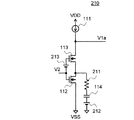
また、容量114は、図2に示すように、直列に抵抗211を備えても良い。この場合、容量114を経由する電流は、抵抗211による制限を受けるため、増幅回路210は帯域を制限する効果が期待でき、耐高周波ノイズ特性の良い増幅回路を実現できるメリットが見込める。
Further, the
また、容量114は接地端子に接続された構成としているが、図2に示すように、接地端子の電圧を基準とした電圧源212を備えても、同様の効果が得られる。例えば、電圧源212の電圧は電源端子の電圧と同じであってもよい。
Further, although the
また、NMOSトランジスタ113のゲートには、増幅回路の入力端子とNMOSトランジスタ113のゲートとの間に電圧源213を備えてもよい。即ち、NMOSトランジスタ113のソースは、増幅回路の入力電圧V2に電圧源213の電圧が加算された電圧に同期した電圧が現れるとしても、同様の効果が得られることは明らかである。また、電圧源213は、増幅回路の入力端子とNMOSトランジスタ112のゲートとの間に電圧源213を備えてもよい。
Further, the
また、以上の説明では、本実施形態の増幅回路は、NMOSトランジスタの使用を前提として説明したが、PMOSトランジスタの使用を前提とした増幅回路であっても、同様にして位相進み電流を生ずる容量による信号伝搬経路を設けることにより、位相特性を改善することが可能である。従って、この増幅回路を備えた負帰還増幅回路(例えば、ボルテージレギュレータ)は、発振に至る可能性を低下できるので、安定して動作することが可能となる。 In the above description, the amplifier circuit of the present embodiment has been described on the premise of using an NMOS transistor. It is possible to improve the phase characteristics by providing a signal propagation path. Therefore, a negative feedback amplifier circuit (for example, a voltage regulator) provided with this amplifier circuit can reduce the possibility of oscillation and can operate stably.
次に、図3に示す本実施形態の増幅回路を備えたボルテージレギュレータの実施形態について説明する。
ボルテージレギュレータ100は、図1に示した増幅回路110と、増幅回路120と、出力端子101と、を備える。増幅回路120は、NMOSトランジスタ121と、抵抗122と、抵抗123と、を備える。
Next, an embodiment of a voltage regulator provided with the amplifier circuit of this embodiment shown in FIG. 3 will be described.
The
増幅回路110は、出力端子が増幅回路120の入力端子に接続される。増幅回路120は、出力端子がボルテージレギュレータ100の出力端子101に接続され、帰還電圧出力端子が増幅回路110の入力端子に接続される。
The output terminal of the
NMOSトランジスタ121と抵抗122及び抵抗123は、電源端子と接地端子の間に直列に接続されている。NMOSトランジスタ121は、ゲートが増幅回路120の入力端子に接続され、ソースが増幅回路120の出力端子に接続される。抵抗122と抵抗123の接続点は、増幅回路120の帰還電圧出力端子に接続される。
The
次に、ボルテージレギュレータ100の動作について説明する。
増幅回路120は、入力された電圧V1aに基づいて増幅動作が成され、増幅した電圧VOUTを出力する。また、増幅回路120は、電圧VOUTを抵抗122及び抵抗123で分圧して帰還電圧である電圧V2を増幅回路110の入力端子に出力する。従って、増幅回路110と増幅回路120とは、互いに入力端子と出力端子とが接続されているため、負帰還増幅回路を構成している。電圧VOUTが低くなると、即ち帰還電圧である電圧V2が低くなると、増幅回路110は、NMOSトランジスタ112及び113がオフしていくので、出力する電圧V1aは高くなる。増幅回路120は、NMOSトランジスタ121がオンしていくので、出力する電圧VOUTは高くなる。また、電圧VOUTが高くなると、即ち帰還電圧である電圧V2が高くなると、増幅回路110は、NMOSトランジスタ112及び113をオンしていくので、出力する電圧V1aは低くなる。増幅回路120は、NMOSトランジスタ121がオフしていくので、出力する電圧VOUTは低くなる。即ち、ボルテージレギュレータ100は、電圧VOUTが一定に保たれるように動作する。
Next, the operation of the
The
増幅回路110は、図1の実施形態の説明において、帰還電圧の位相遅れの緩和が図られる効果について、明らかにした。従って、本実施形態の増幅回路110を備えた負帰還増幅回路であるボルテージレギュレータ100は、帰還電圧の位相が遅れの緩和が図られるから、安定して動作することが可能となる。
なお、ボルテージレギュレータ100は、増幅回路110を、上述したように、例えば増幅回路210のような回路構成としても、同様の効果が得られる。
In the description of the embodiment of FIG. 1, the
The
図4は、本実施形態の増幅回路を備えたボルテージレギュレータの他の例を示す回路である。
ボルテージレギュレータ200は、増幅回路110と、増幅回路130と、増幅回路140と、出力端子101と、を備える。
増幅回路130は、NMOSトランジスタ131と、抵抗132を備える。増幅回路140は、PMOSトランジスタ141と、抵抗142と、抵抗143と、を備える。
FIG. 4 is a circuit showing another example of a voltage regulator including the amplifier circuit of the present embodiment.
The
The
ボルテージレギュレータ200は、PMOSトランジスタ141による増幅回路140を備えたので、増幅回路110の出力する電圧V1aの増幅極性を反転させる増幅回路130を備えている。
このように構成したボルテージレギュレータ200は、ボルテージレギュレータ100と同様に負帰還増幅回路を構成するので、同様の効果が得られることは自明である。
Since the
Since the
以上説明したように、本実施形態の増幅回路によれば、位相特性を改善することが可能である。従って、この増幅回路を備えた負帰還増幅回路であるボルテージレギュレータは、帰還電圧の位相遅れの緩和が図られるため、発振に至る可能性を低下でき、即ち、安定して動作するボルテージレギュレータを提供することが可能となる。 As described above, according to the amplifier circuit of this embodiment, it is possible to improve the phase characteristics. Therefore, the voltage regulator, which is a negative feedback amplifier circuit including this amplifier circuit, can reduce the possibility of oscillation because the phase lag of the feedback voltage is mitigated, that is, provides a voltage regulator that operates stably. It becomes possible to do.
110、120、130、140 増幅回路
111 電流源
212、213 電圧源
110, 120, 130, 140
Claims (6)
電流源と、
ゲートが前記入力端子に接続される第1のトランジスタと、
ドレインが前記電流源に接続され、ソースが前記第1のトランジスタのドレインに接続され、ゲートが前記入力端子に接続される第2のトランジスタと、
一方の端子が前記第2のトランジスタのソースに接続された容量と、を備え、
前記第2のトランジスタのドレインが前記出力端子に接続されたことを特徴とする増幅回路。 An amplifying circuit that amplifies the voltage input to the input terminal and outputs it to the output terminal,
A current source;
A first transistor having a gate connected to the input terminal;
A second transistor having a drain connected to the current source, a source connected to the drain of the first transistor, and a gate connected to the input terminal;
A capacitor having one terminal connected to a source of the second transistor,
An amplifying circuit, wherein a drain of the second transistor is connected to the output terminal.
Priority Applications (5)
| Application Number | Priority Date | Filing Date | Title |
|---|---|---|---|
| JP2015242546A JP6632358B2 (en) | 2015-12-11 | 2015-12-11 | Amplifier and voltage regulator |
| TW105138742A TWI716500B (en) | 2015-12-11 | 2016-11-25 | Amplifier circuit and voltage regulator |
| KR1020160161377A KR102110110B1 (en) | 2015-12-11 | 2016-11-30 | Amplifier circuit and voltage regulator |
| US15/367,840 US9800156B2 (en) | 2015-12-11 | 2016-12-02 | Amplifier circuit and voltage regulator |
| CN201611119800.0A CN106896856B (en) | 2015-12-11 | 2016-12-08 | Amplifying circuit and voltage regulator |
Applications Claiming Priority (1)
| Application Number | Priority Date | Filing Date | Title |
|---|---|---|---|
| JP2015242546A JP6632358B2 (en) | 2015-12-11 | 2015-12-11 | Amplifier and voltage regulator |
Publications (2)
| Publication Number | Publication Date |
|---|---|
| JP2017108355A true JP2017108355A (en) | 2017-06-15 |
| JP6632358B2 JP6632358B2 (en) | 2020-01-22 |
Family
ID=59020177
Family Applications (1)
| Application Number | Title | Priority Date | Filing Date |
|---|---|---|---|
| JP2015242546A Active JP6632358B2 (en) | 2015-12-11 | 2015-12-11 | Amplifier and voltage regulator |
Country Status (5)
| Country | Link |
|---|---|
| US (1) | US9800156B2 (en) |
| JP (1) | JP6632358B2 (en) |
| KR (1) | KR102110110B1 (en) |
| CN (1) | CN106896856B (en) |
| TW (1) | TWI716500B (en) |
Families Citing this family (17)
| Publication number | Priority date | Publication date | Assignee | Title |
|---|---|---|---|---|
| WO2017196571A1 (en) * | 2016-05-07 | 2017-11-16 | Mark Telefus | High efficiency ac to dc converter and methods |
| US11056981B2 (en) | 2018-07-07 | 2021-07-06 | Intelesol, Llc | Method and apparatus for signal extraction with sample and hold and release |
| US11581725B2 (en) | 2018-07-07 | 2023-02-14 | Intelesol, Llc | Solid-state power interrupters |
| US11671029B2 (en) | 2018-07-07 | 2023-06-06 | Intelesol, Llc | AC to DC converters |
| TWI680366B (en) * | 2018-08-24 | 2019-12-21 | 新唐科技股份有限公司 | Regulator controlled by single transistor and integrated circuit using the same |
| US11334388B2 (en) | 2018-09-27 | 2022-05-17 | Amber Solutions, Inc. | Infrastructure support to enhance resource-constrained device capabilities |
| US11205011B2 (en) | 2018-09-27 | 2021-12-21 | Amber Solutions, Inc. | Privacy and the management of permissions |
| US11349296B2 (en) | 2018-10-01 | 2022-05-31 | Intelesol, Llc | Solid-state circuit interrupters |
| US10985548B2 (en) | 2018-10-01 | 2021-04-20 | Intelesol, Llc | Circuit interrupter with optical connection |
| CA3123586A1 (en) | 2018-12-17 | 2020-06-25 | Intelesol, Llc | Ac-driven light-emitting diode systems |
| US11373831B2 (en) | 2019-05-18 | 2022-06-28 | Amber Solutions, Inc. | Intelligent circuit breakers |
| EP4088125A4 (en) | 2020-01-21 | 2024-03-06 | Amber Semiconductor, Inc. | SMART CIRCUIT INTERRUPTION |
| EP4197086A4 (en) | 2020-08-11 | 2024-09-04 | Amber Semiconductor, Inc. | INTELLIGENT ENERGY SOURCE MONITORING AND SELECTION CONTROL SYSTEM |
| JP7504050B2 (en) * | 2021-03-25 | 2024-06-21 | エイブリック株式会社 | Shunt Regulator |
| US12113525B2 (en) | 2021-09-30 | 2024-10-08 | Amber Semiconductor, Inc. | Intelligent electrical switches |
| US12348028B2 (en) | 2021-10-22 | 2025-07-01 | Amber Semiconductor, Inc. | Multi-output programmable power manager |
| US12362646B2 (en) | 2022-01-26 | 2025-07-15 | Amber Semiconductor, Inc. | Controlling AC power to inductive loads |
Citations (7)
| Publication number | Priority date | Publication date | Assignee | Title |
|---|---|---|---|---|
| JPH03159405A (en) * | 1989-11-17 | 1991-07-09 | Sumitomo Electric Ind Ltd | amplifier circuit |
| JPH044768B2 (en) * | 1986-06-10 | 1992-01-29 | ||
| JPH05243861A (en) * | 1992-02-29 | 1993-09-21 | Sony Corp | Wide band amplifier circuit |
| JPH07183736A (en) * | 1993-12-22 | 1995-07-21 | Toshiba Corp | Electronic circuit |
| JPH11150427A (en) * | 1997-08-05 | 1999-06-02 | Toshiba Corp | Amplifier circuit and liquid crystal display device using the same |
| JP2014082535A (en) * | 2012-10-12 | 2014-05-08 | Asahi Kasei Electronics Co Ltd | Operational amplifier |
| JP2015159530A (en) * | 2014-01-21 | 2015-09-03 | セイコーインスツル株式会社 | Amplifier circuit |
Family Cites Families (14)
| Publication number | Priority date | Publication date | Assignee | Title |
|---|---|---|---|---|
| US4947063A (en) * | 1987-10-09 | 1990-08-07 | Western Digital Corporation | Method and apparatus for reducing transient noise in integrated circuits |
| FR2691306B1 (en) * | 1992-05-18 | 1994-08-12 | Sgs Thomson Microelectronics | Amplifier with output current limitation. |
| US5519357A (en) * | 1995-02-21 | 1996-05-21 | Apex Microtechnology | Biasing arrangement for a quasi-complementary output stage |
| US6278321B1 (en) * | 1999-10-21 | 2001-08-21 | Infineon Technologies Corporation | Method and apparatus for an improved variable gain amplifier |
| FR2911445B1 (en) * | 2007-01-16 | 2009-02-27 | Commissariat Energie Atomique | TRANSCONDUCTANCE AMPLIFIER WITH IMPROVED LINEARITY |
| US8072267B2 (en) * | 2009-06-09 | 2011-12-06 | Infineon Technologies Ag | Phase margin modification in operational transconductance amplifiers |
| TWI406120B (en) * | 2010-04-20 | 2013-08-21 | Novatek Microelectronics Corp | Spread spectrum circuit |
| JP5715401B2 (en) * | 2010-12-09 | 2015-05-07 | セイコーインスツル株式会社 | Voltage regulator |
| JP5715525B2 (en) * | 2011-08-05 | 2015-05-07 | セイコーインスツル株式会社 | Voltage regulator |
| US8912855B2 (en) * | 2012-02-08 | 2014-12-16 | Mediatek Inc. | Relaxation oscillator |
| TWI516020B (en) * | 2012-12-14 | 2016-01-01 | 敦泰電子股份有限公司 | Operational amplifying device with auto-adjustment output impedance |
| JP6342240B2 (en) * | 2013-08-26 | 2018-06-13 | エイブリック株式会社 | Voltage regulator |
| JP6316632B2 (en) * | 2014-03-25 | 2018-04-25 | エイブリック株式会社 | Voltage regulator |
| JP6457887B2 (en) * | 2015-05-21 | 2019-01-23 | エイブリック株式会社 | Voltage regulator |
-
2015
- 2015-12-11 JP JP2015242546A patent/JP6632358B2/en active Active
-
2016
- 2016-11-25 TW TW105138742A patent/TWI716500B/en active
- 2016-11-30 KR KR1020160161377A patent/KR102110110B1/en active Active
- 2016-12-02 US US15/367,840 patent/US9800156B2/en active Active
- 2016-12-08 CN CN201611119800.0A patent/CN106896856B/en active Active
Patent Citations (7)
| Publication number | Priority date | Publication date | Assignee | Title |
|---|---|---|---|---|
| JPH044768B2 (en) * | 1986-06-10 | 1992-01-29 | ||
| JPH03159405A (en) * | 1989-11-17 | 1991-07-09 | Sumitomo Electric Ind Ltd | amplifier circuit |
| JPH05243861A (en) * | 1992-02-29 | 1993-09-21 | Sony Corp | Wide band amplifier circuit |
| JPH07183736A (en) * | 1993-12-22 | 1995-07-21 | Toshiba Corp | Electronic circuit |
| JPH11150427A (en) * | 1997-08-05 | 1999-06-02 | Toshiba Corp | Amplifier circuit and liquid crystal display device using the same |
| JP2014082535A (en) * | 2012-10-12 | 2014-05-08 | Asahi Kasei Electronics Co Ltd | Operational amplifier |
| JP2015159530A (en) * | 2014-01-21 | 2015-09-03 | セイコーインスツル株式会社 | Amplifier circuit |
Also Published As
| Publication number | Publication date |
|---|---|
| US20170170730A1 (en) | 2017-06-15 |
| KR20170069923A (en) | 2017-06-21 |
| US9800156B2 (en) | 2017-10-24 |
| JP6632358B2 (en) | 2020-01-22 |
| KR102110110B1 (en) | 2020-05-13 |
| TW201722066A (en) | 2017-06-16 |
| CN106896856B (en) | 2020-07-07 |
| CN106896856A (en) | 2017-06-27 |
| TWI716500B (en) | 2021-01-21 |
Similar Documents
| Publication | Publication Date | Title |
|---|---|---|
| JP6632358B2 (en) | Amplifier and voltage regulator | |
| US20180292854A1 (en) | Voltage regulator | |
| JP2015100036A (en) | Buffer circuit | |
| JP4412507B2 (en) | Semiconductor circuit | |
| KR20120064617A (en) | Voltage regulator | |
| WO2014203703A1 (en) | Voltage regulator | |
| JP5883477B2 (en) | Voltage controlled oscillator | |
| US20130328629A1 (en) | Differential amplifier circuit | |
| JP6266333B2 (en) | Voltage regulator | |
| JP2014164702A (en) | Voltage regulator | |
| JP5833938B2 (en) | Voltage regulator | |
| US20070132494A1 (en) | Duty cycle correction amplification circuit | |
| US10574193B2 (en) | Class AB amplifier having cascode stage with filter for improving linearity | |
| US10187024B2 (en) | Input feed-forward technique for class AB amplifier | |
| JP4640788B2 (en) | Level conversion circuit | |
| JP5714958B2 (en) | Amplifier circuit | |
| KR101942160B1 (en) | The duty cycle corrector | |
| US9935619B2 (en) | Semiconductor device and communication module | |
| US9438215B2 (en) | Buffer circuit for buffering and settling input voltage to target voltage level and operation method thereof | |
| JP2010109710A (en) | Variable gain amplifier | |
| WO2013186863A1 (en) | Amplification circuit | |
| JP2015019328A (en) | Amplification circuit | |
| JP5355648B2 (en) | High frequency amplifier | |
| JP2014168225A (en) | High frequency amplifier | |
| JP2012151748A (en) | Power amplification synthesis circuit, and power amplification circuit, transmission device, and communication device using the same |
Legal Events
| Date | Code | Title | Description |
|---|---|---|---|
| A711 | Notification of change in applicant |
Free format text: JAPANESE INTERMEDIATE CODE: A711 Effective date: 20160112 |
|
| A621 | Written request for application examination |
Free format text: JAPANESE INTERMEDIATE CODE: A621 Effective date: 20181004 |
|
| A977 | Report on retrieval |
Free format text: JAPANESE INTERMEDIATE CODE: A971007 Effective date: 20190606 |
|
| A131 | Notification of reasons for refusal |
Free format text: JAPANESE INTERMEDIATE CODE: A131 Effective date: 20190618 |
|
| A521 | Request for written amendment filed |
Free format text: JAPANESE INTERMEDIATE CODE: A523 Effective date: 20190717 |
|
| TRDD | Decision of grant or rejection written | ||
| A01 | Written decision to grant a patent or to grant a registration (utility model) |
Free format text: JAPANESE INTERMEDIATE CODE: A01 Effective date: 20191210 |
|
| A61 | First payment of annual fees (during grant procedure) |
Free format text: JAPANESE INTERMEDIATE CODE: A61 Effective date: 20191210 |
|
| R150 | Certificate of patent or registration of utility model |
Ref document number: 6632358 Country of ref document: JP Free format text: JAPANESE INTERMEDIATE CODE: R150 |
|
| S531 | Written request for registration of change of domicile |
Free format text: JAPANESE INTERMEDIATE CODE: R313531 |
|
| R350 | Written notification of registration of transfer |
Free format text: JAPANESE INTERMEDIATE CODE: R350 |
|
| R250 | Receipt of annual fees |
Free format text: JAPANESE INTERMEDIATE CODE: R250 |
|
| S531 | Written request for registration of change of domicile |
Free format text: JAPANESE INTERMEDIATE CODE: R313531 |
|
| R350 | Written notification of registration of transfer |
Free format text: JAPANESE INTERMEDIATE CODE: R350 |
|
| R250 | Receipt of annual fees |
Free format text: JAPANESE INTERMEDIATE CODE: R250 |
|
| R250 | Receipt of annual fees |
Free format text: JAPANESE INTERMEDIATE CODE: R250 |
|
| R250 | Receipt of annual fees |
Free format text: JAPANESE INTERMEDIATE CODE: R250 |