JP2017111438A - 表示装置及び分離方法 - Google Patents
表示装置及び分離方法 Download PDFInfo
- Publication number
- JP2017111438A JP2017111438A JP2016236993A JP2016236993A JP2017111438A JP 2017111438 A JP2017111438 A JP 2017111438A JP 2016236993 A JP2016236993 A JP 2016236993A JP 2016236993 A JP2016236993 A JP 2016236993A JP 2017111438 A JP2017111438 A JP 2017111438A
- Authority
- JP
- Japan
- Prior art keywords
- layer
- insulating layer
- oxide
- transistor
- display device
- Prior art date
- Legal status (The legal status is an assumption and is not a legal conclusion. Google has not performed a legal analysis and makes no representation as to the accuracy of the status listed.)
- Granted
Links
Images

















Classifications
-
- G—PHYSICS
- G02—OPTICS
- G02F—OPTICAL DEVICES OR ARRANGEMENTS FOR THE CONTROL OF LIGHT BY MODIFICATION OF THE OPTICAL PROPERTIES OF THE MEDIA OF THE ELEMENTS INVOLVED THEREIN; NON-LINEAR OPTICS; FREQUENCY-CHANGING OF LIGHT; OPTICAL LOGIC ELEMENTS; OPTICAL ANALOGUE/DIGITAL CONVERTERS
- G02F1/00—Devices or arrangements for the control of the intensity, colour, phase, polarisation or direction of light arriving from an independent light source, e.g. switching, gating or modulating; Non-linear optics
- G02F1/01—Devices or arrangements for the control of the intensity, colour, phase, polarisation or direction of light arriving from an independent light source, e.g. switching, gating or modulating; Non-linear optics for the control of the intensity, phase, polarisation or colour
- G02F1/13—Devices or arrangements for the control of the intensity, colour, phase, polarisation or direction of light arriving from an independent light source, e.g. switching, gating or modulating; Non-linear optics for the control of the intensity, phase, polarisation or colour based on liquid crystals, e.g. single liquid crystal display cells
- G02F1/133—Constructional arrangements; Operation of liquid crystal cells; Circuit arrangements
- G02F1/136—Liquid crystal cells structurally associated with a semi-conducting layer or substrate, e.g. cells forming part of an integrated circuit
- G02F1/1362—Active matrix addressed cells
- G02F1/1368—Active matrix addressed cells in which the switching element is a three-electrode device
-
- G—PHYSICS
- G02—OPTICS
- G02F—OPTICAL DEVICES OR ARRANGEMENTS FOR THE CONTROL OF LIGHT BY MODIFICATION OF THE OPTICAL PROPERTIES OF THE MEDIA OF THE ELEMENTS INVOLVED THEREIN; NON-LINEAR OPTICS; FREQUENCY-CHANGING OF LIGHT; OPTICAL LOGIC ELEMENTS; OPTICAL ANALOGUE/DIGITAL CONVERTERS
- G02F1/00—Devices or arrangements for the control of the intensity, colour, phase, polarisation or direction of light arriving from an independent light source, e.g. switching, gating or modulating; Non-linear optics
- G02F1/01—Devices or arrangements for the control of the intensity, colour, phase, polarisation or direction of light arriving from an independent light source, e.g. switching, gating or modulating; Non-linear optics for the control of the intensity, phase, polarisation or colour
- G02F1/13—Devices or arrangements for the control of the intensity, colour, phase, polarisation or direction of light arriving from an independent light source, e.g. switching, gating or modulating; Non-linear optics for the control of the intensity, phase, polarisation or colour based on liquid crystals, e.g. single liquid crystal display cells
- G02F1/133—Constructional arrangements; Operation of liquid crystal cells; Circuit arrangements
- G02F1/1333—Constructional arrangements; Manufacturing methods
- G02F1/133345—Insulating layers
-
- G—PHYSICS
- G02—OPTICS
- G02F—OPTICAL DEVICES OR ARRANGEMENTS FOR THE CONTROL OF LIGHT BY MODIFICATION OF THE OPTICAL PROPERTIES OF THE MEDIA OF THE ELEMENTS INVOLVED THEREIN; NON-LINEAR OPTICS; FREQUENCY-CHANGING OF LIGHT; OPTICAL LOGIC ELEMENTS; OPTICAL ANALOGUE/DIGITAL CONVERTERS
- G02F1/00—Devices or arrangements for the control of the intensity, colour, phase, polarisation or direction of light arriving from an independent light source, e.g. switching, gating or modulating; Non-linear optics
- G02F1/01—Devices or arrangements for the control of the intensity, colour, phase, polarisation or direction of light arriving from an independent light source, e.g. switching, gating or modulating; Non-linear optics for the control of the intensity, phase, polarisation or colour
- G02F1/13—Devices or arrangements for the control of the intensity, colour, phase, polarisation or direction of light arriving from an independent light source, e.g. switching, gating or modulating; Non-linear optics for the control of the intensity, phase, polarisation or colour based on liquid crystals, e.g. single liquid crystal display cells
- G02F1/133—Constructional arrangements; Operation of liquid crystal cells; Circuit arrangements
- G02F1/1333—Constructional arrangements; Manufacturing methods
- G02F1/133351—Manufacturing of individual cells out of a plurality of cells, e.g. by dicing
-
- G—PHYSICS
- G02—OPTICS
- G02F—OPTICAL DEVICES OR ARRANGEMENTS FOR THE CONTROL OF LIGHT BY MODIFICATION OF THE OPTICAL PROPERTIES OF THE MEDIA OF THE ELEMENTS INVOLVED THEREIN; NON-LINEAR OPTICS; FREQUENCY-CHANGING OF LIGHT; OPTICAL LOGIC ELEMENTS; OPTICAL ANALOGUE/DIGITAL CONVERTERS
- G02F1/00—Devices or arrangements for the control of the intensity, colour, phase, polarisation or direction of light arriving from an independent light source, e.g. switching, gating or modulating; Non-linear optics
- G02F1/01—Devices or arrangements for the control of the intensity, colour, phase, polarisation or direction of light arriving from an independent light source, e.g. switching, gating or modulating; Non-linear optics for the control of the intensity, phase, polarisation or colour
- G02F1/13—Devices or arrangements for the control of the intensity, colour, phase, polarisation or direction of light arriving from an independent light source, e.g. switching, gating or modulating; Non-linear optics for the control of the intensity, phase, polarisation or colour based on liquid crystals, e.g. single liquid crystal display cells
- G02F1/133—Constructional arrangements; Operation of liquid crystal cells; Circuit arrangements
- G02F1/1333—Constructional arrangements; Manufacturing methods
- G02F1/13338—Input devices, e.g. touch panels
-
- G—PHYSICS
- G02—OPTICS
- G02F—OPTICAL DEVICES OR ARRANGEMENTS FOR THE CONTROL OF LIGHT BY MODIFICATION OF THE OPTICAL PROPERTIES OF THE MEDIA OF THE ELEMENTS INVOLVED THEREIN; NON-LINEAR OPTICS; FREQUENCY-CHANGING OF LIGHT; OPTICAL LOGIC ELEMENTS; OPTICAL ANALOGUE/DIGITAL CONVERTERS
- G02F1/00—Devices or arrangements for the control of the intensity, colour, phase, polarisation or direction of light arriving from an independent light source, e.g. switching, gating or modulating; Non-linear optics
- G02F1/01—Devices or arrangements for the control of the intensity, colour, phase, polarisation or direction of light arriving from an independent light source, e.g. switching, gating or modulating; Non-linear optics for the control of the intensity, phase, polarisation or colour
- G02F1/13—Devices or arrangements for the control of the intensity, colour, phase, polarisation or direction of light arriving from an independent light source, e.g. switching, gating or modulating; Non-linear optics for the control of the intensity, phase, polarisation or colour based on liquid crystals, e.g. single liquid crystal display cells
- G02F1/133—Constructional arrangements; Operation of liquid crystal cells; Circuit arrangements
- G02F1/1333—Constructional arrangements; Manufacturing methods
- G02F1/1337—Surface-induced orientation of the liquid crystal molecules, e.g. by alignment layers
- G02F1/133742—Surface-induced orientation of the liquid crystal molecules, e.g. by alignment layers for homeotropic alignment
-
- G—PHYSICS
- G02—OPTICS
- G02F—OPTICAL DEVICES OR ARRANGEMENTS FOR THE CONTROL OF LIGHT BY MODIFICATION OF THE OPTICAL PROPERTIES OF THE MEDIA OF THE ELEMENTS INVOLVED THEREIN; NON-LINEAR OPTICS; FREQUENCY-CHANGING OF LIGHT; OPTICAL LOGIC ELEMENTS; OPTICAL ANALOGUE/DIGITAL CONVERTERS
- G02F1/00—Devices or arrangements for the control of the intensity, colour, phase, polarisation or direction of light arriving from an independent light source, e.g. switching, gating or modulating; Non-linear optics
- G02F1/01—Devices or arrangements for the control of the intensity, colour, phase, polarisation or direction of light arriving from an independent light source, e.g. switching, gating or modulating; Non-linear optics for the control of the intensity, phase, polarisation or colour
- G02F1/13—Devices or arrangements for the control of the intensity, colour, phase, polarisation or direction of light arriving from an independent light source, e.g. switching, gating or modulating; Non-linear optics for the control of the intensity, phase, polarisation or colour based on liquid crystals, e.g. single liquid crystal display cells
- G02F1/133—Constructional arrangements; Operation of liquid crystal cells; Circuit arrangements
- G02F1/1333—Constructional arrangements; Manufacturing methods
- G02F1/1343—Electrodes
- G02F1/134309—Electrodes characterised by their geometrical arrangement
-
- G—PHYSICS
- G02—OPTICS
- G02F—OPTICAL DEVICES OR ARRANGEMENTS FOR THE CONTROL OF LIGHT BY MODIFICATION OF THE OPTICAL PROPERTIES OF THE MEDIA OF THE ELEMENTS INVOLVED THEREIN; NON-LINEAR OPTICS; FREQUENCY-CHANGING OF LIGHT; OPTICAL LOGIC ELEMENTS; OPTICAL ANALOGUE/DIGITAL CONVERTERS
- G02F1/00—Devices or arrangements for the control of the intensity, colour, phase, polarisation or direction of light arriving from an independent light source, e.g. switching, gating or modulating; Non-linear optics
- G02F1/01—Devices or arrangements for the control of the intensity, colour, phase, polarisation or direction of light arriving from an independent light source, e.g. switching, gating or modulating; Non-linear optics for the control of the intensity, phase, polarisation or colour
- G02F1/13—Devices or arrangements for the control of the intensity, colour, phase, polarisation or direction of light arriving from an independent light source, e.g. switching, gating or modulating; Non-linear optics for the control of the intensity, phase, polarisation or colour based on liquid crystals, e.g. single liquid crystal display cells
- G02F1/133—Constructional arrangements; Operation of liquid crystal cells; Circuit arrangements
- G02F1/1333—Constructional arrangements; Manufacturing methods
- G02F1/1343—Electrodes
- G02F1/13439—Electrodes characterised by their electrical, optical, physical properties; materials therefor; method of making
-
- G—PHYSICS
- G02—OPTICS
- G02F—OPTICAL DEVICES OR ARRANGEMENTS FOR THE CONTROL OF LIGHT BY MODIFICATION OF THE OPTICAL PROPERTIES OF THE MEDIA OF THE ELEMENTS INVOLVED THEREIN; NON-LINEAR OPTICS; FREQUENCY-CHANGING OF LIGHT; OPTICAL LOGIC ELEMENTS; OPTICAL ANALOGUE/DIGITAL CONVERTERS
- G02F1/00—Devices or arrangements for the control of the intensity, colour, phase, polarisation or direction of light arriving from an independent light source, e.g. switching, gating or modulating; Non-linear optics
- G02F1/01—Devices or arrangements for the control of the intensity, colour, phase, polarisation or direction of light arriving from an independent light source, e.g. switching, gating or modulating; Non-linear optics for the control of the intensity, phase, polarisation or colour
- G02F1/13—Devices or arrangements for the control of the intensity, colour, phase, polarisation or direction of light arriving from an independent light source, e.g. switching, gating or modulating; Non-linear optics for the control of the intensity, phase, polarisation or colour based on liquid crystals, e.g. single liquid crystal display cells
- G02F1/133—Constructional arrangements; Operation of liquid crystal cells; Circuit arrangements
- G02F1/136—Liquid crystal cells structurally associated with a semi-conducting layer or substrate, e.g. cells forming part of an integrated circuit
- G02F1/1362—Active matrix addressed cells
- G02F1/136286—Wiring, e.g. gate line, drain line
-
- G—PHYSICS
- G06—COMPUTING OR CALCULATING; COUNTING
- G06F—ELECTRIC DIGITAL DATA PROCESSING
- G06F3/00—Input arrangements for transferring data to be processed into a form capable of being handled by the computer; Output arrangements for transferring data from processing unit to output unit, e.g. interface arrangements
- G06F3/01—Input arrangements or combined input and output arrangements for interaction between user and computer
- G06F3/03—Arrangements for converting the position or the displacement of a member into a coded form
- G06F3/041—Digitisers, e.g. for touch screens or touch pads, characterised by the transducing means
- G06F3/0412—Digitisers structurally integrated in a display
-
- G—PHYSICS
- G06—COMPUTING OR CALCULATING; COUNTING
- G06F—ELECTRIC DIGITAL DATA PROCESSING
- G06F3/00—Input arrangements for transferring data to be processed into a form capable of being handled by the computer; Output arrangements for transferring data from processing unit to output unit, e.g. interface arrangements
- G06F3/01—Input arrangements or combined input and output arrangements for interaction between user and computer
- G06F3/03—Arrangements for converting the position or the displacement of a member into a coded form
- G06F3/041—Digitisers, e.g. for touch screens or touch pads, characterised by the transducing means
- G06F3/044—Digitisers, e.g. for touch screens or touch pads, characterised by the transducing means by capacitive means
-
- G—PHYSICS
- G06—COMPUTING OR CALCULATING; COUNTING
- G06F—ELECTRIC DIGITAL DATA PROCESSING
- G06F3/00—Input arrangements for transferring data to be processed into a form capable of being handled by the computer; Output arrangements for transferring data from processing unit to output unit, e.g. interface arrangements
- G06F3/01—Input arrangements or combined input and output arrangements for interaction between user and computer
- G06F3/03—Arrangements for converting the position or the displacement of a member into a coded form
- G06F3/041—Digitisers, e.g. for touch screens or touch pads, characterised by the transducing means
- G06F3/044—Digitisers, e.g. for touch screens or touch pads, characterised by the transducing means by capacitive means
- G06F3/0446—Digitisers, e.g. for touch screens or touch pads, characterised by the transducing means by capacitive means using a grid-like structure of electrodes in at least two directions, e.g. using row and column electrodes
-
- G—PHYSICS
- G09—EDUCATION; CRYPTOGRAPHY; DISPLAY; ADVERTISING; SEALS
- G09G—ARRANGEMENTS OR CIRCUITS FOR CONTROL OF INDICATING DEVICES USING STATIC MEANS TO PRESENT VARIABLE INFORMATION
- G09G3/00—Control arrangements or circuits, of interest only in connection with visual indicators other than cathode-ray tubes
- G09G3/20—Control arrangements or circuits, of interest only in connection with visual indicators other than cathode-ray tubes for presentation of an assembly of a number of characters, e.g. a page, by composing the assembly by combination of individual elements arranged in a matrix no fixed position being assigned to or needed to be assigned to the individual characters or partial characters
- G09G3/34—Control arrangements or circuits, of interest only in connection with visual indicators other than cathode-ray tubes for presentation of an assembly of a number of characters, e.g. a page, by composing the assembly by combination of individual elements arranged in a matrix no fixed position being assigned to or needed to be assigned to the individual characters or partial characters by control of light from an independent source
- G09G3/36—Control arrangements or circuits, of interest only in connection with visual indicators other than cathode-ray tubes for presentation of an assembly of a number of characters, e.g. a page, by composing the assembly by combination of individual elements arranged in a matrix no fixed position being assigned to or needed to be assigned to the individual characters or partial characters by control of light from an independent source using liquid crystals
- G09G3/3611—Control of matrices with row and column drivers
- G09G3/3648—Control of matrices with row and column drivers using an active matrix
-
- H—ELECTRICITY
- H10—SEMICONDUCTOR DEVICES; ELECTRIC SOLID-STATE DEVICES NOT OTHERWISE PROVIDED FOR
- H10D—INORGANIC ELECTRIC SEMICONDUCTOR DEVICES
- H10D30/00—Field-effect transistors [FET]
- H10D30/60—Insulated-gate field-effect transistors [IGFET]
- H10D30/67—Thin-film transistors [TFT]
- H10D30/6729—Thin-film transistors [TFT] characterised by the electrodes
- H10D30/673—Thin-film transistors [TFT] characterised by the electrodes characterised by the shapes, relative sizes or dispositions of the gate electrodes
- H10D30/6733—Multi-gate TFTs
- H10D30/6734—Multi-gate TFTs having gate electrodes arranged on both top and bottom sides of the channel, e.g. dual-gate TFTs
-
- H—ELECTRICITY
- H10—SEMICONDUCTOR DEVICES; ELECTRIC SOLID-STATE DEVICES NOT OTHERWISE PROVIDED FOR
- H10D—INORGANIC ELECTRIC SEMICONDUCTOR DEVICES
- H10D30/00—Field-effect transistors [FET]
- H10D30/60—Insulated-gate field-effect transistors [IGFET]
- H10D30/67—Thin-film transistors [TFT]
- H10D30/674—Thin-film transistors [TFT] characterised by the active materials
- H10D30/6755—Oxide semiconductors, e.g. zinc oxide, copper aluminium oxide or cadmium stannate
-
- H—ELECTRICITY
- H10—SEMICONDUCTOR DEVICES; ELECTRIC SOLID-STATE DEVICES NOT OTHERWISE PROVIDED FOR
- H10D—INORGANIC ELECTRIC SEMICONDUCTOR DEVICES
- H10D30/00—Field-effect transistors [FET]
- H10D30/60—Insulated-gate field-effect transistors [IGFET]
- H10D30/67—Thin-film transistors [TFT]
- H10D30/6757—Thin-film transistors [TFT] characterised by the structure of the channel, e.g. transverse or longitudinal shape or doping profile
-
- H—ELECTRICITY
- H10—SEMICONDUCTOR DEVICES; ELECTRIC SOLID-STATE DEVICES NOT OTHERWISE PROVIDED FOR
- H10D—INORGANIC ELECTRIC SEMICONDUCTOR DEVICES
- H10D62/00—Semiconductor bodies, or regions thereof, of devices having potential barriers
- H10D62/40—Crystalline structures
- H10D62/405—Orientations of crystalline planes
-
- H—ELECTRICITY
- H10—SEMICONDUCTOR DEVICES; ELECTRIC SOLID-STATE DEVICES NOT OTHERWISE PROVIDED FOR
- H10D—INORGANIC ELECTRIC SEMICONDUCTOR DEVICES
- H10D62/00—Semiconductor bodies, or regions thereof, of devices having potential barriers
- H10D62/80—Semiconductor bodies, or regions thereof, of devices having potential barriers characterised by the materials
-
- H—ELECTRICITY
- H10—SEMICONDUCTOR DEVICES; ELECTRIC SOLID-STATE DEVICES NOT OTHERWISE PROVIDED FOR
- H10D—INORGANIC ELECTRIC SEMICONDUCTOR DEVICES
- H10D86/00—Integrated devices formed in or on insulating or conducting substrates, e.g. formed in silicon-on-insulator [SOI] substrates or on stainless steel or glass substrates
- H10D86/01—Manufacture or treatment
- H10D86/021—Manufacture or treatment of multiple TFTs
-
- H—ELECTRICITY
- H10—SEMICONDUCTOR DEVICES; ELECTRIC SOLID-STATE DEVICES NOT OTHERWISE PROVIDED FOR
- H10D—INORGANIC ELECTRIC SEMICONDUCTOR DEVICES
- H10D86/00—Integrated devices formed in or on insulating or conducting substrates, e.g. formed in silicon-on-insulator [SOI] substrates or on stainless steel or glass substrates
- H10D86/01—Manufacture or treatment
- H10D86/021—Manufacture or treatment of multiple TFTs
- H10D86/0214—Manufacture or treatment of multiple TFTs using temporary substrates
-
- H—ELECTRICITY
- H10—SEMICONDUCTOR DEVICES; ELECTRIC SOLID-STATE DEVICES NOT OTHERWISE PROVIDED FOR
- H10D—INORGANIC ELECTRIC SEMICONDUCTOR DEVICES
- H10D86/00—Integrated devices formed in or on insulating or conducting substrates, e.g. formed in silicon-on-insulator [SOI] substrates or on stainless steel or glass substrates
- H10D86/40—Integrated devices formed in or on insulating or conducting substrates, e.g. formed in silicon-on-insulator [SOI] substrates or on stainless steel or glass substrates characterised by multiple TFTs
- H10D86/421—Integrated devices formed in or on insulating or conducting substrates, e.g. formed in silicon-on-insulator [SOI] substrates or on stainless steel or glass substrates characterised by multiple TFTs having a particular composition, shape or crystalline structure of the active layer
- H10D86/423—Integrated devices formed in or on insulating or conducting substrates, e.g. formed in silicon-on-insulator [SOI] substrates or on stainless steel or glass substrates characterised by multiple TFTs having a particular composition, shape or crystalline structure of the active layer comprising semiconductor materials not belonging to the Group IV, e.g. InGaZnO
-
- H—ELECTRICITY
- H10—SEMICONDUCTOR DEVICES; ELECTRIC SOLID-STATE DEVICES NOT OTHERWISE PROVIDED FOR
- H10D—INORGANIC ELECTRIC SEMICONDUCTOR DEVICES
- H10D86/00—Integrated devices formed in or on insulating or conducting substrates, e.g. formed in silicon-on-insulator [SOI] substrates or on stainless steel or glass substrates
- H10D86/40—Integrated devices formed in or on insulating or conducting substrates, e.g. formed in silicon-on-insulator [SOI] substrates or on stainless steel or glass substrates characterised by multiple TFTs
- H10D86/441—Interconnections, e.g. scanning lines
-
- H—ELECTRICITY
- H10—SEMICONDUCTOR DEVICES; ELECTRIC SOLID-STATE DEVICES NOT OTHERWISE PROVIDED FOR
- H10D—INORGANIC ELECTRIC SEMICONDUCTOR DEVICES
- H10D86/00—Integrated devices formed in or on insulating or conducting substrates, e.g. formed in silicon-on-insulator [SOI] substrates or on stainless steel or glass substrates
- H10D86/40—Integrated devices formed in or on insulating or conducting substrates, e.g. formed in silicon-on-insulator [SOI] substrates or on stainless steel or glass substrates characterised by multiple TFTs
- H10D86/60—Integrated devices formed in or on insulating or conducting substrates, e.g. formed in silicon-on-insulator [SOI] substrates or on stainless steel or glass substrates characterised by multiple TFTs wherein the TFTs are in active matrices
-
- G—PHYSICS
- G02—OPTICS
- G02F—OPTICAL DEVICES OR ARRANGEMENTS FOR THE CONTROL OF LIGHT BY MODIFICATION OF THE OPTICAL PROPERTIES OF THE MEDIA OF THE ELEMENTS INVOLVED THEREIN; NON-LINEAR OPTICS; FREQUENCY-CHANGING OF LIGHT; OPTICAL LOGIC ELEMENTS; OPTICAL ANALOGUE/DIGITAL CONVERTERS
- G02F1/00—Devices or arrangements for the control of the intensity, colour, phase, polarisation or direction of light arriving from an independent light source, e.g. switching, gating or modulating; Non-linear optics
- G02F1/01—Devices or arrangements for the control of the intensity, colour, phase, polarisation or direction of light arriving from an independent light source, e.g. switching, gating or modulating; Non-linear optics for the control of the intensity, phase, polarisation or colour
- G02F1/13—Devices or arrangements for the control of the intensity, colour, phase, polarisation or direction of light arriving from an independent light source, e.g. switching, gating or modulating; Non-linear optics for the control of the intensity, phase, polarisation or colour based on liquid crystals, e.g. single liquid crystal display cells
- G02F1/133—Constructional arrangements; Operation of liquid crystal cells; Circuit arrangements
- G02F1/1333—Constructional arrangements; Manufacturing methods
- G02F1/1335—Structural association of cells with optical devices, e.g. polarisers or reflectors
- G02F1/133509—Filters, e.g. light shielding masks
- G02F1/133512—Light shielding layers, e.g. black matrix
-
- G—PHYSICS
- G02—OPTICS
- G02F—OPTICAL DEVICES OR ARRANGEMENTS FOR THE CONTROL OF LIGHT BY MODIFICATION OF THE OPTICAL PROPERTIES OF THE MEDIA OF THE ELEMENTS INVOLVED THEREIN; NON-LINEAR OPTICS; FREQUENCY-CHANGING OF LIGHT; OPTICAL LOGIC ELEMENTS; OPTICAL ANALOGUE/DIGITAL CONVERTERS
- G02F1/00—Devices or arrangements for the control of the intensity, colour, phase, polarisation or direction of light arriving from an independent light source, e.g. switching, gating or modulating; Non-linear optics
- G02F1/01—Devices or arrangements for the control of the intensity, colour, phase, polarisation or direction of light arriving from an independent light source, e.g. switching, gating or modulating; Non-linear optics for the control of the intensity, phase, polarisation or colour
- G02F1/13—Devices or arrangements for the control of the intensity, colour, phase, polarisation or direction of light arriving from an independent light source, e.g. switching, gating or modulating; Non-linear optics for the control of the intensity, phase, polarisation or colour based on liquid crystals, e.g. single liquid crystal display cells
- G02F1/133—Constructional arrangements; Operation of liquid crystal cells; Circuit arrangements
- G02F1/1333—Constructional arrangements; Manufacturing methods
- G02F1/1335—Structural association of cells with optical devices, e.g. polarisers or reflectors
- G02F1/133528—Polarisers
-
- G—PHYSICS
- G02—OPTICS
- G02F—OPTICAL DEVICES OR ARRANGEMENTS FOR THE CONTROL OF LIGHT BY MODIFICATION OF THE OPTICAL PROPERTIES OF THE MEDIA OF THE ELEMENTS INVOLVED THEREIN; NON-LINEAR OPTICS; FREQUENCY-CHANGING OF LIGHT; OPTICAL LOGIC ELEMENTS; OPTICAL ANALOGUE/DIGITAL CONVERTERS
- G02F1/00—Devices or arrangements for the control of the intensity, colour, phase, polarisation or direction of light arriving from an independent light source, e.g. switching, gating or modulating; Non-linear optics
- G02F1/01—Devices or arrangements for the control of the intensity, colour, phase, polarisation or direction of light arriving from an independent light source, e.g. switching, gating or modulating; Non-linear optics for the control of the intensity, phase, polarisation or colour
- G02F1/13—Devices or arrangements for the control of the intensity, colour, phase, polarisation or direction of light arriving from an independent light source, e.g. switching, gating or modulating; Non-linear optics for the control of the intensity, phase, polarisation or colour based on liquid crystals, e.g. single liquid crystal display cells
- G02F1/133—Constructional arrangements; Operation of liquid crystal cells; Circuit arrangements
- G02F1/1333—Constructional arrangements; Manufacturing methods
- G02F1/1337—Surface-induced orientation of the liquid crystal molecules, e.g. by alignment layers
-
- G—PHYSICS
- G02—OPTICS
- G02F—OPTICAL DEVICES OR ARRANGEMENTS FOR THE CONTROL OF LIGHT BY MODIFICATION OF THE OPTICAL PROPERTIES OF THE MEDIA OF THE ELEMENTS INVOLVED THEREIN; NON-LINEAR OPTICS; FREQUENCY-CHANGING OF LIGHT; OPTICAL LOGIC ELEMENTS; OPTICAL ANALOGUE/DIGITAL CONVERTERS
- G02F1/00—Devices or arrangements for the control of the intensity, colour, phase, polarisation or direction of light arriving from an independent light source, e.g. switching, gating or modulating; Non-linear optics
- G02F1/01—Devices or arrangements for the control of the intensity, colour, phase, polarisation or direction of light arriving from an independent light source, e.g. switching, gating or modulating; Non-linear optics for the control of the intensity, phase, polarisation or colour
- G02F1/13—Devices or arrangements for the control of the intensity, colour, phase, polarisation or direction of light arriving from an independent light source, e.g. switching, gating or modulating; Non-linear optics for the control of the intensity, phase, polarisation or colour based on liquid crystals, e.g. single liquid crystal display cells
- G02F1/133—Constructional arrangements; Operation of liquid crystal cells; Circuit arrangements
- G02F1/1333—Constructional arrangements; Manufacturing methods
- G02F1/1343—Electrodes
- G02F1/134309—Electrodes characterised by their geometrical arrangement
- G02F1/134318—Electrodes characterised by their geometrical arrangement having a patterned common electrode
-
- G—PHYSICS
- G02—OPTICS
- G02F—OPTICAL DEVICES OR ARRANGEMENTS FOR THE CONTROL OF LIGHT BY MODIFICATION OF THE OPTICAL PROPERTIES OF THE MEDIA OF THE ELEMENTS INVOLVED THEREIN; NON-LINEAR OPTICS; FREQUENCY-CHANGING OF LIGHT; OPTICAL LOGIC ELEMENTS; OPTICAL ANALOGUE/DIGITAL CONVERTERS
- G02F2201/00—Constructional arrangements not provided for in groups G02F1/00 - G02F7/00
- G02F2201/12—Constructional arrangements not provided for in groups G02F1/00 - G02F7/00 electrode
- G02F2201/121—Constructional arrangements not provided for in groups G02F1/00 - G02F7/00 electrode common or background
-
- G—PHYSICS
- G02—OPTICS
- G02F—OPTICAL DEVICES OR ARRANGEMENTS FOR THE CONTROL OF LIGHT BY MODIFICATION OF THE OPTICAL PROPERTIES OF THE MEDIA OF THE ELEMENTS INVOLVED THEREIN; NON-LINEAR OPTICS; FREQUENCY-CHANGING OF LIGHT; OPTICAL LOGIC ELEMENTS; OPTICAL ANALOGUE/DIGITAL CONVERTERS
- G02F2201/00—Constructional arrangements not provided for in groups G02F1/00 - G02F7/00
- G02F2201/12—Constructional arrangements not provided for in groups G02F1/00 - G02F7/00 electrode
- G02F2201/123—Constructional arrangements not provided for in groups G02F1/00 - G02F7/00 electrode pixel
-
- G—PHYSICS
- G02—OPTICS
- G02F—OPTICAL DEVICES OR ARRANGEMENTS FOR THE CONTROL OF LIGHT BY MODIFICATION OF THE OPTICAL PROPERTIES OF THE MEDIA OF THE ELEMENTS INVOLVED THEREIN; NON-LINEAR OPTICS; FREQUENCY-CHANGING OF LIGHT; OPTICAL LOGIC ELEMENTS; OPTICAL ANALOGUE/DIGITAL CONVERTERS
- G02F2201/00—Constructional arrangements not provided for in groups G02F1/00 - G02F7/00
- G02F2201/40—Arrangements for improving the aperture ratio
-
- G—PHYSICS
- G02—OPTICS
- G02F—OPTICAL DEVICES OR ARRANGEMENTS FOR THE CONTROL OF LIGHT BY MODIFICATION OF THE OPTICAL PROPERTIES OF THE MEDIA OF THE ELEMENTS INVOLVED THEREIN; NON-LINEAR OPTICS; FREQUENCY-CHANGING OF LIGHT; OPTICAL LOGIC ELEMENTS; OPTICAL ANALOGUE/DIGITAL CONVERTERS
- G02F2201/00—Constructional arrangements not provided for in groups G02F1/00 - G02F7/00
- G02F2201/48—Flattening arrangements
-
- G—PHYSICS
- G02—OPTICS
- G02F—OPTICAL DEVICES OR ARRANGEMENTS FOR THE CONTROL OF LIGHT BY MODIFICATION OF THE OPTICAL PROPERTIES OF THE MEDIA OF THE ELEMENTS INVOLVED THEREIN; NON-LINEAR OPTICS; FREQUENCY-CHANGING OF LIGHT; OPTICAL LOGIC ELEMENTS; OPTICAL ANALOGUE/DIGITAL CONVERTERS
- G02F2202/00—Materials and properties
- G02F2202/10—Materials and properties semiconductor
-
- G—PHYSICS
- G02—OPTICS
- G02F—OPTICAL DEVICES OR ARRANGEMENTS FOR THE CONTROL OF LIGHT BY MODIFICATION OF THE OPTICAL PROPERTIES OF THE MEDIA OF THE ELEMENTS INVOLVED THEREIN; NON-LINEAR OPTICS; FREQUENCY-CHANGING OF LIGHT; OPTICAL LOGIC ELEMENTS; OPTICAL ANALOGUE/DIGITAL CONVERTERS
- G02F2202/00—Materials and properties
- G02F2202/28—Adhesive materials or arrangements
-
- G—PHYSICS
- G02—OPTICS
- G02F—OPTICAL DEVICES OR ARRANGEMENTS FOR THE CONTROL OF LIGHT BY MODIFICATION OF THE OPTICAL PROPERTIES OF THE MEDIA OF THE ELEMENTS INVOLVED THEREIN; NON-LINEAR OPTICS; FREQUENCY-CHANGING OF LIGHT; OPTICAL LOGIC ELEMENTS; OPTICAL ANALOGUE/DIGITAL CONVERTERS
- G02F2203/00—Function characteristic
- G02F2203/01—Function characteristic transmissive
-
- G—PHYSICS
- G09—EDUCATION; CRYPTOGRAPHY; DISPLAY; ADVERTISING; SEALS
- G09G—ARRANGEMENTS OR CIRCUITS FOR CONTROL OF INDICATING DEVICES USING STATIC MEANS TO PRESENT VARIABLE INFORMATION
- G09G2300/00—Aspects of the constitution of display devices
- G09G2300/04—Structural and physical details of display devices
- G09G2300/0421—Structural details of the set of electrodes
- G09G2300/0426—Layout of electrodes and connections
-
- G—PHYSICS
- G09—EDUCATION; CRYPTOGRAPHY; DISPLAY; ADVERTISING; SEALS
- G09G—ARRANGEMENTS OR CIRCUITS FOR CONTROL OF INDICATING DEVICES USING STATIC MEANS TO PRESENT VARIABLE INFORMATION
- G09G2300/00—Aspects of the constitution of display devices
- G09G2300/04—Structural and physical details of display devices
- G09G2300/0439—Pixel structures
- G09G2300/0452—Details of colour pixel setup, e.g. pixel composed of a red, a blue and two green components
-
- G—PHYSICS
- G09—EDUCATION; CRYPTOGRAPHY; DISPLAY; ADVERTISING; SEALS
- G09G—ARRANGEMENTS OR CIRCUITS FOR CONTROL OF INDICATING DEVICES USING STATIC MEANS TO PRESENT VARIABLE INFORMATION
- G09G2330/00—Aspects of power supply; Aspects of display protection and defect management
- G09G2330/02—Details of power systems and of start or stop of display operation
- G09G2330/021—Power management, e.g. power saving
-
- G—PHYSICS
- G09—EDUCATION; CRYPTOGRAPHY; DISPLAY; ADVERTISING; SEALS
- G09G—ARRANGEMENTS OR CIRCUITS FOR CONTROL OF INDICATING DEVICES USING STATIC MEANS TO PRESENT VARIABLE INFORMATION
- G09G3/00—Control arrangements or circuits, of interest only in connection with visual indicators other than cathode-ray tubes
- G09G3/20—Control arrangements or circuits, of interest only in connection with visual indicators other than cathode-ray tubes for presentation of an assembly of a number of characters, e.g. a page, by composing the assembly by combination of individual elements arranged in a matrix no fixed position being assigned to or needed to be assigned to the individual characters or partial characters
- G09G3/34—Control arrangements or circuits, of interest only in connection with visual indicators other than cathode-ray tubes for presentation of an assembly of a number of characters, e.g. a page, by composing the assembly by combination of individual elements arranged in a matrix no fixed position being assigned to or needed to be assigned to the individual characters or partial characters by control of light from an independent source
- G09G3/36—Control arrangements or circuits, of interest only in connection with visual indicators other than cathode-ray tubes for presentation of an assembly of a number of characters, e.g. a page, by composing the assembly by combination of individual elements arranged in a matrix no fixed position being assigned to or needed to be assigned to the individual characters or partial characters by control of light from an independent source using liquid crystals
- G09G3/3611—Control of matrices with row and column drivers
- G09G3/3674—Details of drivers for scan electrodes
- G09G3/3677—Details of drivers for scan electrodes suitable for active matrices only
Landscapes
- Physics & Mathematics (AREA)
- Nonlinear Science (AREA)
- Engineering & Computer Science (AREA)
- General Physics & Mathematics (AREA)
- Chemical & Material Sciences (AREA)
- Crystallography & Structural Chemistry (AREA)
- Mathematical Physics (AREA)
- Optics & Photonics (AREA)
- Theoretical Computer Science (AREA)
- General Engineering & Computer Science (AREA)
- Microelectronics & Electronic Packaging (AREA)
- Human Computer Interaction (AREA)
- Computer Hardware Design (AREA)
- Liquid Crystal (AREA)
- Manufacturing & Machinery (AREA)
- Geometry (AREA)
- Spectroscopy & Molecular Physics (AREA)
- Devices For Indicating Variable Information By Combining Individual Elements (AREA)
- Thin Film Transistor (AREA)
Abstract
Description
本実施の形態では、本発明の一態様の表示装置、及び当該表示装置の作製方法について、図1乃至図30を用いて説明する。
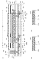
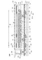
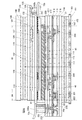
図1(A)及び図2に、表示装置の一例を示す。図1(A)は、表示装置100の断面図であり、図2は、表示装置100の斜視図である。図2では、明瞭化のため、偏光板130などの構成要素を省略して図示している。図2では、基板61を破線で示す。
本発明の一態様の表示装置が有する基板の材質などに大きな制限はなく、様々な基板を用いることができる。例えば、ガラス基板、石英基板、サファイア基板、半導体基板、セラミック基板、金属基板、またはプラスチック基板等を用いることができる。
本発明の一態様の表示装置が有するトランジスタは、トップゲート型またはボトムゲート型のいずれの構造としてもよい。または、チャネルの上下にゲート電極が設けられていてもよい。トランジスタに用いる半導体材料は特に限定されず、例えば、酸化物半導体、シリコン、ゲルマニウム等が挙げられる。トランジスタの半導体層には、可視光を透過する材料を用いることが好ましい。これにより、表示装置の開口率を高めることができる。
酸化物半導体層は、少なくともインジウム(In)、亜鉛(Zn)及びM(Al、Ti、Ga、Ge、Y、Zr、La、Ce、Nd、SnまたはHf等の金属)を含むIn−M−Zn酸化物で表記される膜を含むことが好ましい。また、該酸化物半導体を用いたトランジスタの電気特性のばらつきを減らすため、それらと共に、スタビライザーを含むことが好ましい。
表示装置が有する各絶縁層、オーバーコート、スペーサ等に用いることのできる絶縁材料としては、有機絶縁材料または無機絶縁材料を用いることができる。有機絶縁材料としては、例えば、アクリル樹脂、エポキシ樹脂、ポリイミド樹脂、ポリアミド樹脂、ポリアミドイミド樹脂、シロキサン樹脂、ベンゾシクロブテン系樹脂、及びフェノール樹脂等が挙げられる。無機絶縁層としては、酸化シリコン膜、酸化窒化シリコン膜、窒化酸化シリコン膜、窒化シリコン膜、酸化アルミニウム膜、酸化ハフニウム膜、酸化イットリウム膜、酸化ジルコニウム膜、酸化ガリウム膜、酸化タンタル膜、酸化マグネシウム膜、酸化ランタン膜、酸化セリウム膜、及び酸化ネオジム膜等が挙げられる。
トランジスタのゲート、ソース、ドレインのほか、表示装置が有する各種配線及び電極等の導電層には、アルミニウム、チタン、クロム、ニッケル、銅、イットリウム、ジルコニウム、モリブデン、銀、タンタル、またはタングステンなどの金属、またはこれを主成分とする合金を単層構造または積層構造として用いることができる。例えば、アルミニウム膜上にチタン膜を積層する二層構造、タングステン膜上にチタン膜を積層する二層構造、モリブデン膜上に銅膜を積層した二層構造、モリブデンとタングステンを含む合金膜上に銅膜を積層した二層構造、銅−マグネシウム−アルミニウム合金膜上に銅膜を積層する二層構造、チタン膜または窒化チタン膜と、そのチタン膜または窒化チタン膜上に重ねてアルミニウム膜または銅膜を積層し、さらにその上にチタン膜または窒化チタン膜を形成する三層構造、モリブデン膜または窒化モリブデン膜と、そのモリブデン膜または窒化モリブデン膜上に重ねてアルミニウム膜または銅膜を積層し、さらにその上にモリブデン膜または窒化モリブデン膜を形成する三層構造等がある。例えば、ソース電極225a及びドレイン電極225bを三層構造とする場合、一層目及び三層目には、チタン、窒化チタン、モリブデン、タングステン、モリブデンとタングステンを含む合金、モリブデンとジルコニウムを含む合金、または窒化モリブデンでなる膜を形成し、二層目には、銅、アルミニウム、金または銀、或いは銅とマンガンの合金等の低抵抗材料でなる膜を形成することが好ましい。なお、ITO、酸化タングステンを含むインジウム酸化物、酸化タングステンを含むインジウム亜鉛酸化物、酸化チタンを含むインジウム酸化物、酸化チタンを含むインジウム錫酸化物、インジウム亜鉛酸化物、ITSO等の透光性を有する導電性材料を用いてもよい。
接着層141としては、熱硬化樹脂、光硬化樹脂、または2液混合型の硬化性樹脂などの硬化性樹脂を用いることができる。例えば、アクリル樹脂、ウレタン樹脂、エポキシ樹脂、またはシロキサン樹脂などを用いることができる。
接続体242としては、例えば、異方性導電フィルム(ACF:Anisotropic Conductive Film)、または異方性導電ペースト(ACP:Anisotropic Conductive Paste)などを用いることができる。
着色層131は特定の波長帯域の光を透過する有色層である。着色層131に用いることのできる材料としては、金属材料、樹脂材料、及び顔料または染料が含まれた樹脂材料などが挙げられる。
遮光層132は、例えば、隣接する異なる色の着色層131の間に設けられる。例えば、金属材料、または、顔料もしくは染料を含む樹脂材料を用いて形成されたブラックマトリクスを、遮光層132として用いることができる。なお、遮光層132は、駆動回路部64など、表示部62以外の領域にも設けると、導波光などによる光漏れを抑制できるため好ましい。
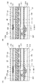
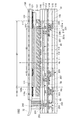
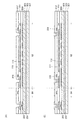
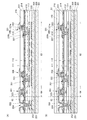
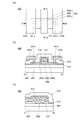
図5〜図8に、表示装置の一例をそれぞれ示す。図5は、表示装置100Aの断面図であり、図6は、本発明の一態様の表示装置が有する副画素の上面図であり、図7は、表示装置100Bの断面図であり、図8は、表示装置100Cの断面図である。なお、表示装置100A、表示装置100B、及び表示装置100Cの斜視図は、図2に示す表示装置100と同様であるため、ここでの説明は省略する。
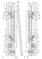
図8に示す表示装置100Cの作製方法の一例について、図9〜図13を用いて説明する。なお、トランジスタの作製方法の詳細は、実施の形態2を参照することができる。
図8に示す表示装置100Cの作製方法の一例について、図14及び図15を用いて説明する。
図8に示す表示装置100Cの作製方法の一例について、図16及び図17を用いて説明する。
図18(A)、図19(A)、及び図20に、表示装置の一例をそれぞれ示す。図18(A)は、表示装置100Dの断面図であり、図19(A)は、表示装置100Eの断面図であり、図20は、表示装置100Fの断面図である。なお、表示装置100D、表示装置100E、及び表示装置100Fの斜視図は、図2に示す表示装置100と同様であるため、ここでの説明は省略する。
本発明の一態様は、タッチセンサが搭載された表示装置(入出力装置またはタッチパネルともいう)に適用することができる。上述の各表示装置の構成を、タッチパネルに適用することができる。本実施の形態では、表示装置100Cにタッチセンサを搭載する例を主に説明する。
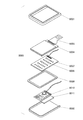
図24及び図25に、タッチパネルの一例を示す。図24(A)は、タッチパネル350Bの斜視図である。図24(B)は、図24(A)を展開した斜視概略図である。なお、明瞭化のため、代表的な構成要素のみを示している。図24(B)では、基板61を破線で輪郭のみ明示している。図25は、タッチパネル350Bの断面図である。
図26に、タッチパネルの一例を示す。図26は、タッチパネル350Cの断面図である。
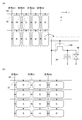
図30(A)、(B)に、液晶素子の電極の上面形状の例を示す。
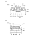
本実施の形態では、半導体装置について説明する。具体的には、本発明の一態様の表示装置に用いることのできるトランジスタ、及び当該トランジスタの作製方法について、図31乃至図40を用いて説明する。
図31(A)(B)(C)に、トランジスタの一例を示す。図31(A)(B)(C)に示すトランジスタは、スタガ型(トップゲート構造)である。
次に、図31(A)(B)(C)に示すトランジスタと異なる構成について、図32(A)(B)(C)を用いて説明する。
次に、図32(A)(B)(C)に示すトランジスタと異なる構成について、図33及び図34を用いて説明する。
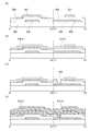
次に、図31に示すトランジスタ300の作製方法の一例について、図35乃至図37を用いて説明する。なお、図35乃至図37は、トランジスタ300の作製方法を説明するチャネル長(L)方向及びチャネル幅(W)方向の断面図である。
次に、図32に示すトランジスタ300Aの作製方法の一例について、図38乃至図40を用いて説明する。なお、図38乃至図40は、トランジスタ300Aの作製方法を説明するチャネル長(L)方向及びチャネル幅(W)方向の断面図である。
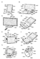
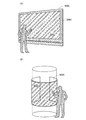
本実施の形態では、本発明の一態様の表示装置を有するタッチパネルモジュール及び電子機器について、図41〜図43を用いて説明する。
40 液晶素子
45 光
46 外光
51 基板
56 導電層
56a 導電層
56b 導電層
57 補助配線
58 導電層
60 画素
60a 副画素
60b 副画素
60c 副画素
61 基板
62 表示部
64 駆動回路部
65 配線
66 遮光領域
67 領域
68 開口部
69 接続部
72 FPC
72a FPC
72b FPC
73 IC
73a IC
73b IC
81 走査線
82 信号線
100 表示装置
100A 表示装置
100B 表示装置
100C 表示装置
100D 表示装置
100E 表示装置
100F 表示装置
111 画素電極
112 共通電極
113 液晶層
113a 配向膜
113b 配向膜
114 画素電極
115 導電層
117 スペーサ
118 導電層
119 補助配線
121 オーバーコート
123 絶縁層
124 電極
125 絶縁層
126 導電層
127 電極
128 電極
130 偏光板
131 着色層
132 遮光層
133 液晶層
133a 配向膜
133b 配向膜
138 配線
139 配線
141 接着層
142 接着層
160 保護基板
161 バックライト
162 基板
163 接着層
164 接着層
165 偏光板
166 偏光板
167 接着層
168 接着層
169 接着層
201 トランジスタ
204 接続部
206 トランジスタ
207 接続部
211 絶縁層
212 絶縁層
213 ゲート絶縁層
213_0 絶縁層
214 絶縁層
215 絶縁層
216 絶縁層
220 絶縁層
221 ゲート
221_0 導電層
222 導電層
222a 導電層
222b 導電層
223 ゲート
225a ソース電極
225b ドレイン電極
227 導電層
228 走査線
229 信号線
231 半導体層
231a チャネル領域
231b 低抵抗領域
242 接続体
242b 接続体
243 接続体
244 導電層
245 導電層
251 導電層
252 接続部
253 導電層
255 導電層
300 トランジスタ
300A トランジスタ
300B トランジスタ
300C トランジスタ
301 作製基板
302 基板
303 分離層
304 絶縁層
305 酸化物絶縁層
306 導電層
307 酸化物半導体層
308 酸化物半導体層
308d ドレイン領域
308f 領域
308i チャネル領域
308s ソース領域
309 分離層
310 絶縁層
310_0 絶縁層
312 導電層
312_0 導電層
316 絶縁層
318 絶縁層
320a 導電層
320b 導電層
340 マスク
341a 開口部
341b 開口部
343 開口部
350A タッチパネル
350B タッチパネル
350C タッチパネル
370 表示装置
375 入力装置
376 入力装置
379 表示装置
621 電極
622 電極
3501 配線
3502 配線
3510 配線
3510_1 配線
3510_2 配線
3510_6 配線
3511 配線
3511_1 配線
3511_6 配線
3515_1 ブロック
3515_2 ブロック
3516 ブロック
5000 筐体
5001 表示部
5002 表示部
5003 スピーカ
5004 LEDランプ
5005 操作キー
5006 接続端子
5007 センサ
5008 マイクロフォン
5009 スイッチ
5010 赤外線ポート
5011 記録媒体読込部
5012 スタンド
5013 リモコン操作機
5014 アンテナ
5015 シャッターボタン
5016 受像部
5017 充電器
5018 バンド
5019 留め金
5020 アイコン
5021 アイコン
8000 タッチパネルモジュール
8001 上部カバー
8002 下部カバー
8003 FPC
8004 タッチパネル
8007 バックライト
8008 光源
8009 フレーム
8010 プリント基板
8011 バッテリ
Claims (16)
- 液晶素子、トランジスタ、及び第1の絶縁層を有し、
前記液晶素子は、画素電極、共通電極、及び液晶層を有し、
前記トランジスタは、酸化物半導体層、ゲート、及びゲート絶縁層を有し、
前記第1の絶縁層は、前記画素電極と前記トランジスタの間に位置し、
前記第1の絶縁層は、開口部を有し、
前記画素電極は、前記液晶層と前記第1の絶縁層の間に位置し、
前記画素電極及び前記共通電極は、それぞれ、可視光を透過する機能を有し、
前記酸化物半導体層は、第1の領域と第2の領域を有し、
前記第1の領域は、前記ゲート絶縁層を介して前記ゲートと重なり、
前記第2の領域は、前記画素電極と接する第1の部分と、前記第1の絶縁層における開口部の側面と接する第2の部分と、を有し、
前記第2の領域の抵抗率は、前記第1の領域の抵抗率よりも低い、表示装置。 - 請求項1において、
前記画素電極の前記液晶層側の面は、前記第1の絶縁層の前記液晶層側の面と同一面を形成することができる、表示装置。 - 請求項1または2において、
前記共通電極は、前記トランジスタと前記液晶層との間に位置する、表示装置。 - 請求項3において、
第2の絶縁層を有し、
前記第2の絶縁層は、前記画素電極と前記共通電極の間に位置し、
前記共通電極の前記液晶側の面は、前記第2の絶縁層の前記液晶側の面と同一面を形成することができる、表示装置。 - 請求項1乃至4のいずれか一において、
画素を有し、
前記第1の部分は、前記画素の開口部と重なる、表示装置。 - 請求項1乃至5のいずれか一において、
前記画素電極及び前記酸化物半導体層は、インジウムと、亜鉛と、アルミニウム、ガリウム、イットリウム、及びスズのうち少なくとも一つと、を有する、表示装置。 - 請求項1乃至6のいずれか一において、
前記共通電極は、インジウムと、亜鉛と、アルミニウム、ガリウム、イットリウム、及びスズのうち少なくとも一つと、を有する、表示装置。 - 請求項1乃至7のいずれか一において、
前記画素電極及び前記酸化物半導体層は、結晶部を有する、表示装置。 - 請求項8において、
前記画素電極及び前記酸化物半導体層が有する結晶部は、c軸配向性を有する、表示装置。 - 請求項1乃至9のいずれか一において、
前記共通電極は、結晶部を有する、表示装置。 - 請求項10において、
前記共通電極が有する結晶部は、c軸配向性を有する、表示装置。 - 請求項1乃至11のいずれか一において、
前記トランジスタは、バックゲートを有し、
前記バックゲートは、前記酸化物半導体層を介して、前記ゲートと重なる部分を有し、
前記ゲート及び前記バックゲートは電気的に接続され、
前記ゲートは、インジウムと、亜鉛と、アルミニウム、ガリウム、イットリウム、及びスズのうち少なくとも一つと、を有する、表示装置。 - 請求項1乃至12のいずれか一において、
走査線及び信号線を有し、
前記走査線が伸長する方向は、前記信号線が伸長する方向と交差し、
同一の色を呈する複数の画素が配設される方向は、前記信号線が伸長する方向と交差する、表示装置。 - 第1の基板上に、分離層を形成する工程と、
前記分離層上に、島状の酸化物導電層を形成する工程と、
前記分離層上及び前記酸化物導電層上に、酸化物絶縁層を形成する工程と、
前記酸化物絶縁層上に、トランジスタを形成する工程と、
前記第1の基板と第2の基板を、接着層を用いて貼り合わせる工程と、
前記第1の基板と前記第2の基板を分離することで、前記酸化物導電層及び前記酸化物絶縁層を露出する工程とを有し、
前記酸化物導電層は、表示素子の電極として機能することができる、分離方法。 - 請求項14において、
前記酸化物導電層は、前記トランジスタと電気的に接続される、分離方法。 - 請求項14または15において、
前記トランジスタのチャネル領域は、インジウムと、亜鉛と、アルミニウム、ガリウム、イットリウム、及びスズのうち少なくとも一つと、を有する膜を用いて形成され、
前記酸化物導電層は、インジウムと、亜鉛と、アルミニウム、ガリウム、イットリウム、及びスズのうち少なくとも一つと、を有する膜を用いて形成される、分離方法。
Applications Claiming Priority (2)
| Application Number | Priority Date | Filing Date | Title |
|---|---|---|---|
| JP2015242518 | 2015-12-11 | ||
| JP2015242518 | 2015-12-11 |
Publications (3)
| Publication Number | Publication Date |
|---|---|
| JP2017111438A true JP2017111438A (ja) | 2017-06-22 |
| JP2017111438A5 JP2017111438A5 (ja) | 2020-01-23 |
| JP6863725B2 JP6863725B2 (ja) | 2021-04-21 |
Family
ID=59012729
Family Applications (1)
| Application Number | Title | Priority Date | Filing Date |
|---|---|---|---|
| JP2016236993A Active JP6863725B2 (ja) | 2015-12-11 | 2016-12-06 | 表示装置 |
Country Status (4)
| Country | Link |
|---|---|
| US (1) | US20170168333A1 (ja) |
| JP (1) | JP6863725B2 (ja) |
| KR (1) | KR20180093000A (ja) |
| WO (1) | WO2017098376A1 (ja) |
Cited By (4)
| Publication number | Priority date | Publication date | Assignee | Title |
|---|---|---|---|---|
| WO2019135147A1 (ja) * | 2018-01-05 | 2019-07-11 | 株式会社半導体エネルギー研究所 | 表示装置、表示モジュール、及び電子機器 |
| WO2019220246A1 (ja) * | 2018-05-18 | 2019-11-21 | 株式会社半導体エネルギー研究所 | 表示装置、表示モジュール、電子機器、及び、表示装置の作製方法 |
| US10955950B2 (en) | 2016-11-09 | 2021-03-23 | Semiconductor Energy Laboratory Co., Ltd. | Display device, display module, electronic device, and method for manufacturing the display device |
| JP2024037725A (ja) * | 2018-03-30 | 2024-03-19 | 株式会社半導体エネルギー研究所 | 表示装置 |
Families Citing this family (16)
| Publication number | Priority date | Publication date | Assignee | Title |
|---|---|---|---|---|
| KR102173801B1 (ko) | 2012-07-12 | 2020-11-04 | 가부시키가이샤 한도오따이 에네루기 켄큐쇼 | 표시 장치, 및 표시 장치의 제작 방법 |
| US10114263B2 (en) * | 2015-12-18 | 2018-10-30 | Semiconductor Energy Laboratory Co., Ltd. | Display device |
| KR102550696B1 (ko) * | 2016-04-08 | 2023-07-04 | 삼성디스플레이 주식회사 | 디스플레이 장치 |
| JP6655471B2 (ja) * | 2016-05-18 | 2020-02-26 | 株式会社ジャパンディスプレイ | 表示装置及びセンサ装置 |
| US10790318B2 (en) | 2016-11-22 | 2020-09-29 | Semiconductor Energy Laboratory Co., Ltd. | Display device, method for manufacturing the same, and electronic device |
| WO2018100466A1 (en) * | 2016-11-30 | 2018-06-07 | Semiconductor Energy Laboratory Co., Ltd. | Display device, display module, and electronic device |
| KR102566717B1 (ko) * | 2016-12-12 | 2023-08-14 | 삼성전자 주식회사 | 생체 센서를 구비한 전자 장치 |
| KR102772195B1 (ko) * | 2017-02-28 | 2025-02-26 | 삼성디스플레이 주식회사 | 표시 장치 및 표시 장치의 제조 방법 |
| CN110678989B (zh) | 2017-03-13 | 2024-02-13 | 株式会社半导体能源研究所 | 半导体装置及半导体装置的制造方法 |
| US10146080B1 (en) * | 2017-11-21 | 2018-12-04 | Wuhan China Star Optoelectronics Technology Co., Ltd. | Method for manufacturing display device |
| JP2019101056A (ja) * | 2017-11-28 | 2019-06-24 | 株式会社ジャパンディスプレイ | 表示装置およびヘッドアップ表示装置 |
| CN110120186A (zh) * | 2018-02-06 | 2019-08-13 | 南京瀚宇彩欣科技有限责任公司 | 显示模块 |
| JP7173154B2 (ja) * | 2018-09-19 | 2022-11-16 | 凸版印刷株式会社 | 調光シート、および、調光シートの製造方法 |
| TWI694280B (zh) * | 2019-03-05 | 2020-05-21 | 友達光電股份有限公司 | 顯示裝置及其製造方法 |
| US11488983B2 (en) * | 2019-07-22 | 2022-11-01 | Beijing Boe Technology Development Co., Ltd. | Array substrate, method for manufacturing the same, and display device |
| KR20240111850A (ko) * | 2023-01-10 | 2024-07-18 | 삼성디스플레이 주식회사 | 표시 장치 |
Citations (5)
| Publication number | Priority date | Publication date | Assignee | Title |
|---|---|---|---|---|
| JPH07169973A (ja) * | 1993-10-06 | 1995-07-04 | Matsushita Electric Ind Co Ltd | 薄膜トランジスタアレイとその製造方法およびこれを用いた液晶表示装置 |
| KR20080001896A (ko) * | 2006-06-30 | 2008-01-04 | 엘지.필립스 엘시디 주식회사 | 횡전계방식 액정표시장치 및 그 제조 방법 |
| JP2012208184A (ja) * | 2011-03-29 | 2012-10-25 | Japan Display Central Co Ltd | 液晶表示素子およびその製造方法 |
| WO2013191033A1 (ja) * | 2012-06-19 | 2013-12-27 | シャープ株式会社 | 半導体装置およびその製造方法 |
| US20160026044A1 (en) * | 2014-07-25 | 2016-01-28 | Lg Display Co., Ltd. | Display device and method of manufacturing the same |
Family Cites Families (15)
| Publication number | Priority date | Publication date | Assignee | Title |
|---|---|---|---|---|
| US6127199A (en) * | 1996-11-12 | 2000-10-03 | Seiko Epson Corporation | Manufacturing method of active matrix substrate, active matrix substrate and liquid crystal display device |
| JP5078246B2 (ja) | 2005-09-29 | 2012-11-21 | 株式会社半導体エネルギー研究所 | 半導体装置、及び半導体装置の作製方法 |
| JP5064747B2 (ja) | 2005-09-29 | 2012-10-31 | 株式会社半導体エネルギー研究所 | 半導体装置、電気泳動表示装置、表示モジュール、電子機器、及び半導体装置の作製方法 |
| JP2007250993A (ja) * | 2006-03-17 | 2007-09-27 | Kaneka Corp | 粉体の導電性高分子を電極に用いた電気化学素子 |
| EP2924498A1 (en) * | 2006-04-06 | 2015-09-30 | Semiconductor Energy Laboratory Co, Ltd. | Liquid crystal desplay device, semiconductor device, and electronic appliance |
| JP2009099887A (ja) * | 2007-10-19 | 2009-05-07 | Hitachi Displays Ltd | 表示装置 |
| JP5246782B2 (ja) * | 2008-03-06 | 2013-07-24 | 株式会社ジャパンディスプレイウェスト | 液晶装置および電子機器 |
| JP2010033038A (ja) * | 2008-06-30 | 2010-02-12 | Nec Electronics Corp | 表示パネル駆動方法及び表示装置 |
| KR101422362B1 (ko) * | 2009-07-10 | 2014-07-22 | 가부시키가이샤 한도오따이 에네루기 켄큐쇼 | 표시 장치, 표시 패널 및 전자 기기 |
| US20120231241A1 (en) * | 2009-11-18 | 2012-09-13 | Sharp Kabushiki Kaisha | Transparent electrode substrate, precursor transparent electrode substrate, and method for manufacturing transparent electrode substrate |
| US9443984B2 (en) * | 2010-12-28 | 2016-09-13 | Semiconductor Energy Laboratory Co., Ltd. | Semiconductor device and manufacturing method thereof |
| TWI562361B (en) * | 2012-02-02 | 2016-12-11 | Semiconductor Energy Lab Co Ltd | Semiconductor device |
| JP5906132B2 (ja) * | 2012-05-09 | 2016-04-20 | 株式会社ジャパンディスプレイ | 表示装置 |
| TWI690085B (zh) * | 2013-05-16 | 2020-04-01 | 日商半導體能源研究所股份有限公司 | 半導體裝置 |
| JP6417125B2 (ja) * | 2014-06-25 | 2018-10-31 | 株式会社ジャパンディスプレイ | 半導体装置 |
-
2016
- 2016-12-01 KR KR1020187017983A patent/KR20180093000A/ko not_active Ceased
- 2016-12-01 US US15/366,073 patent/US20170168333A1/en not_active Abandoned
- 2016-12-01 WO PCT/IB2016/057235 patent/WO2017098376A1/en not_active Ceased
- 2016-12-06 JP JP2016236993A patent/JP6863725B2/ja active Active
Patent Citations (6)
| Publication number | Priority date | Publication date | Assignee | Title |
|---|---|---|---|---|
| JPH07169973A (ja) * | 1993-10-06 | 1995-07-04 | Matsushita Electric Ind Co Ltd | 薄膜トランジスタアレイとその製造方法およびこれを用いた液晶表示装置 |
| KR20080001896A (ko) * | 2006-06-30 | 2008-01-04 | 엘지.필립스 엘시디 주식회사 | 횡전계방식 액정표시장치 및 그 제조 방법 |
| JP2012208184A (ja) * | 2011-03-29 | 2012-10-25 | Japan Display Central Co Ltd | 液晶表示素子およびその製造方法 |
| WO2013191033A1 (ja) * | 2012-06-19 | 2013-12-27 | シャープ株式会社 | 半導体装置およびその製造方法 |
| CN104396019A (zh) * | 2012-06-19 | 2015-03-04 | 夏普株式会社 | 半导体装置及其制造方法 |
| US20160026044A1 (en) * | 2014-07-25 | 2016-01-28 | Lg Display Co., Ltd. | Display device and method of manufacturing the same |
Cited By (19)
| Publication number | Priority date | Publication date | Assignee | Title |
|---|---|---|---|---|
| US10955950B2 (en) | 2016-11-09 | 2021-03-23 | Semiconductor Energy Laboratory Co., Ltd. | Display device, display module, electronic device, and method for manufacturing the display device |
| US11733574B2 (en) | 2018-01-05 | 2023-08-22 | Semiconductor Energy Laboratory Co., Ltd. | Display device, display module, and electronic device |
| US11940703B2 (en) | 2018-01-05 | 2024-03-26 | Semiconductor Energy Laboratory Co., Ltd. | Display device, display module, and electronic device |
| CN111542780A (zh) * | 2018-01-05 | 2020-08-14 | 株式会社半导体能源研究所 | 显示装置、显示模块及电子设备 |
| WO2019135147A1 (ja) * | 2018-01-05 | 2019-07-11 | 株式会社半導体エネルギー研究所 | 表示装置、表示モジュール、及び電子機器 |
| CN111542780B (zh) * | 2018-01-05 | 2023-11-21 | 株式会社半导体能源研究所 | 显示装置、显示模块及电子设备 |
| JP2024037725A (ja) * | 2018-03-30 | 2024-03-19 | 株式会社半導体エネルギー研究所 | 表示装置 |
| JP2025087777A (ja) * | 2018-03-30 | 2025-06-10 | 株式会社半導体エネルギー研究所 | 表示装置 |
| US12461418B2 (en) | 2018-03-30 | 2025-11-04 | Semiconductor Energy Laboratory Co., Ltd. | Display device |
| JP7289294B2 (ja) | 2018-05-18 | 2023-06-09 | 株式会社半導体エネルギー研究所 | 表示装置、表示モジュール、電子機器、及び、表示装置の作製方法 |
| JPWO2019220246A1 (ja) * | 2018-05-18 | 2021-07-15 | 株式会社半導体エネルギー研究所 | 表示装置、表示モジュール、電子機器、及び、表示装置の作製方法 |
| JP2023123443A (ja) * | 2018-05-18 | 2023-09-05 | 株式会社半導体エネルギー研究所 | 表示装置、表示モジュールおよび電子機器 |
| KR20210010520A (ko) * | 2018-05-18 | 2021-01-27 | 가부시키가이샤 한도오따이 에네루기 켄큐쇼 | 표시 장치, 표시 모듈, 전자 기기, 및 표시 장치의 제작 방법 |
| JP7441362B2 (ja) | 2018-05-18 | 2024-02-29 | 株式会社半導体エネルギー研究所 | 表示装置、表示モジュールおよび電子機器 |
| CN112136170A (zh) * | 2018-05-18 | 2020-12-25 | 株式会社半导体能源研究所 | 显示装置、显示模块、电子设备及显示装置的制造方法 |
| WO2019220246A1 (ja) * | 2018-05-18 | 2019-11-21 | 株式会社半導体エネルギー研究所 | 表示装置、表示モジュール、電子機器、及び、表示装置の作製方法 |
| US11961871B2 (en) | 2018-05-18 | 2024-04-16 | Semiconductor Energy Laboratory Co., Ltd. | Display device, display module, electronic device, and method for fabricating display device |
| JP2025026547A (ja) * | 2018-05-18 | 2025-02-21 | 株式会社半導体エネルギー研究所 | 表示装置 |
| KR102800959B1 (ko) * | 2018-05-18 | 2025-04-29 | 가부시키가이샤 한도오따이 에네루기 켄큐쇼 | 표시 장치, 표시 모듈, 전자 기기, 및 표시 장치의 제작 방법 |
Also Published As
| Publication number | Publication date |
|---|---|
| JP6863725B2 (ja) | 2021-04-21 |
| WO2017098376A1 (en) | 2017-06-15 |
| KR20180093000A (ko) | 2018-08-20 |
| US20170168333A1 (en) | 2017-06-15 |
Similar Documents
| Publication | Publication Date | Title |
|---|---|---|
| JP6863725B2 (ja) | 表示装置 | |
| JP6802701B2 (ja) | 表示装置、モジュール及び電子機器 | |
| JP7150906B2 (ja) | 半導体装置 | |
| JP7570478B2 (ja) | 半導体装置 | |
| CN109906405B (zh) | 显示装置、显示模块、电子设备以及显示装置的制造方法 | |
| JP6929079B2 (ja) | 半導体装置の作製方法 | |
| CN108121123B (zh) | 显示装置、显示模块及电子设备 | |
| JP7297984B2 (ja) | 表示装置、表示モジュールおよび電子機器 | |
| JP2019024105A (ja) | 半導体装置の作製方法 | |
| JP2024075612A (ja) | 表示装置 | |
| JP2018006734A (ja) | 半導体装置、当該半導体装置の作製方法、及び当該半導体装置を有する表示装置 | |
| KR20170129215A (ko) | 터치 패널 | |
| JP2017076788A (ja) | 半導体装置の作製方法 | |
| JP2017076787A (ja) | 半導体装置の作製方法 | |
| JP2012003238A (ja) | 液晶表示装置及びその駆動方法 | |
| JP2017228752A (ja) | 半導体装置の作製方法 | |
| JP2020080416A (ja) | 半導体装置 | |
| JP2022058513A (ja) | 表示装置 |
Legal Events
| Date | Code | Title | Description |
|---|---|---|---|
| A521 | Request for written amendment filed |
Free format text: JAPANESE INTERMEDIATE CODE: A523 Effective date: 20191204 |
|
| A621 | Written request for application examination |
Free format text: JAPANESE INTERMEDIATE CODE: A621 Effective date: 20191204 |
|
| A977 | Report on retrieval |
Free format text: JAPANESE INTERMEDIATE CODE: A971007 Effective date: 20200928 |
|
| A131 | Notification of reasons for refusal |
Free format text: JAPANESE INTERMEDIATE CODE: A131 Effective date: 20201006 |
|
| A521 | Request for written amendment filed |
Free format text: JAPANESE INTERMEDIATE CODE: A523 Effective date: 20201111 |
|
| TRDD | Decision of grant or rejection written | ||
| A01 | Written decision to grant a patent or to grant a registration (utility model) |
Free format text: JAPANESE INTERMEDIATE CODE: A01 Effective date: 20210309 |
|
| A61 | First payment of annual fees (during grant procedure) |
Free format text: JAPANESE INTERMEDIATE CODE: A61 Effective date: 20210401 |
|
| R150 | Certificate of patent or registration of utility model |
Ref document number: 6863725 Country of ref document: JP Free format text: JAPANESE INTERMEDIATE CODE: R150 |
|
| R250 | Receipt of annual fees |
Free format text: JAPANESE INTERMEDIATE CODE: R250 |
|
| R250 | Receipt of annual fees |
Free format text: JAPANESE INTERMEDIATE CODE: R250 |
|
| R250 | Receipt of annual fees |
Free format text: JAPANESE INTERMEDIATE CODE: R250 |