JP2017111990A - Switch built-in cable - Google Patents
Switch built-in cable Download PDFInfo
- Publication number
- JP2017111990A JP2017111990A JP2015245891A JP2015245891A JP2017111990A JP 2017111990 A JP2017111990 A JP 2017111990A JP 2015245891 A JP2015245891 A JP 2015245891A JP 2015245891 A JP2015245891 A JP 2015245891A JP 2017111990 A JP2017111990 A JP 2017111990A
- Authority
- JP
- Japan
- Prior art keywords
- conductor
- sheath
- conductor film
- shaped
- switch
- Prior art date
- Legal status (The legal status is an assumption and is not a legal conclusion. Google has not performed a legal analysis and makes no representation as to the accuracy of the status listed.)
- Granted
Links
Images








Classifications
-
- H—ELECTRICITY
- H01—ELECTRIC ELEMENTS
- H01H—ELECTRIC SWITCHES; RELAYS; SELECTORS; EMERGENCY PROTECTIVE DEVICES
- H01H13/00—Switches having rectilinearly-movable operating part or parts adapted for pushing or pulling in one direction only, e.g. push-button switch
- H01H13/70—Switches having rectilinearly-movable operating part or parts adapted for pushing or pulling in one direction only, e.g. push-button switch having a plurality of operating members associated with different sets of contacts, e.g. keyboard
- H01H13/702—Switches having rectilinearly-movable operating part or parts adapted for pushing or pulling in one direction only, e.g. push-button switch having a plurality of operating members associated with different sets of contacts, e.g. keyboard with contacts carried by or formed from layers in a multilayer structure, e.g. membrane switches
- H01H13/705—Switches having rectilinearly-movable operating part or parts adapted for pushing or pulling in one direction only, e.g. push-button switch having a plurality of operating members associated with different sets of contacts, e.g. keyboard with contacts carried by or formed from layers in a multilayer structure, e.g. membrane switches characterised by construction, mounting or arrangement of operating parts, e.g. push-buttons or keys
-
- H—ELECTRICITY
- H01—ELECTRIC ELEMENTS
- H01H—ELECTRIC SWITCHES; RELAYS; SELECTORS; EMERGENCY PROTECTIVE DEVICES
- H01H13/00—Switches having rectilinearly-movable operating part or parts adapted for pushing or pulling in one direction only, e.g. push-button switch
- H01H13/70—Switches having rectilinearly-movable operating part or parts adapted for pushing or pulling in one direction only, e.g. push-button switch having a plurality of operating members associated with different sets of contacts, e.g. keyboard
- H01H13/702—Switches having rectilinearly-movable operating part or parts adapted for pushing or pulling in one direction only, e.g. push-button switch having a plurality of operating members associated with different sets of contacts, e.g. keyboard with contacts carried by or formed from layers in a multilayer structure, e.g. membrane switches
- H01H13/703—Switches having rectilinearly-movable operating part or parts adapted for pushing or pulling in one direction only, e.g. push-button switch having a plurality of operating members associated with different sets of contacts, e.g. keyboard with contacts carried by or formed from layers in a multilayer structure, e.g. membrane switches characterised by spacers between contact carrying layers
-
- H—ELECTRICITY
- H01—ELECTRIC ELEMENTS
- H01H—ELECTRIC SWITCHES; RELAYS; SELECTORS; EMERGENCY PROTECTIVE DEVICES
- H01H13/00—Switches having rectilinearly-movable operating part or parts adapted for pushing or pulling in one direction only, e.g. push-button switch
- H01H13/70—Switches having rectilinearly-movable operating part or parts adapted for pushing or pulling in one direction only, e.g. push-button switch having a plurality of operating members associated with different sets of contacts, e.g. keyboard
- H01H13/702—Switches having rectilinearly-movable operating part or parts adapted for pushing or pulling in one direction only, e.g. push-button switch having a plurality of operating members associated with different sets of contacts, e.g. keyboard with contacts carried by or formed from layers in a multilayer structure, e.g. membrane switches
- H01H13/704—Switches having rectilinearly-movable operating part or parts adapted for pushing or pulling in one direction only, e.g. push-button switch having a plurality of operating members associated with different sets of contacts, e.g. keyboard with contacts carried by or formed from layers in a multilayer structure, e.g. membrane switches characterised by the layers, e.g. by their material or structure
-
- H—ELECTRICITY
- H01—ELECTRIC ELEMENTS
- H01H—ELECTRIC SWITCHES; RELAYS; SELECTORS; EMERGENCY PROTECTIVE DEVICES
- H01H3/00—Mechanisms for operating contacts
- H01H3/02—Operating parts, i.e. for operating driving mechanism by a mechanical force external to the switch
- H01H3/14—Operating parts, i.e. for operating driving mechanism by a mechanical force external to the switch adapted for operation by a part of the human body other than the hand, e.g. by foot
- H01H3/141—Cushion or mat switches
- H01H3/142—Cushion or mat switches of the elongated strip type
-
- H—ELECTRICITY
- H01—ELECTRIC ELEMENTS
- H01H—ELECTRIC SWITCHES; RELAYS; SELECTORS; EMERGENCY PROTECTIVE DEVICES
- H01H3/00—Mechanisms for operating contacts
- H01H3/02—Operating parts, i.e. for operating driving mechanism by a mechanical force external to the switch
- H01H3/14—Operating parts, i.e. for operating driving mechanism by a mechanical force external to the switch adapted for operation by a part of the human body other than the hand, e.g. by foot
- H01H3/141—Cushion or mat switches
- H01H3/142—Cushion or mat switches of the elongated strip type
- H01H2003/143—Cushion or mat switches of the elongated strip type provisions for avoiding the contact actuation when the elongated strip is bended
-
- H—ELECTRICITY
- H01—ELECTRIC ELEMENTS
- H01H—ELECTRIC SWITCHES; RELAYS; SELECTORS; EMERGENCY PROTECTIVE DEVICES
- H01H2211/00—Spacers
- H01H2211/006—Individual areas
Landscapes
- Push-Button Switches (AREA)
Abstract
【課題】曲げでは導通せず、指による加圧では導通するスイッチ内蔵ケーブルを提供する。【解決手段】第1の帯状基材を有し、その内面に第1の導体部が設けられた帯状の第1の導体膜と、この第1の導体膜と間隔を介し対向配置され、同じく内面に第2の導体部が設けられた帯状の第2の導体膜と、この第2の導体膜と前記第1の導体膜との間に設けられ、それらの間隔を保つ絶縁スペーサと、この絶縁スペーサが挟み込まれた前記第1、第2の導体膜にて構成され、スイッチ部材として機能する帯状導体膜を空洞部に内包する帯状のシースとを備え、前記帯状導体膜を構成する第1の導体膜は前記絶縁スペーサの上に移動可能に重ねられ、かつ前記シースの空洞部は、収められる前記帯状導体膜に対し、シースの曲げにより生ずる少なくとも前記第1の帯状基材の長さ方向の相対的ずれを許容する隙間を設けた構成とし、曲げに対し導通しないようにした。【選択図】図1A switch built-in cable that does not conduct when bent and conducts when pressed by a finger is provided. A strip-shaped first conductor film having a first strip-shaped base material, the first conductor portion being provided on the inner surface of the substrate, and the first conductor film disposed opposite to each other with a gap therebetween. A band-shaped second conductor film having a second conductor portion provided on the inner surface, an insulating spacer provided between the second conductor film and the first conductor film, and maintaining an interval therebetween; The first and second conductor films are configured by the first and second conductor films sandwiched with insulating spacers, and include a strip-shaped sheath that encloses a strip-shaped conductor film functioning as a switch member in a hollow portion, and constitutes the strip-shaped conductor film. The conductive film is movably overlaid on the insulating spacer, and the sheath cavity is at least in the length direction of the first belt-shaped substrate generated by bending the sheath with respect to the band-shaped conductive film to be accommodated. With a gap to allow relative displacement of It was not allowed to conduct against. [Selection] Figure 1
Description
本発明は、曲げでは導通せず、指による加圧では容易に導通し、例えばイヤホン付属スイッチとして用いると好適なスイッチ内蔵ケーブルに関する。 The present invention relates to a cable with a built-in switch that does not conduct when bent and easily conducts when pressed with a finger, and is suitable for use as an earphone-attached switch, for example.
CDプレーヤーやMDプレーヤーのような携帯型音楽プレーヤーや携帯情報端末などの機器はイヤホンやヘッドホンを用いて音を聞くことが一般的である。機器とイヤホンとの間は、一般的にケーブルで接続される。 Devices such as portable music players such as CD players and MD players and portable information terminals generally listen to sound using earphones or headphones. Generally, a cable is connected between the device and the earphone.
この場合、通常、ケーブルの途中に、音量調整やプレーヤーの動作制御(選曲やON・OFF等)を行うコントロールボックスが設けられ、コントロールボックスにスイッチが設けられている。また、無線機能を搭載したイヤホン本体では、イヤホン本体にスイッチが設けられている。 In this case, usually, a control box for adjusting the volume and controlling the player's operation (music selection, ON / OFF, etc.) is provided in the middle of the cable, and a switch is provided in the control box. In addition, in an earphone main body equipped with a wireless function, a switch is provided in the earphone main body.
リスナーが携帯型の機器でイヤホンを使う場合はジョギングやその他何らかの作業をしながら利用することが多い。これらの状況で再生機の制御等のスイッチ操作を行うに当たり、そのスイッチの位置がケーブルの一点に限定されているとその位置を探すなどして操作しなければならないため、迅速性に欠け、また、操作が煩わしく感じられることがある。 When a listener uses an earphone with a portable device, it is often used while jogging or doing some other work. Under these circumstances, when performing switch operations such as control of a regenerator, if the position of the switch is limited to one point of the cable, it must be operated by searching for that position, etc. The operation may feel troublesome.
したがって、ケーブル自体にケーブル機能をもたせ、外部から加圧することにより容易に導通状態となるようにすると、場所が特定されることがなく、スイッチ操作が容易になり、使い勝手が良好となる。 Therefore, when the cable itself is provided with a cable function and is easily brought into a conductive state by applying pressure from the outside, the location is not specified, the switch operation is facilitated, and the usability is improved.
このようなケーブルとしては、外皮内部に、2つの導電性部材が上下に互いに離間して対向配置され、その間に導電性ゴムが設けられ、外部からの加圧によって2つの導電性部材が接触して導通し、スイッチがONするようにしたものがある。(特許文献1) In such a cable, two conductive members are arranged in the outer casing so as to be spaced apart from each other, and a conductive rubber is provided between them, and the two conductive members are brought into contact with each other by external pressure. Some switches are turned on and the switch is turned on. (Patent Document 1)
また、外皮内部に、導電ゴムで被覆された2つの導電性部材が離間して配置され、外部からの加圧によって2つの導電性部材が接触し導通するようにしたものがある(特許文献2)。 In addition, there are two conductive members covered with conductive rubber that are spaced apart from each other inside the outer skin so that the two conductive members come into contact with each other by external pressure (Patent Document 2). ).
さらに、帯状の第1の基材と、この第1基材とを対向させ、内面の一方の側に平面状の+側電極を、他方の側に−側電極を設け、この+側電極と−側の電極間に相互を分離し絶縁する隙間が形成された第2の基材とを備え、前記+側電極および−側電極上に設けられたスペーサにより長さ方向に所定間隔で配される略矩形の窓を形成し、前記導体を介し前記+側電極と−側電極とを導通可能としたケーブルスイッチがある(特許文献3)。 Furthermore, the belt-shaped first base material and the first base material are opposed to each other, a flat + side electrode is provided on one side of the inner surface, and a − side electrode is provided on the other side. And a second base material formed with a gap for separating and insulating each other between the negative electrodes, and are arranged at predetermined intervals in the length direction by spacers provided on the positive electrode and the negative electrode. There is a cable switch in which a substantially rectangular window is formed and the + side electrode and the − side electrode can be conducted through the conductor (Patent Document 3).
特許文献1、2の先行技術では導電ゴムを備え、導電ゴムを用いたものは屈曲により抵抗値が下がり、意図しない動作をしてしまうおそれがある、という課題があった。また、手による加圧ではなく、曲げた場合、電極が接触し導通してしまうことがあり、誤動作を生じ易い、という課題があった。
In the prior arts of
特許文献3では曲げの伴う使用状態においても意図しない導通が発生することはない。しかしながら、一つの基材内面に+側電極と−側電極を向い合せて配置するが、この場合、各電極を波形または矩形にして向い合せ、その間に設ける絶縁用のスリットも同様な形状にしなければならず、構成が複雑であるという課題がある。
In
この発明は、上記のことに鑑み提案されたもので、その目的とするところは、電極構造を容易化し、かつ曲げによる変形ではより導通しにくく、あるいは導通することなく、指による加圧では容易に導通し得るようにしたケーブル内蔵スイッチを提供することにある。 The present invention has been proposed in view of the above, and the object of the invention is to facilitate the electrode structure and make it less conductive when deformed by bending, or easily by pressing with a finger without conducting. It is an object of the present invention to provide a switch with a built-in cable that can be connected to a cable.
請求項1に係る本発明は、第1の帯状基材を有し、その内面に第1の導体部が設けられた帯状の第1の導体膜と、この第1の導体膜と間隔を介し対向配置され、同じく内面に第2の導体部が設けられた帯状の第2の導体膜と、この第2の導体膜と前記の第1の導体膜との間に設けられ、それらの間隔を保つ絶縁スペーサと、この絶縁スペーサが挟み込まれた前記第1、第2の導体膜にて構成され、スイッチ部材として機能する帯状導体膜を空洞部に内包する帯状のシースとを備え、前記帯状導体膜を構成する第1の導体膜は前記絶縁スペーサの上に移動可能に重ねられ、かつ前記シースの空洞部は、収められる前記帯状導体膜に対し、シースの曲げにより生ずる少なくとも前記第1の帯状基材の長さ方向の相対的ずれを許容する隙間を設けたことを特徴とする。
請求項2に係る本発明は、請求項1記載のスイッチ内蔵ケーブルスイッチにおいて、前記シース空洞部の内壁と前記帯状導体膜との間隔を、前記帯状導体膜の幅中心付近を幅端部付近よりも大きく形成したことを特徴とする。
請求項3に係る本発明は、請求項1または2記載のスイッチ内蔵ケーブルにおいて、前記シースの幅両端部に形成した導線挿入孔に導線を設けたことを特徴とする。
請求項4に係る発明は、請求項1、2または3記載のスイッチ内蔵ケーブルにおいて、前記シースの両端部にそれぞれ膨設部を形成するとともに各膨設部間に溝を形成し、このシース外周に移動自在な横長リング状のスイッチ用加圧部材を設け、このスイッチ用加圧部材に外力により前記溝の底部を加圧する加圧用突部を設けたことを特徴とする。
The present invention according to
According to a second aspect of the present invention, in the cable switch with a built-in switch according to the first aspect, the distance between the inner wall of the sheath cavity and the strip-shaped conductor film is determined from the vicinity of the width center of the strip-shaped conductor film. It is also characterized by being formed large.
According to a third aspect of the present invention, in the cable with a built-in switch according to the first or second aspect, a conductive wire is provided in a conductive wire insertion hole formed at both ends of the width of the sheath.
According to a fourth aspect of the present invention, in the switch built-in cable according to the first, second, or third aspect, a bulging portion is formed at each end of the sheath and a groove is formed between the bulging portions, and the outer periphery of the sheath The switch pressure member having a horizontally long ring shape that is freely movable is provided, and the pressure protrusion for pressing the bottom of the groove by an external force is provided on the switch pressure member.
請求項1記載の本発明によれば、曲げた場合、それに応じて第1の導体膜が第2の導体膜側に変形することなく第2の導体膜上に設けられた絶縁スペーサに対し、長さ方向にずれ、また、両者間に間隔を保持する絶縁スペーサがあるため、第1、第2の導体部が接触し導通することはなく、誤動作を起こすことはない。
請求項2記載の本発明によれば、帯状導体膜とシース内壁との間にスペースがあり、加圧した際に第1、第2の導体部が接触するまでのストロークが大きくなるため、ユーザーが指で押した場合にその感触が判り易いスイッチを構築できる。
請求項3記載の本発明によれば、スイッチ内蔵の信号伝達ケーブルを容易に実現できる。
請求項4記載の本発明によれば、シースに膨設部を形成し、シースそのものを指で加圧しても導通しないようにし、シース外周に移動自在なスイッチ用加圧部材を設け、このスイッチ用加圧部材にシースを加圧する加圧用突部を設けたため、スイッチの位置を任意の位置に特定させ導通させることができる。
According to the first aspect of the present invention, when bent, the insulating film provided on the second conductor film without deforming the first conductor film to the second conductor film side accordingly, Since there is an insulating spacer that shifts in the length direction and maintains a gap between them, the first and second conductor portions do not come into contact with each other and do not cause malfunction.
According to the second aspect of the present invention, there is a space between the strip-shaped conductor film and the sheath inner wall, and the stroke until the first and second conductor portions come into contact with each other when pressurized is increased. It is possible to construct a switch that is easy to understand when the button is pressed with a finger.
According to the third aspect of the present invention, a signal transmission cable with a built-in switch can be easily realized.
According to the fourth aspect of the present invention, the bulging portion is formed in the sheath so that the sheath itself does not conduct even when it is pressurized with a finger, and a switch pressing member is provided on the outer periphery of the sheath. Since the pressurizing projection for pressurizing the sheath is provided on the pressurizing member, the position of the switch can be specified at an arbitrary position and can be conducted.
図1は本発明の第1実施例にかかる偏平タイプであって屈曲自在なスイッチ内蔵ケーブルの内部構造を示す概略縦断図を示す。 FIG. 1 is a schematic longitudinal cross-sectional view showing the internal structure of a flat cable of a flat type that can be bent according to a first embodiment of the present invention.
このスイッチ内蔵ケーブル1は、スイッチとして機能する帯状導体膜2と、この外周を覆う偏平であってチューブ状のシース3とを備えている。
The switch built-in
上記帯状導体膜2は、図示の状態において上側に位置する第1の導体膜4と、この第1の導体膜4と離間して対向配置された、下側に位置する第2の導体膜5と、これら第1、第2の導体膜4、5の間に設けられた絶縁スペーサ6とにて構成されている。
The strip-shaped
上記第1の導体膜4は、絶縁部材からなる第1の帯状基材4aと、この第1の帯状基材4aの内面(図示の状態において下面の相当)に帯状に設けられた第1の導体部4bによって構成されている。
The
上記第2の導体膜5は、同じく絶縁部材からなる第2の帯状基材5aと、この第2の帯状基材5aの内面(図示の状態において上面に相当)に帯状に設けられた第2の導体部5bによって構成されている。
The
これらの間に配置される絶縁スペーサ6は第1、第2の導体膜4、5の各帯状基材4a、5aが接触しないよう相互の間隔を保持する働きをなす。
The insulating
偏平であって帯状の屈曲自在なシース3はTPE(熱可塑性エラストマー)からなり、このシース3は第1、第2の導体膜4、5、および絶縁スペーサ6からなる帯状導体膜2を挿通可能な略矩形の空洞部3aを内部に有している。なお、空洞部3aの断面形状は矩形に限定されるものではない。なお、空洞部3aの両外側、すなわちシース3の幅両端部に導線挿通孔3bを形成しておくと好ましい。すなわち、そこに導線を挿通することにより容易にスイッチを内蔵した信号伝達ケーブルを得ることができるためである。
The flat and strip-like
空洞部3aは帯状導体膜2を余裕を持って内装できるよう帯状導体膜2の外形より大に形成されている。なお、空洞部3aの横幅は絶縁スペーサ6が第1、第2の帯状基材4a、5a間を維持できる程度に最小限にする必要がある。
The
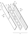
図2は帯状導体膜2の各構成部材の斜面図である。第1の導体膜4を構成する第1の帯状基材4aの内面には第1の導体部4bが設けられ、第1の導体部4bの端部にはリード部4c、接続電極4dが形成されている。第2の導体膜5を構成する第2の帯状基材5aの内面にも同様に第2の導体部5bが設けられ、その端部に同じくリード部5c、接続電極5dが形成されている。
FIG. 2 is a perspective view of each constituent member of the strip-shaped
絶縁スペーサ6は所定の厚みを有し、長さ方向に沿って所定の間隔で、例えば矩形形状の窓6aが形成され、梯子状に形成されている。
The insulating
上記において、一具体例として、第1、第2の帯状基材4a、5aはその材料としてPET(ポリエチレンテレフタレート)を用い、好ましくはフィルム厚み100μmとし、幅3mmとした。その他、PI(ポリイミド)等公知のFPC用の基板材料を用いても良い。
In the above, as a specific example, the first and second belt-
第1、第2の導体部4b、5bは、第1、第2の導体膜内面にそれぞれ銀ペーストを印刷し、かつスイッチ機能を持たせるために意図した部分の長さ方向全体および幅方向全体に導体部を設ける。さらに、第1、第2の帯状基材4a、5aの内面の端部には接続電極4d、5dを印刷し、かつこの接続電極4d、5dと前記印刷した第1、第2の導体部4b、5bとの間にはリード部4c、5cを形成し、電気的に接続している。
The first and
絶縁スペーサ6としては、ポリエステルフィルム50μmを用いた。他に、PIや紙等の絶縁物が使用できる。なお、当例の絶縁スペーサ6に代えて、一般的なFPCに用いられるソルダーレジストやカバーレイを採用することも可能である。その例については後述の実施例3で示す。
A polyester film of 50 μm was used as the insulating
また、導体部5bの長さ方向の3.5mm間隔で両側にそれぞれ形成した絶縁部6bをつなぐ1mm幅の桟状の絶縁部6cを設け、結果として、3.5mm間隔で略矩形型の窓6aを形成した。これは絶縁部6bを各第1、第2の導体部4b、5b間の幅方向の両側に安定して維持でき、かつ、指で押圧した場合に各導体膜4、5の導体部が接触可能な窓を設けるためのものであり、同様の効果があれば窓の形状は限定されない。
In addition, there are provided 1-mm-wide cross-shaped insulating
なお、絶縁スペーサ6及び各第1、第2の導体膜4、5はそれぞれ同幅とし、シース3内に収められた状態において絶縁スペーサ6が各第1、第2の膜4、5間の幅方向の両側に安定して位置するようにした。
The insulating
シース3内の空洞部3aは断面幅3.5mm×高さ0.8mmとし、内蔵する絶縁スペーサ6とを重ね断面寸法に対して幅、高さともに余裕のある寸法とする。なお、各部材寸法はスイッチ内蔵ケーブル1の大きさにより適宜最適な寸法とすることは言うまでもない。
The
帯状導体膜2の組立てにあたっては、図3(a)に示すように、第2の帯状基材5aの第2の導体部5b上に絶縁スペーサ6を重ね置き、図3(b)に示すように、その上に第1の帯状基材4aを重ねれば良い。すなわち、第1の帯状基材4aは少なくとも第1、第2の導体膜4、5上の導体部が互いに接触可能な部分においては単に重ねるだけで絶縁スペーサ6に対し長さ方向に可動自在とし、絶縁スペーサ6に対し固定し、一体化されるものではない。
In assembling the strip-shaped
図4(a)は組み立てられた帯状導体膜2の概略側断面を示す。この図4(a)や上記図1において、絶縁スペーサ6を第2の導体部5b上に接合することなく重ね、かつその上に第1の帯状基材4を重ねる状態を示す。各部材は接合、固定されないことを示すために図において各部材間に隙間を示している。しかしながら、実際は、図4(b)のような状態で重ね合わせられる。
FIG. 4A shows a schematic side cross-section of the assembled strip-shaped
組み立てられた帯状導体膜2は、図5に示すように、シース3の空洞部3aに収められる。図6は帯状導体膜2がシース3の空洞部3aに内包された概略斜視図を示す。帯状導体膜2が内包されたシース3は屈曲自在となっている。この場合、第1、第2導体膜4、5に曲げが生じた場合に、それぞれが円柱側面形状になるようにするためには、少なくともスイッチ動作部(各第1、第2の導体部4b、5bが対向している部分)で各導体膜間の長さ方向のずれを許容する必要がある。ただ、全く固定しない状態でシース3内に収めると、第1、第2の導体膜4、5の長さ方向の位置関係が、対面しないような位置まで大きくずれることになる可能性もあるため、また、シース3に挿入する場合の作業性の問題もあるため、実施例では長さ方向の端部で各導体膜間を、例えば感圧接着剤または両面テープ(図示せず)で固定する。なお、シース3の空洞部3aの長さの設定によりシース3に内装した状態で各導体膜4、5の導体部4b、5bが所定の範囲に維持できる場合は各導体膜間の固定は必須ではない。
The assembled strip-shaped
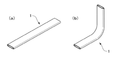
図7(a)は完成された帯状のスイッチ内蔵ケーブル1の概略斜視図を示す。このスイッチ内蔵ケーブル1は図7(b)に示すように、任意の部分で屈曲自在となっている。
FIG. 7A shows a schematic perspective view of the completed belt-like switch built-in
図8はスイッチ内蔵ケーブル1を曲げた場合における帯状導体膜2の状態を示す。本発明では曲げ状態において第1の導体部4bと第2の導体部5bとが接触しスイッチが動作しないようにしたことに特徴を有している。
FIG. 8 shows a state of the strip-shaped
すなわち、シース3に内包され、ケーブルスイッチとして機能する帯状導体膜2は、導体部4b、5bを内面に備えた第1、第2の帯状基材4a、5aの少なくとも2枚を使用し、それぞれの第1、第2の導体部4b、5bが接触しない程度に間隔を保って対向するように絶縁スペーサ6を挟み重ね合わせられる。その際、一定間隔を保つための絶縁スペーサ6は帯状導体膜2の第1、第2の導体部4b、5bが対向する部分の幅方向の両側に設けられ、かつ少なくともケーブルスイッチとして機能する部分すなわち第1の導体膜4の第1の導体部4bと第2の導体膜5の第2の導体部5bが対向している部分では、導体膜4、5と絶縁スペーサ6間は固定せず第1の導体膜4と第2の導体膜5の長さ方向の相対的な位置ずれを許容できるようにしている。このように構成すれば、帯状導体膜2の第1、第2の導体部4b、5bが対向する部分は、ケーブルに曲げが発生しても、この部分での各第1、第2の導体膜4、5の形状はそれぞれ形状剛性の大きい円柱側面形状となり、各円柱側面の上下に相当する部分に存在する絶縁スペーサbによりそれぞれの導体部の間隔は絶縁スペーサ6の厚み分保持され、導体部は接触して導通することはなく、曲げによる誤作動を防ぐことができる。
That is, the strip-shaped
これに加え、シース3に帯状導体膜2が内包された状態において、曲げが生じた場合に互いの第1、第2の導体部4b、5bが接触しないようにするため、各導体部4b、5bが対向する部分付近において長さ方向のずれを許容できるように帯状導体膜2はシース3内に余裕をもって収められている。
In addition to this, in the state where the strip-shaped
この状態において、スイッチ内蔵ケーブルが外力により曲げられた場合、上述のように、屈曲部では第1の導体膜4、第2の導体膜5共に円柱側面形状となるが、円柱側面の上下に位置する部分に存在する絶縁スペーサ6によって各導体膜4、5の間隔は維持される。また、屈曲部では曲げの内側の導体膜4の曲げRの長さが曲げ外側の導体膜5の曲げRの長さより短いため、その長さの差の分だけ第1、第2の導体膜4、5の間に長さの方向のずれが生じる。すなわち、曲げの内側となる第1の導体膜4は曲げ外側の第2導体膜5よりも曲げ部から離れる方向にずれが生じる。したがって、第1の導体部4bと第2の導体部5bは接触し導通することはない。
In this state, when the switch built-in cable is bent by an external force, as described above, both the
なお、図9に示すように、破線の長円形Aで囲んで示すように、各第1、第2の導体膜4、5が長さ方向にずれないように絶縁スペーサ6に固定してしまうと、長さ方向のずれが許容されなくなり、屈曲時に第1、第2の導体膜4、5の曲げ内側と曲げ外側周長の差により曲げの部分で各導体部が接触する方向に変形する力が発生し、曲げによってスイッチ機能が意図せず働いてしまう。
In addition, as shown in FIG. 9, the first and
また、図10に示すように、帯状導体膜2の両側部と、これと対向する空洞部3aの内壁との間に、破線の長円形Bで囲んで示すように、第1、第2の導体膜4、5の側端部がシース内壁と固定されてしまったような状態では、やはり屈曲時に対向する第1、第2の導体部4b、5bが接触する方向に変形が生じやすく、導通して誤作動を起こすおそれがある。
Further, as shown in FIG. 10, between the both side portions of the strip-shaped
したがって、本発明では前述のように、シース3の空洞部3aの内寸は少なくとも想定される曲げにおいて発生するずれの発生が許容されるよう、シース3の空洞部3aの厚み方向寸法を、シース3内に内包する帯状体膜2の厚みに対し大きく設定している。すなわち、本実施例のように各導体膜4、5間はその端部で固定されている場合、この状態でシース3内でのずれを許容するためには、ずれが発生した場合に曲げ部以外で生じる波状部をストレスなく許容できる程度の隙間をケーブル厚み方向に設けている。
Therefore, in the present invention, as described above, the dimension in the thickness direction of the
すなわち、図11に示すように、各導体膜4、5の端部が固定されていない場合、屈曲時に、破線の丸で囲んだ部分Cにおいて矢印間の寸法L1で示すように、導体膜4、5間にズレが生じるため、導体膜が波状になることはない。
That is, as shown in FIG. 11, when the end portions of the
しかしながら、図12に示すように、各導体膜4、5の端部を固定した場合、曲げると、破線の長円部分に示すように、内側の導体膜4が撓み、L2で示すように波状部が生じる。このため、シース3の空洞部3aに、波状部の厚み分L2を許容できる隙間をケーブル厚み方向にもたせている。
However, as shown in FIG. 12, when the end portions of the
なお、ケーブルに曲げが生じた場合に、内部の第1、第2の導体膜4、5が剛性の高い円柱形状で各導体部4b、5b間が非接触状態で保持できたとしても、シース3自体は必ずスイッチ動作の方向に変形する。これは、シース3の変形度合いが大きい場合やシース3の厚みが厚く変形圧力が高い場合は、第1、第2の導体膜4、5の円柱側面形状の剛性を上回って、各導体部4b、5b間が保持できなくなる可能性をもっているということになる。したがって、誤動作を防ぐためには、実際の(または想定される)変形がおきても、円柱部剛性がシース変形圧力に負けない程度に設定する必要がある。その方法としてはシース3を柔らかく、薄く、また、導体基材を厚く硬くすれば良いが、その程度は各要素の兼ね合いとなる。そのためこの部分は、実験により、およびもしくは有限要素法などを用いたシミュレーションにより求めれば良い。
Even if the first and
図13は、帯状導体膜2の上下面と、これと対向するシース3の空洞部3aの内壁との間の間隔をシース3の幅中心付近を幅端部付近より大きくした例を示す。
FIG. 13 shows an example in which the distance between the upper and lower surfaces of the strip-shaped
一具体例として、シース3の空洞部3aの高さを第1、第2の導体膜4、5の端部では0.8mm、中央部は1.3mmとした。これによると、加圧時に第1の導体膜4の第1の導体部4bと、第2の導体膜5の第2の導体部5bとが接触するまでのストロークが大きくなるため、ユーザーが指で押した場合にその感触が判り易いスイッチを構築できる。
As a specific example, the height of the
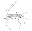
図14はスイッチ内蔵ケーブル1の上面、下面を、例えば人差し指F1,親指F2で挟み、加圧してシース3をつぶした場合を示す。第1の導体部4bを例えば+側電極、第2の導体部5bを−側電極とした場合、絶縁スペーサ6の窓内の中央部分において相互の導体部4b、5bが指による加圧により接触し、導通する。
FIG. 14 shows a case where the upper surface and the lower surface of the switch built-in
図15は絶縁スペーサ6の窓形状の変形例を示す。(a)図は窓形状を一般的な矩形とした例である。(b)図は、窓形状をより長方形とした例、(c)図は直線部と桟状の連結部を分割し、セグメント状とした例である。窓形状は、その他、トラック形状、長円形等としても良い。なお、窓形状により、指による押圧に対するスイッチとしての感度を調整することが可能である。すなわち、窓部が大きければ高感度(低圧で動作)、小さければ低感度(高圧で動作)、また、長さ方向に窓数を増やせば(窓間の絶縁部の数を増やす)低感度、減らせば高感度にできる。
FIG. 15 shows a modification of the window shape of the insulating
図16は本発明の第2実施例を示す。この実施例では、例えば図示の状態において、帯状導体膜2Aの下側の第2の導体部5bの中央にスリット5eを形成し、2分割構造とし、分割された導体部5bの一方を+電極、他方を−電極とし、かつ対向する第1の導体部4bをジャンパ部としたことに特徴を有している。
FIG. 16 shows a second embodiment of the present invention. In this embodiment, for example, in the state shown in the figure, a
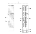
図17は上記第2実施例の帯状導体膜2Aの各部材を展開して示した図を示す。第2の導体部5bを直線状の+電極、−電極との2分割構造としたため、両側の各導体部5bの端部にそれぞれリード部5c、接続電極5dを設けている。したがって、第1の導体膜4の第1の導体部4bにはリード部、接続電極は必要ない。第1実施例では、図2に示したように、第1、第2の導体部4b、5bそれぞれに接続電極4d、5dを設けていたのに対し、この実施例では一方の導体膜にのみ一対の接続電極を設けたため、接続部分が一カ所となり、コネクタの数の削減や小型化が可能となる利点がある。
FIG. 17 shows a developed view of each member of the strip-shaped
絶縁スペーサ6の構造は第1実施例と同様である。絶縁スペーサ6を第2導体膜5に重ねると、窓6aの中央部にスリット5eが位置し、その両側に第2の導体部5bがそれぞれ露出し、押圧により第1の導体部4bが第2の各導体部5bに接触可能となっている。
The structure of the insulating
なお、第1の導体部4b側を+極、−極の2分割構造としても良いことは勿論である。
Needless to say, the
他の構成、作用は前述の第1実施例と同様である。 Other configurations and operations are the same as those of the first embodiment.
図18は本発明の第3実施例を示す。この実施例では、上記第2実施例において、2分割の第2導体部5bの上にレジストにより絶縁スペーサ6Aを形成したことに特徴を有している。この場合、一般的なFPCに用いられるソルダーレジストやカバーレイなどを施す方法を採用することが望ましい。すなわち、レジストやカバーレイは、基材や導体部に接着剤を介して直接接合固定されるため、曲げが想定されているFPC用のものは導体膜の変形時に導体部や基材に過度な応力が掛からないように、かつ、使用状態において、絶縁部が部分的に剥がれおちることの無いよう、柔軟な材料で基材よりも充分薄く形成される。更に、レジストタイプの場合は、スペーサタイプのように一体である必要はなく、図15(C)に示すように分割部を設けても良い。このようにすれば曲げが発生した場合にレジストが固定されている導体膜に発生する応力は減少し、円柱側面形状が形成しやすくなり誤動作を防ぐ効果がある。ただし、必要以上に隙間を大きくすることにより、曲げ時に各導体膜が接触しやすくならないように注意が必要である。
FIG. 18 shows a third embodiment of the present invention. This embodiment is characterized in that, in the second embodiment, the insulating
図19は帯状導体膜2を展開した状態を示す。
FIG. 19 shows a state in which the strip-shaped
その他の構成は第2実施例と同様である。このようなスイッチ内蔵ケーブル1を曲げても、第1、第2実施例と同様、絶縁スペーサ6A上に重ねられた第1の導体部4bは第2の導体部5b、5bに接触することはない。なお、図20は第3実施例において曲げが発生した状態を示す。
Other configurations are the same as those of the second embodiment. Even if such a switch built-in
図21は第3実施例のスイッチ内蔵ケーブル1を指により加圧し、第1の導体部4bの中央部を各第2の導体部5b、5bに接触させ導通させた状態を示す。
FIG. 21 shows a state in which the switch built-in
図22は本発明の第4実施例を示す。前述の第1〜3実施例ではスイッチ内蔵ケーブルの長さ方向のどの部分を指で加圧しても導通させることが出来たが、この実施例では所定の位置でのみ導通させるようにしたことに特徴を有している。 FIG. 22 shows a fourth embodiment of the present invention. In the first to third embodiments described above, any portion in the length direction of the switch built-in cable can be made conductive even if it is pressed with a finger, but in this embodiment, it is made to conduct only at a predetermined position. It has characteristics.
すなわち、この実施例では、スイッチ内蔵ケーブル1Aを構成するシース3Aの両端部に外側に膨らむ膨設部3Bを設け、その間に溝3Cを形成している。これら膨設部3B,溝3Cはシース3Aの長さ方向全体に渡って設けられている。この膨設部3Bは、シース3Aを指のような加圧体で加圧した際、加圧力が帯状導体膜1の第1、第2の導体膜4,5に加わるのを阻止し、非導通状態を保持する導通阻止部材として機能する。一方、溝3Cは、溝3Cに挿入された後述する加圧用突部7Bにより溝底部の加圧部3Dが加圧されることにより第1、第2の導体膜4、5を接触させ導通状態とする機能を有する。また、溝3Cは溝内を摺動可能な上記加圧用突部7Bの案内溝としても機能する。なお、図示の例では、膨設部3Bは幅方向に突出した断面砲弾型の形成としているが、角にアールをつけた矩形形状、その他の形状としても良い。これについては、図30、図31に示す。
That is, in this embodiment, bulging
図23は、例えば人差し指F1と親指F2でスイッチ内蔵ケーブル1を挟み加圧した状態を示す。この場合、膨設部3Bはその肉厚形状や材質により強度を有し、その部分のシース3Aの変形はない。この際、人差し指F1と親指F2の腹F10,F20は溝3C内に入り込むものの腹F10,F20には力が入らないため、溝底部の加圧部3Dに仮に接触したとしても加圧することはない。また、仮にシース3Aに変形が生じたとしても、直接押圧が加わるのはスペーサ上であるため、各導体間の接触は生じない。したがって、第1、第2の導体膜4、5は導通状態となることはない。なお、図示例では、帯状導体膜2は、図18に示した第3実施例に相当するため、説明の重複を避ける観点から同じ部材は同一符号で示す。帯状導体膜2を第1、第2実施例のものとしても良いことは勿論である。
FIG. 23 shows a state in which the switch built-in
図24はシース3Aに組合せて用いられるスイッチ用加圧部材の側面図を示す。スイッチ用加圧部材7はシース形状に対応させ横長のリング状としている。このスイッチ用加圧部材7は、シース3Aの外周に移動自在に設けられるリング状加圧部7Aと、このリング状加圧部7の内側中央部に突設され、溝3C内に位置する加圧用突部7Bとを備える。リング状加圧部7Aの内側の空間部7Cの内形はシース3Aの外形と対応した形状をなす。
FIG. 24 is a side view of a switch pressure member used in combination with the
スイッチ用加圧部材7の材料としては、例えばTPEなどのように柔らかく変形しやすいものや、硬い材料としては、硬質プラスチックや金属を用いても良い。この場合、加圧用突部7B付近を除き、薄肉として加圧により変形自在とすれば適用可能である。スイッチ用加圧部材7の空間部7Cにシース3Aを挿入し、図25に示すように、シース3Aの外周にスイッチ用加圧部材7取り付ける。そしてスイッチ用加圧部材7のリング状加圧部7Aの幅方向中央部を外側の矢印で示すように加圧することにより、内側の矢印で示すように加圧用突部7Bが加圧部3Dを加圧し、これにより第1、第2の導体膜4、5が押されて接触し、導通する。図26は指F1,F2でスイッチ用加圧部材7を加圧し導通させた状態を示す。指での加圧を解除すると各部材の材質に起因する復元力により各部材はもとの状態にもどり、第1、第2の導体膜4,5も離れ非導通となる。なお、スイッチ用加圧部材7を指でつまみ、スイッチ用加圧部材7の内表面とこれと接触するシース3Aの外表面との摩擦力に抗してやや力を入れ任意の方向へ移動させることができるようになっている。そして指をはなすとスイッチ用加圧部材7はその位置で停止し、例えば歩いた時に生じる振動によっては位置がずれることはないようにしている。これはスイッチ用加圧部材7の内形とスイッチ内蔵ケーブル1Aの外形の形状を適切に設定したり、各部材の材質を選定し、相互の部材の摩擦係数を調整することなどによって実現できる。
As a material for the
図27から図29はそれぞれスイッチ用加圧部材7を任意の位置に移動させた状態を示す。
27 to 29 each show a state where the
図30、図31は、図22とは異なる他のシース3Aの形状例を示す。
30 and 31 show other shape examples of the
なお、本発明ではシース3、3Aに形成された導線挿入孔3bに、導線(図示せず)を配線できるようにし、スイッチ機能を内蔵した信号伝達ケーブルとして使用可能としている。このスイッチ内蔵ケーブル1を、例えばヘッドホン用ケーブルとして使用する場合は、音声信号様導線、また、ヘッドホン本体に充電式の電池を収納している場合は充電用の導線等を通すことができる。なお、この導線は後から挿入しても、帯状導体膜2を挿入する前にシース製作時に予め導線を通しておいても良い。
In the present invention, a conductor (not shown) can be wired in the
本発明の、ケーブルスイッチは曲げ時に導通しないため、曲面へ設置し、タッチセンサとしても使用できる。 Since the cable switch of the present invention does not conduct when bent, it can be installed on a curved surface and used as a touch sensor.
1、1A スイッチ内蔵ケーブル
2、2A 帯状導体膜
3、3A シース
3a 空洞部
3b 導線挿通孔
3B 膨設部
3C 溝
3D 加圧部
4 第1の導体膜
4a 第1の帯状基材
4b 第1の導体部
4c リード部
4d 接続電極
5 第2の導体膜
5a 第2の帯状基材
5b 第2の導体部
5c リード部
5d 接続電極
6、6A 絶縁スペーサ
6a 窓
6b 絶縁部
6c 桟状絶縁部
7 スイッチ用加圧部材
7A リング状加圧部
7B 加圧用突部
DESCRIPTION OF
Claims (4)
The switch built-in cable according to claim 1, 2, or 3, wherein a bulging portion is formed at each end portion of the sheath and a groove is formed between the bulging portions, and a horizontally long ring shape that is movable on the outer periphery of the sheath. A switch built-in cable, wherein a switch pressure member is provided, and a pressure protrusion is provided on the switch pressure member to pressurize the bottom of the groove by an external force.
Priority Applications (4)
| Application Number | Priority Date | Filing Date | Title |
|---|---|---|---|
| JP2015245891A JP6629589B2 (en) | 2015-12-17 | 2015-12-17 | Switch built-in cable |
| EP16190418.0A EP3182432B1 (en) | 2015-12-17 | 2016-09-23 | Switch-containing cable |
| US15/292,316 US10211009B2 (en) | 2015-12-17 | 2016-10-13 | Switch-containing cable |
| CN201611012740.2A CN106898508B (en) | 2015-12-17 | 2016-11-17 | The built-in cable of switch |
Applications Claiming Priority (1)
| Application Number | Priority Date | Filing Date | Title |
|---|---|---|---|
| JP2015245891A JP6629589B2 (en) | 2015-12-17 | 2015-12-17 | Switch built-in cable |
Publications (2)
| Publication Number | Publication Date |
|---|---|
| JP2017111990A true JP2017111990A (en) | 2017-06-22 |
| JP6629589B2 JP6629589B2 (en) | 2020-01-15 |
Family
ID=56997369
Family Applications (1)
| Application Number | Title | Priority Date | Filing Date |
|---|---|---|---|
| JP2015245891A Active JP6629589B2 (en) | 2015-12-17 | 2015-12-17 | Switch built-in cable |
Country Status (4)
| Country | Link |
|---|---|
| US (1) | US10211009B2 (en) |
| EP (1) | EP3182432B1 (en) |
| JP (1) | JP6629589B2 (en) |
| CN (1) | CN106898508B (en) |
Families Citing this family (3)
| Publication number | Priority date | Publication date | Assignee | Title |
|---|---|---|---|---|
| WO2019012359A1 (en) * | 2017-07-10 | 2019-01-17 | Philip Morris Products S.A. | Wrap-around activation switch for aerosol-generating devices |
| JP7488454B2 (en) * | 2020-04-28 | 2024-05-22 | ミツミ電機株式会社 | Push Switch |
| JP7604913B2 (en) * | 2021-01-28 | 2024-12-24 | 株式会社プロテリアル | Pressure Sensor |
Citations (4)
| Publication number | Priority date | Publication date | Assignee | Title |
|---|---|---|---|---|
| JPH0442023U (en) * | 1990-08-08 | 1992-04-09 | ||
| JP2004215214A (en) * | 2002-05-10 | 2004-07-29 | Alps Electric Co Ltd | Input device and electronic apparatus |
| JP3142418U (en) * | 2008-03-31 | 2008-06-12 | 株式会社東京センサ | 4-wire tape switch |
| JP2015207455A (en) * | 2014-04-21 | 2015-11-19 | フォスター電機株式会社 | cable switch |
Family Cites Families (8)
| Publication number | Priority date | Publication date | Assignee | Title |
|---|---|---|---|---|
| US4963705A (en) * | 1989-04-11 | 1990-10-16 | Chomerics, Inc. | Treadle assembly |
| JP2908634B2 (en) | 1992-04-27 | 1999-06-21 | ブリヂストンサイクル株式会社 | Bicycle alarm |
| JPH09180578A (en) * | 1995-12-27 | 1997-07-11 | Asmo Co Ltd | Pressure sensitive cable switch |
| JP3447225B2 (en) | 1998-09-02 | 2003-09-16 | 株式会社信明産業 | Omnidirectional cable switch |
| JP2001093374A (en) * | 1999-09-27 | 2001-04-06 | Sony Corp | Switch and electronic device having switch |
| US6329617B1 (en) * | 2000-09-19 | 2001-12-11 | Lester E. Burgess | Pressure activated switching device |
| US8995677B2 (en) * | 2008-09-03 | 2015-03-31 | Apple Inc. | Accessory controller for electronic devices |
| US20130207715A1 (en) * | 2012-02-13 | 2013-08-15 | Nokia Corporation | Method, Apparatus, Computer Program, Cable and System |
-
2015
- 2015-12-17 JP JP2015245891A patent/JP6629589B2/en active Active
-
2016
- 2016-09-23 EP EP16190418.0A patent/EP3182432B1/en active Active
- 2016-10-13 US US15/292,316 patent/US10211009B2/en active Active
- 2016-11-17 CN CN201611012740.2A patent/CN106898508B/en active Active
Patent Citations (4)
| Publication number | Priority date | Publication date | Assignee | Title |
|---|---|---|---|---|
| JPH0442023U (en) * | 1990-08-08 | 1992-04-09 | ||
| JP2004215214A (en) * | 2002-05-10 | 2004-07-29 | Alps Electric Co Ltd | Input device and electronic apparatus |
| JP3142418U (en) * | 2008-03-31 | 2008-06-12 | 株式会社東京センサ | 4-wire tape switch |
| JP2015207455A (en) * | 2014-04-21 | 2015-11-19 | フォスター電機株式会社 | cable switch |
Also Published As
| Publication number | Publication date |
|---|---|
| US20170178839A1 (en) | 2017-06-22 |
| EP3182432B1 (en) | 2018-03-21 |
| CN106898508A (en) | 2017-06-27 |
| JP6629589B2 (en) | 2020-01-15 |
| EP3182432A1 (en) | 2017-06-21 |
| CN106898508B (en) | 2018-10-30 |
| US10211009B2 (en) | 2019-02-19 |
Similar Documents
| Publication | Publication Date | Title |
|---|---|---|
| JP6555817B2 (en) | Earphone device and sound reproducing device using the earphone device | |
| US20120206248A1 (en) | Flexure assemblies and fixtures for haptic feedback | |
| JP6079893B2 (en) | Headphone | |
| KR20130030778A (en) | D-shaped connector | |
| JP6629589B2 (en) | Switch built-in cable | |
| US9564276B2 (en) | Cable switch | |
| JP2020057340A (en) | Haptic device | |
| WO2014132639A1 (en) | Electronic instrument | |
| JP2008211922A (en) | Polymer electrostatic actuator | |
| JP6490880B1 (en) | Telescopic wiring | |
| HK1233380B (en) | Switch-containing cable | |
| HK1233380A1 (en) | Switch-containing cable | |
| CN209002168U (en) | A kind of earphone keystroke structure and earphone | |
| JP2019185864A (en) | Push switch | |
| JP5736418B2 (en) | Soft electrical conductor | |
| JP2019212265A (en) | Vibration unit, driving device, and method for driving | |
| HK1235193B (en) | Earphone device and sound-reproducing system using the same | |
| JP2011076857A (en) | Connector for flexible conductor | |
| JP2015142355A (en) | Electronic device | |
| JP4268814B2 (en) | Contact switch | |
| JP2004134309A (en) | Linear switch | |
| TW201507222A (en) | Integrated electroactive polymer transducer module | |
| JP2019153429A (en) | Switch module | |
| JP2003022904A (en) | Variable resistor and electric toy provided with it | |
| JP2004193309A (en) | Variable resistor and method of manufacturing the same |
Legal Events
| Date | Code | Title | Description |
|---|---|---|---|
| A621 | Written request for application examination |
Free format text: JAPANESE INTERMEDIATE CODE: A621 Effective date: 20180913 |
|
| A977 | Report on retrieval |
Free format text: JAPANESE INTERMEDIATE CODE: A971007 Effective date: 20190620 |
|
| A131 | Notification of reasons for refusal |
Free format text: JAPANESE INTERMEDIATE CODE: A131 Effective date: 20190703 |
|
| A521 | Request for written amendment filed |
Free format text: JAPANESE INTERMEDIATE CODE: A523 Effective date: 20190729 |
|
| TRDD | Decision of grant or rejection written | ||
| A01 | Written decision to grant a patent or to grant a registration (utility model) |
Free format text: JAPANESE INTERMEDIATE CODE: A01 Effective date: 20191127 |
|
| A61 | First payment of annual fees (during grant procedure) |
Free format text: JAPANESE INTERMEDIATE CODE: A61 Effective date: 20191205 |
|
| R150 | Certificate of patent or registration of utility model |
Ref document number: 6629589 Country of ref document: JP Free format text: JAPANESE INTERMEDIATE CODE: R150 |
|
| R250 | Receipt of annual fees |
Free format text: JAPANESE INTERMEDIATE CODE: R250 |
|
| R250 | Receipt of annual fees |
Free format text: JAPANESE INTERMEDIATE CODE: R250 |
|
| R250 | Receipt of annual fees |
Free format text: JAPANESE INTERMEDIATE CODE: R250 |
|
| R250 | Receipt of annual fees |
Free format text: JAPANESE INTERMEDIATE CODE: R250 |