JP2017120406A - 有機発光ディスプレイ装置のエミッション信号制御回路及びエミッション信号制御方法、並びに有機発光ディスプレイ装置 - Google Patents
有機発光ディスプレイ装置のエミッション信号制御回路及びエミッション信号制御方法、並びに有機発光ディスプレイ装置 Download PDFInfo
- Publication number
- JP2017120406A JP2017120406A JP2016243975A JP2016243975A JP2017120406A JP 2017120406 A JP2017120406 A JP 2017120406A JP 2016243975 A JP2016243975 A JP 2016243975A JP 2016243975 A JP2016243975 A JP 2016243975A JP 2017120406 A JP2017120406 A JP 2017120406A
- Authority
- JP
- Japan
- Prior art keywords
- transistor
- node
- voltage
- signal
- power supply
- Prior art date
- Legal status (The legal status is an assumption and is not a legal conclusion. Google has not performed a legal analysis and makes no representation as to the accuracy of the status listed.)
- Granted
Links
Images

Classifications
-
- G—PHYSICS
- G09—EDUCATION; CRYPTOGRAPHY; DISPLAY; ADVERTISING; SEALS
- G09G—ARRANGEMENTS OR CIRCUITS FOR CONTROL OF INDICATING DEVICES USING STATIC MEANS TO PRESENT VARIABLE INFORMATION
- G09G3/00—Control arrangements or circuits, of interest only in connection with visual indicators other than cathode-ray tubes
- G09G3/20—Control arrangements or circuits, of interest only in connection with visual indicators other than cathode-ray tubes for presentation of an assembly of a number of characters, e.g. a page, by composing the assembly by combination of individual elements arranged in a matrix no fixed position being assigned to or needed to be assigned to the individual characters or partial characters
- G09G3/22—Control arrangements or circuits, of interest only in connection with visual indicators other than cathode-ray tubes for presentation of an assembly of a number of characters, e.g. a page, by composing the assembly by combination of individual elements arranged in a matrix no fixed position being assigned to or needed to be assigned to the individual characters or partial characters using controlled light sources
- G09G3/30—Control arrangements or circuits, of interest only in connection with visual indicators other than cathode-ray tubes for presentation of an assembly of a number of characters, e.g. a page, by composing the assembly by combination of individual elements arranged in a matrix no fixed position being assigned to or needed to be assigned to the individual characters or partial characters using controlled light sources using electroluminescent panels
- G09G3/32—Control arrangements or circuits, of interest only in connection with visual indicators other than cathode-ray tubes for presentation of an assembly of a number of characters, e.g. a page, by composing the assembly by combination of individual elements arranged in a matrix no fixed position being assigned to or needed to be assigned to the individual characters or partial characters using controlled light sources using electroluminescent panels semiconductive, e.g. using light-emitting diodes [LED]
- G09G3/3208—Control arrangements or circuits, of interest only in connection with visual indicators other than cathode-ray tubes for presentation of an assembly of a number of characters, e.g. a page, by composing the assembly by combination of individual elements arranged in a matrix no fixed position being assigned to or needed to be assigned to the individual characters or partial characters using controlled light sources using electroluminescent panels semiconductive, e.g. using light-emitting diodes [LED] organic, e.g. using organic light-emitting diodes [OLED]
- G09G3/3266—Details of drivers for scan electrodes
-
- G—PHYSICS
- G09—EDUCATION; CRYPTOGRAPHY; DISPLAY; ADVERTISING; SEALS
- G09G—ARRANGEMENTS OR CIRCUITS FOR CONTROL OF INDICATING DEVICES USING STATIC MEANS TO PRESENT VARIABLE INFORMATION
- G09G3/00—Control arrangements or circuits, of interest only in connection with visual indicators other than cathode-ray tubes
- G09G3/20—Control arrangements or circuits, of interest only in connection with visual indicators other than cathode-ray tubes for presentation of an assembly of a number of characters, e.g. a page, by composing the assembly by combination of individual elements arranged in a matrix no fixed position being assigned to or needed to be assigned to the individual characters or partial characters
- G09G3/22—Control arrangements or circuits, of interest only in connection with visual indicators other than cathode-ray tubes for presentation of an assembly of a number of characters, e.g. a page, by composing the assembly by combination of individual elements arranged in a matrix no fixed position being assigned to or needed to be assigned to the individual characters or partial characters using controlled light sources
- G09G3/30—Control arrangements or circuits, of interest only in connection with visual indicators other than cathode-ray tubes for presentation of an assembly of a number of characters, e.g. a page, by composing the assembly by combination of individual elements arranged in a matrix no fixed position being assigned to or needed to be assigned to the individual characters or partial characters using controlled light sources using electroluminescent panels
- G09G3/32—Control arrangements or circuits, of interest only in connection with visual indicators other than cathode-ray tubes for presentation of an assembly of a number of characters, e.g. a page, by composing the assembly by combination of individual elements arranged in a matrix no fixed position being assigned to or needed to be assigned to the individual characters or partial characters using controlled light sources using electroluminescent panels semiconductive, e.g. using light-emitting diodes [LED]
- G09G3/3208—Control arrangements or circuits, of interest only in connection with visual indicators other than cathode-ray tubes for presentation of an assembly of a number of characters, e.g. a page, by composing the assembly by combination of individual elements arranged in a matrix no fixed position being assigned to or needed to be assigned to the individual characters or partial characters using controlled light sources using electroluminescent panels semiconductive, e.g. using light-emitting diodes [LED] organic, e.g. using organic light-emitting diodes [OLED]
- G09G3/3225—Control arrangements or circuits, of interest only in connection with visual indicators other than cathode-ray tubes for presentation of an assembly of a number of characters, e.g. a page, by composing the assembly by combination of individual elements arranged in a matrix no fixed position being assigned to or needed to be assigned to the individual characters or partial characters using controlled light sources using electroluminescent panels semiconductive, e.g. using light-emitting diodes [LED] organic, e.g. using organic light-emitting diodes [OLED] using an active matrix
- G09G3/3258—Control arrangements or circuits, of interest only in connection with visual indicators other than cathode-ray tubes for presentation of an assembly of a number of characters, e.g. a page, by composing the assembly by combination of individual elements arranged in a matrix no fixed position being assigned to or needed to be assigned to the individual characters or partial characters using controlled light sources using electroluminescent panels semiconductive, e.g. using light-emitting diodes [LED] organic, e.g. using organic light-emitting diodes [OLED] using an active matrix with pixel circuitry controlling the voltage across the light-emitting element
-
- G—PHYSICS
- G09—EDUCATION; CRYPTOGRAPHY; DISPLAY; ADVERTISING; SEALS
- G09G—ARRANGEMENTS OR CIRCUITS FOR CONTROL OF INDICATING DEVICES USING STATIC MEANS TO PRESENT VARIABLE INFORMATION
- G09G3/00—Control arrangements or circuits, of interest only in connection with visual indicators other than cathode-ray tubes
- G09G3/20—Control arrangements or circuits, of interest only in connection with visual indicators other than cathode-ray tubes for presentation of an assembly of a number of characters, e.g. a page, by composing the assembly by combination of individual elements arranged in a matrix no fixed position being assigned to or needed to be assigned to the individual characters or partial characters
- G09G3/22—Control arrangements or circuits, of interest only in connection with visual indicators other than cathode-ray tubes for presentation of an assembly of a number of characters, e.g. a page, by composing the assembly by combination of individual elements arranged in a matrix no fixed position being assigned to or needed to be assigned to the individual characters or partial characters using controlled light sources
- G09G3/30—Control arrangements or circuits, of interest only in connection with visual indicators other than cathode-ray tubes for presentation of an assembly of a number of characters, e.g. a page, by composing the assembly by combination of individual elements arranged in a matrix no fixed position being assigned to or needed to be assigned to the individual characters or partial characters using controlled light sources using electroluminescent panels
- G09G3/32—Control arrangements or circuits, of interest only in connection with visual indicators other than cathode-ray tubes for presentation of an assembly of a number of characters, e.g. a page, by composing the assembly by combination of individual elements arranged in a matrix no fixed position being assigned to or needed to be assigned to the individual characters or partial characters using controlled light sources using electroluminescent panels semiconductive, e.g. using light-emitting diodes [LED]
- G09G3/3208—Control arrangements or circuits, of interest only in connection with visual indicators other than cathode-ray tubes for presentation of an assembly of a number of characters, e.g. a page, by composing the assembly by combination of individual elements arranged in a matrix no fixed position being assigned to or needed to be assigned to the individual characters or partial characters using controlled light sources using electroluminescent panels semiconductive, e.g. using light-emitting diodes [LED] organic, e.g. using organic light-emitting diodes [OLED]
- G09G3/3225—Control arrangements or circuits, of interest only in connection with visual indicators other than cathode-ray tubes for presentation of an assembly of a number of characters, e.g. a page, by composing the assembly by combination of individual elements arranged in a matrix no fixed position being assigned to or needed to be assigned to the individual characters or partial characters using controlled light sources using electroluminescent panels semiconductive, e.g. using light-emitting diodes [LED] organic, e.g. using organic light-emitting diodes [OLED] using an active matrix
- G09G3/3233—Control arrangements or circuits, of interest only in connection with visual indicators other than cathode-ray tubes for presentation of an assembly of a number of characters, e.g. a page, by composing the assembly by combination of individual elements arranged in a matrix no fixed position being assigned to or needed to be assigned to the individual characters or partial characters using controlled light sources using electroluminescent panels semiconductive, e.g. using light-emitting diodes [LED] organic, e.g. using organic light-emitting diodes [OLED] using an active matrix with pixel circuitry controlling the current through the light-emitting element
-
- G—PHYSICS
- G09—EDUCATION; CRYPTOGRAPHY; DISPLAY; ADVERTISING; SEALS
- G09G—ARRANGEMENTS OR CIRCUITS FOR CONTROL OF INDICATING DEVICES USING STATIC MEANS TO PRESENT VARIABLE INFORMATION
- G09G2300/00—Aspects of the constitution of display devices
- G09G2300/08—Active matrix structure, i.e. with use of active elements, inclusive of non-linear two terminal elements, in the pixels together with light emitting or modulating elements
- G09G2300/0809—Several active elements per pixel in active matrix panels
- G09G2300/0842—Several active elements per pixel in active matrix panels forming a memory circuit, e.g. a dynamic memory with one capacitor
- G09G2300/0852—Several active elements per pixel in active matrix panels forming a memory circuit, e.g. a dynamic memory with one capacitor being a dynamic memory with more than one capacitor
-
- G—PHYSICS
- G09—EDUCATION; CRYPTOGRAPHY; DISPLAY; ADVERTISING; SEALS
- G09G—ARRANGEMENTS OR CIRCUITS FOR CONTROL OF INDICATING DEVICES USING STATIC MEANS TO PRESENT VARIABLE INFORMATION
- G09G2300/00—Aspects of the constitution of display devices
- G09G2300/08—Active matrix structure, i.e. with use of active elements, inclusive of non-linear two terminal elements, in the pixels together with light emitting or modulating elements
- G09G2300/0809—Several active elements per pixel in active matrix panels
- G09G2300/0842—Several active elements per pixel in active matrix panels forming a memory circuit, e.g. a dynamic memory with one capacitor
- G09G2300/0861—Several active elements per pixel in active matrix panels forming a memory circuit, e.g. a dynamic memory with one capacitor with additional control of the display period without amending the charge stored in a pixel memory, e.g. by means of additional select electrodes
-
- G—PHYSICS
- G09—EDUCATION; CRYPTOGRAPHY; DISPLAY; ADVERTISING; SEALS
- G09G—ARRANGEMENTS OR CIRCUITS FOR CONTROL OF INDICATING DEVICES USING STATIC MEANS TO PRESENT VARIABLE INFORMATION
- G09G2300/00—Aspects of the constitution of display devices
- G09G2300/08—Active matrix structure, i.e. with use of active elements, inclusive of non-linear two terminal elements, in the pixels together with light emitting or modulating elements
- G09G2300/0809—Several active elements per pixel in active matrix panels
- G09G2300/0842—Several active elements per pixel in active matrix panels forming a memory circuit, e.g. a dynamic memory with one capacitor
- G09G2300/0861—Several active elements per pixel in active matrix panels forming a memory circuit, e.g. a dynamic memory with one capacitor with additional control of the display period without amending the charge stored in a pixel memory, e.g. by means of additional select electrodes
- G09G2300/0866—Several active elements per pixel in active matrix panels forming a memory circuit, e.g. a dynamic memory with one capacitor with additional control of the display period without amending the charge stored in a pixel memory, e.g. by means of additional select electrodes by means of changes in the pixel supply voltage
-
- G—PHYSICS
- G09—EDUCATION; CRYPTOGRAPHY; DISPLAY; ADVERTISING; SEALS
- G09G—ARRANGEMENTS OR CIRCUITS FOR CONTROL OF INDICATING DEVICES USING STATIC MEANS TO PRESENT VARIABLE INFORMATION
- G09G2300/00—Aspects of the constitution of display devices
- G09G2300/08—Active matrix structure, i.e. with use of active elements, inclusive of non-linear two terminal elements, in the pixels together with light emitting or modulating elements
- G09G2300/0809—Several active elements per pixel in active matrix panels
- G09G2300/0871—Several active elements per pixel in active matrix panels with level shifting
-
- G—PHYSICS
- G09—EDUCATION; CRYPTOGRAPHY; DISPLAY; ADVERTISING; SEALS
- G09G—ARRANGEMENTS OR CIRCUITS FOR CONTROL OF INDICATING DEVICES USING STATIC MEANS TO PRESENT VARIABLE INFORMATION
- G09G2310/00—Command of the display device
- G09G2310/02—Addressing, scanning or driving the display screen or processing steps related thereto
- G09G2310/0264—Details of driving circuits
- G09G2310/027—Details of drivers for data electrodes, the drivers handling digital grey scale data, e.g. use of D/A converters
-
- G—PHYSICS
- G09—EDUCATION; CRYPTOGRAPHY; DISPLAY; ADVERTISING; SEALS
- G09G—ARRANGEMENTS OR CIRCUITS FOR CONTROL OF INDICATING DEVICES USING STATIC MEANS TO PRESENT VARIABLE INFORMATION
- G09G2310/00—Command of the display device
- G09G2310/02—Addressing, scanning or driving the display screen or processing steps related thereto
- G09G2310/0264—Details of driving circuits
- G09G2310/0286—Details of a shift registers arranged for use in a driving circuit
-
- G—PHYSICS
- G09—EDUCATION; CRYPTOGRAPHY; DISPLAY; ADVERTISING; SEALS
- G09G—ARRANGEMENTS OR CIRCUITS FOR CONTROL OF INDICATING DEVICES USING STATIC MEANS TO PRESENT VARIABLE INFORMATION
- G09G2310/00—Command of the display device
- G09G2310/02—Addressing, scanning or driving the display screen or processing steps related thereto
- G09G2310/0264—Details of driving circuits
- G09G2310/0289—Details of voltage level shifters arranged for use in a driving circuit
-
- G—PHYSICS
- G09—EDUCATION; CRYPTOGRAPHY; DISPLAY; ADVERTISING; SEALS
- G09G—ARRANGEMENTS OR CIRCUITS FOR CONTROL OF INDICATING DEVICES USING STATIC MEANS TO PRESENT VARIABLE INFORMATION
- G09G2310/00—Command of the display device
- G09G2310/08—Details of timing specific for flat panels, other than clock recovery
-
- G—PHYSICS
- G09—EDUCATION; CRYPTOGRAPHY; DISPLAY; ADVERTISING; SEALS
- G09G—ARRANGEMENTS OR CIRCUITS FOR CONTROL OF INDICATING DEVICES USING STATIC MEANS TO PRESENT VARIABLE INFORMATION
- G09G2330/00—Aspects of power supply; Aspects of display protection and defect management
- G09G2330/02—Details of power systems and of start or stop of display operation
-
- G—PHYSICS
- G09—EDUCATION; CRYPTOGRAPHY; DISPLAY; ADVERTISING; SEALS
- G09G—ARRANGEMENTS OR CIRCUITS FOR CONTROL OF INDICATING DEVICES USING STATIC MEANS TO PRESENT VARIABLE INFORMATION
- G09G2330/00—Aspects of power supply; Aspects of display protection and defect management
- G09G2330/02—Details of power systems and of start or stop of display operation
- G09G2330/021—Power management, e.g. power saving
-
- G—PHYSICS
- G09—EDUCATION; CRYPTOGRAPHY; DISPLAY; ADVERTISING; SEALS
- G09G—ARRANGEMENTS OR CIRCUITS FOR CONTROL OF INDICATING DEVICES USING STATIC MEANS TO PRESENT VARIABLE INFORMATION
- G09G3/00—Control arrangements or circuits, of interest only in connection with visual indicators other than cathode-ray tubes
- G09G3/20—Control arrangements or circuits, of interest only in connection with visual indicators other than cathode-ray tubes for presentation of an assembly of a number of characters, e.g. a page, by composing the assembly by combination of individual elements arranged in a matrix no fixed position being assigned to or needed to be assigned to the individual characters or partial characters
- G09G3/2007—Display of intermediate tones
- G09G3/2014—Display of intermediate tones by modulation of the duration of a single pulse during which the logic level remains constant
Landscapes
- Engineering & Computer Science (AREA)
- Physics & Mathematics (AREA)
- Computer Hardware Design (AREA)
- General Physics & Mathematics (AREA)
- Theoretical Computer Science (AREA)
- Control Of Indicators Other Than Cathode Ray Tubes (AREA)
- Control Of El Displays (AREA)
- Electroluminescent Light Sources (AREA)
- Logic Circuits (AREA)
Abstract
Description
Claims (16)
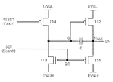
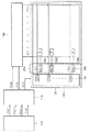
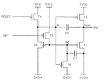
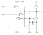
- ドレーン電極が第1エミッション電源と連結され、ゲート電極がQBノードと連結され、セット信号に対応して第1エミッション電源電圧をソース電極と連結された出力ノードに出力する第1トランジスター;
ソース電極が第2エミッション電源と連結され、ゲート電極がQノードと連結され、リセット信号に対応して第2エミッション電源電圧をドレーン電極と連結された前記出力ノードに出力する第2トランジスター;
ソース電極が第2ゲート電源と連結され、ドレーン電極が前記QBノードと連結され、前記セット信号に対応して第2ゲート電源電圧を前記QBノードに伝達する第3トランジスター;
ソース電極が前記QBノードと連結され、ゲート電極が前記Qノードと連結され、ドレーン電極が第1ゲート電源と連結され、前記リセット信号に対応して第1ゲート電源電圧を前記QBノードに伝達する第4トランジスター;及び
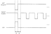
前記QBノード及び前記第1トランジスターのドレーン電極の間で連結される第1キャパシターを含む、有機発光ディスプレイ装置のエミッション信号制御回路。 - 前記セット信号によって前記第3トランジスターがターンオンされれば、前記第1トランジスターがターンオンされて前記第1エミッション電源電圧が前記出力ノードに出力され、前記第2ゲート電源電圧が前記第1キャパシターに貯蔵されることを特徴とする、請求項1に記載の有機発光ディスプレイ装置のエミッション信号制御回路。
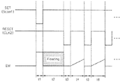
- 前記セット信号によって前記第3トランジスターがターンオフされれば、前記第1キャパシターに貯蔵された電圧によって前記第1トランジスターがターンオン状態を維持することを特徴とする、請求項2に記載の有機発光ディスプレイ装置のエミッション信号制御回路。
- 前記リセット信号によって前記第2トランジスターがターンオンされれば、前記第2エミッション電源電圧が前記出力ノードに出力され、前記第4トランジスターがターンオンされて前記第1ゲート電源によって前記第1トランジスターがターンオフ状態を維持することを特徴とする、請求項1に記載の有機発光ディスプレイ装置のエミッション信号制御回路。
- ソース電極が第2ゲート電源と連結され、ドレーン電極が前記Qノードと連結されて、前記リセット信号に対応して前記第2ゲート電源電圧を前記Qノードに伝達する第5トランジスターをさらに含むことを特徴とする、請求項1に記載の有機発光ディスプレイ装置のエミッション信号制御回路。
- 前記第1エミッション電源電圧の大きさと前記第1ゲート電源電圧の大きさは相異なるように設定されることを特徴とする、請求項1に記載の有機発光ディスプレイ装置のエミッション信号制御回路。
- セット信号を印加して第3トランジスター及び前記第3トランジスターとQBノードで連結される第1トランジスターをターンオンさせて出力ノードに第1エミッション電源電圧を出力する段階;
前記第3トランジスターをターンオフさせた後、前記第1トランジスター及び前記QBノードの間に連結される第1キャパシターに貯蔵された電圧を利用して前記出力ノードに第1エミッション電源電圧を出力する段階;及び
リセット信号を印加して第5トランジスター及び前記第5トランジスターとQノードで連結される第2トランジスターをターンオンさせて前記出力ノードに第2エミッション電源電圧を出力する段階を含む、有機発光ディスプレイ装置のエミッション信号制御方法。 - 前記第3トランジスターがターンオンされれば、前記第2ゲート電源電圧が前記第1キャパシターに貯蔵されることを特徴とする、請求項7に記載の有機発光ディスプレイ装置のエミッション信号制御方法。
- 前記第5トランジスターがターンオンドされれば、前記第5トランジスターと前記Qノードで連結される第4トランジスターがターンオンされ、前記第4トランジスターを通じて伝達される第1ゲート電源電圧によって前記第1トランジスターがターンオフ状態を維持することを特徴とする、請求項7に記載の有機発光ディスプレイ装置のエミッション信号制御方法。
- 前記第1エミッション電源電圧の大きさと前記第1ゲート電源電圧の大きさは相異なるように設定されることを特徴とする、請求項9に記載の有機発光ディスプレイ装置のエミッション信号制御方法。
- 複数の画素を含むパネル;
前記複数の画素それぞれにスキャン信号を供給するための複数のシフトレジスター;及び
前記複数のシフトレジスターと連結され、前記複数の画素それぞれにエミッション信号を供給するためのエミッション信号制御回路を含み、
前記エミッション信号制御回路は、
ドレーン電極が第1エミッション電源と連結され、ゲート電極がQBノードと連結されて、セット信号に対応して第1エミッション電源電圧をソース電極と連結された出力ノードに出力する第1トランジスター;
ソース電極が第2エミッション電源と連結され、ゲート電極がQノードと連結されて、リセット信号に対応して第2エミッション電源電圧をドレーン電極と連結された前記出力ノードに出力する第2トランジスター;
ソース電極が第2ゲート電源と連結され、ドレーン電極が前記QBノードと連結されて、前記セット信号に対応して第2ゲート電源電圧を前記QBノードに伝達する第3トランジスター;
ソース電極が前記QBノードと連結され、ゲート電極が前記Qノードと連結されて、ドレーン電極が第1ゲート電源と連結され、前記リセット信号に対応して第1ゲート電源電圧を前記QBノードに伝達する第4トランジスター;及び
前記QBノード及び前記第1トランジスターのドレーン電極の間に連結される第1キャパシターを含む、有機発光ディスプレイ装置。 - 前記セット信号によって前記第3トランジスターがターンオンされれば、前記第1トランジスターがターンオンされて前記第1エミッション電源電圧が前記出力ノードに出力され、前記第2ゲート電源電圧が前記第1キャパシターに貯蔵されることを特徴とする、請求項11に記載の有機発光ディスプレイ装置。
- 前記セット信号によって前記第3トランジスターがターンオフされれば、前記第1キャパシターに貯蔵された電圧によって前記第1トランジスターがターンオン状態を維持することを特徴とする、請求項12に記載の有機発光ディスプレイ装置。
- 前記リセット信号によって前記第2トランジスターがターンオンされれば、前記第2エミッション電源電圧が前記出力ノードに出力され、前記第4トランジスターがターンオンされ、前記第1ゲート電源によって前記第1トランジスターがターンオフ状態を維持することを特徴とする、請求項11に記載の有機発光ディスプレイ装置。
- 前記エミッション信号制御回路は、
ソース電極が第2ゲート電源と連結され、ドレーン電極が前記Qノードと連結されて、前記リセット信号に対応して前記第2ゲート電源電圧を前記Qノードに伝達する第5トランジスターをさらに含むことを特徴とする、請求項11に記載の有機発光ディスプレイ装置。 - 前記第1エミッション電源電圧の大きさと前記第1ゲート電源電圧の大きさは相異なるように設定されることを特徴とする、請求項11に記載の有機発光ディスプレイ装置。
Applications Claiming Priority (2)
| Application Number | Priority Date | Filing Date | Title |
|---|---|---|---|
| KR10-2015-0189223 | 2015-12-30 | ||
| KR1020150189223A KR102595497B1 (ko) | 2015-12-30 | 2015-12-30 | Em 신호 제어 회로, em 신호 제어 방법 및 유기 발광 표시 장치 |
Publications (2)
| Publication Number | Publication Date |
|---|---|
| JP2017120406A true JP2017120406A (ja) | 2017-07-06 |
| JP6539637B2 JP6539637B2 (ja) | 2019-07-03 |
Family
ID=57914651
Family Applications (1)
| Application Number | Title | Priority Date | Filing Date |
|---|---|---|---|
| JP2016243975A Active JP6539637B2 (ja) | 2015-12-30 | 2016-12-16 | 有機発光ディスプレイ装置のエミッション信号制御回路及びエミッション信号制御方法、並びに有機発光ディスプレイ装置 |
Country Status (5)
| Country | Link |
|---|---|
| US (1) | US10140921B2 (ja) |
| EP (1) | EP3188170B1 (ja) |
| JP (1) | JP6539637B2 (ja) |
| KR (1) | KR102595497B1 (ja) |
| CN (1) | CN107068067B (ja) |
Cited By (1)
| Publication number | Priority date | Publication date | Assignee | Title |
|---|---|---|---|---|
| JP2020021072A (ja) * | 2018-07-31 | 2020-02-06 | エルジー ディスプレイ カンパニー リミテッド | ゲート駆動部およびこれを用いた電界発光表示装置 |
Families Citing this family (3)
| Publication number | Priority date | Publication date | Assignee | Title |
|---|---|---|---|---|
| KR102721846B1 (ko) * | 2016-11-30 | 2024-10-24 | 엘지디스플레이 주식회사 | 표시 장치용 발광 제어부 및 이를 적용한 유기 발광 표시 장치 |
| CN114694553A (zh) * | 2020-12-28 | 2022-07-01 | 深圳市柔宇科技股份有限公司 | 发光扫描信号线驱动电路、显示面板及电子设备 |
| CN115132138B (zh) * | 2022-06-23 | 2025-01-07 | 合肥京东方卓印科技有限公司 | 发光控制单元及其控制方法、栅极驱动电路以及显示装置 |
Citations (6)
| Publication number | Priority date | Publication date | Assignee | Title |
|---|---|---|---|---|
| US20100188316A1 (en) * | 2009-01-29 | 2010-07-29 | Hwan-Soo Jang | Emission control driver and organic light emitting display device using the same |
| JP2011164606A (ja) * | 2010-02-05 | 2011-08-25 | Samsung Mobile Display Co Ltd | 表示装置及びその駆動方法 |
| US20120038609A1 (en) * | 2010-08-11 | 2012-02-16 | Samsung Mobile Display Co., Ltd. | Driver and Display Device Using the Same |
| JP2012189752A (ja) * | 2011-03-10 | 2012-10-04 | Japan Display East Co Ltd | 表示装置 |
| US20140204009A1 (en) * | 2013-01-23 | 2014-07-24 | Samsung Display Co., Ltd. | Gate driver and a display device including the same |
| US20150364079A1 (en) * | 2014-06-16 | 2015-12-17 | Boe Technology Group Co., Ltd. | Shift register unit, gate driving circuit and display panel |
Family Cites Families (10)
| Publication number | Priority date | Publication date | Assignee | Title |
|---|---|---|---|---|
| US4868427A (en) * | 1987-10-30 | 1989-09-19 | Gazelle Microcircuits, Inc. | ECL to TTL circuit |
| NL8800075A (nl) * | 1988-01-14 | 1989-08-01 | Philips Nv | Hot carrier stress vrije push-pull uitgangsschakeling. |
| US5304867A (en) * | 1991-12-12 | 1994-04-19 | At&T Bell Laboratories | CMOS input buffer with high speed and low power |
| KR101231846B1 (ko) | 2006-04-07 | 2013-02-08 | 엘지디스플레이 주식회사 | 유기발광다이오드 표시소자 및 그의 구동 방법 |
| KR20080114365A (ko) | 2007-06-27 | 2008-12-31 | 엘지디스플레이 주식회사 | 유기발광다이오드 표시장치 및 그 구동방법 |
| CN101783124B (zh) * | 2010-02-08 | 2013-05-08 | 北京大学深圳研究生院 | 栅极驱动电路单元、栅极驱动电路及显示装置 |
| KR101710661B1 (ko) * | 2010-04-29 | 2017-02-28 | 삼성디스플레이 주식회사 | 게이트 구동회로 및 이를 갖는 표시장치 |
| KR101725212B1 (ko) * | 2010-12-31 | 2017-04-10 | 엘지디스플레이 주식회사 | 에미션 구동장치 및 이를 이용한 유기발광다이오드 표시장치 |
| CN102708795B (zh) * | 2012-02-29 | 2014-11-12 | 京东方科技集团股份有限公司 | 阵列基板行驱动单元、阵列基板行驱动电路以及显示装置 |
| KR102117987B1 (ko) * | 2014-02-24 | 2020-06-10 | 삼성디스플레이 주식회사 | 유기전계발광 표시장치 |
-
2015
- 2015-12-30 KR KR1020150189223A patent/KR102595497B1/ko active Active
-
2016
- 2016-12-06 CN CN201611107581.4A patent/CN107068067B/zh active Active
- 2016-12-12 US US15/376,059 patent/US10140921B2/en active Active
- 2016-12-16 JP JP2016243975A patent/JP6539637B2/ja active Active
- 2016-12-23 EP EP16206715.1A patent/EP3188170B1/en active Active
Patent Citations (6)
| Publication number | Priority date | Publication date | Assignee | Title |
|---|---|---|---|---|
| US20100188316A1 (en) * | 2009-01-29 | 2010-07-29 | Hwan-Soo Jang | Emission control driver and organic light emitting display device using the same |
| JP2011164606A (ja) * | 2010-02-05 | 2011-08-25 | Samsung Mobile Display Co Ltd | 表示装置及びその駆動方法 |
| US20120038609A1 (en) * | 2010-08-11 | 2012-02-16 | Samsung Mobile Display Co., Ltd. | Driver and Display Device Using the Same |
| JP2012189752A (ja) * | 2011-03-10 | 2012-10-04 | Japan Display East Co Ltd | 表示装置 |
| US20140204009A1 (en) * | 2013-01-23 | 2014-07-24 | Samsung Display Co., Ltd. | Gate driver and a display device including the same |
| US20150364079A1 (en) * | 2014-06-16 | 2015-12-17 | Boe Technology Group Co., Ltd. | Shift register unit, gate driving circuit and display panel |
Cited By (6)
| Publication number | Priority date | Publication date | Assignee | Title |
|---|---|---|---|---|
| JP2020021072A (ja) * | 2018-07-31 | 2020-02-06 | エルジー ディスプレイ カンパニー リミテッド | ゲート駆動部およびこれを用いた電界発光表示装置 |
| KR20200013923A (ko) * | 2018-07-31 | 2020-02-10 | 엘지디스플레이 주식회사 | 게이트 구동부 및 이를 이용한 전계발광 표시장치 |
| US11270629B2 (en) | 2018-07-31 | 2022-03-08 | Lg Display Co., Ltd. | Gate driver and electroluminescence display device using the same |
| JP7071318B2 (ja) | 2018-07-31 | 2022-05-18 | エルジー ディスプレイ カンパニー リミテッド | ゲート駆動部およびこれを用いた電界発光表示装置 |
| US11545080B2 (en) | 2018-07-31 | 2023-01-03 | Lg Display Co., Ltd. | Gate driver and electroluminescence display device using the same |
| KR102733928B1 (ko) | 2018-07-31 | 2024-11-22 | 엘지디스플레이 주식회사 | 게이트 구동부 및 이를 이용한 전계발광 표시장치 |
Also Published As
| Publication number | Publication date |
|---|---|
| JP6539637B2 (ja) | 2019-07-03 |
| CN107068067B (zh) | 2019-11-12 |
| KR102595497B1 (ko) | 2023-10-30 |
| EP3188170B1 (en) | 2020-10-28 |
| KR20170080736A (ko) | 2017-07-11 |
| EP3188170A1 (en) | 2017-07-05 |
| US10140921B2 (en) | 2018-11-27 |
| CN107068067A (zh) | 2017-08-18 |
| US20170193911A1 (en) | 2017-07-06 |
Similar Documents
| Publication | Publication Date | Title |
|---|---|---|
| TWI767461B (zh) | 閘極驅動電路以及使用其的顯示裝置 | |
| US9454935B2 (en) | Organic light emitting diode display device | |
| KR20210083644A (ko) | 유기발광 표시장치 및 그 구동방법 | |
| KR102753014B1 (ko) | 게이트 구동회로 및 이를 이용한 표시장치 | |
| US8941629B2 (en) | Scan driver and organic light emitting display device using the same | |
| KR102582032B1 (ko) | 발광 구동부 및 이를 포함하는 표시 장치 | |
| US9583065B2 (en) | Gate driver and display device having the same | |
| KR20190020549A (ko) | 게이트 구동회로 및 이를 이용한 표시장치와 그 구동 방법 | |
| JP2019032519A (ja) | ゲート駆動部及びこれを備えた平面表示装置 | |
| WO2018129932A1 (zh) | 移位寄存器单元电路及其驱动方法、栅极驱动电路和显示装置 | |
| EP3316242A1 (en) | Organic light emitting display and apparatus for driving same | |
| EP3330958B1 (en) | Display device having an integrated type scan driver | |
| KR20190018982A (ko) | 게이트 구동회로와 이를 이용한 표시장치 | |
| KR20220093764A (ko) | 게이트 구동 회로 및 이를 이용한 유기 발광 표시 장치 | |
| CN109727580B (zh) | 显示面板 | |
| KR20190032959A (ko) | 시프트레지스터 및 이를 포함하는 유기발광 표시장치 | |
| CN114822383A (zh) | 显示面板及显示装置 | |
| KR20190031026A (ko) | 시프트레지스터 및 이를 포함하는 표시장치 | |
| KR20190040849A (ko) | 유기 발광 표시 장치 및 그의 구동 방법 | |
| KR20210080960A (ko) | 게이트 구동 회로 및 이를 포함하는 발광 표시 장치 | |
| CN113096606A (zh) | Goa电路、显示面板及电子装置 | |
| JP6539637B2 (ja) | 有機発光ディスプレイ装置のエミッション信号制御回路及びエミッション信号制御方法、並びに有機発光ディスプレイ装置 | |
| KR102051389B1 (ko) | 액정표시장치 및 이의 구동회로 | |
| KR20150066981A (ko) | 표시장치 | |
| KR102436560B1 (ko) | 게이트 구동회로 및 이를 이용한 유기발광 표시장치 |
Legal Events
| Date | Code | Title | Description |
|---|---|---|---|
| A977 | Report on retrieval |
Free format text: JAPANESE INTERMEDIATE CODE: A971007 Effective date: 20171016 |
|
| A131 | Notification of reasons for refusal |
Free format text: JAPANESE INTERMEDIATE CODE: A131 Effective date: 20171031 |
|
| A601 | Written request for extension of time |
Free format text: JAPANESE INTERMEDIATE CODE: A601 Effective date: 20180131 |
|
| A521 | Request for written amendment filed |
Free format text: JAPANESE INTERMEDIATE CODE: A523 Effective date: 20180402 |
|
| RD02 | Notification of acceptance of power of attorney |
Free format text: JAPANESE INTERMEDIATE CODE: A7422 Effective date: 20180531 |
|
| RD04 | Notification of resignation of power of attorney |
Free format text: JAPANESE INTERMEDIATE CODE: A7424 Effective date: 20180612 |
|
| RD04 | Notification of resignation of power of attorney |
Free format text: JAPANESE INTERMEDIATE CODE: A7424 Effective date: 20180704 |
|
| A131 | Notification of reasons for refusal |
Free format text: JAPANESE INTERMEDIATE CODE: A131 Effective date: 20181002 |
|
| A521 | Request for written amendment filed |
Free format text: JAPANESE INTERMEDIATE CODE: A523 Effective date: 20181217 |
|
| TRDD | Decision of grant or rejection written | ||
| A01 | Written decision to grant a patent or to grant a registration (utility model) |
Free format text: JAPANESE INTERMEDIATE CODE: A01 Effective date: 20190521 |
|
| A61 | First payment of annual fees (during grant procedure) |
Free format text: JAPANESE INTERMEDIATE CODE: A61 Effective date: 20190610 |
|
| R150 | Certificate of patent or registration of utility model |
Ref document number: 6539637 Country of ref document: JP Free format text: JAPANESE INTERMEDIATE CODE: R150 |
|
| R250 | Receipt of annual fees |
Free format text: JAPANESE INTERMEDIATE CODE: R250 |
|
| R250 | Receipt of annual fees |
Free format text: JAPANESE INTERMEDIATE CODE: R250 |
|
| R250 | Receipt of annual fees |
Free format text: JAPANESE INTERMEDIATE CODE: R250 |
|
| R250 | Receipt of annual fees |
Free format text: JAPANESE INTERMEDIATE CODE: R250 |
|
| R250 | Receipt of annual fees |
Free format text: JAPANESE INTERMEDIATE CODE: R250 |