JP2017120879A - Protection element, manufacturing method of protection element, mounting substrate, and electronic device - Google Patents
Protection element, manufacturing method of protection element, mounting substrate, and electronic device Download PDFInfo
- Publication number
- JP2017120879A JP2017120879A JP2016176807A JP2016176807A JP2017120879A JP 2017120879 A JP2017120879 A JP 2017120879A JP 2016176807 A JP2016176807 A JP 2016176807A JP 2016176807 A JP2016176807 A JP 2016176807A JP 2017120879 A JP2017120879 A JP 2017120879A
- Authority
- JP
- Japan
- Prior art keywords
- resin
- protective element
- semiconductor ceramic
- protection element
- ceramic particles
- Prior art date
- Legal status (The legal status is an assumption and is not a legal conclusion. Google has not performed a legal analysis and makes no representation as to the accuracy of the status listed.)
- Pending
Links
Images






Landscapes
- Compositions Of Macromolecular Compounds (AREA)
- Thermistors And Varistors (AREA)
- Coils Or Transformers For Communication (AREA)
- Non-Metallic Protective Coatings For Printed Circuits (AREA)
Abstract
Description
本発明は、保護素子、保護素子の製造方法、実装基板および電子機器に関するものである。 The present invention relates to a protective element, a method for manufacturing the protective element, a mounting substrate, and an electronic device.
近年、電子機器の小型化、薄型化が急速に進んでおり、それに伴って、配線基板に実装される電子部品の密度や、配線基板に敷設される配線の密度も高くなっている。 In recent years, electronic devices have been rapidly reduced in size and thickness, and accordingly, the density of electronic components mounted on the wiring board and the density of wiring laid on the wiring board have also increased.
このような高密度化が進行すると、静電気による過電圧が回路に重畳したとき、電子部品の破壊や誤作動が起こり易くなる。特に、モバイル機器のように人体に触れた状態で使用されたり、電子機器同士をケーブルで接続したりする機会が増えると、電子機器が静電気に曝される機会も増加するため、このような不具合が発生する確率は高くなる。 When such high density progresses, when an overvoltage caused by static electricity is superimposed on the circuit, the electronic components are easily broken or malfunctioned. This is especially true when there is an increased opportunity for electronic devices to be exposed to static electricity when they are used in contact with a human body, such as mobile devices, or when electronic devices are connected with cables. The probability of occurrence is high.
そこで、過電圧から回路を保護するため、半導体セラミックスを用いたバリスタが提案されている。例えば、特許文献1には、積層チップバリスタを組み込むことにより、ICカードに内蔵されている半導体集積回路チップを静電破壊から防止することが開示されている。 Therefore, varistors using semiconductor ceramics have been proposed to protect the circuit from overvoltage. For example, Patent Document 1 discloses that a semiconductor integrated circuit chip built in an IC card is prevented from electrostatic breakdown by incorporating a multilayer chip varistor.
しかしながら、電子機器に対する小型化、薄型化のさらなる要請は、小型の積層チップバリスタを配置する余地さえ奪いつつある。このため、静電放電による過電圧から回路を保護しつつ、空間占有率の極めて小さい保護素子の開発が急務になっている。また、併せて、わずかな余剰空間にも配置可能な自由度の高さも、保護素子に対する要請の1つである。 However, further demands for downsizing and thinning of electronic devices are taking away even room for arranging small multilayer chip varistors. For this reason, there is an urgent need to develop a protective element with a very small space occupancy while protecting a circuit from an overvoltage caused by electrostatic discharge. In addition, a high degree of freedom that can be arranged in a small excess space is one of the requirements for the protection element.
本発明の目的は、空間占有率が小さく配置自由度が高い保護素子、かかる保護素子を効率よく製造可能な保護素子の製造方法、前記保護素子を備え搭載されている電子部品を過電圧から保護し得る実装基板、および、小型で信頼性の高い電子機器を提供することにある。 An object of the present invention is to provide a protective element having a small space occupancy ratio and a high degree of freedom in arrangement, a method for manufacturing a protective element capable of efficiently manufacturing such a protective element, and protecting an electronic component equipped with the protective element from overvoltage. An object of the present invention is to provide a mounting board and a small and highly reliable electronic device.
このような目的は、下記(1)〜(11)の本発明により達成される。
(1) 基部の表面上において互いに離間する導電部同士を跨いで設けられ、電圧−電流特性がオームの法則に従わない非直線性を示す保護素子であって、
粒界部と前記粒界部によって離隔される複数の結晶部とを含む半導体セラミックス粒子と、比誘電率4以下の樹脂の硬化物と、を有し、
前記半導体セラミックス粒子が前記基部側に偏在していることを特徴とする保護素子。
Such an object is achieved by the present inventions (1) to (11) below.
(1) A protective element that is provided across the conductive parts that are spaced apart from each other on the surface of the base, and that exhibits non-linearity in which the voltage-current characteristics do not follow Ohm's law,
A semiconductor ceramic particle including a grain boundary part and a plurality of crystal parts separated by the grain boundary part, and a cured product of a resin having a relative dielectric constant of 4 or less,
A protective element, wherein the semiconductor ceramic particles are unevenly distributed on the base side.
(2) 基部の表面上において互いに離間する導電部同士を跨いで設けられ、電圧−電流特性がオームの法則に従わない非直線性を示す保護素子であって、
粒界部と前記粒界部によって離隔される複数の結晶部とを含む半導体セラミックス粒子と、硬化性の樹脂の硬化物と、を有し、
前記半導体セラミックス粒子が前記基部側に偏在していることを特徴とする保護素子。
(2) A protective element that is provided across the conductive parts that are spaced apart from each other on the surface of the base, and exhibits non-linearity in which the voltage-current characteristics do not follow Ohm's law,
Semiconductor ceramic particles including a grain boundary part and a plurality of crystal parts separated by the grain boundary part, and a cured product of a curable resin,
A protective element, wherein the semiconductor ceramic particles are unevenly distributed on the base side.
(3) 当該保護素子のうち、前記基部側における前記半導体セラミックス粒子の体積分率を1としたとき、前記基部とは反対側における前記半導体セラミックス粒子の体積分率は、0以上0.90以下である上記(1)または(2)に記載の保護素子。 (3) Among the protective elements, when the volume fraction of the semiconductor ceramic particles on the base side is 1, the volume fraction of the semiconductor ceramic particles on the side opposite to the base is 0 or more and 0.90 or less. The protective element according to (1) or (2) above.
(4) 前記樹脂は、エポキシ系樹脂、シリコーン系樹脂、オレフィン系樹脂またはベンゾシクロブテン系樹脂を含む上記(1)ないし(3)のいずれかに記載の保護素子。 (4) The protective element according to any one of (1) to (3), wherein the resin includes an epoxy resin, a silicone resin, an olefin resin, or a benzocyclobutene resin.
(5) 前記保護素子の表面は、少なくとも一部に湾曲凸面を含んでいる上記(1)ないし(4)のいずれかに記載の保護素子。 (5) The protective element according to any one of (1) to (4), wherein the surface of the protective element includes a curved convex surface at least partially.
(6) 粒界部と前記粒界部によって離隔される複数の結晶部とを含む半導体セラミックス粒子と、未硬化の硬化性樹脂と、を含む組成物を塗布する工程と、
前記組成物中の前記硬化性樹脂を硬化させることにより、電圧−電流特性がオームの法則に従わない非直線性を示す保護素子を形成する工程と、
を有することを特徴とする保護素子の製造方法。
(6) applying a composition comprising semiconductor ceramic particles including a grain boundary part and a plurality of crystal parts separated by the grain boundary part, and an uncured curable resin;
Curing the curable resin in the composition to form a protective element exhibiting non-linearity in which voltage-current characteristics do not follow Ohm's law;
The manufacturing method of the protection element characterized by having.
(7) 前記組成物を塗布する工程の前に設けられ、基部と、前記基部の表面上に設けられ互いに離間する複数の導電部と、前記導電部と電気的に接続されている電子部品と、が配置されている絶縁部材を用意する工程をさらに有し、
前記組成物を塗布する工程において、前記導電部同士を跨ぐ領域に前記組成物を塗布する上記(6)に記載の保護素子の製造方法。
(7) provided before the step of applying the composition, a base, a plurality of conductive parts provided on the surface of the base and spaced apart from each other, and an electronic component electrically connected to the conductive part The method further comprises the step of preparing an insulating member in which is disposed,
The method for manufacturing a protective element according to (6), wherein in the step of applying the composition, the composition is applied to a region straddling the conductive portions.
(8) 前記領域に向けて前記組成物を吐出することにより、前記組成物を塗布する上記(7)に記載の保護素子の製造方法。 (8) The method for manufacturing a protective element according to (7), wherein the composition is applied by discharging the composition toward the region.
(9) 基部と、
前記基部の表面上に設けられ、互いに離間する複数の導電部と、
前記導電部と電気的に接続されている電子部品と、
前記導電部同士を跨いで設けられ、粒界部と前記粒界部によって離隔される複数の結晶部とを含む半導体セラミックス粒子と、硬化性樹脂の硬化物と、を含み、電圧−電流特性がオームの法則に従わない非直線性を示す保護素子と、
を有し、
前記保護素子において前記半導体セラミックス粒子が前記基部側に偏在していることを特徴とする実装基板。
(9) the base,
A plurality of conductive portions provided on the surface of the base and spaced apart from each other;
An electronic component electrically connected to the conductive portion;
The semiconductor ceramic particles, which are provided across the conductive parts and include a grain boundary part and a plurality of crystal parts separated by the grain boundary part, and a cured product of a curable resin, have a voltage-current characteristic. A protective element exhibiting non-linearity that does not follow Ohm's law;
Have
In the protective element, the semiconductor ceramic particles are unevenly distributed on the base side.
(10) さらに、前記導電部の表面上の一部を覆うよう設けられ、前記導電部同士の間隙を含む領域に対応する開口を備えるソルダーレジスト膜を有し、
前記保護素子は、前記開口から前記ソルダーレジスト膜の表面上にはみ出すように設けられている上記(9)に記載の実装基板。
(10) Further, a solder resist film is provided so as to cover a part on the surface of the conductive portion, and has an opening corresponding to a region including a gap between the conductive portions,
The mounting substrate according to (9), wherein the protection element is provided so as to protrude from the opening onto the surface of the solder resist film.
(11) 上記(1)ないし(5)のいずれかに記載の保護素子を備えることを特徴とする電子機器。 (11) An electronic device comprising the protective element according to any one of (1) to (5) above.
本発明によれば、空間占有率が小さく配置自由度が高い保護素子が得られる。
また、本発明によれば、前記保護素子を効率よく製造することができる。
According to the present invention, a protection element having a small space occupancy and a high degree of freedom in arrangement can be obtained.
Moreover, according to this invention, the said protection element can be manufactured efficiently.
また、本発明によれば、前記保護素子を備え搭載されている電子部品を過電圧から保護し得る実装基板が得られる。
また、本発明によれば、小型で信頼性が高い電子機器が得られる。
In addition, according to the present invention, it is possible to obtain a mounting substrate that can protect an electronic component equipped with the protection element from overvoltage.
In addition, according to the present invention, a small and highly reliable electronic device can be obtained.
以下、本発明の保護素子、保護素子の製造方法、実装基板および電子機器について添付図面に示す好適実施形態に基づいて詳細に説明する。 Hereinafter, a protection element, a manufacturing method of a protection element, a mounting substrate, and an electronic device according to the present invention will be described in detail based on preferred embodiments shown in the accompanying drawings.
<実装基板>
≪第1実施形態≫
まず、本発明の実装基板の第1実施形態およびそれに含まれる本発明の保護素子の第1実施形態について説明する。
<Mounting board>
<< First Embodiment >>
First, a first embodiment of a mounting board of the present invention and a first embodiment of a protection element of the present invention included therein will be described.
図1は、本発明の実装基板の第1実施形態が備える電気回路の一例を示す回路図である。また、図2は、図1に示す電気回路を構成する電気配線近傍を拡大して示す斜視図である。 FIG. 1 is a circuit diagram showing an example of an electric circuit provided in the first embodiment of the mounting board of the present invention. FIG. 2 is an enlarged perspective view showing the vicinity of the electric wiring constituting the electric circuit shown in FIG.
図1に示す実装基板1は、絶縁基板2(基部)と、絶縁基板2の表面上に設けられ互いに離間している2本の配線31、32(導電部)と、配線31、32と電気的に接続されている被保護回路4(電子部品)と、配線31と配線32とを跨いで設けられている保護素子5と、を有している。これらの配線31、32と被保護回路4と保護素子5とにより、電気回路が構成されている。また、実装基板1には、電源6が配線31および配線32と電気的に接続されており、それらの間に電圧を印加し得るようになっている。
以下、各部の構成について順次詳述する。
The mounting substrate 1 shown in FIG. 1 includes an insulating substrate 2 (base portion), two
Hereinafter, the configuration of each unit will be described in detail.
絶縁基板2は、配線31、32や被保護回路4、保護素子5等を支持する基板である。
絶縁基板2の構成材料としては、絶縁性を有する材料であれば特に限定されないが、例えば、ポリイミド系樹脂、ポリアミド系樹脂、エポキシ系樹脂、各種ビニル系樹脂、ポリエーテルスルホン系樹脂、シクロオレフィン系樹脂、ポリカーボネート系樹脂、ポリエチレンテレフタレート樹脂やポリエチレンナフタレートのようなポリエステル系樹脂等の各種樹脂材料(フレキシブルプリント配線板用樹脂材料)が挙げられる。
The insulating
The constituent material of the insulating
この他、絶縁基板2の構成材料としては、例えば、紙、ガラス布、樹脂フィルム等を基材とし、この基材に、フェノール系樹脂、ポリエステル系樹脂、エポキシ系樹脂、シアネート樹脂、ポリイミド系樹脂、フッ素系樹脂等の樹脂材料を含浸させたもの、具体的には、ガラス布・エポキシ銅張積層板、ガラス不織布・エポキシ銅張積層板等のコンポジット銅張積層板に使用される絶縁性基板の他、ポリエーテルイミド樹脂基板、ポリエーテルケトン樹脂基板、ポリサルフォン系樹脂基板等の耐熱・熱可塑性の有機系リジッド基板や、アルミナ基板、窒化アルミニウム基板、炭化ケイ素基板等のセラミックス系リジッド基板等が挙げられる。
In addition, as a constituent material of the insulating
配線31、32は、絶縁基板2の表面上に設けられた導電層で構成されている。
配線31、32の構成材料としては、例えば、銅、アルミニウム、ニッケル、クロム、亜鉛、錫、金、銀等の金属単体、またはこれらの金属元素を含む合金といった金属材料が挙げられる。
The
Examples of the constituent material of the
また、配線31、32の形成方法としては、例えば、金属箔を貼り付ける方法、金属ペーストを焼き付ける方法、気相成膜法により成膜する方法、電解または無電解めっき法により成膜する方法等が挙げられる。また、このような方法で形成された金属層をパターニングする方法によっても形成することができる。
The
なお、図1に示す配線31、32の形態は、一例であり、さらに別の配線が設けられていてもよく、途中で分岐したりしていてもよい。
Note that the form of the
また、図1に示すラインインピーダンスZ0は、電源6の内部抵抗や実装基板1のラインインピーダンスに相当する抵抗成分を、抵抗素子に模して示したものである。
Further, the line impedance Z 0 shown in FIG. 1 is a resistance element corresponding to the internal resistance of the
被保護回路4は、保護素子5によって過電圧による損傷から保護される対象となる回路である。被保護回路4は、トランジスターや発光ダイオードのような素子を含むディスクリート回路であってもよく、IC(Integrated Circuit)やLSI(Large-Scale Integration)、半導体メモリーのような素子を含む集積回路であってもよく、これらを組み合わせた回路であってもよい。
The protected
なお、被保護回路4は、互いに離間する配線31および配線32と電気的に接続されている。これらの配線31、32を介して、被保護回路4に駆動電圧を印加したり、電気信号を送受信したりすることができる。
The protected
電源6は、配線31および配線32と電気的に接続されており、それらの間に電圧を印加する。これにより、被保護回路4を作動させることができる。
The
保護素子5は、互いに離間する配線31と配線32とを跨ぐように設けられている。保護素子5は、図2に示すように、絶縁基板2の表面や配線31、32の表面に沿う形状を有するとともに、これらの表面に密着している。これにより、保護素子5は、配線31および配線32と電気的に接続されているとともに、絶縁基板2に対して機械的に固定されている。
The
保護素子5は、電圧−電流特性がオームの法則に従わない非直線性を示す。なお、本明細書では、「電圧−電流特性がオームの法則に従わない非直線性」のことを「バリスタ特性」ともいう。
The
このようなバリスタ特性は、保護素子5を含む回路に所定電圧(保護素子5のバリスタ電圧)以下の電圧が印加されている間は絶縁性を示し、所定電圧を超える電圧が印加されたときには導電性を示す特性である。配線31と配線32との間に前述した所定電圧を超えるような高電圧が誘導された場合、かかるバリスタ特性により、導電性を示す保護素子5にサージ電流が流れる。これにより、被保護回路4に所定電圧を超える電圧が印加されるのを抑制することができる。
Such a varistor characteristic exhibits insulation while a voltage equal to or lower than a predetermined voltage (varistor voltage of the protective element 5) is applied to a circuit including the
そして、被保護回路4に対する高電圧の印加が防止されることにより、被保護回路4の損傷や劣化が抑制される。その結果、実装基板1の信頼性をより高めることができる。
Further, by preventing application of a high voltage to the protected
また、保護素子5の形状は、前述したように、配線31と配線32とを跨ぐ形状であれば特に限定されないものの、好ましくは表面の少なくとも一部に湾曲凸面が含まれた形状とされる。このような形状であれば、例えば保護素子5に負荷が加わったときでも、応力を局所的に集中させ難くなる。このため、保護素子5は、耐クラック性を有するものとなる。加えて、応力の集中に伴う剥離が起き難くなるため、保護素子5は、絶縁基板2や配線31、32に対する密着性にも優れたものとなる。
In addition, as described above, the shape of the
また、保護素子5の厚さは、特に限定されないが、半導体セラミックス粒子51の粒子径より厚いのが好ましい。これにより、保護素子5において半導体セラミックス粒子51が脱落し難くなり、保護素子5の信頼性をより高めることができる。
Further, the thickness of the
具体的には、保護素子5の最大厚さは、半導体セラミックス粒子51の平均粒子径D50の1.1〜1000倍程度であるのが好ましく、3.0〜500倍程度であるのがより好ましい。これにより、上記効果がより顕著になる。
Specifically, the maximum thickness of the
さらに、保護素子5の厚さは、配線31、32の厚さより厚いのが好ましい。これにより、保護素子5が配線31、32を包み込むことになるので、保護素子5と配線31、32との密着性がより高くなる。その結果、実装基板1の信頼性をより高めることができる。
Further, the thickness of the
ここで、配線31、32の他の構成例について説明する。
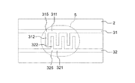
図3は、図1に示す電気回路を構成する電気配線の他の構成例を示す上面図である。なお、図3では、説明の便宜上、保護素子5の輪郭を破線で示し、保護素子5の陰に隠れている配線31、32の形状を実線で示している。
Here, another configuration example of the
FIG. 3 is a top view illustrating another configuration example of the electrical wiring configuring the electrical circuit illustrated in FIG. 1. In FIG. 3, for convenience of explanation, the outline of the
図3に示す配線31は、途中で2つに分岐する分岐点315を複数個有している。各分岐点315では、それぞれ、配線31が幹線311と支線312とに分岐している。
The
また、図3に示す配線32も、途中で2つに分岐する分岐点325を複数個有している。各分岐点325では、それぞれ、配線32が幹線321と支線322とに分岐している。
The
そして、幹線311および幹線321は、図2における配線31と配線32との関係と同様、互いに平行である。
The
一方、支線312は、その延在方向が幹線311と直交している。そして、支線312は、配線32側を指向して延在し、配線32に達する手前まで延びている。
On the other hand, the extending direction of the
また、支線322も、その延在方向が幹線321と直交している。そして、支線322も、配線31側を指向して延在し、配線31に達する手前まで延びている。
Further, the extending direction of the
さらに、支線312および支線322は、配線31、32の延在方向において交互に配置されている。これにより、配線31および配線32は、それぞれ平面視形状が櫛歯状をなすものとなる。
Further, the
その上で、図3に示す保護素子5は、複数の支線312や支線322を包含する位置に設けられている。これにより、図3に示す実装基板1では、配線31と配線32とが互いに離間しつつ対向している面積を、より大きく確保することができる。このため、より大きな面積において、保護素子5を配線31と配線32との間に介挿することができ、バリスタ特性を発現させられる面積の拡大を図ることができる。その結果、エネルギー耐量の増大といったバリスタ特性のさらなる向上を図ることができる。また、バリスタ特性を低下させることなく、保護素子5が占める面積の縮小を図ることができるので、高密度配線への適合性を高めることができる。
3 is provided at a position including a plurality of
なお、配線31に設けられる分岐点315の数は、特に限定されず、1個であってもよいが、好ましくは複数(例えば2〜100個程度)とされる。
The number of branch points 315 provided in the
同様に、配線32に設けられる分岐点325の数も、特に限定されず、1個であってもよいが、好ましくは複数(例えば2〜100個程度)とされる。
Similarly, the number of branch points 325 provided in the
また、配線31と配線32とに跨る保護素子5は、1個であっても、複数個であってもよい。
Moreover, the
ところで、このような保護素子5は、半導体セラミックス粒子51と、樹脂の硬化物52と、を含む。
By the way, such a
(半導体セラミックス粒子)
図4は、図2のA−A線断面図であり、図5は、図4に示す半導体セラミックス粒子の部分拡大図である。
(Semiconductor ceramic particles)
4 is a cross-sectional view taken along the line AA in FIG. 2, and FIG. 5 is a partially enlarged view of the semiconductor ceramic particles shown in FIG.
図5に示す半導体セラミックス粒子51は、粒界部511と、上記粒界部511によって離隔された複数の結晶部512とを有する粒子である。すなわち、半導体セラミックス粒子51は、結晶部512同士が粒界部511を介して凝集してなる二次粒子である。このような半導体セラミックス粒子51は、バリスタ電圧未満の電圧が印加された場合には、粒界部511が抵抗として作用するため電流を通さないが、バリスタ電圧以上の電圧が印加された場合には、トンネル効果が生じて図5に示す矢印のように電流を通すという特性を有する。
The
半導体セラミックス粒子51の平均粒子径D50は、例えば0.01μm以上1500μm以下であるのが好ましく、0.1μm以上1000μm以下であるのがより好ましく、1μm以上500μm以下であるのがさらに好ましく、5μm以上150μm以下であるのが特に好ましい。これにより、保護素子5の形状に依存することなく、バリスタ特性を発現させることが可能となる。
The average particle diameter D50 of the
また、半導体セラミックス粒子51は、球状粒子であることが好ましい。これにより、バリスタ特性の制御を容易に行うことができる。
The
半導体セラミックス粒子51において結晶部512は、酸化亜鉛、炭化ケイ素、チタン酸ストロンチウムおよびチタン酸バリウムからなる群より選択される1種以上を含む材料により形成されていることが好ましい。特に酸化亜鉛を主成分として含む材料は、半導体セラミックス粒子51自体の非直線性係数やエネルギー耐量を向上させる観点から好ましい。炭化ケイ素を主成分として含む材料は、絶縁破壊電圧が高いため、バリスタ電圧を高電圧に設定する場合には好適である。また、チタン酸ストロンチウムを主成分として含む材料は、高電圧・高周波ノイズの吸収や抑制という点において、好適である。
In the
半導体セラミックス粒子51において粒界部511は、ビスマス、プラセオジム、アンチモン、マンガン、コバルトおよびニッケル、またはこれらの化合物からなる群より選択される1種以上を含む材料により形成されていることが好ましい。中でも、粒界部511は、非直線性抵抗特性が良好であるという観点から、ビスマス、プラセオジム、またはこれらの化合物からなる群より選択される1種以上を含む材料により形成されていることが好ましい。なお、上述したこれらの化合物としては、酸化物、窒化物、有機化合物、その他の無機化合物等の形態が挙げられるが、バリスタ特性を良好に発現させる観点から、酸化物であることが好ましい。
In the
半導体セラミックス粒子51の含有量は、保護素子5のバリスタ特性をより確実に発現させるという観点から、保護素子5の全量において、好ましくは20質量%以上90質量%以下とされ、より好ましくは25質量%以上80質量%以下とされ、さらに好ましくは30質量%以上70質量%以下とされる。半導体セラミックス粒子51の含有量が前記範囲内となるよう制御することにより、図4に示す模式図のように、互いに隣り合う配線31と配線32との間隙が、半導体セラミックス粒子51によって埋められ易くなる。これにより、保護素子5のエネルギー耐量をより高めることができる。
The content of the
また、このとき、半導体セラミックス粒子51同士は互いに接しているのが好ましい。なお、半導体セラミックス粒子51の含有量を前記範囲内となるよう制御することにより、半導体セラミックス粒子51同士を互いに接し易くさせ、保護素子5のバリスタ特性をより確実に発現させることができる。
At this time, the
さらに、このような保護素子5は、半導体セラミックス粒子51と、未硬化の樹脂と、を含む組成物を、任意の箇所に塗布し、その後、樹脂を硬化させることによって容易に製造することが可能である。このため、図2に示す配線31、32のように、電気的に独立した2つの導電部が隣り合っている場合、それらを跨ぐように組成物を塗布し、その後、硬化処理を施すのみで、簡単に保護素子5を形成することができる。したがって、保護素子5は、空間占有率が小さく配置自由度が高いものとなる。その結果、実装基板1は、例えばディスクリート部品(バリスタ素子)を採用する場合に比べて、部材調達コストの削減が図られるとともに、製造コストの削減も図ることができる。
Furthermore, such a
なお、チップバリスタ素子のようなディスクリート部品を搭載する場合、はんだ付けを要するためにチップバリスタ素子に対してはんだリフロー処理を施す必要がある。このため、絶縁基板2には、はんだの融点を超える耐熱温度(例えば260℃前後)が要求される。
When a discrete component such as a chip varistor element is mounted, since soldering is required, it is necessary to perform a solder reflow process on the chip varistor element. For this reason, the insulating
これに対し、本発明では、前述したように組成物を任意の箇所に塗布した後、樹脂を硬化させることによって保護素子5を製造することが可能である。このため、製造に要する温度は、50〜200℃程度であり、絶縁基板2に求められる耐熱温度を低くすることが可能である。
On the other hand, in this invention, after apply | coating a composition to arbitrary places as mentioned above, it is possible to manufacture the
なお、「配線31と配線32とを跨ぐように」とは、1つの保護素子5が、配線31と配線32の双方に接触しており、かつ、双方と電気的に接続されている状態を指す。したがって、保護素子5の平面視形状や厚さ等は、特に限定されない。
Note that “so as to straddle the
ここで、半導体セラミックス粒子51は、絶縁基板2(基部)側に偏在している。すなわち、本実施形態では、図4に示すように、保護素子5の断面の下方(絶縁基板2側)においては半導体セラミックス粒子51の占有率が高くなっている一方、上方(絶縁基板2とは反対側)においては樹脂の硬化物52の占有率が高くなっている。
Here, the
このような保護素子5では、絶縁基板2側、すなわち、配線31、32側に半導体セラミックス粒子51が集積することになる。このため、配線31と配線32との間に半導体セラミックス粒子51が高密度に配置されることとなり、バリスタ特性が特に良好な保護素子5が得られる。よって、かかる保護素子5を含む実装基板1は、被保護回路4に印加される過電圧を良好に緩和可能なものとなる。
In such a
また、半導体セラミックス粒子51が絶縁基板2側に偏在する分、保護素子5のバリスタ特性を著しく損なうことなく、保護素子5全体における半導体セラミックス粒子51の比率を低くし、反対に、樹脂の硬化物52の比率を高めることができる。すなわち、半導体セラミックス粒子51のうち、バリスタ特性の発現に寄与しているのは、配線31と配線32との間に位置する粒子であるため、それ以外の部位に存在する粒子は、バリスタ特性の発現に直接寄与し難い。したがって、半導体セラミックス粒子51を偏在させることによって、バリスタ特性を損なうことなく、樹脂の硬化物52の比率を高めることが可能である。
In addition, since the
このようにして樹脂の硬化物52の比率を高めることにより、保護素子5の信頼性を高めることができる。すなわち、保護素子5は、樹脂の硬化物52の比率が高くなることで、半導体セラミックス粒子51同士を結着したり、保護素子5を絶縁基板2や配線31、32に密着させる密着力をより高めることができる。その結果、例えば温度サイクル試験に供されたときでも、十分な信頼性を示す保護素子5が得られる。
Thus, the reliability of the
さらに、半導体セラミックス粒子51を絶縁基板2側に偏在させることにより、保護素子5全体における半導体セラミックス粒子51の比率を低くすることができる。これにより、高価な半導体セラミックス粒子51の使用量を削減することができ、保護素子5の低コスト化を図ることができる。また、併せて、相対的に比重の大きい半導体セラミックス粒子51の使用量を削減することによって、保護素子5の軽量化を図ることができる。このため、実装基板1の軽量化を図り、実装基板1が搭載される電子機器等の軽量化も図ることができる。特に、携帯電話のように保護素子5の搭載個数が多い電子機器の場合、それに応じてさらなる軽量化を図ることができる。
Furthermore, by making the
なお、保護素子5において、半導体セラミックス粒子51が図4の下方(絶縁基板2側)に偏在すると、それに応じて上方(絶縁基板2とは反対側)には樹脂の硬化物52が偏在することとなる。かかる硬化物52は、半導体セラミックス粒子51の含有率が低いため、バリスタ特性を発現し難い。このため、必要に応じて、上方部分(硬化物52が偏在している部分)が除去されていてもよい。この除去には、例えば研磨法等が用いられる。
In the
一方、半導体セラミックス粒子51を絶縁基板2側に偏在させることにより、保護素子5のうち絶縁基板2側における線膨張率を、保護素子5全体の平均よりも下げることができる。これにより、保護素子5のうち絶縁基板2側における熱膨張率を絶縁基板2の熱膨張率に近づけることができるので、両者の熱膨張率差を縮小することができる。その結果、温度変化に伴って保護素子5が絶縁基板2や配線31、32から剥離してしまうのを抑制することができるので、保護素子5の温度サイクル信頼性をより高めることができる。また、配線31、32と保護素子5との電気的接続が図られ易くなり、バリスタ特性をより確実に発現させることができる。
On the other hand, by making the
なお、「半導体セラミックス粒子51が絶縁基板2側に偏在する」とは、例えば図4における配線31と配線32との間隙において、保護素子5の厚さの中間線よりも絶縁基板2側(図4の下方)における半導体セラミックス粒子51の体積分率が、中間線よりも絶縁基板2とは反対側(図4の上方)における半導体セラミックス粒子51の体積分率よりも大きい状態を指す。なお、保護素子5の厚さの中間線とは、図4に示すような断面図において、保護素子5の最大厚さに対応する線分(絶縁基板2の上面に直交する成分において保護素子5内で最大長さをとる線分)の中間点を通過し、かつ、前記線分に直交する直線のことをいう。
Note that “the
また、好ましくは、絶縁基板2側における半導体セラミックス粒子51の体積分率を1としたとき、絶縁基板2とは反対側における半導体セラミックス粒子51の体積分率は、0以上0.90以下とされ、より好ましくは、0.001以上0.80以下とされ、さらに好ましくは、0.01以上0.70以下とされる。半導体セラミックス粒子51の偏在状態が前記範囲内であることにより、保護素子5のバリスタ特性と温度サイクル信頼性とをより高度に両立させることができる。
Preferably, when the volume fraction of the
なお、絶縁基板2とは反対側における体積分率が前記上限値を上回ると、ほとんど偏在していないのに等しくなるので、例えば樹脂の硬化物52の比率を高めた場合に、半導体セラミックス粒子51の充填率が低下し、バリスタ特性が低下するおそれがある。
If the volume fraction on the side opposite to the insulating
なお、上記体積分率の算出は、図4に示すような断面図において、半導体セラミックス粒子51の面積率を求めることによって代替することができる。
In addition, calculation of the said volume fraction can be substituted by calculating | requiring the area ratio of the
(樹脂)
樹脂の硬化物52は、熱硬化性樹脂の硬化物であっても、光硬化性樹脂の硬化物であっても、熱可塑性樹脂の固化物であってもよい。なお、本発明において樹脂の硬化物52とは、固化物も含むものとする。また、同様に、本発明における「硬化」は、固化も含むものとする。
(resin)
The cured
このうち、硬化性樹脂としては、例えば、フェノールノボラック樹脂、クレゾールノボラック樹脂、ビスフェノールA型ノボラック樹脂、トリアジン骨格含有フェノールノボラック樹脂等のノボラック型フェノール樹脂;未変性のレゾールフェノール樹脂、桐油、アマニ油、クルミ油等で変性した油変性レゾールフェノール樹脂等のレゾール型フェノール樹脂等のフェノール樹脂;ビスフェノールA型エポキシ樹脂、ビスフェノールF型エポキシ樹脂、ビスフェノールS型エポキシ樹脂、ビスフェノールE型エポキシ樹脂、ビスフェノールM型エポキシ樹脂、ビスフェノールP型エポキシ樹脂、ビスフェノールZ型エポキシ樹脂等のビスフェノール型エポキシ樹脂;フェノールノボラック型エポキシ樹脂、クレゾールノボラック型エポキシ樹脂等のノボラック型エポキシ樹脂;ビフェニル型エポキシ樹脂、ビフェニルアラルキル型エポキシ樹脂、アリールアルキレン型エポキシ樹脂、ナフタレン型エポキシ樹脂、アントラセン型エポキシ樹脂、フェノキシ型エポキシ樹脂、ジシクロペンタジエン型エポキシ樹脂、ノルボルネン型エポキシ樹脂、アダマンタン型エポキシ樹脂、フルオレン型エポキシ樹脂等のエポキシ系樹脂;ユリア(尿素)樹脂、メラミン樹脂等のトリアジン環を有する樹脂;不飽和ポリエステル樹脂;ビスマレイミド化合物等のマレイミド樹脂;ポリウレタン樹脂;ジアリルフタレート樹脂;シリコーン系樹脂;ベンゾオキサジン樹脂;ポリイミド樹脂;ポリアミドイミド樹脂;ベンゾシクロブテン樹脂、ノボラック型シアネート樹脂、ビスフェノールA型シアネート樹脂、ビスフェノールE型シアネート樹脂、テトラメチルビスフェノールF型シアネート樹脂等のビスフェノール型シアネート樹脂等のシアネートエステル樹脂等が挙げられる。これらの中の1種類を単独で用いてもよいし、異なる重量平均分子量を有する2種類以上を併用してもよく、1種類または2種類以上と、それらのプレポリマーとを併用してもよい。 Among these, as curable resins, for example, phenol novolak resins, cresol novolak resins, bisphenol A type novolak resins, triazine skeleton-containing phenol novolak resins and the like novolak type phenol resins; unmodified resole phenol resins, tung oil, linseed oil, Phenolic resin such as oil-modified resol phenolic resin modified with walnut oil etc .; bisphenol A type epoxy resin, bisphenol F type epoxy resin, bisphenol S type epoxy resin, bisphenol E type epoxy resin, bisphenol M type epoxy Resin, bisphenol P type epoxy resin, bisphenol type epoxy resin such as bisphenol Z type epoxy resin; phenol novolac type epoxy resin, cresol novolac type epoxy resin Novolac type epoxy resins such as biphenyl type epoxy resins, biphenyl aralkyl type epoxy resins, aryl alkylene type epoxy resins, naphthalene type epoxy resins, anthracene type epoxy resins, phenoxy type epoxy resins, dicyclopentadiene type epoxy resins, norbornene type epoxy resins Epoxy resins such as adamantane type epoxy resins and fluorene type epoxy resins; resins having a triazine ring such as urea (urea) resins and melamine resins; unsaturated polyester resins; maleimide resins such as bismaleimide compounds; polyurethane resins; diallyl phthalates Resin; Silicone resin; Benzoxazine resin; Polyimide resin; Polyamideimide resin; Benzocyclobutene resin, Novolak type cyanate resin, Bisphenol A type cyanene DOO resin, bisphenol E type cyanate resin, cyanate ester resins such as bisphenol type cyanate resins such as tetramethyl bisphenol F type cyanate resins. One of these may be used alone, two or more having different weight average molecular weights may be used in combination, or one or two or more thereof and a prepolymer thereof may be used in combination. .
一方、熱可塑性樹脂としては、例えば、ポリエチレン、ポリプロピレン、ポリノルボルネンのようなオレフィン系樹脂、ベンゾシクロブテン系樹脂、ポリアミド系樹脂、熱可塑性ウレタン系樹脂、ポリカーボネート系樹脂、ポリエチレンテレフタレート、ポリブチレンテレフタレート、ポリエチレンナフタレートのようなポリエステル系樹脂、ポリアセタール、ポリフェニレンサルファイド、ポリエーテルエーテルケトン、液晶ポリマー、ポリテトラフルオロエチレン、ポリフッ化ビニリデンのようなフッ素樹脂、変性ポリフェニレンエーテル、ポリサルフォン、ポリエーテルサルフォン、ポリアリレート、ポリアミドイミド、ポリエーテルイミド、熱可塑性ポリイミド等が挙げられ、これらの中の1種類または2種類以上を含むものが用いられる。 On the other hand, as the thermoplastic resin, for example, olefin resin such as polyethylene, polypropylene, polynorbornene, benzocyclobutene resin, polyamide resin, thermoplastic urethane resin, polycarbonate resin, polyethylene terephthalate, polybutylene terephthalate, Polyester resin such as polyethylene naphthalate, polyacetal, polyphenylene sulfide, polyether ether ketone, liquid crystal polymer, fluororesin such as polytetrafluoroethylene and polyvinylidene fluoride, modified polyphenylene ether, polysulfone, polyethersulfone, polyarylate , Polyamideimide, polyetherimide, thermoplastic polyimide, etc., and those containing one or more of these are used. It is.
樹脂の含有量は、硬化前の樹脂と半導体セラミックス粒子51とを含む組成物の全量において、好ましくは10質量%以上80質量%以下とされ、より好ましくは20質量%以上75質量%以下とされ、さらに好ましくは30質量%以上70質量%以下とされ、特に好ましくは40質量%以上60質量%以下とされる。樹脂の含有量を前記範囲内とすることにより、組成物が加熱されたときの流動性を向上させることができる。また、保護素子5の熱放散性を向上させることができるとともに、保護素子5のバリスタ特性を向上させることが可能である。
The content of the resin is preferably 10% by mass or more and 80% by mass or less, more preferably 20% by mass or more and 75% by mass or less, based on the total amount of the composition including the resin before curing and the
また、樹脂としては、特にシリコーン系樹脂、エポキシ系樹脂、オレフィン系樹脂またはベンゾシクロブテン系樹脂を含むものが好ましく用いられ、エポキシ系樹脂またはシリコーン系樹脂を含むものがより好ましく用いられる。これらを用いることにより、保護素子5にバリスタ電圧未満の電圧が印加されているときには、良好な絶縁性を示す一方、保護素子5にバリスタ電圧以上の電圧が印加されているときには、耐電圧に優れた保護素子5が得られる。加えて、硬化性樹脂の硬化物52を含む保護素子5は、良好な耐熱性および耐湿性と、絶縁基板2に対する良好な密着性と、を併せ持つものとなる。
As the resin, those containing a silicone resin, epoxy resin, olefin resin or benzocyclobutene resin are preferably used, and those containing an epoxy resin or silicone resin are more preferably used. By using these, when a voltage lower than the varistor voltage is applied to the
以下、シリコーン系樹脂、エポキシ系樹脂、オレフィン系樹脂およびベンゾシクロブテン系樹脂について特に詳述する。 Hereinafter, the silicone resin, epoxy resin, olefin resin, and benzocyclobutene resin will be described in detail.
・エポキシ系樹脂
エポキシ系樹脂を用いることにより、生産性、成形性および封止対象物への形状追従性、耐熱性、耐湿性、密着性、電気特性等の観点において優れた高電圧保護部材形成用樹脂組成物とすることができる。
・ Epoxy-based resin By using epoxy-based resin, high-voltage protection member is formed that is superior in terms of productivity, moldability, shape follow-up to the object to be sealed, heat resistance, moisture resistance, adhesion, electrical characteristics, etc. The resin composition can be used.
上記エポキシ樹脂としては、その分子量、分子構造に関係なく、1分子内にエポキシ基を2個以上有するモノマー、オリゴマー、ポリマー全般を使用することが可能である。このようなエポキシ樹脂の具体例としては、ビフェニル型エポキシ樹脂、ビスフェノールA型エポキシ樹脂、ビスフェノールF型エポキシ樹脂、スチルベン型エポキシ樹脂、ハイドロキノン型エポキシ樹脂等の結晶性エポキシ樹脂;クレゾールノボラック型エポキシ樹脂、フェノールノボラック型エポキシ樹脂、ナフトールノボラック型エポキシ樹脂等のノボラック型エポキシ樹脂;フェニレン骨格含有フェノールアラルキル型エポキシ樹脂、ビフェニレン骨格含有フェノールアラルキル型エポキシ樹脂、フェニレン骨格含有ナフトールアラルキル型エポキシ樹脂等のフェノールアラルキル型エポキシ樹脂;トリフェノールメタン型エポキシ樹脂、アルキル変性トリフェノールメタン型エポキシ樹脂、グリシジルアミン、4官能ナフタレン型エポキシ樹脂等の多官能型エポキシ樹脂;ジシクロペンタジエン変性フェノール型エポキシ樹脂、テルペン変性フェノール型エポキシ樹脂、シリコーン変性エポキシ樹脂等の変性フェノール型エポキシ樹脂;トリアジン核含有エポキシ樹脂等の複素環含有エポキシ樹脂;ナフチレンエーテル型エポキシ樹脂等が挙げられ、これらは1種類を単独で用いても2種類以上を組み合わせて用いてもよい。 As said epoxy resin, it is possible to use the monomer, oligomer, and polymer in general which have 2 or more of epoxy groups in 1 molecule irrespective of the molecular weight and molecular structure. Specific examples of such epoxy resins include biphenyl type epoxy resins, bisphenol A type epoxy resins, bisphenol F type epoxy resins, stilbene type epoxy resins, hydroquinone type epoxy resins and the like; cresol novolac type epoxy resins, Novolak type epoxy resins such as phenol novolac type epoxy resin and naphthol novolak type epoxy resin; Phenol aralkyl type epoxy such as phenylene skeleton-containing phenol aralkyl type epoxy resin, biphenylene skeleton containing phenol aralkyl type epoxy resin, phenylene skeleton containing naphthol aralkyl type epoxy resin Resin: Triphenolmethane type epoxy resin, alkyl-modified triphenolmethane type epoxy resin, glycidylamine, tetrafunctional naphthalene type Polyfunctional epoxy resins such as Poxy resin; Modified phenol type epoxy resins such as dicyclopentadiene modified phenol type epoxy resin, terpene modified phenol type epoxy resin and silicone modified epoxy resin; Heterocycle containing epoxy resins such as triazine nucleus-containing epoxy resin Naphthylene ether type epoxy resins and the like, and these may be used alone or in combination of two or more.
また、エポキシ系樹脂を用いる場合、それとともに硬化剤が添加されてもよい。
硬化剤は、硬化性樹脂と反応して硬化させ得るものであればよいが、エポキシ樹脂を用いる場合に使用可能な硬化剤の具体例としては、エチレンジアミン、トリメチレンジアミン、テトラメチレンジアミン、ヘキサメチレンジアミン等の炭素数2〜20の直鎖脂肪族ジアミン、メタフェニレンジアミン、パラフェニレンジアミン、パラキシレンジアミン、4,4’−ジアミノジフェニルメタン、4,4’−ジアミノジフェニルプロパン、4,4’−ジアミノジフェニルエーテル、4,4’−ジアミノジフェニルスルホン、4,4’−ジアミノジシクロヘキサン、ビス(4−アミノフェニル)フェニルメタン、1,5−ジアミノナフタレン、メタキシレンジアミン、パラキシレンジアミン、1,1−ビス(4−アミノフェニル)シクロヘキサン、ジシアノジアミド等のアミノ類;アニリン変性レゾール樹脂やジメチルエーテルレゾール樹脂等のレゾール型フェノール樹脂;フェノールノボラック樹脂、クレゾールノボラック樹脂、tert−ブチルフェノールノボラック樹脂、ノニルフェノールノボラック樹脂等のノボラック型フェノール樹脂;フェニレン骨格含有フェノールアラルキル樹脂、ビフェニレン骨格含有フェノールアラルキル樹脂等のフェノールアラルキル樹脂;ナフタレン骨格やアントラセン骨格のような縮合多環構造を有するフェノール樹脂;ポリパラオキシスチレン等のポリオキシスチレン;ヘキサヒドロ無水フタル酸(HHPA)、メチルテトラヒドロ無水フタル酸(MTHPA)等の脂環族酸無水物、無水トリメリット酸(TMA)、無水ピロメリット酸(PMDA)、ベンゾフェノンテトラカルボン酸(BTDA)等の芳香族酸無水物等を含む酸無水物等;ポリサルファイド、チオエステル、チオエーテル等のポリメルカプタン化合物;イソシアネートプレポリマー、ブロック化イソシアネート等のイソシアネート化合物;カルボン酸含有ポリエステル樹脂等の有機酸類等が挙げられる。これらは1種類が単独で用いられても2種類以上を組み合わせて用いられてもよい。特に保護素子5の耐湿性、信頼性を向上させる観点から、1分子内に少なくとも2個のフェノール性水酸基を有する化合物が好ましく、その具体例としては、フェノールノボラック樹脂、クレゾールノボラック樹脂、tert−ブチルフェノールノボラック樹脂、ノニルフェノールノボラック樹脂等のノボラック型フェノール樹脂;レゾール型フェノール樹脂;ポリパラオキシスチレン等のポリオキシスチレン;フェニレン骨格含有フェノールアラルキル樹脂、ビフェニレン骨格含有フェノールアラルキル樹脂、フェニレン骨格含有ナフトールアラルキル型フェノール樹脂等が挙げられる。
Moreover, when using an epoxy resin, a hardening | curing agent may be added with it.
Any curing agent may be used as long as it can be cured by reacting with a curable resin. Specific examples of curing agents that can be used when an epoxy resin is used include ethylenediamine, trimethylenediamine, tetramethylenediamine, and hexamethylene. C2-C20 linear aliphatic diamine such as diamine, metaphenylenediamine, paraphenylenediamine, paraxylenediamine, 4,4'-diaminodiphenylmethane, 4,4'-diaminodiphenylpropane, 4,4'-diamino Diphenyl ether, 4,4′-diaminodiphenylsulfone, 4,4′-diaminodicyclohexane, bis (4-aminophenyl) phenylmethane, 1,5-diaminonaphthalene, metaxylenediamine, paraxylenediamine, 1,1-bis (4-Aminophenyl) cyclohexane, DISHI Aminos such as nodiamide; resol-type phenol resins such as aniline-modified resole resin and dimethyl ether resole resin; novolac-type phenol resins such as phenol novolac resin, cresol novolac resin, tert-butylphenol novolac resin, nonylphenol novolac resin; Resin, phenol aralkyl resin such as biphenylene skeleton-containing phenol aralkyl resin; phenol resin having condensed polycyclic structure such as naphthalene skeleton and anthracene skeleton; polyoxystyrene such as polyparaoxystyrene; hexahydrophthalic anhydride (HHPA), methyltetrahydro Aliphatic acid anhydrides such as phthalic anhydride (MTHPA), trimellitic anhydride (TMA), pyromellitic anhydride (PMDA) Acid anhydrides including aromatic acid anhydrides such as benzophenone tetracarboxylic acid (BTDA); polymercaptan compounds such as polysulfides, thioesters, thioethers; isocyanate compounds such as isocyanate prepolymers, blocked isocyanates; carboxylic acid-containing polyesters Examples thereof include organic acids such as resins. These may be used alone or in combination of two or more. In particular, from the viewpoint of improving the moisture resistance and reliability of the
・シリコーン系樹脂
また、シリコーン系樹脂は、上述した効果に加え、シリコーン系樹脂特有の性質、すなわち樹脂材料であるにもかかわらず、Siに由来する無機的性質に起因して、無機系材料に対する優れた親和性を保護素子5に対して付与することができる。このため、保護素子5は、絶縁基板2や配線31、32に対してより強固に密着し得るものとなる。
Silicone resin In addition to the effects described above, the silicone resin has properties unique to the silicone resin, that is, a resin material, but due to the inorganic properties derived from Si, Excellent affinity can be imparted to the
シリコーン系樹脂の組成は、硬化型シリコーン系樹脂であれば特に限定されない。硬化型としては縮合反応型と付加反応型があり、縮合反応型としては脱酢酸型、脱アルコール型、脱アセトン型、脱オキシム型などが挙げられる。また、付加反応型は一般的にはビニル基を有するシリコーン樹脂と水素原子を有するシリコーン樹脂のヒドロシリル化反応により硬化する。付加反応型シリコーン系樹脂は、硬化反応に伴う副生成物が生成しない点、硬化収縮が小さい点、熱により深部まで短時間で硬化できる点などから特に好ましい。 The composition of the silicone resin is not particularly limited as long as it is a curable silicone resin. The curing type includes a condensation reaction type and an addition reaction type, and examples of the condensation reaction type include a deacetic acid type, a dealcohol type, a deacetone type, and a deoxime type. In addition, the addition reaction type is generally cured by a hydrosilylation reaction between a silicone resin having a vinyl group and a silicone resin having a hydrogen atom. Addition-reactive silicone resins are particularly preferred because they do not produce by-products associated with the curing reaction, have small curing shrinkage, and can be cured in a short time by heat.
硬化型シリコーン系樹脂の主剤および硬化剤は、1官能性シラン由来の単位、2官能性シラン由来の単位、3官能性シラン由来の単位、および4官能性シラン由来の単位のうちの少なくとも1種を繰り返し単位として含んでいてもよい。 The main component and curing agent of the curable silicone resin are at least one of a unit derived from a monofunctional silane, a unit derived from a bifunctional silane, a unit derived from a trifunctional silane, and a unit derived from a tetrafunctional silane. May be included as a repeating unit.
ここで、1官能性シラン由来の単位とは、下記一般式(1)で表される繰り返し単位(M単位)のことをいう。 Here, the unit derived from monofunctional silane refers to a repeating unit (M unit) represented by the following general formula (1).
R3SiO1/2 (1)
[ただし、Rは、メチル基、エチル基、プロピル基、シクロヘキシル基、フェニル基等の非反応性官能基、またはビニル基、水素原子、ヒドロキシ基、アルコキシ基、エポキシ基等の反応性官能基を示す。]
R 3 SiO 1/2 (1)
[However, R represents a non-reactive functional group such as a methyl group, an ethyl group, a propyl group, a cyclohexyl group, or a phenyl group, or a reactive functional group such as a vinyl group, a hydrogen atom, a hydroxy group, an alkoxy group, or an epoxy group. Show. ]
また、2官能性シラン由来の単位とは、下記一般式(2)で表される繰り返し単位(D単位)のことをいう。 Moreover, the unit derived from bifunctional silane means the repeating unit (D unit) represented by following General formula (2).
R2SiO2/2 (2)
[ただし、Rは、メチル基、エチル基、プロピル基、シクロヘキシル基、フェニル基等の非反応性官能基、またはビニル基、水素原子、ヒドロキシ基、アルコキシ基、エポキシ基等の反応性官能基を示す。]
R 2 SiO 2/2 (2)
[However, R represents a non-reactive functional group such as a methyl group, an ethyl group, a propyl group, a cyclohexyl group, or a phenyl group, or a reactive functional group such as a vinyl group, a hydrogen atom, a hydroxy group, an alkoxy group, or an epoxy group. Show. ]
また、3官能性シラン由来の単位とは、下記一般式(3)で表される繰り返し単位(T単位)のことをいう。 Moreover, the unit derived from a trifunctional silane means a repeating unit (T unit) represented by the following general formula (3).
RSiO3/2 (3)
[ただし、Rは、メチル基、エチル基、プロピル基、シクロヘキシル基、フェニル基等の非反応性官能基、またはビニル基、水素原子、ヒドロキシ基、アルコキシ基、エポキシ基等の反応性官能基を示す。]
RSiO 3/2 (3)
[However, R represents a non-reactive functional group such as a methyl group, an ethyl group, a propyl group, a cyclohexyl group, or a phenyl group, or a reactive functional group such as a vinyl group, a hydrogen atom, a hydroxy group, an alkoxy group, or an epoxy group. Show. ]
また、4官能性シラン由来の単位とは、下記一般式(4)で表される繰り返し単位(Q単位)のことをいう。
SiO4/2 (4)
Moreover, the unit derived from tetrafunctional silane means a repeating unit (Q unit) represented by the following general formula (4).
SiO 4/2 (4)
・オレフィン系樹脂
オレフィン系樹脂としては、鎖状オレフィン系樹脂であってもよいが、環状オレフィン系樹脂が好ましく用いられ、ノルボルネン系樹脂がより好ましく用いられる。
-Olefin resin The olefin resin may be a chain olefin resin, but a cyclic olefin resin is preferably used, and a norbornene resin is more preferably used.
ノルボルネン系樹脂としては、例えば、ノルボルネン型モノマーの(共)重合体、ノルボルネン型モノマーとα−オレフィン類等の共重合可能な他のモノマーとの共重合体、およびこれらの共重合体の水素添加物等が挙げられる。これらのノルボルネン系樹脂は、公知の重合法により製造することが可能であり、その重合方法には付加重合法と開環重合法とがある。このうち、ノルボルネンモノマーを付加(共)重合することによって得られたポリマーが好ましく用いられる。なお、重合方法としては、ランダム重合、ブロック重合等の公知の方法が用いられる。 Examples of the norbornene-based resin include (co) polymers of norbornene monomers, copolymers of norbornene monomers and other monomers that can be copolymerized such as α-olefins, and hydrogenation of these copolymers. Thing etc. are mentioned. These norbornene-based resins can be produced by a known polymerization method, and there are an addition polymerization method and a ring-opening polymerization method. Of these, polymers obtained by addition (co) polymerization of norbornene monomers are preferably used. As the polymerization method, a known method such as random polymerization or block polymerization is used.
ここで、本実施形態で用いられるノルボルネン系樹脂としては、下記一般式で表される繰り返し構造を含むものが挙げられる。 Here, as norbornene-type resin used by this embodiment, what contains the repeating structure represented by the following general formula is mentioned.

・ベンゾシクロブテン系樹脂
ベンゾシクロブテン系樹脂としては、例えば、下記一般式で表される構造、またはこれらの構造がプレポリマー化されてなる構造を含むものが挙げられる。
-Benzocyclobutene-type resin As a benzocyclobutene-type resin, what contains the structure represented by the following general formula or the structure by which these structures are prepolymerized is mentioned, for example.
なお、これらの樹脂は、その比誘電率εrが4以下であるのが好ましく、3.5以下であるのがより好ましく、3.2以下であるのがさらに好ましい。このような樹脂を用いることにより、サージ(異常電圧)やESD(静電気放電)等の過電圧に対する耐性(以下、省略して「ESD耐性」ともいう。)を高めることができる。これにより、硬化物52を含む回路に過電圧が印加されたとしても、その過電圧によって硬化物52自体が劣化してしまうのを抑制することができる。その結果、複数回にわたって過電圧が印加されたとしても、十分なバリスタ特性を維持して、例えば半導体素子(被保護回路4)に高電圧が印加されるのを抑制することができる。また、これにより、体積が小さくても十分なバリスタ特性を示す保護素子5を実現することができる。その結果、空間占有率が小さく、かつ、狭い空間にも配置可能な配置自由度の高い保護素子5が得られる。
Note that these resins preferably have a relative dielectric constant ε r of 4 or less, more preferably 3.5 or less, and even more preferably 3.2 or less. By using such a resin, resistance to overvoltage such as surge (abnormal voltage) or ESD (electrostatic discharge) (hereinafter, also referred to as “ESD resistance”) can be enhanced. Thereby, even if an overvoltage is applied to the circuit including the cured
このような効果が生じる明確な理由は明らかではないが、比誘電率が前記範囲を上回るとき、樹脂に蓄積される電荷が相対的に多くなること等によって、過電圧が印加されたときの劣化し易さが大きくなることが推察される。 The clear reason why such an effect occurs is not clear, but when the relative dielectric constant exceeds the above range, the charge accumulated in the resin is relatively increased. It is inferred that the ease will increase.
一方、樹脂の比誘電率εrの下限値は、特に限定されなくてもよいが、好ましくは比誘電率εrが1.5以上とされ、より好ましくは2以上とされる。これにより、例えば硬化物52が含まれる回路の、過電圧が印加されていない通常時において、回路に印加される電源電圧の変動を吸収しノイズの発生を抑制するとともに、ノイズを拡散させるのを抑制することができる。
On the other hand, the lower limit value of the relative dielectric constant ε r of the resin may not be particularly limited, but the relative dielectric constant ε r is preferably 1.5 or more, more preferably 2 or more. As a result, for example, in a normal circuit where the overvoltage is not applied to the circuit including the cured
なお、樹脂の比誘電率εrは、以下のようにして求められる。
図6は、樹脂の比誘電率を測定する方法を説明するための図である。図6(a)は、樹脂をフィルム状に成形し硬化させてなる試験片13F(硬化物)について比誘電率を測定する様子を示す平面図であり、図6(b)は、図6(a)を側方から見た側面図である。
The relative dielectric constant ε r of the resin is obtained as follows.
FIG. 6 is a diagram for explaining a method of measuring the relative dielectric constant of a resin. FIG. 6A is a plan view showing a state in which the relative dielectric constant is measured for a
まず、図6(b)に示すように、例えばアルミニウム製の対電極41の上面に試験片13Fを載置する。そして、試験片13Fの上面に導電性ペーストで形成された主電極42とガード電極43とを載置する。なお、対電極41および試験片13Fは、それぞれ、平面視において縦50mm×横50mmの正方形をなしている。また、主電極42は、平面視において直径18mmの円形をなしており、試験片13Fの中心と主電極42の中心とが一致するように載置されている。さらに、ガード電極43は、平面視において内径が20mm、外径が26mmの円環状をなしており、この内径側に主電極42が位置するように載置されている。これにより、主電極42およびガード電極43は、互いに同心で載置される。
First, as shown in FIG. 6B, the
次いで、各電極をLCRメーター(例えばアジレント・テクノロジー社製、HP−4284A等)に接続し、測定周波数1MHzにおける並列容量Cp[F]とコンダクタンスG[S]とを測定する。 Next, each electrode is connected to an LCR meter (for example, HP-4284A manufactured by Agilent Technologies), and a parallel capacitance C p [F] and conductance G [S] at a measurement frequency of 1 MHz are measured.
そして、測定値を以下の数式(8)、(9)に代入して、比誘電率εrおよび誘電正接tanδを算出する。なお、数式中のfは測定周波数、tは試験片13Fの厚さ[m]、dは主電極42の直径[m]、ε0は真空の誘電率(=8.854×10⁻¹²[F/m])である。
Then, the measured values are substituted into the following formulas (8) and (9) to calculate the relative dielectric constant ε r and the dielectric loss tangent tan δ. In the equation, f is the measurement frequency, t is the thickness [m] of the
なお、測定環境は、気温22℃、相対湿度56%とする。
また、試験片13Fの厚さtは、例えば株式会社ミツトヨ製のマイクロメータにより測定される。その測定方法は、以下の通りである。
The measurement environment is an air temperature of 22 ° C. and a relative humidity of 56%.
The thickness t of the
まず、対電極41と試験片13Fとの積層体について5か所の厚さを測定し、その相加平均値を求める。
First, the thickness of five places is measured about the laminated body of the
次いで、対電極41単体について10か所の厚さを測定し、その相加平均値を求める。
そして、積層体についての厚さの相加平均値から対電極41についての厚さの相加平均値を差し引き、これを試験片13Fの厚さtとする。
Next, the thickness of 10 locations of the
And the arithmetic mean value of the thickness about the
また、比誘電率εrおよび誘電正接tanδは、3つの試験片13Fを用意し、それぞれで測定された3つの値の平均値として求められる。
以上のようにして比誘電率εrおよび誘電正接tanδが求められる。
The relative dielectric constant ε r and the dielectric loss tangent tan δ are obtained as an average value of three values measured by preparing three
The relative dielectric constant ε r and the dielectric loss tangent tan δ are obtained as described above.
・添加物
また、保護素子5の形成用組成物には、その他の添加物が添加されていてもよい。
Additives Other additives may be added to the composition for forming the
その他の添加物としては、例えば、無機充填材、密着助剤、反応抑制剤、硬化触媒等が挙げられる。 Examples of other additives include inorganic fillers, adhesion assistants, reaction inhibitors, and curing catalysts.
このうち、無機充填材の構成材料としては、特に限定されないものの、例えば、シリカ、二酸化チタン、アルミナ、炭酸カルシウム、ケイ酸カルシウム、酸化鉄、酸化亜鉛等が挙げられる。このような無機充填材を添加することにより、硬化物52の熱膨張係数を低下させることができ、被着体との熱膨張差を低減することができるが、バリスタ特性は低下するおそれがある。そのため、無機充填材の添加量は、シリコーン系樹脂の合計量100質量部に対して100質量部以下の割合であることが好ましい。
Among these, although it does not specifically limit as a constituent material of an inorganic filler, For example, a silica, titanium dioxide, an alumina, a calcium carbonate, a calcium silicate, iron oxide, a zinc oxide etc. are mentioned. By adding such an inorganic filler, the thermal expansion coefficient of the cured
なお、無機充填材の平均粒径は、0.001〜150μmであるのが好ましく、0.01〜100μmであるのがより好ましい。これにより、熱膨張係数を効率よく調整することができ、かつ、保護素子5の機械的特性が低下するのを抑制することができる。
In addition, it is preferable that the average particle diameter of an inorganic filler is 0.001-150 micrometers, and it is more preferable that it is 0.01-100 micrometers. Thereby, a thermal expansion coefficient can be adjusted efficiently and it can suppress that the mechanical characteristic of the
また、密着助剤としては、特に限定されないものの、例えば、樹脂としてシリコーン系樹脂を用いる場合には、ケイ素原子に結合した水素原子、ケイ素原子に結合したアルケニル基、アルコキシシリル基、エポキシ基等の官能基を含むシロキサンモノマーやシロキサンオリゴマー等が好ましく用いられ、樹脂としてエポキシ系樹脂を用いる場合には、カルボキシル基、メタクリロイル基、イソシアネート基、エポキシ基のような反応性置換基を有する官能性シランカップリング剤等が好ましく用いられる。密着助剤は、樹脂の合計量100質量部に対して10質量部以下の割合で添加されるのが好ましく、0.1〜8質量部の割合で添加されるのがより好ましい。このような密着助剤を添加することにより、硬化物52の被着体への接着性をより高めることができる。
Further, the adhesion assistant is not particularly limited. For example, when a silicone resin is used as the resin, a hydrogen atom bonded to a silicon atom, an alkenyl group bonded to a silicon atom, an alkoxysilyl group, an epoxy group, etc. A siloxane monomer or siloxane oligomer containing a functional group is preferably used. When an epoxy resin is used as the resin, a functional silane cup having a reactive substituent such as a carboxyl group, a methacryloyl group, an isocyanate group, or an epoxy group. A ring agent or the like is preferably used. The adhesion assistant is preferably added at a ratio of 10 parts by mass or less, more preferably from 0.1 to 8 parts by mass with respect to 100 parts by mass of the total amount of the resin. By adding such an adhesion assistant, the adhesion of the cured
また、反応抑制剤としては、特に限定されないものの、例えば、樹脂としてシリコーン系樹脂を用いる場合には、トリアリルイソシアヌレート、アルキルマレエート、アセチレンアルコール類、アセチレンアルコール類のシラン変性物、アセチレンアルコール類のシロキサン変性物、ハイドロパーオキサイド、テトラメチルエチレンジアミン、ベンゾトリアゾール等が好ましく用いられ、樹脂としてエポキシ系樹脂を用いる場合には、トリメチルボレート、トリエチルボレートのようなホウ素化合物、硫酸、酢酸、アジピンサ酸、酒石酸、フマル酸、バルビーツ酸、ホウ酸、ピロガロール、フェノール樹脂、カルボン酸無水物のような酸性化合物等が好ましく用いられる。反応抑制剤は、樹脂の合計量100質量部に対して0.001〜1.0質量部の割合で添加されるのが好ましく、0.005〜0.5質量部の割合で添加されるのがより好ましい。このような反応抑制剤を添加することにより、保護素子5の形成用組成物の硬化反応を抑制することができ、保存性を向上させることができる。
The reaction inhibitor is not particularly limited. For example, when a silicone resin is used as the resin, triallyl isocyanurate, alkyl maleate, acetylene alcohols, silane-modified products of acetylene alcohols, and acetylene alcohols. Siloxane modified product, hydroperoxide, tetramethylethylenediamine, benzotriazole, etc. are preferably used, and when an epoxy resin is used as the resin, boron compounds such as trimethyl borate and triethyl borate, sulfuric acid, acetic acid, adipic acid, Preference is given to acidic compounds such as tartaric acid, fumaric acid, barbitic acid, boric acid, pyrogallol, phenolic resins, carboxylic acid anhydrides, and the like. The reaction inhibitor is preferably added at a rate of 0.001 to 1.0 part by mass with respect to 100 parts by mass of the total amount of the resin, and is added at a rate of 0.005 to 0.5 part by mass. Is more preferable. By adding such a reaction inhibitor, the curing reaction of the composition for forming the
また、硬化触媒としては、特に限定されないものの、例えば、樹脂としてシリコーン系樹脂を用いる場合には、H2PtCl6・mH2O、K2PtCl6、KHPtCl6・mH2O、K2PtCl4、K2PtCl4・mH2O、PtO2・mH2O(mは、それぞれ正の整数)や、これらの化合物と、オレフィン等の炭化水素、アルコールまたはビニル基含有オルガノポリシロキサンとの錯体等が好ましく用いられ、樹脂としてエポキシ系樹脂を用いる場合には、1,8−ジアザビシクロ(5,4,0)ウンデセン−7のようなジアザビシクロアルケンおよびその誘導体、トリブチルアミン、ベンジルジメチルアミンのようなアミン系化合物、2−メチルイミダゾールのようなイミダゾール化合物、トリフェニルホスフィン、メチルジフェニルホスフィンのような有機ホスフィン類、テトラフェニルホスホニウム・テトラフェニルボレート、テトラフェニルホスホニウム・テトラ安息香酸ボレート、テトラフェニルホスホニウム・テトラナフトイックアシッドボレート、テトラフェニルホスホニウム・テトラナフトイルオキシボレート、テトラフェニルホスホニウム・テトラナフチルオキシボレートのようなテトラ置換ホスホニウム・テトラ置換ボレート、ベンゾキノンをアダクトしたトリフェニルホスフィン等が好ましく用いられる。硬化触媒の添加量は、例えば、樹脂としてシリコーン系樹脂を用いる場合、樹脂の合計量に対して質量比で0.1〜500ppmであるのが好ましく、0.5〜100ppmであるのがより好ましい。また、硬化触媒の添加量は、例えば、樹脂としてエポキシ系樹脂を用いる場合、樹脂の合計量の0.05〜10質量%であるのが好ましく、0.1〜5質量%であるのがより好ましい。 The curing catalyst is not particularly limited. For example, when a silicone resin is used as the resin, H 2 PtCl 6 · mH 2 O, K 2 PtCl 6 , KHPtCl 6 · mH 2 O, K 2 PtCl 4 , K 2 PtCl 4 · mH 2 O, PtO 2 · mH 2 O (m is a positive integer for each), complexes of these compounds with hydrocarbons such as olefins, alcohols or vinyl group-containing organopolysiloxanes, etc. When an epoxy resin is used as the resin, a diazabicycloalkene such as 1,8-diazabicyclo (5,4,0) undecene-7 and its derivatives, tributylamine, benzyldimethylamine and the like are used. Amine compounds, imidazole compounds such as 2-methylimidazole, triphenylphosphine , Organic phosphines such as methyldiphenylphosphine, tetraphenylphosphonium / tetraphenylborate, tetraphenylphosphonium / tetrabenzoic acid borate, tetraphenylphosphonium / tetranaphthoic acid borate, tetraphenylphosphonium / tetranaphthoyloxyborate, Tetra-substituted phosphonium / tetra-substituted borate such as tetraphenylphosphonium / tetranaphthyloxyborate, triphenylphosphine adducted with benzoquinone, and the like are preferably used. For example, when a silicone resin is used as the resin, the addition amount of the curing catalyst is preferably 0.1 to 500 ppm, more preferably 0.5 to 100 ppm by mass ratio with respect to the total amount of the resin. . In addition, for example, when an epoxy resin is used as the resin, the addition amount of the curing catalyst is preferably 0.05 to 10% by mass, more preferably 0.1 to 5% by mass of the total amount of the resin. preferable.
さらに、添加物として、導電粒子も挙げられる。導電粒子が添加されることにより、保護素子5にバリスタ電圧を超える電圧が印加されたとき、保護素子5の電気伝導性をより高めることができる。すなわち、配線31と配線32との間に導電粒子が入り込むことにより、バリスタ電圧を超えたときの電子伝導パスを形成することができる。これにより、保護素子5のバリスタ特性をより良好なものとすることができる。
Furthermore, conductive particles are also mentioned as an additive. By adding conductive particles, when a voltage exceeding the varistor voltage is applied to the
導電粒子の含有量は、保護素子5のバリスタ特性を十分に発現させるという観点から、保護素子5の形成用組成物の全量において、好ましくは1質量%以上20質量%以下であり、より好ましくは2質量%以上15質量%以下であり、さらに好ましくは2質量%以上10質量%以下である。導電粒子の含有量が前記範囲内となるよう制御することにより、配線31と配線32との間に侵入した複数の半導体セラミックス粒子51の隙間に対して、導電粒子をより確実に入り込ませることが可能となる。
The content of the conductive particles is preferably 1% by mass or more and 20% by mass or less, more preferably, in the total amount of the composition for forming the
導電粒子の平均粒子径D50は、保護素子5のバリスタ特性を十分に発現させるという観点から、例えば0.01μm以上500μm以下であるのが好ましく、0.02μm以上300μm以下であるのがより好ましく、0.05μm以上200μm以下であるのがさらに好ましく、0.1μm以上100μm以下であるのが特に好ましい。
The average particle diameter D50 of the conductive particles is preferably 0.01 μm or more and 500 μm or less, and more preferably 0.02 μm or more and 300 μm or less, from the viewpoint of sufficiently expressing the varistor characteristics of the
なお、導電粒子の平均粒子径D50は、例えば、レーザー回折粒度分布測定装置を用いて得られた質量基準の粒度分布において、累積50%の粒子径のことをいう。 The average particle diameter D50 of the conductive particles refers to, for example, a 50% cumulative particle diameter in a mass-based particle size distribution obtained using a laser diffraction particle size distribution measuring apparatus.
導電粒子を形成する材料の具体例としては、ニッケル、カーボンブラック、アルミニウム、銀、金、銅、グラファイト、亜鉛、鉄、ステンレス鋼、錫、黄銅、およびそれらの合金からなる群より選択される導電材料や、酸化亜鉛、炭化ケイ素、チタン酸ストロンチウム、およびチタン酸バリウムからなる群より選択される半導電材料等が挙げられる。 Specific examples of the material forming the conductive particles include a conductive material selected from the group consisting of nickel, carbon black, aluminum, silver, gold, copper, graphite, zinc, iron, stainless steel, tin, brass, and alloys thereof. Examples thereof include a material and a semiconductive material selected from the group consisting of zinc oxide, silicon carbide, strontium titanate, and barium titanate.
また、保護素子5に含まれる半導体セラミックス粒子51と、導電粒子の大きさは、以下の条件を満たすものであることが好ましい。具体的には、半導体セラミックス粒子51の平均粒子径D50をxとし、導電粒子の平均粒子径D50をyとしたとき、y/xの値は、0.05以上1未満であることが好ましく、0.1以上0.8以下であることがより好ましい。これにより、配線31と配線32との間に侵入した複数の半導体セラミックス粒子51の隙間に対して、導電粒子をより確実に入り込ませることが可能となる。
Moreover, it is preferable that the size of the
以上、保護素子5について説明したが、保護素子5の形成用組成物は、チキソトロピー性を示すものであってもよい。これにより、形成用組成物は、任意の供給装置を用いて供給されるときには、それによるせん断力に伴って軟化し、優れた流動性を示す一方、配線31と配線32との間隙に塗布された後には、流動性の低下(粘度の増大)を生じる。その結果、形成用組成物は、このチキソトロピー性を利用して、効率の高い塗布作業性と、高い塗布精度と、を両立させることができる。
Although the
≪第2実施形態≫
次に、本発明の実装基板の第2実施形態およびそれに含まれる本発明の保護素子の第2実施形態について説明する。
<< Second Embodiment >>
Next, a second embodiment of the mounting board of the present invention and a second embodiment of the protection element of the present invention included therein will be described.
図7は、本発明の実装基板の第2実施形態の部分断面図である。
以下、第2実施形態について説明するが、以下の説明では、第1実施形態との相違点を中心に説明し、同様の事項についてはその説明を省略する。
FIG. 7 is a partial cross-sectional view of the second embodiment of the mounting board of the present invention.
Hereinafter, although 2nd Embodiment is described, in the following description, it demonstrates centering around difference with 1st Embodiment, The description is abbreviate | omitted about the same matter.
本実施形態に係る実装基板1は、さらに、絶縁基板2の表面上に設けられ、配線31、32の一部を覆うソルダーレジスト膜7を有している以外、第1実施形態に係る実装基板1と同様である。
The mounting substrate 1 according to the present embodiment is further provided on the surface of the insulating
図7に示す実装基板1は、絶縁基板2(基部)と、絶縁基板2の表面上に設けられ互いに離間している2本の配線31、32(導電部)と、配線31、32と電気的に接続されている被保護回路(電子部品、図示せず)と、配線31と配線32とを跨いで設けられている保護素子5と、前述したソルダーレジスト膜7と、を有している。
The mounting substrate 1 shown in FIG. 7 includes an insulating substrate 2 (base portion), two
ソルダーレジスト膜7は、配線31、32の一部を覆うように設けられることにより、配線31、32を酸化や腐食等から保護することができる。
The solder resist
このようなソルダーレジスト膜7は、各種樹脂材料で構成され、必要に応じて無機フィラーが添加される。
Such a solder resist
ソルダーレジスト膜7の平均厚さは、特に限定されないが5〜100μm程度であるのが好ましく、15〜50μm程度であるのがより好ましい。
The average thickness of the solder resist
また、ソルダーレジスト膜7は、配線31と配線32との間隙33を含む領域に対応する開口71を備えている。したがって、配線31、32およびそれらの間隙33は、開口71から露出している。
The solder resist
その上で、本実施形態では、保護素子5が配線31と配線32とを跨ぐように設けられている。すなわち、保護素子5は、間隙33を充填するように設けられている。これにより、保護素子5は、第1実施形態と同様、配線31と配線32との間にバリスタ電圧を超えるような高電圧が誘導された場合に、保護素子5にサージ電流を流し、それによって被保護回路4に高電圧が印加されるのを抑制することができる。
In addition, in this embodiment, the
加えて、本実施形態では、保護素子5がソルダーレジスト膜7の表面上にはみ出すように設けられている。すなわち、図7に示す保護素子5は、配線31と配線32との間隙33やソルダーレジスト膜7の開口71を充填するとともに、開口71からソルダーレジスト膜7の表面上にはみ出している。その結果、保護素子5は、一部において、ソルダーレジスト膜7と重なることとなる。
In addition, in the present embodiment, the
このような実装基板1は、第1実施形態と同様、保護素子5がもたらす電気的な作用によって、被保護回路4に高電圧が印加されるのを抑制する一方、保護素子5をソルダーレジスト膜7の表面上にはみ出させることにより、保護素子5にソルダーレジスト膜7の機能をも担わせることができる。すなわち、開口71が設けられていることにより、その部分では配線31、32を保護するというソルダーレジスト膜7の機能が失われているものの、開口71に保護素子5が設けられていることによって、低下した機能を補うことができる。
As in the first embodiment, such a mounting substrate 1 suppresses application of a high voltage to the protected
このとき、保護素子5がソルダーレジスト膜7の表面上にはみ出していることにより、保護素子5とソルダーレジスト膜7との間に隙間が生じた場合でも、その隙間に対して保護素子5を覆い被せることができる。その結果、隙間が塞がれ、配線31、32をより確実に保護することができる。
At this time, even if a gap is generated between the
なお、保護素子5とソルダーレジスト膜7とが重なっている部分の長さをL1とし、ソルダーレジスト膜7の厚さをtとしたとき、長さL1は、特に限定されないものの、0.5t〜500t程度であるのが好ましく、1t〜100t程度であるのがより好ましく、2t〜50t程度であるのがさらに好ましい。これにより、配線31、32を保護する機能と、保護素子5の省スペース性と、の両立を図ることができる。すなわち、L1が前記下限値を下回ると、ソルダーレジスト膜7と保護素子5との接触面積が短くなるため、両者の間に隙間ができる確率が高くなり、この隙間に水分や酸素等が入り込み易くなるおそれがある。一方、L1が前記上限値を上回ると、配線31、32を保護する機能は高まるものの、保護素子5の面積が大きくなり過ぎるため、配線31、32が狭い範囲に高密度で敷設されている場合には隣り合う保護素子5同士が干渉し合うおそれがある。
In addition, when the length of the portion where the
<保護素子の製造方法>
次に、本発明の保護素子の製造方法の実施形態について説明する。
<Method for manufacturing protective element>
Next, an embodiment of a method for manufacturing a protection element of the present invention will be described.
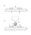
図8、9は、それぞれ本発明の保護素子の製造方法の実施形態を説明するための断面図である。 8 and 9 are cross-sectional views for describing an embodiment of a method for manufacturing a protection element of the present invention.
本実施形態に係る保護素子5の製造方法は、[1]配線31、32が形成されているとともに、被保護回路4(電子部品)が載置されている絶縁基板2を用意する工程と、[2]半導体セラミックス粒子51と未硬化の樹脂とを含む組成物50を塗布する工程と、[3]組成物50中の樹脂を硬化させることにより、保護素子5を得る工程と、を有する。以下、各工程について順次説明する。
The manufacturing method of the
[1]まず、図8(a)に示すように絶縁基板2に配線31、32を形成するとともに、被保護回路4(図8、9には図示せず。)を載置する。
[1] First, as shown in FIG. 8A, wirings 31 and 32 are formed on the insulating
配線31、32の形成方法は、特に限定されない。例えば、あらかじめ導電層を形成しパターニングする方法、導電性材料を配線パターンに沿って塗布する方法、電解または無電解めっきにより成膜する方法等が挙げられる。
The method for forming the
また、被保護回路4は、例えばリフロー処理等を経て、配線31、32と電気的に接続される。
The protected
なお、本工程は必要に応じて行えばよく、配線31、32や被保護回路4は絶縁基板2にあらかじめ配置されていてもよい。
Note that this step may be performed as necessary, and the
また、後述する保護素子5を形成した後に、被保護回路4を載置するようにしてもよい。
Further, the protected
また、絶縁基板2の表面には、必要に応じて、親液処理や撥液処理を施しておいてもよい。このうち、親液処理を施すことにより、絶縁基板2の表面と後述する組成物50との親和性が向上するため、目的とする領域に組成物50をより確実に塗布することができる。換言すれば、親液処理を施した領域では、組成物50の密着性が向上するため、組成物50から得られる保護素子5と絶縁基板2との密着性をより高めることができる。その結果、より信頼性の高い実装基板1が得られる。
Further, the surface of the insulating
一方、撥液処理が施されると、その領域では、絶縁基板2の表面と組成物50との親和性が低下し、弾かれ易くなる。これを利用することにより、組成物50を塗布する領域をより確実に制御することができる。換言すれば、組成物50を塗布すべき領域を取り囲む領域に対して撥液処理を施すことにより、目的とする領域に対して、組成物50をより簡単かつ正確に塗布することができる。
On the other hand, when the liquid-repellent treatment is performed, the affinity between the surface of the insulating
なお、親液処理や撥液処理は、組成物50の組成等に応じて適宜選択されるが、例えば、プラズマ処理、コロナ処理、電子線照射処理、カップリング剤処理、粗面化処理等が挙げられる。また、2種類以上の処理が施されてもよい。
In addition, the lyophilic treatment and the liquid repellent treatment are appropriately selected according to the composition of the
[2]
[2−1]次に、半導体セラミックス粒子51と未硬化の樹脂とを含む組成物50を調製する。
[2]
[2-1] Next, a
組成物50は、半導体セラミックス粒子51と未硬化の樹脂とを混合し、必要に応じて溶剤等で希釈されることによって液状(ペースト状)に調製される。
The
混合方法は、各成分が均一に分散混合される方法であれば、特に限定されない。具体的には、超音波分散、ディスパー、三本ロールミル、ボールミル、ビーズミル、二軸ニーダー、自公転式攪拌機等により混合される。 The mixing method is not particularly limited as long as each component is uniformly dispersed and mixed. Specifically, it is mixed by ultrasonic dispersion, a disper, a three roll mill, a ball mill, a bead mill, a twin screw kneader, a self-revolving stirrer or the like.
溶剤としては、樹脂と相溶可能なものであれば、特に限定されないが、例えば、水、ジオール類、アルコール、ポリオール、グリコールエーテル、1−メチルピロリジノン、ピリジン、ターピネオール、ブチルカルビトール、ブチルカルビトールアセテート、テキサノール、フェノキシプロパノール、エチレングリコールモノブチルエーテル、ジエチレングリコールモノブチルエーテル、エチレングリコールモノブチルエーテルアセテート、ジエチレングリコールモノブチルエーテルアセテート、γ−ブチロラクトン、エチレングリコールモノメチルエーテルアセテート、エチレングリコールモノエチルエーテルアセテート、メトキシブチルアセテート、メトキシプロピルアセテート、ジエチレングリコールモノエチルエーテルアセテート、乳酸エチル、1−オクタノール、アセトン、メチルエチルケトン、ジエチルケトン、メチルイソブチルケトン(MIBK)、トルエン、キシレン、メシチレン、酢酸エチル、シクロヘキサン、シクロヘキサノン等が挙げられ、これらのうちの1種または2種以上を含む混合溶剤であってもよい。 The solvent is not particularly limited as long as it is compatible with the resin. For example, water, diols, alcohol, polyol, glycol ether, 1-methylpyrrolidinone, pyridine, terpineol, butyl carbitol, butyl carbitol. Acetate, texanol, phenoxypropanol, ethylene glycol monobutyl ether, diethylene glycol monobutyl ether, ethylene glycol monobutyl ether acetate, diethylene glycol monobutyl ether acetate, γ-butyrolactone, ethylene glycol monomethyl ether acetate, ethylene glycol monoethyl ether acetate, methoxybutyl acetate, methoxypropyl Acetate, diethylene glycol monoethyl ether acetate, Examples include ethyl, 1-octanol, acetone, methyl ethyl ketone, diethyl ketone, methyl isobutyl ketone (MIBK), toluene, xylene, mesitylene, ethyl acetate, cyclohexane, cyclohexanone, etc., including one or more of these A mixed solvent may be used.
溶剤の使用量は、組成物50の塗布性を考慮して適宜設定されるが、一例として、半導体セラミックス粒子51と樹脂の総量に対して0.3〜50質量%程度であるのが好ましく、0.5〜30質量%程度であるのがより好ましく、1〜25質量%程度であるのがさらに好ましい。これにより、組成物50を塗布するとき、その塗布精度を高めることができ、最終的に得られる保護素子5の寸法精度を高めることができる。その結果、例えば、配線31、32が狭い領域に高密度に敷設されている場合でも、目的とする範囲に組成物50を精度よく塗布することができるようになり、高密度配線に適合した保護素子5が得られる。
The amount of the solvent used is appropriately set in consideration of the applicability of the
なお、組成物50には、前述したもの以外の添加物として、例えば分散剤、レベリング剤、粘度調整剤、消泡剤、顔料、染料のような着色剤等が添加されていてもよい。
The
着色剤としては、例えば、緑色、赤色、青色、黄色、黒色のような色を呈する染料、黒色のような色を呈する顔料、および色素からなる群から選択される1種または2種以上を含む。 Examples of the colorant include one or more selected from the group consisting of a dye exhibiting a color such as green, red, blue, yellow, and black, a pigment exhibiting a color such as black, and a pigment. .
このうち、緑色の着色剤としては、例えば、アントラキノン系、フタロシアニン系、ペリレン系のような公知の着色剤を1種または2種以上含むものが挙げられる。 Among these, examples of the green colorant include those containing one or more known colorants such as anthraquinone, phthalocyanine, and perylene.
また、黒色染料としては、例えば、アゾ系等の金属錯塩黒色染料、または、アントラキノン系化合物等の有機黒色染料などが挙げられる。当該黒色染料としては、特に限定されないが、例えば、Kayaset Black A−N(日本化薬社製)、Kayaset Black G(日本化薬社製)等が挙げられる。黒色顔料は1種または2種以上用いてもよい。 Examples of the black dye include azo-based metal complex black dyes and organic black dyes such as anthraquinone compounds. Although it does not specifically limit as the said black dye, For example, Kayase Black AN (made by Nippon Kayaku Co., Ltd.), Kayase Black G (made by Nippon Kayaku Co., Ltd.), etc. are mentioned. You may use 1 type, or 2 or more types of black pigments.
[2−2]次に、組成物50を、図8(b)に示すように、配線31と配線32との間隙33に塗布する。
[2-2] Next, the
塗布方法は、特に限定されないが、例えば、ディスペンサーやインクジェットのような吐出機を用いた方法、スキージのようなヘラを用いた方法、スクリーン印刷機のような印刷機を用いた方法等が挙げられる。このうち、図8(b)に示すように、吐出機を用いた方法が好ましく用いられる。この方法によれば、目的とする位置に必要な量の組成物50を高精度に効率よく塗布することができる。このため、組成物50の使用量を最小限に抑えつつ、短時間で塗布作業を行うことができる。その結果、塗布作業の低コスト化と高速化を図ることができる。
The application method is not particularly limited, and examples thereof include a method using a dispenser such as a dispenser or an inkjet, a method using a spatula such as a squeegee, a method using a printing machine such as a screen printing machine, and the like. . Among these, as shown in FIG. 8B, a method using a discharger is preferably used. According to this method, a necessary amount of the
その後、必要に応じて、塗布した組成物50を乾燥させる。これにより、塗布した組成物50の定着を図ることができる。
乾燥は、自然乾燥であっても、強制乾燥であってもよい。
Thereafter, the applied
Drying may be natural drying or forced drying.
なお、塗布された組成物50は、その粘度にもよるが、図9(a)に示すように、組成物50中に半導体セラミックス粒子51がほぼ均一に分散している。換言すれば、塗布前の組成物50中において半導体セラミックス粒子51が均一に分散した状態が維持されるように、組成物50の粘度が適宜設定されるのが好ましい。これにより、塗布された組成物50は、どのタイミングで塗布されたとしても、一定の濃度で半導体セラミックス粒子51が含まれたものとなる。その結果、半導体セラミックス粒子51の濃度のバラツキを抑えることができる。
Although the applied
このような粘度は、半導体セラミックス粒子51と未硬化の樹脂との間の比重差、粘度差、相溶性の他、半導体セラミックス粒子51の粒径、気温等に応じて適宜設定される。一例としては、0.1〜1000Pa・s程度であるのが好ましく、0.5〜500Pa・s程度であるのがより好ましく、1〜300Pa・s程度であるのがさらに好ましく、2〜150Pa・s程度であるのが特に好ましい。これにより、組成物50は保存安定性が良好になるとともに、塗布された組成物50の塗布精度をより高めることができる。
Such a viscosity is appropriately set according to the specific gravity difference between the
なお、粘度が前記下限値を下回ると、気温等の環境によっては、塗布された組成物50の形が崩れ易くなり、塗布精度が低下したり、塗布された組成物50において半導体セラミックス粒子51の濃度にバラツキが生じたりするおそれがある。一方、粘度が前記上限値を上回ると、気温等の環境によっては、塗布作業の作業性が低下したり、塗布精度が低下したりするおそれがある。
If the viscosity is lower than the lower limit, depending on the environment such as the temperature, the shape of the applied
上記粘度は、東機産業のTVE−33Hを使用し、25℃(室温)において測定される値である。 The viscosity is a value measured at 25 ° C. (room temperature) using Toki Sangyo TVE-33H.
[3]次に、塗布した組成物50を加熱することにより、樹脂を硬化させる。これにより、半導体セラミックス粒子51と樹脂の硬化物52とを含む保護素子5を得る。
[3] Next, the applied
組成物50の加熱条件は、組成物50の組成等に応じて適宜設定されるが、例えば50〜200℃であるのが好ましく、70〜180℃であるのがより好ましい。また、加熱時間は、例えば1〜300分であるのが好ましく、2〜120分であるのがより好ましい。これにより、配線31、32や被保護回路4の熱劣化を抑えつつ、樹脂を十分に硬化させることができる。
Although the heating conditions of the
なお、本工程は複数回に分けて行うようにしてもよい。すなわち、上述したような加熱条件で加熱した後、好ましくは50〜200℃、より好ましくは70〜180℃の加熱温度で、好ましくは0.1〜10時間、より好ましくは1〜4時間の後工程を行うようにしてもよい。 Note that this step may be performed in multiple steps. That is, after heating under the heating conditions as described above, preferably at a heating temperature of 50 to 200 ° C., more preferably 70 to 180 ° C., preferably 0.1 to 10 hours, more preferably 1 to 4 hours later. You may make it perform a process.
ここで、組成物50中の樹脂としては、本工程において加熱されたとき、初期において一旦軟化し、その後、粘度が再上昇して硬化に至るものが好ましく用いられる。軟化するタイミングでは、組成物50が配線31と配線32との間隙33により隙間なく充填されることになるため、配線31、32と保護素子5との密着性が高くなる。その結果、半導体セラミックス粒子51によるバリスタ特性の発現がより顕著になり、例えば保護素子5のエネルギー耐量といったバリスタ特性のさらなる改善が図られる。
Here, as the resin in the
一方、軟化するタイミングでは、組成物50中において半導体セラミックス粒子51が移動し易くなる。このため、半導体セラミックス粒子51と樹脂との比重差に基づき、半導体セラミックス粒子51が沈降し易くなる。このとき、図9(a)に示すように、組成物50に対して絶縁基板2が鉛直下方に位置するように配置されたときには、半導体セラミックス粒子51が絶縁基板2側に沈降する。その結果、図9(b)に示すように、配線31と配線32の間隙33にも半導体セラミックス粒子51が偏在することとなる。その結果、前述したように、間隙33に半導体セラミックス粒子51が高密度に配置されることとなり、保護素子5のバリスタ特性をより高めることができる。これにより、被保護回路4に印加される過電圧を良好に緩和することができる。
On the other hand, at the timing of softening, the
したがって、本工程においては、樹脂が軟化している最中に半導体セラミックス粒子51が沈降する必要がある。このためには、例えば、組成物50の厚さ、すなわち沈降距離と、半導体セラミックス粒子51の沈降速度とを把握することにより、軟化している時間内に沈降し終えるか否かを知ることができる。また、その結果に基づき、沈降が間に合うように、組成物50を調製すればよい。
Therefore, in this step, the
上記の観点から、半導体セラミックス粒子51の構成材料の密度は、2g/cm3以上8g/cm3以下であるのが好ましく、3g/cm3以上7g/cm3以下であるのがより好ましく、4g/cm3以上6g/cm3以下であるのがさらに好ましい。半導体セラミックス粒子51の構成材料の密度を前記範囲内に設定することにより、半導体セラミックス粒子51を十分な沈降速度で沈降させることができるので、半導体セラミックス粒子51が偏在した保護素子5をより確実に製造することができる。
From the above viewpoint, the density of the constituent material of the
なお、半導体セラミックス粒子51の構成材料の密度は、半導体セラミックス粒子51のかさ密度ではなく、その構成材料自体の密度である。
The density of the constituent material of the
また、樹脂の最小溶融(軟化)粘度は、特に限定されないが、0.001〜100Pa・sであるのが好ましく、0.01〜50Pa・sであるのがより好ましく、0.1〜30Pa・sであるのがさらに好ましい。これにより、前述したような粒子径の半導体セラミックス粒子51を用いた場合、半導体セラミックス粒子51の沈降速度が速すぎず、かつ、遅すぎない範囲に収まる。その結果、保護素子5の製造効率を高めつつ、半導体セラミックス粒子51をより確実に偏在させることができる。
The minimum melt (softening) viscosity of the resin is not particularly limited, but is preferably 0.001 to 100 Pa · s, more preferably 0.01 to 50 Pa · s, and more preferably 0.1 to 30 Pa · s. More preferably, it is s. Thereby, when the
上記粘度は、粘弾性測定装置(Rheo stress RS−10 HAAKE、サーモフィッシャーサイエンティフィック株式会社製)で昇温速度10℃/min、周波数0.1Hzで、歪み一定−応力検知で測定することができる。 The viscosity can be measured with a viscoelasticity measuring device (Rheo stress RS-10 HAAKE, manufactured by Thermo Fisher Scientific Co., Ltd.) at a heating rate of 10 ° C./min, a frequency of 0.1 Hz, and constant strain-stress detection. it can.
<電子機器>
上述したような本発明の保護素子は、種々の電子機器に搭載される。本発明の保護素子は、前述したように、空間占有率が小さくかつ配置自由度が高いものである。このため、わずかなスペースにも保護素子を配置することができ、実装基板の配線の高密度化にも親和性が高い。したがって、本発明の電子機器は、小型でかつ信頼性の高いものとなる。
<Electronic equipment>
The protection element of the present invention as described above is mounted on various electronic devices. As described above, the protection element of the present invention has a small space occupancy and a high degree of freedom in arrangement. For this reason, a protective element can be arrange | positioned in a very small space, and it has high affinity also for the densification of the wiring of a mounting substrate. Therefore, the electronic device of the present invention is small and highly reliable.
本発明の電子機器としては、例えば、携帯電話、スマートフォン、タブレット端末、ゲーム機、パソコン、テレビのような民生機器、サーバー、ルーター装置、ロボットのような産業機器の他、自動車、航空機、列車、船舶のような移動体に搭載される機器等が挙げられる。 As an electronic device of the present invention, for example, a mobile phone, a smartphone, a tablet terminal, a game machine, a personal computer, a consumer device such as a TV, a server, a router device, an industrial device such as a robot, an automobile, an aircraft, a train, Examples include equipment mounted on a moving body such as a ship.
以上、本発明について、好適な実施形態に基づいて説明したが、本発明はこれらに限定されるものではない。 As mentioned above, although this invention was demonstrated based on suitable embodiment, this invention is not limited to these.
例えば、本発明の保護素子の製造方法は、前述した実施形態に任意の工程が付加されたものであってもよく、また、前述した実施形態の工程の順序を入れ替えたものであってもよい。 For example, the manufacturing method of the protection element of the present invention may be one in which an arbitrary step is added to the above-described embodiment, or the order of the steps in the above-described embodiment may be changed. .
また、本発明の保護素子および実装基板は、前述した実施形態に任意の要素が付加されたものであってもよい。 Moreover, the protection element and the mounting substrate of the present invention may be those obtained by adding arbitrary elements to the above-described embodiment.
以下、本発明の具体的実施例について説明する。
1.実装基板の作製
(サンプルNo.1)
まず、ビスフェノールF型エポキシ樹脂とビスフェノールA型エポキシ樹脂の混合物(液状、DIC株式会社製、EPICLON EXA−830LVP)を用意した。
Hereinafter, specific examples of the present invention will be described.
1. Fabrication of mounting substrate (Sample No. 1)
First, a mixture of bisphenol F type epoxy resin and bisphenol A type epoxy resin (liquid, manufactured by DIC Corporation, EPICLON EXA-830LVP) was prepared.
また、硬化剤としてフェノールノボラック樹脂(液状、明和化成株式会社製、MEH−8000H)を用意した。 Moreover, phenol novolak resin (liquid, Meiwa Kasei Co., Ltd. make, MEH-8000H) was prepared as a hardening | curing agent.
また、シランカップリング剤として3−グリシジルオキシプロピルトリメトキシシラン(信越化学工業株式会社製、KBM−403)を用意した。 Further, 3-glycidyloxypropyltrimethoxysilane (manufactured by Shin-Etsu Chemical Co., Ltd., KBM-403) was prepared as a silane coupling agent.
また、硬化促進剤として下記式(a)で表される化合物を用意した。なお、下記式(a)のPhは、フェニル基を表す。 Moreover, the compound represented by following formula (a) was prepared as a hardening accelerator. In the following formula (a), Ph represents a phenyl group.
また、半導体セラミックス粒子(株式会社セラオン製、マイクロバリスタ、平均粒径48μm)を用意した。
なお、これらの原材料の配合比は、表1に示す通りである。
Further, semiconductor ceramic particles (manufactured by Ceraon Co., Ltd., micro varistor, average particle size 48 μm) were prepared.
The mixing ratio of these raw materials is as shown in Table 1.
次に、これらの原材料をプラネタリーミキサーで混練し、樹脂組成物を調製した。
続いて、図4に示す電気回路を含む基板として、表面に銅配線が設けられたFR−4基板を用意した。また、被保護回路として発光ダイオード素子を載置した。なお、配線の厚さは35μmであった。
Next, these raw materials were kneaded with a planetary mixer to prepare a resin composition.
Subsequently, as a substrate including the electric circuit shown in FIG. 4, an FR-4 substrate having copper wiring on the surface was prepared. In addition, a light emitting diode element was placed as a protected circuit. The wiring thickness was 35 μm.
次に、配線同士の間隙を埋めるように、調製した保護素子の形成用樹脂組成物を塗布し、スキージを用いて均した。この塗布には、ディスペンサーを使用した。 Next, the prepared resin composition for forming a protective element was applied so as to fill the gap between the wirings, and leveled using a squeegee. A dispenser was used for this application.
次いで、樹脂組成物を基準にしたときFR−4基板が鉛直下方に位置するように保持した状態で、塗布した組成物を、100℃で2分間乾燥させた後、さらに、150℃で60分間加熱し、硬化性樹脂を硬化させた。これにより、最大厚さ0.1mmの保護素子を得るとともに、実装基板を得た。 Next, the applied composition was dried at 100 ° C. for 2 minutes in a state where the FR-4 substrate was positioned vertically below when the resin composition was used as a reference, and then further at 150 ° C. for 60 minutes. The curable resin was cured by heating. As a result, a protective element having a maximum thickness of 0.1 mm was obtained and a mounting substrate was obtained.
(サンプルNo.2〜9)
原材料やその配合比を表1に示すように変更した以外は、それぞれサンプルNo.1の場合と同様にして保護素子を得るとともに、実装基板を得た。なお、一部のサンプルでは、粒径の異なる半導体セラミックス粒子を用いるようにした。
なお、表1に示す原材料は、以下の通りである。
(Sample No. 2-9)
Except for changing the raw materials and the blending ratio thereof as shown in Table 1, sample No. A protective element was obtained in the same manner as in Example 1, and a mounting substrate was obtained. In some samples, semiconductor ceramic particles having different particle diameters were used.
The raw materials shown in Table 1 are as follows.
・ビニル基含有シリコーン樹脂(液状、モメンティブ・パフォーマンス・マテリアルズ・ジャパン合同会社製、IVSM−4500(A))
・水素原子含有シリコーン樹脂(液状、モメンティブ・パフォーマンス・マテリアルズ・ジャパン合同会社製、IVSM−4500(B))
・ヒドロキシ基含有シリコーン樹脂(固形、旭化成ワッカーシリコーン株式会社製、SILRES MK)
・エポキシ系樹脂(DIC製、EPICLON EXA−830LVP)
・エポキシ系樹脂(四国化成工業製、MA−DGIC)
・硬化剤(明和化成製、MEH−8000H)
・硬化剤(新日本理化製、MH−700)
・オレフィン系樹脂(住友ベークライト製、5−デシルノルボルネン樹脂)
・ Vinyl group-containing silicone resin (liquid, Momentive Performance Materials Japan, IVSM-4500 (A))
・ Hydrogen atom-containing silicone resin (Liquid, Momentive Performance Materials Japan Ltd., IVSM-4500 (B))
・ Hydroxy group-containing silicone resin (solid, manufactured by Asahi Kasei Wacker Silicone Co., Ltd., SILRES MK)
・ Epoxy resin (DICIC, EPICLON EXA-830LVP)
・ Epoxy resin (Shikoku Kasei Kogyo, MA-DGIC)
・ Curing agent (Maywa Kasei, MEH-8000H)
・ Curing agent (manufactured by Shin Nippon Chemical Co., Ltd., MH-700)
・ Olefin resin (Sumitomo Bakelite, 5-decylnorbornene resin)
ここで、5−デシルノルボルネン樹脂は、以下に示す方法で合成した。
まず、十分に乾燥させた反応容器に酢酸エチル430g、シクロヘキサン890g、5−デシルノルボルネン223g(0.95モル)を導入した。この系中に乾燥窒素を40℃で30分間流し、溶存酸素を除去した。
Here, the 5-decylnorbornene resin was synthesized by the method shown below.
First, 430 g of ethyl acetate, 890 g of cyclohexane and 223 g of 5-decylnorbornene (0.95 mol) were introduced into a sufficiently dried reaction vessel. Dry nitrogen was passed through the system at 40 ° C. for 30 minutes to remove dissolved oxygen.
次いで、ビス(トルエン)ビス(パーフルオロフェニル)ニッケル1.33g(2.75×10⁻⁴モル)を酢酸エチル12gに溶解したものを反応系中に添加した。そして、上記の系を40℃から55℃に15分かけて昇温させた後、その温度を保持しながら3時間系中を撹拌した。 Subsequently, 1.33 g (2.75 × 10 −4 mol) of bis (toluene) bis (perfluorophenyl) nickel dissolved in 12 g of ethyl acetate was added to the reaction system. The system was heated from 40 ° C. to 55 ° C. over 15 minutes, and then the system was stirred for 3 hours while maintaining the temperature.
次いで、濃度30質量%の過酸化水素水49gを添加した純水1500gに氷酢酸26gを溶解させた溶液を調製した。そして、上記の系に調製した溶液を加え、50℃で5時間撹拌した後、撹拌を止め、分離した水層を除去した。 Next, a solution was prepared by dissolving 26 g of glacial acetic acid in 1500 g of pure water to which 49 g of hydrogen peroxide having a concentration of 30% by mass was added. And the solution prepared to said system was added, and after stirring at 50 degreeC for 5 hours, stirring was stopped and the isolate | separated water layer was removed.
次いで、水層の除去によって残った有機層を、メタノール220gとイソプロピルアルコール200gとを用いて洗浄した。 Next, the organic layer remaining after the removal of the aqueous layer was washed with 220 g of methanol and 200 g of isopropyl alcohol.
次いで、洗浄後の有機層に、シクロヘキサン510gと酢酸エチル290gとを添加し、系を均一に溶解した。 Next, 510 g of cyclohexane and 290 g of ethyl acetate were added to the washed organic layer to uniformly dissolve the system.
次いで、得られた溶液に、メタノール156gおよびイソプロピルアルコール167gからなる溶媒を添加した後、撹拌し、さらに添加した溶媒を除去する処理を行った。この処理を2回繰り返すことにより、有機層の洗浄を行った。 Next, a solvent consisting of 156 g of methanol and 167 g of isopropyl alcohol was added to the obtained solution, followed by stirring, and a process for removing the added solvent. The organic layer was washed by repeating this treatment twice.
次いで、洗浄後の有機層にシクロヘキサン180mlを添加して系を均一に溶解し、さらにメシチレン670gを添加した。そして、減圧下にてロータリーエバポレーターでシクロヘキサンを蒸発除去することにより、5−デシルノルボルネン重合体543g(35%のメシチレン溶液)を得た。 Next, 180 ml of cyclohexane was added to the washed organic layer to uniformly dissolve the system, and 670 g of mesitylene was further added. Then, 543 g (35% mesitylene solution) of 5-decylnorbornene polymer was obtained by evaporating and removing cyclohexane with a rotary evaporator under reduced pressure.
合成した5−デシルノルボルネン重合体について、ゲル浸透クロマトグラフィー(GPC)により重量平均分子量を測定したところ、75,300であった。 The synthesized 5-decylnorbornene polymer was measured to have a weight average molecular weight of 75,300 by gel permeation chromatography (GPC).
なお、常温下で固形の原材料については、常温下で液状の原材料と混合し、その後、固形の原材料を加熱溶融した後に、塗布作業に用いるようにした。 In addition, about the raw material solid at normal temperature, it mixed with the liquid raw material at normal temperature, and it was made to use for an application | coating operation | work after heat-melting solid raw material after that.
(サンプルNo.10)
まず、樹脂組成物として、原材料やその配合比を表1に示すように変更したものを用意した。
(Sample No. 10)
First, as the resin composition, a raw material and a mixture ratio thereof changed as shown in Table 1 were prepared.
次いで、サンプルNo.1の実装基板を製造する方法と同様にして、樹脂組成物を塗布し、スキージを用いて均した後、天地を反転させた。そして、樹脂組成物を基準にしたときにFR−4基板が鉛直上方に位置するように保持した状態で、塗布した組成物を乾燥、硬化させた。これにより、保護素子を得るとともに実装基板を得た。
なお、表1に示す原材料は、以下の通りである。
Next, sample no. The resin composition was applied in the same manner as in the method of manufacturing the mounting substrate 1 and leveled using a squeegee, and then the top and bottom were inverted. Then, the applied composition was dried and cured in a state where the FR-4 substrate was held vertically above when the resin composition was used as a reference. Thereby, a protective element was obtained and a mounting substrate was obtained.
The raw materials shown in Table 1 are as follows.
・ビニル基含有シリコーン樹脂(液状、信越化学工業株式会社製、KE−106)
・水素原子含有シリコーン樹脂(液状、信越化学工業株式会社製、CAT−RG)
・ Vinyl group-containing silicone resin (liquid, manufactured by Shin-Etsu Chemical Co., Ltd., KE-106)
・ Hydrogen atom-containing silicone resin (liquid, manufactured by Shin-Etsu Chemical Co., Ltd., CAT-RG)
(サンプルNo.11)
原材料やその配合比を表1に示すように変更した以外は、サンプルNo.10の場合と同様にして保護素子を得るとともに、実装基板を得た。
(Sample No. 11)
Except for changing the raw materials and the blending ratio thereof as shown in Table 1, sample No. A protective element was obtained in the same manner as in No. 10, and a mounting substrate was obtained.
(サンプルNo.12)
ディスペンサーを用いて樹脂組成物を塗布した後、スキージを用いた均し作業を省略するようにした以外は、サンプルNo.1の場合と同様にして保護素子を得るとともに、実装基板を得た。
なお、使用した原材料やその配合比を表2に示す。
(Sample No. 12)
After applying the resin composition using the dispenser and then omitting the leveling operation using the squeegee, the sample No. A protective element was obtained in the same manner as in Example 1, and a mounting substrate was obtained.
In addition, Table 2 shows the raw materials used and their blending ratios.
また、保護素子の上面を光学顕微鏡で観察したところ、湾曲凸面を呈していることが認められた。 Moreover, when the upper surface of the protective element was observed with an optical microscope, it was recognized that it had a curved convex surface.
(サンプルNo.13)
まず、サンプルNo.1の場合と同様にして、樹脂組成物を調製した。なお、樹脂組成物の原材料やその配合比は表2に示す通りである。
(Sample No. 13)
First, sample no. In the same manner as in the case of 1, a resin composition was prepared. The raw materials of the resin composition and the blending ratio are as shown in Table 2.
次いで、図7に示す電気回路を含む基板として、表面に銅配線およびソルダーレジスト膜が設けられたFR−4基板を用意した。なお、隣り合う銅配線とその配線間とが露出するように、ソルダーレジスト膜には開口を設けるようにした。また、被保護回路として発光ダイオード素子を載置した。なお、配線の厚さは35μmであった。 Next, as a substrate including the electric circuit shown in FIG. 7, an FR-4 substrate having a copper wiring and a solder resist film provided on the surface was prepared. Note that an opening was provided in the solder resist film so that the adjacent copper wiring and the space between the wirings were exposed. In addition, a light emitting diode element was placed as a protected circuit. The wiring thickness was 35 μm.
次に、ソルダーレジスト膜の開口を埋めるように、調製した樹脂組成物を塗布した。この塗布には、ディスペンサーを使用した。 Next, the prepared resin composition was applied so as to fill the opening of the solder resist film. A dispenser was used for this application.
次いで、サンプルNo.1の場合と同様にして、樹脂組成物を硬化させ、最大厚さ0.1mmの保護素子を得るとともに、実装基板を得た。 Next, sample no. In the same manner as in case 1, the resin composition was cured to obtain a protective element having a maximum thickness of 0.1 mm and a mounting substrate.
なお、ソルダーレジスト膜の厚さは30μm、保護素子とソルダーレジスト膜とが重なっている部分の長さL1は60〜1500μmであった。 The thickness of the solder resist film was 30 μm, and the length L1 of the portion where the protective element and the solder resist film overlapped was 60 to 1500 μm.
(サンプルNo.14)
長さL1が30〜2000μmである以外は、サンプルNo.13と同様にして保護素子を得るとともに、実装基板を得た。
(Sample No. 14)
Sample No. 1 except that the length L1 is 30 to 2000 μm. In the same manner as in Example 13, a protective element was obtained and a mounting substrate was obtained.
(サンプルNo.15)
長さL1が15〜3000μmである以外は、サンプルNo.13と同様にして保護素子を得るとともに、実装基板を得た。
(Sample No. 15)
Sample No. 1 except that the length L1 is 15 to 3000 μm. In the same manner as in Example 13, a protective element was obtained and a mounting substrate was obtained.
(サンプルNo.16)
長さL1が0〜3000μmである以外は、サンプルNo.13と同様にして保護素子を得るとともに、実装基板を得た。
(Sample No. 16)
Sample No. except that the length L1 is 0 to 3000 μm. In the same manner as in Example 13, a protective element was obtained and a mounting substrate was obtained.
2.樹脂組成物の評価
サンプルNo.1〜11における実装基板の製造に際して使用した樹脂組成物について、それぞれ、室温での粘度、および150℃まで加熱したときの最低溶融粘度と150℃での粘度とを測定した。なお、粘度の測定は、粘弾性測定装置(Rheo stress RS−10 HAAKE、サーモフィッシャーサイエンティフィック株式会社製)を用い、昇温速度10℃/min、周波数0.1Hzの条件下で、歪み一定−応力検知による測定方法にて実施した。測定結果を表1に示す。
2. Evaluation of Resin Composition Sample No. About the resin composition used in the case of manufacture of the mounting board | substrate in 1-11, the viscosity at room temperature and the minimum melt viscosity when heated to 150 degreeC and the viscosity in 150 degreeC were measured, respectively. The viscosity was measured using a viscoelasticity measuring apparatus (Rheo stress RS-10 HAAKE, manufactured by Thermo Fisher Scientific Co., Ltd.) under the conditions of a heating rate of 10 ° C./min and a frequency of 0.1 Hz. -It carried out by the measuring method by stress detection. The measurement results are shown in Table 1.
3.実装基板の評価
3.1 沈降度合いの評価
各サンプルNo.においてそれぞれ複数個の実装基板を製造し、そのうちの1つについて、保護素子の断面を観察するために切断した。そして、切断面を走査型電子顕微鏡で観察したところ、半導体セラミックス粒子がFR−4基板側に偏在していることが認められた。そこで、切断面の観察像から、保護素子の中間線を求め、その中間線よりもFR−4基板側における半導体セラミックス粒子の面積率(体積率)を1としたとき、中間線よりもFR−4基板から遠い側(反対側)における半導体セラミックス粒子の面積率(体積率)の相対値を算出した。算出結果を表1、2に示す。
3. Evaluation of mounted substrate 3.1 Evaluation of sedimentation degree A plurality of mounting substrates were manufactured, and one of them was cut to observe the cross section of the protective element. When the cut surface was observed with a scanning electron microscope, it was found that the semiconductor ceramic particles were unevenly distributed on the FR-4 substrate side. Therefore, an intermediate line of the protective element is obtained from the observation image of the cut surface, and when the area ratio (volume ratio) of the semiconductor ceramic particles on the FR-4 substrate side from the intermediate line is 1, FR- The relative value of the area ratio (volume ratio) of the semiconductor ceramic particles on the side far from the four substrates (opposite side) was calculated. The calculation results are shown in Tables 1 and 2.
なお、算出にあたっては、観察像に二値化の画像処理を施し、セラミックス粒子の輪郭が明瞭になるようにした。 In the calculation, binarized image processing was performed on the observed image so that the outline of the ceramic particles became clear.
3.2 電気特性(初期のバリスタ特性)の評価
pA meter/DC VOLTAGE SOURCE 4140B(アジレントテクノロジー株式会社製)を用いて、実装基板において隣り合う配線間に0Vから100Vまで昇圧速度0.5V/secで印加した時に流れた電流値を測定した。このようにして得られた電流・電圧特性の結果に基づいて、図10に示すように、対数軸でプロットしたグラフを作成した。次いで、得られたグラフから、非直線係数を算出した。そして、各サンプルNo.の樹脂組成物の硬化物が示すバリスタ特性については、算出した非直線係数の値から以下の基準で評価を行った。
3.2 Evaluation of electrical characteristics (initial varistor characteristics) Using a pA meter / DC VOLTAGSOURCE SOURCE 4140B (manufactured by Agilent Technologies), a boosting speed of 0.5 V / sec from 0 V to 100 V between adjacent wirings on the mounting board The value of the current that flowed when the voltage was applied was measured. Based on the results of the current / voltage characteristics thus obtained, a graph plotted with a logarithmic axis was created as shown in FIG. Next, a non-linear coefficient was calculated from the obtained graph. And each sample No. About the varistor characteristic which the hardened | cured material of this resin composition shows, it evaluated on the following references | standards from the value of the calculated nonlinear coefficient.
◎:非直線係数が20以上である。
○:非直線係数が10以上20未満である。
△:非直線係数が2以上10未満である。
×:非直線係数が2未満であり、バリスタ電圧が発現しなかった。
評価結果を表1、2に示す。
A: The nonlinear coefficient is 20 or more.
A: The nonlinear coefficient is 10 or more and less than 20.
Δ: The nonlinear coefficient is 2 or more and less than 10.
X: The non-linear coefficient was less than 2, and no varistor voltage was developed.
The evaluation results are shown in Tables 1 and 2.
3.3 耐候性(耐塩水噴霧試験)の評価
まず、サンプルNo.13〜16の実装基板を、塩水噴霧試験装置に投入した。そして、0.5質量%の塩化ナトリウムと、0.2%の過酸化水素と、を含む水溶液を塩溶液として調製し、これを実装基板に対して96時間噴霧した。なお、噴霧室内の温度は35℃とした。
3.3 Evaluation of weather resistance (salt water spray test) First, sample no. 13 to 16 mounting boards were put into a salt spray test apparatus. And the aqueous solution containing 0.5 mass% sodium chloride and 0.2% hydrogen peroxide was prepared as a salt solution, and this was sprayed with respect to the mounting substrate for 96 hours. The temperature in the spray chamber was 35 ° C.
次いで、24時間経過後の実装基板20個、および、96時間経過後の実装基板20個をそれぞれ切断し、保護素子近傍の銅配線における発錆の有無を光学顕微鏡によって観察した。そして、観察結果を以下の評価基準に照らして評価した。 Next, 20 mounting substrates after 24 hours and 20 mounting substrates after 96 hours were cut, respectively, and the presence or absence of rusting in the copper wiring near the protective element was observed with an optical microscope. And the observation result was evaluated in light of the following evaluation criteria.
<発錆の評価基準>
◎:発錆数が0個である
○:発錆数が1または2個である
△:発錆数が3〜5個である
×:発錆数が6個以上である
評価結果を表2に示す。
<Evaluation criteria for rusting>
A: The number of rusting is 0. B: The number of rusting is 1 or 2. B: The number of rusting is 3-5. X: The number of rusting is 6 or more. Shown in
3.4 ESD耐性の評価
まず、実装基板の隣接した回路間に5回の放電を行った。なお、放電条件は、放電容量が100pF、放電抵抗が1500Ωであった。また、放電試験には、静電気試験器(株式会社ノイズ研究所製、ESS−6008)を使用した。
3.4 Evaluation of ESD resistance First, five discharges were performed between adjacent circuits on the mounting substrate. The discharge conditions were a discharge capacity of 100 pF and a discharge resistance of 1500Ω. Moreover, the static electricity tester (Noise Research Institute make, ESS-6008) was used for the discharge test.
次いで、pA meter/DC VOLTAGE SOURCE 4140B(アジレントテクノロジー社製)を用いて隣接した回路間に0Vから100Vまで昇圧速度0.5V/秒で電圧を印加した。そして、5Vの電圧が印加されたときに回路間に流れた電流値を測定し、得られた測定値を以下の評価基準に照らして評価した。 Next, a voltage was applied from 0 V to 100 V at a boosting rate of 0.5 V / second between adjacent circuits using pA meter / DC VOLTAG SOURCE 4140B (manufactured by Agilent Technologies). Then, the current value flowing between the circuits when a voltage of 5 V was applied was measured, and the obtained measured value was evaluated in light of the following evaluation criteria.
<ESD耐性の評価基準>
○:電流値が1.0×10⁻⁶A未満である
△:電流値が1.0×10⁻⁶A以上1.0×10⁻³A未満である
×:電流値が1.0×10⁻³A以上である
以上の評価結果を表1、2に示す。
<Evaluation criteria for ESD resistance>
○: Current value is less than 1.0 × 10 −6 A Δ: Current value is 1.0 × 10 −6 A or more and less than 1.0 × 10 −3 A ×: Current value is 1.0 × 10 −3 A or more The above evaluation results are shown in Tables 1 and 2.
表1、2から明らかなように、各実施例の実装基板では、いずれも、保護素子におけるバリスタ特性を確認することができた。さらに、断面の観察等の結果から保護素子の密着性も良好であった。これらのことから、本発明によれば、目的とする位置に高い配置自由度で保護素子を容易に製造し得ることが明らかとなった。 As is clear from Tables 1 and 2, the varistor characteristics of the protective element could be confirmed in any of the mounting substrates of the examples. Furthermore, the adhesion of the protective element was also good from the results of cross-sectional observation and the like. From these facts, it became clear that according to the present invention, the protective element can be easily manufactured at a target position with a high degree of freedom in arrangement.
さらに、保護素子をソルダーレジスト膜と重なるように配置することで、実装基板の耐候性を高め得ることも認められた。 Furthermore, it was recognized that the weather resistance of the mounting substrate can be improved by arranging the protective element so as to overlap the solder resist film.
1 実装基板
2 絶縁基板
4 被保護回路
5 保護素子
6 電源
7 ソルダーレジスト膜
13F 試験片
31 配線
32 配線
33 間隙
41 対電極
42 主電極
43 ガード電極
50 組成物
51 半導体セラミックス粒子
52 硬化物
71 開口
311 幹線
312 支線
315 分岐点
321 幹線
322 支線
325 分岐点
511 粒界部
512 結晶部
Z0 ラインインピーダンス
DESCRIPTION OF SYMBOLS 1
Claims (11)
粒界部と前記粒界部によって離隔される複数の結晶部とを含む半導体セラミックス粒子と、比誘電率4以下の樹脂の硬化物と、を有し、
前記半導体セラミックス粒子が前記基部側に偏在していることを特徴とする保護素子。 A protection element that is provided across the conductive parts that are spaced apart from each other on the surface of the base part, and exhibits non-linearity in which the voltage-current characteristic does not follow Ohm's law,
A semiconductor ceramic particle including a grain boundary part and a plurality of crystal parts separated by the grain boundary part, and a cured product of a resin having a relative dielectric constant of 4 or less,
A protective element, wherein the semiconductor ceramic particles are unevenly distributed on the base side.
粒界部と前記粒界部によって離隔される複数の結晶部とを含む半導体セラミックス粒子と、硬化性の樹脂の硬化物と、を有し、
前記半導体セラミックス粒子が前記基部側に偏在していることを特徴とする保護素子。 A protection element that is provided across the conductive parts that are spaced apart from each other on the surface of the base part, and exhibits non-linearity in which the voltage-current characteristic does not follow Ohm's law,
Semiconductor ceramic particles including a grain boundary part and a plurality of crystal parts separated by the grain boundary part, and a cured product of a curable resin,
A protective element, wherein the semiconductor ceramic particles are unevenly distributed on the base side.
前記組成物中の前記硬化性樹脂を硬化させることにより、電圧−電流特性がオームの法則に従わない非直線性を示す保護素子を形成する工程と、
を有することを特徴とする保護素子の製造方法。 Applying a composition comprising semiconductor ceramic particles including a grain boundary part and a plurality of crystal parts separated by the grain boundary part, and an uncured curable resin;
Curing the curable resin in the composition to form a protective element exhibiting non-linearity in which voltage-current characteristics do not follow Ohm's law;
The manufacturing method of the protection element characterized by having.
前記組成物を塗布する工程において、前記導電部同士を跨ぐ領域に前記組成物を塗布する請求項6に記載の保護素子の製造方法。 Provided before the step of applying the composition, a base, a plurality of conductive parts provided on the surface of the base and spaced apart from each other, and an electronic component electrically connected to the conductive part are arranged Further comprising the step of preparing an insulating member,
The method for manufacturing a protection element according to claim 6, wherein in the step of applying the composition, the composition is applied to a region straddling the conductive portions.
前記基部の表面上に設けられ、互いに離間する複数の導電部と、
前記導電部と電気的に接続されている電子部品と、
前記導電部同士を跨いで設けられ、粒界部と前記粒界部によって離隔される複数の結晶部とを含む半導体セラミックス粒子と、硬化性樹脂の硬化物と、を含み、電圧−電流特性がオームの法則に従わない非直線性を示す保護素子と、
を有し、
前記保護素子において前記半導体セラミックス粒子が前記基部側に偏在していることを特徴とする実装基板。 The base,
A plurality of conductive portions provided on the surface of the base and spaced apart from each other;
An electronic component electrically connected to the conductive portion;
The semiconductor ceramic particles, which are provided across the conductive parts and include a grain boundary part and a plurality of crystal parts separated by the grain boundary part, and a cured product of a curable resin, have a voltage-current characteristic. A protective element exhibiting non-linearity that does not follow Ohm's law;
Have
In the protective element, the semiconductor ceramic particles are unevenly distributed on the base side.
前記保護素子は、前記開口から前記ソルダーレジスト膜の表面上にはみ出すように設けられている請求項9に記載の実装基板。 Furthermore, a solder resist film is provided so as to cover a part on the surface of the conductive portion, and has an opening corresponding to a region including a gap between the conductive portions,
The mounting substrate according to claim 9, wherein the protective element is provided so as to protrude from the opening onto the surface of the solder resist film.
Applications Claiming Priority (4)
| Application Number | Priority Date | Filing Date | Title |
|---|---|---|---|
| JP2015228076 | 2015-11-20 | ||
| JP2015228076 | 2015-11-20 | ||
| JP2015251984 | 2015-12-24 | ||
| JP2015251984 | 2015-12-24 |
Publications (1)
| Publication Number | Publication Date |
|---|---|
| JP2017120879A true JP2017120879A (en) | 2017-07-06 |
Family
ID=59272524
Family Applications (1)
| Application Number | Title | Priority Date | Filing Date |
|---|---|---|---|
| JP2016176807A Pending JP2017120879A (en) | 2015-11-20 | 2016-09-09 | Protection element, manufacturing method of protection element, mounting substrate, and electronic device |
Country Status (1)
| Country | Link |
|---|---|
| JP (1) | JP2017120879A (en) |
Cited By (1)
| Publication number | Priority date | Publication date | Assignee | Title |
|---|---|---|---|---|
| CN110072326A (en) * | 2018-01-20 | 2019-07-30 | 庆鼎精密电子(淮安)有限公司 | Multilayer circuit board and its manufacturing method |
-
2016
- 2016-09-09 JP JP2016176807A patent/JP2017120879A/en active Pending
Cited By (2)
| Publication number | Priority date | Publication date | Assignee | Title |
|---|---|---|---|---|
| CN110072326A (en) * | 2018-01-20 | 2019-07-30 | 庆鼎精密电子(淮安)有限公司 | Multilayer circuit board and its manufacturing method |
| CN110072326B (en) * | 2018-01-20 | 2020-07-24 | 庆鼎精密电子(淮安)有限公司 | Multilayer circuit board and method for manufacturing same |
Similar Documents
| Publication | Publication Date | Title |
|---|---|---|
| CN101356643B (en) | Semiconductor device | |
| KR102131628B1 (en) | Adhesive composition and adhesive sheet, and hardened article and semiconductor device using same | |
| KR102900411B1 (en) | Resin compositions | |
| TWI882013B (en) | Thermosetting resin composition, thermosetting resin sheet, electronic component, and electronic device | |
| KR20130141530A (en) | Adhesive composition, adhesive sheet, and semiconductor device using the adhesive composition or the adhesive sheet | |
| JPWO2011089922A1 (en) | Polyimide resin composition, adhesive containing the same, laminate and device | |
| TW201730270A (en) | Epoxy resin composition, method for producing the same, and use of the composition | |
| US10717806B2 (en) | Packaging material and film | |
| TWI453253B (en) | Resin composition | |
| TW201809050A (en) | Curable composition, cured film using said composition and overcoat film | |
| JP7287348B2 (en) | resin composition | |
| KR102186795B1 (en) | Adhesive composition and adhesive film having same, substrate provided with adhesive composition, and semiconductor device and method for manufacturing same | |
| JP2009224109A (en) | Insulation sheet and laminated structural body | |
| CN114479349A (en) | Resin composition | |
| KR20210113069A (en) | Method for manufacturing semiconductor device, and resin sheet | |
| KR20220103974A (en) | Varistor-forming paste, cured product thereof, and varistor | |
| JP2017120879A (en) | Protection element, manufacturing method of protection element, mounting substrate, and electronic device | |
| US20240371823A1 (en) | Method for producing circuit board and resin sheet used therein | |
| TW202505713A (en) | Multi-chip module substrate | |
| JP7604873B2 (en) | Thermosetting resin composition and semiconductor device | |
| WO2023228815A1 (en) | Resin composition, cured product, antenna element and electronic component | |
| JP7180324B2 (en) | Resin composition, adhesive sheet and multilayer substrate | |
| KR20190103870A (en) | Epoxy resin composition for molding semiconductor, molding film and semiconductor package using the same | |
| KR20220056134A (en) | Resin composition for use in sealing | |
| KR102091763B1 (en) | Resin composite and led package comprising insulationlayer comprising the same |